ICGOO在线商城 > UNR5218G0L
 Datasheet下载
- 型号: UNR5218G0L
- 制造商: Panasonic Corporation
- 库位|库存: xxxx|xxxx
- 要求:
| 数量阶梯 | 香港交货 | 国内含税 |
| +xxxx | $xxxx | ¥xxxx |
查看当月历史价格
查看今年历史价格
UNR5218G0L产品简介:
ICGOO电子元器件商城为您提供UNR5218G0L由Panasonic Corporation设计生产,在icgoo商城现货销售,并且可以通过原厂、代理商等渠道进行代购。 提供UNR5218G0L价格参考以及Panasonic CorporationUNR5218G0L封装/规格参数等产品信息。 你可以下载UNR5218G0L参考资料、Datasheet数据手册功能说明书, 资料中有UNR5218G0L详细功能的应用电路图电压和使用方法及教程。
| 参数 | 数值 |
| 产品目录 | |
| 描述 | TRANS PREBIAS NPN 150MW SMINI3 |
| 产品分类 | 晶体管(BJT) - 单路﹐预偏压式 |
| 品牌 | Panasonic Electronic Components |
| 数据手册 | http://industrial.panasonic.com/www-cgi/jvcr13pz.cgi?E+SC+4+BFA7001+UNR5218G+8+WW |
| 产品图片 |
|
| 产品型号 | UNR5218G0L |
| rohs | 无铅 / 符合限制有害物质指令(RoHS)规范要求 |
| 产品系列 | - |
| 不同 Ib、Ic时的 Vce饱和值(最大值) | 250mV @ 300µA, 10mA |
| 不同 Ic、Vce 时的DC电流增益(hFE)(最小值) | 20 @ 5mA,10V |
| 产品目录绘图 |
|
| 产品目录页面 | |
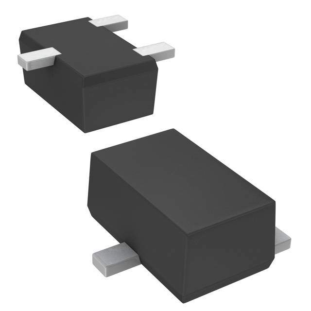
| 供应商器件封装 | S迷你型3-F2 |
| 其它名称 | UNR5218G0LTR |
| 功率-最大值 | 150mW |
| 包装 | 带卷 (TR) |
| 安装类型 | 表面贴装 |
| 封装/外壳 | SC-85 |
| 晶体管类型 | NPN - 预偏压 |
| 标准包装 | 3,000 |
| 电压-集射极击穿(最大值) | 50V |
| 电流-集电极(Ic)(最大值) | 100mA |
| 电流-集电极截止(最大值) | 500nA |
| 电阻器-发射极基底(R2)(Ω) | 5.1k |
| 电阻器-基底(R1)(Ω) | 510 |
| 频率-跃迁 | 150MHz |


- 商务部:美国ITC正式对集成电路等产品启动337调查
- 曝三星4nm工艺存在良率问题 高通将骁龙8 Gen1或转产台积电
- 太阳诱电将投资9.5亿元在常州建新厂生产MLCC 预计2023年完工
- 英特尔发布欧洲新工厂建设计划 深化IDM 2.0 战略
- 台积电先进制程称霸业界 有大客户加持明年业绩稳了
- 达到5530亿美元!SIA预计今年全球半导体销售额将创下新高
- 英特尔拟将自动驾驶子公司Mobileye上市 估值或超500亿美元
- 三星加码芯片和SET,合并消费电子和移动部门,撤换高东真等 CEO
- 三星电子宣布重大人事变动 还合并消费电子和移动部门
- 海关总署:前11个月进口集成电路产品价值2.52万亿元 增长14.8%


PDF Datasheet 数据手册内容提取
This product complies with the RoHS Directive (EU 2002/95/EC). Transistors with built-in Resistor UNR521xG Series Silicon NPN epitaxial planar type For digital circuits / e ■ Features ■ Package •Costs can be reduced through downsizing of the equipmenct and •Code reduction of the number of parts SMini3d-F2 •S-Mini type package, allowing automatic insertion thronugh the tape •Pin Name packing and magazine packing e1: Base e. a 2: Emitter g a ■ Resistance by Part Number u3: Collector st •UNR5210G Markin8gL symboln4(7R k1Ω) (R2) ■ Internal Connyeclcet ion n c ••UUNNRR55221112GG 88ABe1202 kkΩΩ 1202 kkΩΩ ct lifRe1 C •UNR5213G 8C 47 kΩ 47i kΩ duB ••UUNNRR55221154GG nt88ED 1100 kkΩΩnt47 kΩ r Pro R2 E u •UNR5216G 8F 4.7 kΩ o •UNR5217Gi 8H o22 kΩ g f pe n. n y o •••••••••••UUUUUUUUUUUMNNNNNNNNNNNRRRRRRRRRRR555555555552222222222211111111111aVTNLMKDEF98GGGGGGGGGGGDisEEE8888F888OQKNIPMDLZXcDisco024442n2414.t1.....5i270727772 1 kn kkkk kkkkkΩkuΩΩΩΩΩΩΩΩΩΩed ipnl24454441112cal....77700022771nu kkkkkkkkkkkedΩΩΩΩΩΩΩΩΩΩΩde pls mamfanaoiillenntotd eewdindiniasasncnccocoenen t ttitgi ynnpuUueeeRddL ttoayynb.ppopeeuadt nlaatseosnti ic.ncfoo.rjpm/aetin/ •UNR521ZG cFe/F 4.7 kΩ 22 kΩ win mic n o e ■ Absolute Maxinmteunma Ratings Ta = 25°C sit follww.s Paramaieter Symbol Rating vUinit w Collector-base voMltage (Emitter open) V 50 se V p:// CBO ea htt Collector-emitter voltage (Base open) VCEO 5P0l V Collector current I 100 mA C Total power dissipation P 150 mW T Junction temperature T 150 °C j Storage temperature T −55 to +150 °C stg Publication date: June 2007 SJH00218AED 1
This product complies with the RoHS Directive (EU 2002/95/EC). UNR521xG Series ■ Electrical Characteristics T = 25°C ± 3°C a Parameter Symbol Conditions Min Typ Max Unit Collector-base voltage (Emitter open) V I = 10 µA, I = 0 50 V CBO C E Collector-emitter voltage (Base open) V I = 2 mA, I = 0 50 V CEO C B Collector-base cutoff current (Emitter open) I V = 50 V, I = 0 0.1 µA CBO CB E / Collector-emitter cutoff current (Base open) ICEO VCE = 50 V, IB = 0 e 0.5 Emitter-base UNR5210G/5215G/5216G/5217G I V = 6 V, I = 0 0.01 mA EBO EB C cutoff current UNR5213G c 0.1 (Collector UNR5212G/5214G/521DG/ d 0.2 open) 521EG/521MG/521NG/521TG n UNR521ZG e 0.4e. a g UNR5211G a0.5 UNR521FG/521KG u e st1.0 UNR5219G n cl 1.5 y n c UNR5218G/521LG/521VG e 2.0 Forward UNR521VG ehFE VCE = 10 V, IC = 5 mA ct l6if 20 i u current UNR5218G/521KG/521LG d 20 t t o trraatniosfer UUNNRR55221191GnG/521DG/521FG n ur Pr 3305 o UNiR5212G/521EG o g f pe 60 n. COOoMuulttlppeuucttt ovvroo-elalttmUUUUUUUUaaNggiNNNNNNNtReetR5 RRRR ReR2lhD5ro1555555 i02wsg2G222221ah*i111111-3/t5-luVDZEN3G2elr1eGGGv/GGGa55vGet/2e/i5l*5o1/l5242n2s11G1 6vKGT/o5*GG/cl25t21ae1Mg/7GceG*DiscVoVVCnEtOOi(HLsant)ued iIVVIVVVpCCnlCCCC c==aCCCCl 11n=====u00 ed55555 mm deVVVVV pAAls,,,,, m,,amVVVVVf IIanaoBBBBBBiil le=======nnto t d1023601 ee0......w555035din din V iVVVVmmnasas, ,,,,AAnc RncRRRRwcoLcioLLL e =nenn==== t t tit 1gi1111 y nyn kkkkkpuΩUuΩΩΩΩeemeRiddLc ttoayynb.pp1op4e688e6.000uad90t nlaatseosnti ic.ncfo0o2440.r.j060.22000p5m/aetin/oVVV n CC B o L e TInrpauntsition fUreNquRe5n2c1y8ntGena RfT1 VCB = 10 V, IEs i=t f−2ol lmA,w f w=. 2s00 MHz −30% 01.5501 +30% MkHΩz ai vi w resistance UNRM5219G se p:// 1.0 UNR521MG/521VG ea htt 2.2 UNR5216G/521FG/521LG/ Pl 4.7 521NG/521ZG UNR5211G/5214G/5215G/521KG 10 UNR5212G/5217G/521TG 22 UNR5210G/5213G/521DG/521EG 47 Note)1.Measuring methods are based on JAPANESE INDUSTRIAL STANDARD JIS C 7030 measuring methods for transistors. 2.*:Rank classification Rank Q R S No-rank h 160 to 260 210 to 340 290 to 460 160 to 460 FE 2 SJH00218AED
This product complies with the RoHS Directive (EU 2002/95/EC). UNR521xG Series ■ Electrical Characteristics (continued) T = 25°C ± 3°C a Parameter Symbol Conditions Min Typ Max Unit Resistance UNR521MG R/R 0.047 1 2 ratio UNR521NG 0.1 UNR5218G/5219G 0.08 0.10 0.12 / UNR521ZG 0.21 e UNR5214G 0.17 0.21 0.25 UNR521TG 0.47 c UNR521FG d0.37 0.47 0.57 UNR521VG n 1.0 UNR5211G/5212G/5213G/521LG e 0.8 1.0 1.2 e. UNR521KG a 1.70 2.13 2g.60 a UNR521EG u 1.70 2.14 st2.60 UNR521DG n 3.7 c4l.7e 5.7 y Note)Measuring methods are based on JAPANESE INDUSTRIAL nSTANDARD JIS C 7030 measurincg methods for transistors. e Common characteristics chaert ct lif i u PT Tat t od r 240 n n r P u o ()Total power dissipation P mWTM211062840000000 Amabi4ei0nt Dtemip8e0rature s T12a0 (°C)cD1i6s0coontinued ipnlcalnuedde pls mamfanaoiillenntotd eewdindininasasgncnc fcocoenen t ttitgi ynynpuUpueeeeRddL ttoayynb.ppopeeuadt nlaatseosnti ic.ncfoo.rjpm/aetin/on. Characteristics charts of cUeN/R5210G win mic n o e ()Collector current I mAC 6543200000 IB = 01I..M300C .m m9ai 0AmA.8nA tm0V.A7e C0mnE.6A0a .m5T0 aAm. 4=A 0m2.51A° mCA ()mitter saturation voltage V VCE(sat)11010−1012 PleVasCEe2( 5s°avCti) hsittt fpIT:Co/aI l/C=l /7 wI5B° =Cw 10w.s ward current transfer ratio hFE123400000000 hFE TIaC = −2V7525C°5°EC°C =C 10 V 10 or-e For ect −25°C oll 0 C 10−2 0 0 2 4 6 8 10 12 10−1 1 10 102 1 10 102 103 Collector-emitter voltage VCE (V) Collector current IC (mA) Collector current IC (mA) SJH00218AED 3
This product complies with the RoHS Directive (EU 2002/95/EC). UNR521xG Series C V I V V I ob CB O IN IN O (pF)Cob 65 fIT E=a = =1 0 2M5°HCz 104 VTaO = = 2 55 °VC 102 VTaO = = 2 05.°2C V or output capacitancemon base, input open circuited) 4321 µ()Output current I AO 11100023 nce/(V)Input voltage V IN1d01 −101 Collect (Com 100 −1Collector-1base voltag1e0 VCB (V)102 10.a4 0I.6nput v0o.8ltage 1 V.0IN (Vu1).2 1.4e10 −120 −1 Outpu1t ec ursrtenat g IOe1 .0 (mA) 102 n cl y n c e Characteristics charts of UNeR5211G ct lif I V iV I u h I C CE CE(sat) C d FE C t t o ()Collector current I mACM114286000000Collea2ct0o.i08rI-. B9me =4DmmA 1Ai.t0tie mr6 Anvoltag8se0 T .0Va7 .0 =6Cm1.0000 5Em20....A 1234 5mA °(cmmmmCAVDAAAAi)12scoont()Collector-emitter saturation voltage V ViCE(sat)n11001u1 0−−110e2120n d−1 ipnlCcoalllnuecedt1oder −p lcs2 u5mamf˚rCraneao2iiln5lent°n Ct otdI1 Ce0e w IdiTnd(Cinima n/ as= asAI Bgn7cnc ) 5=fco° co1Coe0nen 1t tuti0tgi2r yn ynpuUpuPreeeeRForward current transfer ratio hddLFE tto1234ayy0000nb.00000pp1opeeuadt nClaoaltsleeoc1tson0tir cic.unrcfreoon.rtj 1IpC0m/2 TV a(−ea2Ctm 2i5=En5 °A =/7°Co C5)1°n0C. V103 C V ce/ I V win mic V I ob CB n O IN o e IN O or output capacitance (pF)Cobmon base, input open circuited) 654321 MaintenafIT E=a = =1 0 2M5°HCz µ()Output current I AO 11110000234 Please vihsittt fp:o/l/VTlaO w= = 2 5w5 °VCw.s (V)Input voltage V IN1011 0−1012 VTaO = = 2 05.°2C V ctm Colle (Co 100 −1 10 102 10.4 0.6 0.8 1.0 1.2 1.4 10 −120 −1 1 10 102 Collector-base voltage V (V) Input voltage V (V) Output current I (mA) CB IN O 4 SJH00218AED
This product complies with the RoHS Directive (EU 2002/95/EC). UNR521xG Series Characteristics charts of UNR5212G I V V I h I C CE CE(sat) C FE C ()Collector current I mAC1142860000 IB =0 1.9.0 m0 m.A8A mA Ta0 =.700000 2 .....m634525 °mAmmmmCAAAAA ()mitter saturation voltage V VCE(sat)1011 0−1012 n25°CcICT /ae I=B 7=5 /°1C0 ward current transfer ratio hFEd123400000000 TV−2aC 25=E5° =7C°C5 1°0C V 0.1 mA ector-e a−25°C eFor ge. 00 2 4 6 8 10 12 Coll10 −120 −1 1 10 u102 01 10e sta 102 103 Collector-emitter voltage VCE (V) n Collector current IC (mA) Colyleccltor current IC (mA) n c e Cob VCB e iIO VIN uct lif VIN IO Collector output capacitance (pF)Cob (Common base, input open circuited) M106543210 −1Colalectior-1bDasei vonltagt1e0s VfITE =aC = =B1 0 2M (5V°HcC)zD1i0s2coonµt()Output current I AiOn111u100010234e0.n4d ipnlt0caI.l6nnpuuedt vde0 op.l8slt maamfganaeoiil 1l enV.n0totdIN ee w di(ndVTinVi1anOas a).s= 2=g ncn2c 55fco co°VCoenen1 t tut.it4gir yn ynpuUpuPreeeeRo(V)dInput voltage V dL IN dtto11ayy001n1 0b.−−p110p2120ope e−1uadt nlaOatsuteopusn1tti cicu.rnrcfenoot.r j IOp1m /0 (aVTemtaOi An= =/ o)2 05n.°2.C V102 Characteristics charts of cUeN/R5213G win mic n o e ()Collector current I mAC1142860000 IIMCB a=i 1n.0 t VmeACnEa0T0.9a. 08 =m. 00000 7m2A..... 543625mA °mmmmmACAAAAA ()mitter saturation voltage V VCE(sat)1011 0−1012 PleVasCEe( s2a5vti°)C hsittt fpI:Co/IlC/Tl /a Iw=B 7=w5 1°C0w.s ward current transfer ratio hFE123400000000 hFE IC VCTEa−2 ==52 °517C°05C °VC 0.1 mA ector-e −25°C For oll 00 2 4 6 8 10 12 C10 −120 −1 1 10 102 01 10 102 103 Collector-emitter voltage V (V) Collector current I (mA) Collector current I (mA) CE C C SJH00218AED 5
This product complies with the RoHS Directive (EU 2002/95/EC). UNR521xG Series C V I V V I ob CB O IN IN O (pF)Cob 65 fIT E=a = =1 0 2M5°HCz 104 VTaO = = 2 55 °VC 102 VTaO = = 2 05.°2C V or output capacitancemon base, input open circuited) 4321 µ()Output current I AO 11100023 nce/(V)Input voltage V INd101 −101 Collect (Com 010-1Collector-1base voltag1e0 VCB (V)102 10.a4 0I.6nput v0o.8ltage 1 V.0IN (Vu1).2 1.4e10 −120 −1 Outpu1t ec usrrtenat g IOe1. 0 (mA) 102 n cl y n c e Characteristics charts of UNeR5214G ct lif I V iV I u h I C CE CE(sat) C d FE C ()Collector current I mACM114286000000Collea2ctoir-e4mDittieIBr 6 =nv o1.l0ta tmg8seA T V0a 0.=09C000000.1 8. E......270m162345 5m mAmmmmmm°(cACVAAADAAAAi)12scoon()tCollector-emitter saturation voltage V ViCE(sat)n11001u1 0−−110212e0 n−d1 ipnCltoc−all2ln5eu°cCetd1odre 2 pcl5su °marCmfraenaoinillten n totId1C 0ee w Idi(nTCdinmi a/na sa=AIsB gnc7) nc =5fc oc°o1C0oene1n t 0tutitgi2r yn ynpuUpuPreeeeRodForward current transfer ratio hdL FE ttoay1234yn0000b.p00000p1opeeuadt nlCaoatslleeoc1tsno0tir icc.unrcfreoon.rjt 1pImC/0 2aV e(tmCiTnEa−2 /A o==52 )°5 1n7C°0.5C °VC103 C V ce/ I V win mic V I ob CB n O IN o e IN O (pF)Cob 65 aintenafIT E=a = =1 0 2M5°HCz 104 visit folTVlaO = w= 2 55w °VCw.s 102 VTaO = = 2 05.°2C V or output capacitancemon base, input open circuited) 4321 M µ()Output current I AO 11100023 Please http:// (V)Input voltage V IN101 −101 ctm Colle (Co 100 −1 1 10 102 10.4 0.6 0.8 1.0 1.2 1.4 10 −120 −1 1 10 102 Collector-base voltage V (V) Input voltage V (V) Output current I (mA) CB IN O 6 SJH00218AED
This product complies with the RoHS Directive (EU 2002/95/EC). UNR521xG Series Characteristics charts of UNR5215G I V V I h I C CE CE(sat) C FE C ()Collector current I mAC1142860000 0.0I8B. 9 m= m A1A.0 mA Ta 0=00000. 7.....245623 5m mmmmm°ACAAAAA ()mitter saturation voltage V VCE(sat)1011 0−1012 n25°CcTICa /e= I B7 5=° /C10 ward current transfer ratio hFEd123400000000 T−2V5a2C °5=EC° 7=C5 1°0C V 0.1 mA or-e eFor e. 00 2 4 6 8 10 12 Collect10 −120a −1 −25°C 1 10 u102 01 10e stag102 103 Collector-emitter voltage V (V) n Collector current I (mA) Colleccltor current I (mA) CE C y C n c e Cob VCB e iIO VIN uct lif VIN IO (pF)Cob 65 ntfITE =a = =1 0 2M5°HCz 104 nt TVaO = = 2 55 °VCur Prod102 VTaO = = 2 05.°2C V Collector output capacitance (Common base, input open circuited) M1043210 −1Collaectoir-1bDasei voltag1e0 s VCB (Vc)D1i0s2coonµ()tOutput current I AiOn11u10010230e.4d ipnl0cIa.l6npnuuedt vd0eo p.8lslt maamfgaenaoiil 1 leVn.n0totdIN ee w di(ndinVi1nas).as2gncnc fcocooenen1 t t.ti4tgi ynynpuUpueeeeR(V)Input voltage V ddL IN tto11ay00yn1 −−b.p110p210ope e−1uadt nlaOatsutpeous1ntti c icu.rnrcfenoot. rj IOp1m /0 (ametiAn/o)n.102 Characteristics charts of cUeN/R5216G win mic n o e ()Collector current I mAC1142860000 IMC aiIBn t=V 1e.C0nE maAT0a0.9 0.=000008 .m 7..... 225634m A5m mmmmmA°CAAAAAA ()mitter saturation voltage V VCE(sat)1011 0−1012 PleVasC2Ee5( °sCavti) hsittt fpI:Co/TIlC/al /= Iw B7 5=w° C10w.s ward current transfer ratio hFE123400000000 hFE IC−T2V25aC 5°=EC° C=75 1°0C V or-e For 0.1 mA ollect −25°C 00 2 4 6 8 10 12 C10 −120 −1 1 10 102 01 10 102 103 Collector-emitter voltage VCE (V) Collector current IC (mA) Collector current IC (mA) SJH00218AED 7
This product complies with the RoHS Directive (EU 2002/95/EC). UNR521xG Series C V I V V I ob CB O IN IN O (pF)Cob 65 fIT E=a = =1 0 2M5°HCz 104 VTaO = = 2 55 °VC 102 VTaO = = 2 05.°2C V or output capacitancemon base, input open circuited) 4321 µ()Output current I AO 11100023 nce/(V)Input voltage V INd101 −101 Collect (Com 100 −1Collector-1base voltag1e0 VCB (V)102 10.a4 0I.6nput v0o.8ltage 1 V.0IN (V1u).2 1.4e10 −120 −1 Outpu1t ec usrrtenat g IOe1. 0 (mA) 102 n cl y n c e Characteristics charts of UNeR5217G ct lif I V iV I u h I C CE CE(sat) C d FE C ()Collector current I mACM1120864200000000Colle2actIoB ri=-1e 40m.D0.9 im 0tmt.eiA8Ar m06 v.n7Ao m0lt.a6Agt 8mse0 A. 5VT mC000a01 E....A=03142 2mmmm(5cV°AAAADC)i12scoon()tCollector-emitter saturation voltage V ViCE(sat)n11001u1 0−−110212e0 n−d1 ipnCltcoalllneu−c2edt51o°dreC p2cls5u m°amrfCraenaoinilletn nt otId1C 0ee Tw Idi(naCdin m i=/na s aIAs7Bg5nc )nc= °fcC oc1o0oene1n t t0utitgi2r yn ynpuUpuPreeeeRoForward current transfer ratio hddL FE ttoa1234yyn0000b.p00000p1opeeuadt nClaoaltsleeoc1tsno0tir icc.unrcfreoon.rtj 1IpmC0/2 −T2V ae2(5atC m5°=iEnC° A/C7=o5 )1°n0C. V103 C V ce/ I V win mic V I ob CB n O IN o e IN O (pF)Cob 65 aintenafIT E=a = =1 0 2M5°HCz 104 visit folVTlaO = w= 2 5w5 °VCw.s 102 VTaO = = 2 05.°2C V or output capacitancemon base, input open circuited) 4321 M µ()Output current I AO 11100023 Please http:// (V)Input voltage V IN101 −101 ctm Colle (Co 100 −1 1 10 102 10.4 0.6 0.8 1.0 1.2 1.4 10 −120 −1 1 10 102 Collector-base voltage V (V) Input voltage V (V) Output current I (mA) CB IN O 8 SJH00218AED
This product complies with the RoHS Directive (EU 2002/95/EC). UNR521xG Series Characteristics charts of UNR5218G I V V I h I C CE CE(sat) C FE C ()Collector current I mAC22114062800000 IB = 1.00. 9m 0mA.8TA a0m .=7A000 2...m4565 A°mmmCAAA ()mitter saturation voltage V VCE(sat)1011 0−1012 n25°CcTIaC =/e I7B5 =°C /10 ward current transfer ratio hFEd1148260000 Ta−2V =25C5 °7EC° 5C=° C10 V 40 0.3 mA or-e eFor e. 0.2 mA ct a g 00 2 4 6 8 100.1 mA12 Colle10 −120 −1 −25°C1 10 u102 01 10e sta 102 103 Collector-emitter voltage VCE (V) n Collector current IC (mA) Colyleccltor current IC (mA) n c e Cob VCB e iIO VIN uct lif VIN IO (pF)Cob 65 ntfIT E=a = =1 0 2M5°HCz 104nt VTaO = = 2 55 °VCur Prod102 TVaO = = 2 05.°2C V Collector output capacitance (Common base, input open circuited) M0432110-1Collaectoir-1bDasei voltag1e0 s VCB (Vc)D1i0s2 coonµt()Output current I AiOn11u10010e230.4d ipnl0caIl.6nnpuuedt vde0 op.l8slt maamfganaoeiil l1 enV.nt0otdIN ee w din(dinVi1nasa).s2gncnc fcocooenen 1t tti.tgi4 ynynpuUpueeeeR(V)Input voltage V ddL IN tto11ayy00n1−−b.p10121p0ope−e1uadt nlOaautstpeou1sntti c icu.rnrcefnoot. rj IOp1m /0 (ametiAn/o) n.102 Characteristics charts of cUeN/R5219G win mic n o e ()Collector current I mAC22114062800000 IB = I1M0C.0.9 a m 0im.A8nA tm0V.7Ae Cm0nE.A6a mTAa = 0002...5345° mmmCAAA ()mitter saturation voltage V VCE(sat)1011 0−1012 PleVasCEe2( 5s°avCti) hsittt fpI:Co/ITCl/la / = Iw B7 =5w° 1C0w.s ward current transfer ratio hFE1148260000 hFE ICT−2Va2 5=C5°E C°7 C=5 °1C0 V 40 0.2 mA or-e For ct 0.1 mA olle −25°C 00 2 4 6 8 10 12 C10 −120 −1 1 10 102 01 10 102 103 Collector-emitter voltage VCE (V) Collector current IC (mA) Collector current IC (mA) SJH00218AED 9
This product complies with the RoHS Directive (EU 2002/95/EC). UNR521xG Series C V I V V I ob CB O IN IN O (pF)Cob 65 fIT E=a = =1 0 2M5°HCz 104 TVaO = = 2 55 °VC 102 VTaO = = 2 05.°2C V d) 103 10 or output capacitancemon base, input open circuite 4321 µ()Output current I AO 11002 nce/(V)Input voltage V INd10 −11 Collect (Com 100 −1Collector-1base voltage1 0 VCB (V)102 10.4a0I.6nput v0o.8ltage 1 V.0IN (V1u).2 1.4e10 −120 −1 Outpu1te c usrtreantg IeO1. 0 (mA) 102 n cl y n c e Characteristics charts of UNeR521DG ct lif I V iV I u h I C CE CE(sat) C d FE C ()Collector current I mACM3221100505050ICB o=l 1le.a20c mtoAir0-.e604m D.m70i Amt.8tiAe mr06 A.vn9o mltAa0tg.85se 0m T. 4AVa m0=C1.A 3E0002 .. m512 (° AmmcVCDAA)i12scoont()Collector-emitter saturation voltage V ViCE(sat)n1100u11 0−−110e2120n d−1 ipnltCcoall−lnue2c5edt°1oCder p2 lcs5 u°mamfCrranaeoiilnlentn t otdI1 Ce0e w TdIind(Cinaim n/a=sa sAI B7gncnc ) 5=fc°oc oC1oe0nen 1t tuti0tgi2r yn ynpuUpuPreeeeRoForward current transfer ratio hddL FE ttoay11yn4826b.p00000p1opeeVuadCtE n lC=a o1alts0l eVeoc1tsno0tir icc.unrcfreoon.rtj 1IpmC0/ 2T a2−e(ta52m i°=5nCA/° o7C5)n°.C103 C V ce/ I V win mic V I ob CB n O IN o e IN O (pF)Cob 65 aintenafIT E=a = =1 0 2M5°HCz 104 visit folTVlaO = w= 2 55w °VCw.s 102 VTaO = = 2 05.°2C V or output capacitancemon base, input open circuited) 4321 M µ()Output current I AO 11100023 Please http:// (V)Input voltage V IN101 −101 ctm Colle (Co 100 −1 1 10 102 11.5 2.0 2.5 3.0 3.5 4.0 10 −120 −1 1 10 102 Collector-base voltage VCB (V) Input voltage VIN (V) Output current IO (mA) 10 SJH00218AED
This product complies with the RoHS Directive (EU 2002/95/EC). UNR521xG Series Characteristics charts of UNR521EG I V V I h I C CE CE(sat) C FE C ()Collector current I mAC 65432100000000 0.028. 9m mAIBA =4 1.0 0m0.5.66A 0m m.04AA. 7m0 .m3A8 AmAT0a1 0.=10.2 2m m5A°AC12 ()Collector-emitter saturation voltage V VCE(sat)110011 0−−1102120 a−1 −n251°C25°Cc10TIaC =/ue I7B5 =°C /10102eForward current transfer ratio hFEd114826000001 10e stage1.022−TV52aC °5=EC° =C7 51°0C V103 Collector-emitter voltage VCE (V) n Collector current IC (mA) Colyleccltor current IC (mA) n c e Cob VCB e iIO VIN uct lif VIN IO Collector output capacitance (pF)Cob (Common base, input open circuited) M106543210 −1Collaectoir-1bDasei vonltag1et0 s VfIT E=aC = =B1 0 M2 (5HV°cCz)D1i0s2coonµt()Output current I AiOn111u100010234e1.n5d ipnlt2caI.l0nnpuuedt vde2 op.5lslt maamfganaoeiil 3l enV.n0totdIN ee w diVTn(dinViaO3n as=a .)s=5 gnc2 nc5 5fc o°cVoCoenen4 t t.utit0gir yn ynpuUpuPreeeeR(V)oInput voltage V ddL IN dtto11ay001yn1 0−−b.p110p2120ope e−1uadt nlOaautstpeous1ntti c icu.rnrcefnoot. rj IOp1m /0 (VTametaOi A=n =/ o)2 05.n°2.C V102 Characteristics charts of cUeN/R521FG win mic n o e ()Collector current I mAC2211406284000000 IB = 1.0 mAIMC ain0 t.V6e m0C.nA7E 0am.T8A am =0000A ....295345 mmmm°CAAAA ()or-emitter saturation voltage V VCE(sat)1011 0−1012 PleVasCE2e5( s°aCvti) hsittt fpI:CIo/TCl/al /= Iw B7 5=w° 1C0w.s Forward current transfer ratio hFE1148260000 hFE IC2−TV52aC °5=EC° =C7 51°0C V 00..12 mmAA ollect −25°C 00 2 4 6 8 10 12 C10 −120 −1 1 10 102 01 10 102 103 Collector-emitter voltage V (V) Collector current I (mA) Collector current I (mA) CE C C SJH00218AED 11
This product complies with the RoHS Directive (EU 2002/95/EC). UNR521xG Series C V I V V I ob CB O IN IN O (pF)Cob 65 fIT E=a = =1 0 2M5°HCz 104 VTaO = = 2 55 °VC 102 VTaO == 205.2°C V or output capacitancemon base, input open circuited) 4321 µ()Output current I AO 11100023 nce/(V)Input voltage V INd101 −101 Collect (Com 100 −1Collector-1base voltag1e0 VCB (V)102 10.a4 0I.6nput v0o.8ltage 1 V.0IN (Vu1).2 1.4e10 −120 −1 Outpu1te c usrtreant g IeO1. 0 (mA) 102 n cl y n c e Characteristics charts of UNeR521KG ct lif I V iV I u h I C CE CE(sat) C d FE C t t o ()Collector current I mACM221140628400000000Collea2ctoir-e4mDittier 6vnoltag8seI B TV a= C= 1010001E 02...... 2284605 (°mmmmmmcVCDAAAAAA)i12scoont()Collector-emitter saturation voltage V ViCE(sat)n11u0011 0−−10e2121nd ipnlCcoalllnu2e5ced1°tCo0der p lscT −umaamf 2r=r5a naoei7°ilnC5lent°n tCo td1I Ce0ew2 d iInd(inCim na/sa sAIgBncnc )=fcoc o1oe0nen 1t tuti0tgir3 yn ynpuUpuPreeeeRForward current transfer ratio hddFEL tto2211ayy406284n0000000b.pp1opeeuadt nClaoaltsleceo21tT5os0na°tir C= cic 7u.5nrc°rf−Ce2ono5.tr°j C1IpC0m/2 V a(eCmtEin A=/o )10n .V103 C V ce/ V I win mic ob CB n IN O o e (pF)Cob 65 aintenafIT E=a = =1 0 2M5°HCz 102 visit fVTolaOl = = w2 05.°w2C Vw.s or output capacitancemon base, input open circuited) 4321 M (V)Input voltage V IN101 −011 Please http:// ctm Colle (Co 01 10 102 10 −120 −1 1 10 102 Collector-base voltage V (V) Output current I (mA) CB O 12 SJH00218AED
This product complies with the RoHS Directive (EU 2002/95/EC). UNR521xG Series Characteristics charts of UNR521LG I V V I h I C CE CE(sat) C FE C ()Collector current I mAC22114062800000 ITB a= = 1000 2....08645 °mmmmCAAAA ()mitter saturation voltage V VCE(sat)1011 0−1012 n25°TCa = 7c5°C IC e/ IB = /10 ward current transfer ratio hFEd22114062800000 25T°aC = 75°C−25°C VCE = 10 V 40 0.2 mA ector-e a −25°C eFor 40 ge. 00 2 4 6 8 10 12 Coll10 −21 10 102 u103 01 10e sta 102 103 Collector-emitter voltage VCE (V) n Collector current IC (mA) Colyleccltor current IC (mA) n c e Cob VCB e iVIN IO uct lif (pF)Cobd) 65 ntfITE =a = =1 0 2M5°HCz 11002nt VTaO = = 2 05.°2C Vour Prod Collector output capacitance (Common base, input open circuiteM043211 Collaectior-bDasei v10oltage s VCB (Vc)D1i0s2coont(V)Input voltage V iINn1100u −−11e210 d−1 ipnlOcalunutpeud1td ec puls rmramfeannaoiiltl en nItotOd1 e0 ew(dimndininAasas)gncnc fcocoenen 1t tti0tgi2 ynynpuUpueeeeRddL ttoayynb.ppopeeuadt nlaatseosnti ic.ncfoo.rjpm/aetin/on. Characteristics charts of cUeN/R521MG win mic n o e ()Collector current I mAC22114062800000 IBI MC= a1i.00. n9m t0 mVA.8eA0 Cm.n7EA 0ma.6AT ma =A0000 ....223455 mmmm°CAAAA ()mitter saturation voltage V VCE(sat)11001 −−0121 Ple−2Va5˚sC2C5Ee°( CsavtTi)a hs =it tt7 5 fpI°:CCo/IlC/l / IwB =w 10w.s ward current transfer ratio hFE235400000000 hFE ICT2−V5a2C °5=EC° =7C5 1°0C V 40 0.1 mA or-e For 100 ct e oll 00 2 4 6 8 10 12 C10 −31 10 102 103 01 10 102 103 Collector-emitter voltage VCE (V) Collector current IC (mA) Collector current IC (mA) SJH00218AED 13
This product complies with the RoHS Directive (EU 2002/95/EC). UNR521xG Series C V I V V I ob CB O IN IN O (pF)Cob 5 fIT E=a = =1 0 2M5°HCz 104 VTaO = = 2 55 °VC 102 TVaO = = 2 05.°2C V or output capacitancemon base, input open circuited) 4321 µ()Output current I AO 11100023 nce/(V)Input voltage V INd101 −101 Collect (Com 100 −1Collector-1base voltag1e0 VCB (V)102 10.a4 0I.6nput v0o.8ltage 1 V.0IN (Vu1).2 1.4e10 −120 −1 Outpu1te cusrtreantg IeO.1 0 (mA) 102 n cl y n c e Characteristics charts of UNeR521NG ct lif I V iV I u h I C CE CE(sat) C d FE C ()Collector current I mACM114286000000Collea2ctoir-e4mDittier6 nvoltatg8se TI BVa ==C 11 E02000000000. 0...5...... 321789654 (°mc mmmVmmmmmmCDAAAAAAAAAAi)12scoont()Collector-emitter saturation voltage V ViCE(sat)n1100u1 −−10e211nd 2i5p°nl−tCC2coaT5ll°aln Cue=c e7d1t5o0de°r pC lcs umamfrranaeoiilnlentn t otd1I C0ee2 w dIind(Cinim n/asa sAIBgncnc ) =fcoc o1oe0nen 1t tuti0tgi3r yn ynpuUpuPreeeeRoForward current transfer ratio hddL FE ttoay44321yn802468b.p0000000p1opeeuadt nlCa2oa5lts°lCeeoc1tsno0tir T icca.u −=nrcf2 r75e5oo°n°.CrjtC 1IpmC0/2 V ae(tCmiEn A/=o )1n0. V103 C V ce/ I V win mic V I ob CB n O IN o e IN O (pF)Cob 65 aintenafIT E=a = =1 0 2M5H°Cz 104 visit folTVlaO w= = 2 5w5 °VCw.s 102 VTaO = = 2 05.°2C V or output capacitancemon base, input open circuited) 4321 M µ()Output current I AO 11100023 Please http:// (V)Input voltage V IN101 −101 ctm Colle (Co 01 10 102 10.4 0.6 0.8 1 1.2 1.4 10 −120 −1 1 10 102 Collector-base voltage VCB (V) Input voltage VIN (V) Output current IO (mA) 14 SJH00218AED
This product complies with the RoHS Directive (EU 2002/95/EC). UNR521xG Series Characteristics charts of UNR521TG I V V I h I C CE CE(sat) C FE C ()Collector current I mAC1142860000 TIaB == 210000000005..........0789654321° CmmmmmmmmmmAAAAAAAAAA ()or-emitter saturation voltage V VCE(sat)101 −101 25°CTa =n 75°C cIC e/ IB =/ 10 eForward current transfer ratio hFEd44321802468000000 25°C T−a 2=5 7°5C°Ce.VCE = 10 V 00 2 4 6 8 10 12 Collect10 −21a−25°C10 102 u103 01 10e stag102 103 Collector-emitter voltage VCE (V) n Collector current IC (mA) Colyleccltor current IC (mA) n c e Cob VCB e iIO VIN uct lif VIN IO Collector output capacitance (pF)Cob (Common base, input open circuited) M06543211 Colalectior-bDasei v10onltagtes fITV E=a C = =1B 0 2 M 5(°VHCcz)D1i0s2coonµt()Output current I AiOnu111100010e2340.n4d ipnlt0caIl.6nnupuedt dve0 po.ls8l tmaamfganaoieil le nV1ntotdI Nee w dind(inVTiVn1aaOsa s).= 2=gnc nc2 5fc5oc o°VCoenen 1t tuti.tgi4r yn ynpuUpuPreeeeR(V)oInput voltage V ddL IN dtto11ay001yn1 0−−b.1p10212p0ope −e1uadt nlOaautstpeou1sntti c icu.rnrcefnoot. r jIOp1m /0 (VTametaO iA= n=/ o)2 05.n°2.C V102 Characteristics charts of cUeN/R521VG win mic n o e ()Collector current I mAC1142860000 IMC ain tVeCnEaTIBa == 1200000.05.....78965 °m mmmmmCAAAAAA ()mitter saturation voltage V VCE(sat)101 −101 PleVa2sC5TE°eaC ( =sa v7ti)5 h°sCittt fpI:Co/IlC/l / IwB =w 10w.s ward current transfer ratio hFE22114062800000 2Th5a° F=CE 7 5°C IC VCE = 10 V 0.4 mA or-e −25°C For 40 −25°C ct e 0.3 mA oll 0 0.2 mA C10 −2 0 0 2 4 6 8 10 12 1 10 102 103 1 10 102 103 Collector-emitter voltage V (V) Collector current I (mA) Collector current I (mA) CE C C SJH00218AED 15
This product complies with the RoHS Directive (EU 2002/95/EC). UNR521xG Series C V I V V I ob CB O IN IN O (pF)Cob 65 fIT E=a = =1 0 2M5°HCz 104 VTaO = = 2 55 °VC 102 VTaO = = 2 05.°2C V d) 103 10 or output capacitancemon base, input open circuite 4321 µ()Output current I AO 11002 nce/(V)Input voltage V INd10 −11 Collect (Com 01 Collector-base v10oltage VCB (V)102 10.a4 0I.6nput v0o.8ltage V1IN (Vu1).2 1.4e10 −120 −1 Outpu1te c usrtreant g IeO1. 0 (mA) 102 n cl y n c e Characteristics charts of UNeR521ZG ct lif I V iV I u h I C CE CE(sat) C d FE C t t o ()Collector current I mACM114286000000Collea2ctoir-e4Dmittier6 nvoltag8se T IVBa ==C1 E120000000000. 5....0..... 214378965°( c mCVmmmmmmmmmDAiAAAAAAAAA)12scoont()Collector-emitter saturation voltage V ViCE(sat)n1100u1 −−1021e1nd ipnlCcoalllneuc2eTd1t5o0a°d erC=− p c 2ls7u5 5mamf°r°CrCaenaoiilnletnn t otd1IC 0ee 2w dIin(dCinmi n/asa AsIBgncn)c =fcoc o1oe0nen1 t t0utitgi3r yn ynpuUpuPreeeeRForward current transfer ratio hddFEL tto44321ayy802468n0000000b.pp1opeeuadt nCloaaltsleceo1tos0ntirT cicau .=nr− crf72e255on5o°.°°tCrjC C 1IpC0m/2 V a(eCmtEin A=/o )10n. V103 C V ce/ I V win mic V I ob CB n O IN o e IN O (pF)Cob 65 aintenafIT E=a = =1 0 2M5°HCz 104 visit foTVllaO = w= 2 55w °VCw.s 102 VTaO = = 2 05.°2C V or output capacitancemon base, input open circuited) 4321 M µ()Output current I AO 11100023 Please http:// (V)Input voltage V IN101 −101 ctm Colle (Co 01 10 102 10.4 0.6 0.8 1 1.2 1.4 10 −120 −1 1 10 102 Collector-base voltage VCB (V) Input voltage VIN (V) Output current IO (mA) 16 SJH00218AED
This product complies with the RoHS Directive (EU 2002/95/EC). SMini3-F2 Unit: mm / e c d n 2.00 ±0.20 e e. a 0 g 0.30+−00..0025 u ±0.05 sta n 425 cle 0. y n c e 3 e ct lif i u d t t o 0 0 r n 5 ±0.1 n0 ±0.1 ur P i o1.2 2.1 g fo pe n. M (a51°) D(i0.615.)30s ±0(.10c0.e62/5c)Discontinued ipnlcalnuedde pls mamfanaoiillenntotd eewdi(5°)ndininasasncncwcocioenenn t ttitgi ynynpuUueemeRiddLc ttoayynb.ppopeeuad0t n.l1a3ats+−eo00..s00nti25 (0.49)ic.ncfoo.rjpm/aetin/o n o e Maintena (0.89) 0.90 ±0.10 se visit fp:o/l/lwww.s ea htt 0 Pl 1 0. o 0 t
Request for your special attention and precautions in using the technical information and semiconductors described in this book (1)(cid:9)If any of the products or technical information described in this book is to be exported or provided to non-residents, the laws and regulations of the exporting country, especially, those with regard to security export control, must be observed. (2)(cid:9)The technical information described in this book is intended only to show the main characteristics and application circuit examples of the products, and no license is granted under any intellectual property right or other right owned by our company or any other company. Therefore, no responsibility is assumed by our company as to the infringement upon any such right owned by any other company which may arise as a result of the use of technical information described in this book. (3)(cid:9)The products described in this book are intended to be used for standard applications or general electronic equipment (such as office / equipment, communications equipment, measuring instruments and household appliances). Consult our sales staff in advance for information on the following applicateions: (cid:150) Special applications (such as for airplanes, aerospace, automobiles, traffic control equipment, combustion equipment, life support systems and safety devices) in which exceptional quality and reliability are required, or if the failure or malfunction of the prod- c ucts may directly jeopardize life or harm the human body. (cid:150) Any applications other than the standard applications intended. d n (4)(cid:9)The products and product specifications described in this book are subject to change without notice for modification and/or im- e provement. At the final stage of your design, purchasing, or use of the products, therefore, ask for the most upe-t.o-date Product Standards in advance to make sure that the latest spaecifications satisfy your requirements. ag u st (5)(cid:9)When designing your equipment, comply with the range of absolute maximum rating and the guarantee ed operating conditions (operating power supply voltage and opernating environment etc.). Especially, please be careful not to yexclceed the range of absolute maximum rating on the transient state, such as power-on, power-onff and mode-switching. Otherwiseec, we will not be liable for any (cid:9) dEevfeecnt wwhheicnh t hmea pyr aordiusec tlsa taerre i nu syeodeu wr eitqhuinip tmhee ngt.uaranteed values, take into the consideration ocf ti nlicfidence of break down and failure i u mode, possible to occur to semiconductor products. Measures on the systems such as redudndant design, arresting the spread of fire or preventing glitch are retcommended in order to prevetnt physical injury, fire, social damoages, for example, by using the products. r n n r P (6)(cid:9)Comply with the instructions for use in order to prevent breakdown and characteruistics change due to external factors (ESD, EOS, o tdhaemrmp-apl rostorfe spisa caknidn gm iesc rheaqnuiicraeld s, tsraetsiss)f ya tt hteho ec otinmdiet ioofn sh, asnudclhin ags, smheoluf nlitfine ga nodnr gtah tfe c eulsatpoysmepdeer t'sim per oscinecsse. fWirsht eonp eunsiinngg tphreo dpuaccktsa ogfoenrs. .which (7)(cid:9)TEMhleics trbioc oIkna dmusatyriD abl eCi noo.,t Lrtedps.rinted coDri srecproondtuicnedu ewdh ietpnhlecalr nuwedhdoe pllsly mamf aonaoiilrl ennptotda erewtdinidinaialsaslyncnc,c ocowenen ti tttitgih ynonupuUute eeRthddL e t topayynrb.pipoopere uadwt nrliatattseneo spntie ricm.ncfisoso.irjonpm/ oaetfi nM/atsushita ce/ win mic n o e ntena sit follww.s ai vi w M se p:// ea htt Pl