ICGOO在线商城 > UNR221D00L
 Datasheet下载
- 型号: UNR221D00L
- 制造商: Panasonic Corporation
- 库位|库存: xxxx|xxxx
- 要求:
| 数量阶梯 | 香港交货 | 国内含税 |
| +xxxx | $xxxx | ¥xxxx |
查看当月历史价格
查看今年历史价格
UNR221D00L产品简介:
ICGOO电子元器件商城为您提供UNR221D00L由Panasonic Corporation设计生产,在icgoo商城现货销售,并且可以通过原厂、代理商等渠道进行代购。 提供UNR221D00L价格参考¥0.20-¥0.27以及Panasonic CorporationUNR221D00L封装/规格参数等产品信息。 你可以下载UNR221D00L参考资料、Datasheet数据手册功能说明书, 资料中有UNR221D00L详细功能的应用电路图电压和使用方法及教程。
| 参数 | 数值 |
| 产品目录 | |
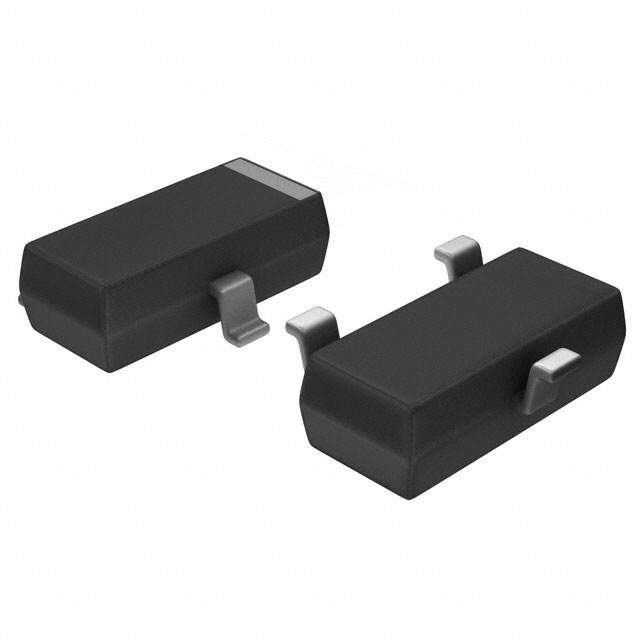
| 描述 | TRANS PREBIAS NPN 200MW MINI3 |
| 产品分类 | 晶体管(BJT) - 单路﹐预偏压式 |
| 品牌 | Panasonic Electronic Components |
| 数据手册 | http://industrial.panasonic.com/www-cgi/jvcr13pz.cgi?E+SC+4+BFA7001+UNR221D+8+WW |
| 产品图片 |
|
| 产品型号 | UNR221D00L |
| rohs | 无铅 / 符合限制有害物质指令(RoHS)规范要求 |
| 产品系列 | - |
| 不同 Ib、Ic时的 Vce饱和值(最大值) | 250mV @ 300µA, 10mA |
| 不同 Ic、Vce 时的DC电流增益(hFE)(最小值) | 30 @ 5mA,10V |
| 产品目录绘图 |
|
| 产品目录页面 | |
| 供应商器件封装 | 迷你型3-G1 |
| 其它名称 | UNR221D00LDKR |
| 功率-最大值 | 200mW |
| 包装 | Digi-Reel® |
| 安装类型 | 表面贴装 |
| 封装/外壳 | TO-236-3,SC-59,SOT-23-3 |
| 晶体管类型 | NPN - 预偏压 |
| 标准包装 | 1 |
| 电压-集射极击穿(最大值) | 50V |
| 电流-集电极(Ic)(最大值) | 100mA |
| 电流-集电极截止(最大值) | 500nA |
| 电阻器-发射极基底(R2)(Ω) | 10k |
| 电阻器-基底(R1)(Ω) | 47k |
| 频率-跃迁 | 150MHz |


- 商务部:美国ITC正式对集成电路等产品启动337调查
- 曝三星4nm工艺存在良率问题 高通将骁龙8 Gen1或转产台积电
- 太阳诱电将投资9.5亿元在常州建新厂生产MLCC 预计2023年完工
- 英特尔发布欧洲新工厂建设计划 深化IDM 2.0 战略
- 台积电先进制程称霸业界 有大客户加持明年业绩稳了
- 达到5530亿美元!SIA预计今年全球半导体销售额将创下新高
- 英特尔拟将自动驾驶子公司Mobileye上市 估值或超500亿美元
- 三星加码芯片和SET,合并消费电子和移动部门,撤换高东真等 CEO
- 三星电子宣布重大人事变动 还合并消费电子和移动部门
- 海关总署:前11个月进口集成电路产品价值2.52万亿元 增长14.8%


PDF Datasheet 数据手册内容提取
This product complies with the RoHS Directive (EU 2002/95/EC). Transistors with built-in Resistor UNR221x Series (UN221x Series) Silicon NPN epitaxial planar type Unit: mm For digital circuits / 0.40+–00..0150 0.16+–00..0160 e 3 ■•CrFeodesutacstt iucoarnne osbfe t hreed nuucmedb ethr roofu pgahr tdso.wnsizing of the equipmenct and d +0.251.50–0.05+0.22.8–0.3 5˚ 0.4±0.2 1 2 •Mini type package allowing easy automatic insertion nthrough tape packing and magazine packing e(0.915.)9±(00.1.95) (0.65) e. a 2.90+–00..0250 ag ■ Resistance by Part Number u st Marking Symboln(R1) (R2) 10˚ cle ••••UUUUNNNNRRRR2222222211110123 ((((UUUUNNNN2222222211110123)))) 8888LABCe24417270 kkkkΩΩΩΩ 124027i kkkΩΩΩ n duct lifecy+0.21.10 to 0.1–0.1 +0.31.1–0.1 123::: ECBmoasliletetcetror •UNR2214 (UN2214)t8D 10 kΩ t47 kΩ ro EIAJ: SC-59 •UNR2215 (UN22n15) 8E 10 kΩn r P Mini3-G1 Package u •UNR2216 (UN2216) 8F 4.7 kΩ oInternal Connection •UNR2217 i(UN2217) 8H o22 kΩ g f pe n. n y o •••••••••••UUUUUUUUUUUMNNNNNNNNNNNRRRRRRRRRRR222222222222222222222211111111111aNVTKDMLFE98 (((((((((((UUUUUUUUUUUDNNNNNNNNNNNi222222222222222222222211111111111NTVMKDLFE98)))))))))))sEEEF8888888QOKINPMDLZXcDisco022444n2144.t1.....5i207727277 1 kn kkkk kkkkkΩkuΩΩΩΩΩΩΩΩΩΩed ipnl24454441112cal....77700022771nu kkkkkkkkkkkedΩΩΩΩΩΩΩΩΩΩΩde pls mamfanaoiillenntotd eewdindiniasasncnccocoenen t ttitgi ynnpuUueeeRddL ttoayynb.ppBopeeuadt nlRRaa12tseosnti ic.ncfoo.rjpCEm/aetin/ •UNR221Z (UN221Z) cFe/F 4.7 kΩ 22 kΩ win mic n o e ■ Absolute Maxinmteunma Ratings Ta = 25°C sit follww.s Paramaieter Symbol Rating vUinit w Collector-base voMltage (Emitter open) V 50 se V p:// CBO ea htt Collector-emitter voltage (Base open) VCEO 5P0l V Collector current I 100 mA C Total power dissipation PT 200 mW Junction temperature T 150 °C j Storage temperature T −55 to +150 °C stg Note) The part numbers in the parenthesis show conventional part number. Publication date: May 2005 SJH00010DED 1
This product complies with the RoHS Directive (EU 2002/95/EC). UNR221x Series ■ Electrical Characteristics T = 25°C ± 3°C a Parameter Symbol Conditions Min Typ Max Unit Collector-base voltage (Emitter open) V I = 10 µA, I = 0 50 V CBO C E Collector-emitter voltage (Base open) V I = 2 mA, I = 0 50 V CEO C B Collector-base cutoff current (Emitter open) I V = 50 V, I = 0 0.1 µA CBO CB E / Collector-emitter cutoff current (Base open) ICEO VCE = 50 V, IB = 0 e 0.5 µA Emitter-base UNR2210/2215/2216/2217 I V = −6 V, I = 0 0.01 mA EBO EB C cutoff current UNR2213 c 0.1 (Collector open) UNR2212/2214/221D/ d 0.2 221E/221M/221N/221T n UNR221Z e 0.4 e. UNR2211 a 0g.5 a UNR221F/221K u st1.0 e UNR2219 n cl 1.5 y UNR2218/221L/221V n c 2.0 e Forward current UNR221V e hFE VCE = 10 V, IC = 5 mA ct l6if 20 transfer ratio UNR2218/221K/221L i u 20 d UNR2219t/221D/221F t o 30 r UNR2n211 n r P 35 u iUNR2212/221E o g fo pe 60 n. UNR221Z n y 60 200 o COOouuMlttlppeuucttt ovvroo-llaettaamggieet tlheUUUUUUDoriNNwNNNNg sRhiR-RRRRa2-lt2e2l2222ue1v22222rv01ea1111*el3/tVDN32li/2o/2/s21n225221 *v1/412Ko/2T2l1t26a*1cg/2MDei21s7*coVnVtVCiEOOn(HLsaut)ed VIVVIViCCpCCCCn l==CCCCca l11====n00u 5555 edmm VVVVdeAA p,,,,ls ,,VVVV mamIIfBBBBBBanao i il======len n1023t01otd0..... e55535e w V dindVVVmmini,as ,,,aAAs RRRRncncLLLLco co ====ene n t 1 tti111tgi k ynkkknΩΩΩΩpuUueeeRddL ttoayynb.pp14ope88e6.00ua9d0t nlaatseosnti ic.ncf0oo440.r.j06.22005pm/aetin/VVV UNR221E ce/ VCC = 5 V, VB = 6 V, RL =wi 1n kΩ mic TInrpaunt sreitsiisotnan fcreequUenNcRyn2t2e18nan RfT1 VCB = 10 V, IE s=it − f2 omllAo, wf =w .2s00e MHz −30% 01.5501 +30% MkΩHz UNaiR2219 vi w 1.0 UMNR221M/211V se p:// 2.2 UNR2216/221F/221L/ ea htt 4.7 Pl 221N/221Z UNR2211/2214/2215/221K 10 UNR2212/2217/221T 22 UNR2210/2213/221D/221E 47 Note)1.Measuring methods are based on JAPANESE INDUSTRIAL STANDARD JIS C 7030 measuring methods for transistors. 2.*:Rank classification Rank Q R S No-rank h 160 to 260 210 to 340 290 to 460 160 to 460 FE 2 SJH00010DED
This product complies with the RoHS Directive (EU 2002/95/EC). UNR221x Series ■ Electrical Characteristics (continued) T = 25°C ± 3°C a Parameter Symbol Conditions Min Typ Max Unit Resistance ratio UNR221M R/R 0.047 1 2 UNR221N 0.1 UNR2218/2219 0.08 0.10 0.12 / UNR221Z e 0.21 UNR2214 0.17 0.21 0.25 UNR221T c 0.47 UNR221F d0.37 0.47 0.57 UNR221V n 1.0 UNR2211/2212/2213/221L e 0.8 1.0 1.2e. UNR221K a 1.70 2.13 a2g.60 UNR221E u 1.70 2.1e4 st2.60 UNR221D n 3.7 c4l.7 5.7 y n c Note)Measuring methods are based on JAPANESE INDUSTRIAL STANDARD JIS C 7030 measurieng methods for transistors. e ct lif Common characteristics chart i u d P Tt t ro 250 T na n r P u o )W 200 i o ng f ype on. (Total power dissipation P mTM1150500000 Amabi4e0nt Dtemip8e0ratures T12a 0 (°Cc)Di16s0continued ipnlcalnuedde pls mamfanaoiillenntotd eewdindiniasasncnccocoenen t ttitgi ynnpuUueeeRddL ttoayynb.ppopeeuadt nlaatseosnti ic.ncfoo.rjpm/aetin/ ce/ win mic Characteristics charts onf UNR2210 o e IC n tVeCnEa VCE(sat) sit fICollww.s hFE IC Collector current I (mA)C 6543200000 IB = 01.M.300 .amm9i 0AmA.8A m0.A7 0m.6A0 .m5T0 aAm. 4=A 0m2.51A° mCA mitter saturation voltage V (V)CE(sat)1010.1100 Please2 5°vCihttpT:/aI /C= /7 wI5B° =C 10 ward current transfer ratio hFE123400000000 Ta = −2V7525C°5°EC°C =C 10 V 10 or-e For ct −25°C e oll 0 C0.01 0 0 2 4 6 8 10 12 0.1 1 10 100 1 10 100 1 000 Collector-emitter voltage VCE (V) Collector current IC (mA) Collector current IC (mA) SJH00010DED 3
This product complies with the RoHS Directive (EU 2002/95/EC). UNR221x Series C V I V V I ob CB O IN IN O (pF)Cob 65 fIT E=a = =1 0 2M5°HCz 104 TVaO = = 2 55 °VC 100 VTaO = = 2 05.°2C V or output capacitancemon base, input open circuited) 4321 µOutput current I (A)O 11100023 nce/Input voltage V (V)INd01.110 ctm Colle (Co 00.1 1 10 100 10a.4 0.6 0.8 1.0 1.2 1.4e0.010.1 1 age.10 100 Collector-base voltage VCB (V) Input voltage VIN (Vu) Outpute cusrtrent IO (mA) n cl y n c e Characteristics charts of UNeR2211 ct lif I V iV I u h I C CE CE(sat) C d FE C Collector current I (mA)CM114286000000Collea2ct0o.ir08I-. Be9m m =4DmA 1iAt.t0ie mr 6vAnoltatg8se 0T .0aV7 .0 =6mC1.0000 5m2E0....A 12345 mA °c(mmmmCAVDAAAAi)12scoontCollector-emitter saturation voltage V (V)iCE(sat)n01u.0010.11100e0.nd1 ipnltCcoalllnuecedt1oder −p lsc2 u5mamf˚rCranaoei2iln5lent°n tCo tdI1 Ce0ew d iInTd(inCima n/ asa= sAI gBnc7nc )5=fcoc° o1Coe0nen 1t tut0itgi0r yn ynpuUpuPreeeeRodForward current transfer ratio hdL FE ttoay1234yn0000b.p00000p1opeeuadt nlCaoatslleeoc1tsno0tir icc.uncrfreoon.rjt 1pIm0C/0 TVa e(−ta2Cmi 25n=E5 /°A o=7°C C5)1n°0.C V1 000 C V ce/ I V win mic V I ob CB n O IN o e IN O (pF)Cob 65 aintenafIT E=a = =1 0 2M5°HCz 104 visit follVTaOw = = 2 w55 °VwC.s 100 VTaO = = 2 05.°2C V or output capacitancemon base, input open circuited) 4321 M µOutput current I (A)O 11100023 Please http:// Input voltage V (V)IN 01.110 ctm Colle (Co 0 1 0.01 0.1 1 10 100 0.4 0.6 0.8 1.0 1.2 1.4 0.1 1 10 100 Collector-base voltage VCB (V) Input voltage VIN (V) Output current IO (mA) 4 SJH00010DED
This product complies with the RoHS Directive (EU 2002/95/EC). UNR221x Series Characteristics charts of UNR2212 I V V I h I C CE CE(sat) C FE C Collector current I (mA)C114286000000IB =0 1.92.0 m0 m.A8A m4A 6 8 Ta0 =.17000000 02 ......m6345125 °mAmmmmmCAAAAAA12 Collector-emitter saturation voltage V (V)CE(sat)01.0010.111000.a1 −n251°C25°Cc10ICT ue/a I=B 7=5/ °1C0100eForward current transfer ratio hFEd12340000000001 10e stage1.00TV−2aC 25=E5° =7C°C5 1°0C V1 000 Collector-emitter voltage VCE (V) n Collector current IC (mA) Colyleccltor current IC (mA) n c e Cob VCB e iIO VIN uct lif VIN IO (pF)Cob 65 ntfIT E=a = =1 0 2M5°HCz 104nt VTaO = = 2 55 °VCur Prod100 VTaO = = 2 05.°2C V Collector output capacitance (Common base, input open circuited) M043210.1Colalectior-1Dbasei voltag1es0 VCB (Vc)D1i0s0coontµOutput current I (A)iOnu1110010e230.d4 ipnlc0alI.6nnupuedt dve0 po.ls8l tmamafganaoieil le1 nVn.t0otdI Neew d ind(iniVn1asas).2gncnc fcocooenen t1 tti.tgi4 ynynpuUpueeeeRdInput voltage V (V)dL IN ttoa0yyn.001b.p.p11100ope.e1uadt nlaOatsuteopusn1tti cicu.rnrcfenoot.r j IOp1m/ 0 (aemtinA/o)n.100 Characteristics charts of cUeN/R2213 win mic n o e Collector current I (mA)C1142860000 IMCIB a=i 1n. 0tV meCAnEa0T0.9a. 08 =m. 000000 7m2A...... 5143625mA °mmmmmmACAAAAAA ctor-emitter saturation voltage V (V)CE(sat)1010.1100 Pl−2e5V°aCsCEe( s2av5ti°)C hsittt fpI:Co/Il/CTl /a wI=B 7=w5 1°C0w.s Forward current transfer ratio hFE123400000000 hFE IC VCTEa−2 ==52 °517C°05C °VC e oll 0 C0.01 0 0 2 4 6 8 10 12 0.1 1 10 100 1 10 100 1 000 Collector-emitter voltage VCE (V) Collector current IC (mA) Collector current IC (mA) SJH00010DED 5
This product complies with the RoHS Directive (EU 2002/95/EC). UNR221x Series C V I V V I ob CB O IN IN O (pF)Cob 65 fIT E=a = =1 0 2M5°HCz 104 VTaO = = 2 55 °VC 100 VTaO = = 2 05.°2C V or output capacitancemon base, input open circuited) 4321 µOutput current I (A)O 11100023 nce/Input voltage V (V)INd01.110 ctm Colle (Co 0 1a e0.01 ge. 0.1 1 10 100 0.4 0.6 0.8 1.0 1.2 1.4 0.1 1 a 10 100 Collector-base voltage VCB (V) Input voltage VIN (Vu) Outpute cusrtrent IO (mA) n cl y n c e Characteristics charts of UNeR2214 ct lif I V iV I u h I C CE CE(sat) C d FE C t t o Collector current I (mA)CM114286000000Collea2ctori-em4DitteiIrB 6v=no 1l.t0a gm8seA T 0Va 0.=09C000000.1 8. ......27E0m162345 5m m Ammmmmm°(cACVAAAAAAADi)12scoontCollector-emitter saturation voltage V (V)iCE(sat)n01u.0010.11100e0.n1d ipnlCcoa−ll2lnu5e°ceCdt1oder p2 lcs5 u°mamfCrranaeoiilnlentn t otdI1 Ce0e w dIind(TCinim an/as a s=AIBgn cnc7 ) =5fcoc o°1Coe0nen1 t t0utitgi0r yn ynpuUpuPreeeeRdForward current transfer ratio hdL FE ttoay1234yn0000b.p00000p1opeeuadt nlCaoatslleeoc1tsno0tir icc.uncrfreoon.rjt 1pIm0C/0 aV e(tCmiTnEa−2 /A o==52 )°5 1n7C°0.5C °V1C 000 C V ce/ I V win mic V I ob CB n O IN o e IN O (pF)Cob 65 aintenafIT E=a = =1 0 2M5°HCz 104 visit folVTlaO w= = 2 5w5 °VCw.s 100 VTaO = = 2 05.°2C V or output capacitancemon base, input open circuited) 4321 M µOutput current I (A)O 11100023 Please http:// Input voltage V (V)IN 01.110 ctm Colle (Co 0 1 0.01 0.1 1 10 100 0.4 0.6 0.8 1.0 1.2 1.4 0.1 1 10 100 Collector-base voltage VCB (V) Input voltage VIN (V) Output current IO (mA) 6 SJH00010DED
This product complies with the RoHS Directive (EU 2002/95/EC). UNR221x Series Characteristics charts of UNR2215 I V V I h I C CE CE(sat) C FE C nt I (mA)C112600 0.0I8B. 9 m= m A1A.0 mA Ta 0=000. 7...2456 5m mmm°ACAAA n voltage V (V)CE(sat)11000 IC e/ IB =/ 10 nsfer ratio hFE340000 TVaC =E 7=5 1°0C V Collector curre 4800 000...123 mmmAAA or-emitter saturatio 0.11 n25°CcTa = 75°C eForward current trad120000 e.−252°5C°C ect a−25°C g 00 2 4 6 8 10 12 Coll0.010.1 1 10 u100 01 10e sta 100 1 000 Collector-emitter voltage VCE (V) n Collector current IC (mA) Coylleccltor current IC (mA) n c e Cob VCB e iIO VIN uct lif VIN IO Collector output capacitance (pF)Cob (Common base, input open circuited) M06543210.1Colalectior-1Dbasei vonltagt1es0 VfITE =a C = =B1 0 2M 5(V°HcC)zD1i0s0coontµiOutput current I (A)Onu1111000e102340n.d4 ipnltc0alI.6nnupuedt dev0 pol.s8l mtamfaganaoieill e1n nV.tot0dI eNew di ndin(iVTVna1saaOs ).= 2gnc=nc 2 fc5oc5o °VoenCen t 1tutitgi.4r yn ynpuUpuPreeeeRodInput voltage V (V)dL IN dtto0ay1y.0n010.b.p11100p0ope.e1uadt nlaOatsuteopusn1tti cicu.rnrcfenoot.r j IOp1m/ 0 (aVTemtaOi nA= =/ o2) 05n.°2.C V100 Characteristics charts of cUeN/R2216 win mic n o e Collector current I (mA)C1142860000 IMC aiIBn t=V e1C.0nE maAT0a0.9 0.=000008 .m 7..... 225634m A5m mmmmmA°CAAAAAA mitter saturation voltage V (V)CE(sat)1010.1100 PleVasCE2e(5 s°avCti) hsittt fpI:Co/TIl/Cla /= wI B7 5=w° C1w0.s ward current transfer ratio hFE123400000000 hFE IC −T2V25aC 5°=EC° C=75 1°0C V or-e For ct 0.1 mA olle −25°C 0 C0.01 0 0 2 4 6 8 10 12 0.1 1 10 100 1 10 100 1 000 Collector-emitter voltage V (V) Collector current I (mA) Collector current I (mA) CE C C SJH00010DED 7
This product complies with the RoHS Directive (EU 2002/95/EC). UNR221x Series C V I V V I ob CB O IN IN O (pF)Cob 65 fIT E=a = =1 0 2M5°HCz 104 VTaO = = 2 55 °VC 100 VTaO = = 2 05.°2C V or output capacitancemon base, input open circuited) 4321 µOutput current I (A)O 11100023 nce/Input voltage V (V)INd01.110 Collect (Com 0 1a e0.01 ge. 0.1 1 10 100 0.4 0.6 0.8 1.0 1.2 1.4 0.1 1 a 10 100 Collector-base voltage VCB (V) Input voltage VIN (Vu) Outpute cusrtrent IO (mA) n cl y n c e Characteristics charts of UNeR2217 ct lif I V iV I u h I C CE CE(sat) C d FE C Collector current I (mA)CM1120864200000000Collea2ctIoBir =-e1m 40D.0.9i tm 0tm.ieA8Ar m06vn.7Ao lm0t.a6Atg 8sme0 A . 5VT m000a0C1 ....A=E03142 2 mmmm(c5V°AAAADCi)12scoontCollector-emitter saturation voltage V (V)iCE(sat)n01u.0010.e111000n.d1 ipnltCcaollnlue−ce2dt51ode°r Cp l2sc 5umamf°rCarnaoieilnlentnt ot dI1 eCe0w TdiI ndin(aCi m =na/sa s IA7gBncn5c )=°fcocC o1oen0en 1t tuti0tgir0 yn ynpuUpuPreeeeRoForward current transfer ratio hddL FE ttoay1234yn0000b.p00000p1opeeuadt nlCaoaltsleeoc1tsno0tir icc.unrcfreoon.rtj 1Ipm0C/0 −T2V ae2(5atC m5°i=EnC° A/C7=o5 )1°n0C. V1 000 C V ce/ I V win mic V I ob CB n O IN o e IN O or output capacitance (pF)Cobmon base, input open circuited) 654321 MaintenafIT E=a = =1 0 2M5°HCz µOutput current I (A)O 11110000234 Please vihsittt fp:o/l/lVTaOw = = 2 w55 °VwC.s Input voltage V (V)IN1010.1100 VTaO = = 2 05.°2C V ctm Colle (Co 0 1 0.01 0.1 1 10 100 0.4 0.6 0.8 1.0 1.2 1.4 0.1 1 10 100 Collector-base voltage VCB (V) Input voltage VIN (V) Output current IO (mA) 8 SJH00010DED
This product complies with the RoHS Directive (EU 2002/95/EC). UNR221x Series Characteristics charts of UNR2218 I V V I h I C CE CE(sat) C FE C Collector current I (mA)C22114062800000 IB = 1.00. 9m 0mA.8TA a0m .=7A000 2...m4565 A°mmmCAAA mitter saturation voltage V (V)CE(sat)1010.1100 n25°CcTIaC e=/ I7B5 =°/C 10 ward current transfer ratio hFEd1148260000 Ta−2V =25C5 °7EC° 5C=° C10 V 40 0.3 mA or-e eFor e. 00 2 4 6 8 1000..12 mmAA12 Collect0.010a.1 −25°C1 10 u100 01 10e stag100 1 000 Collector-emitter voltage VCE (V) n Collector current IC (mA) Coylleccltor current IC (mA) n c e Cob VCB e iIO VIN uct lif VIN IO Collector output capacitance (pF)Cob (Common base, input open circuited) M06543210.1Colalectior-1Dbasei vonltagt1es0 VfIT E=a C = =B1 0 2M (5V°HcC)zDi10s0coontµOutput current I (A)iOnu1111000e102340n.d4 ipnltc0alI.6nnupuedt dev0 po.ls8l mtamfaganaoieil le1 nnV.to0tdI Neew di nd(inVTiVna1asOas ).= 2gn=cn c 2 5fco5co °VoeCnen t1 tutit.gi4r yn ynpuUpuPreeeeRodInput voltage V (V)dL IN dtto0ay1y0.n100.b.p11001p0op.ee1uadt nlaOatsuteopusn1tti cicu.rnrcfenoot.r j IOp1m /0 (TVaemtaOi An= =/ o2) 05.n°2.C V100 Characteristics charts of cUeN/R2219 win mic n o e Collector current I (mA)C22114062800000 IB =I 1MC0.0. a9 im 0m.A8nA tm0V.e7AC mn0E.A6a mTAa = 0002...5345° mmmCAAA mitter saturation voltage V (V)CE(sat)1010.1100 PleVasCEe2( s5av°tiC) hsittt fpI:Co/IlT/Cla / = wI B7 =5w° 1C0w.s ward current transfer ratio hFE 1148260000 hFE ICT−2Va2 5=C5°E C°7 C=5 °1C0 V 40 0.2 mA or-e For ct 0.1 mA olle −25°C 0 C0.01 0 0 2 4 6 8 10 12 0.1 1 10 100 1 10 100 1 000 Collector-emitter voltage V (V) Collector current I (mA) Collector current I (mA) CE C C SJH00010DED 9
This product complies with the RoHS Directive (EU 2002/95/EC). UNR221x Series C V I V V I ob CB O IN IN O (pF)Cob 65 fITE =a = =1 0 2M5°HCz 104 VTaO = = 2 55 °VC 100 VTaO = = 2 05.°2C V or output capacitancemon base, input open circuited) 4321 µOutput current I (A)O 11100023 nce/Input voltage V (V)INd01.110 Collect (Com 0 1a e0.01 ge. 0.1 1 10 100 0.4 0.6 0.8 1.0 1.2 1.4 0.1 1 a 10 100 Collector-base voltage VCB (V) Input voltage VIN (Vu) Outpute cusrtrent IO (mA) n cl y n c e Characteristics charts of UNeR221D ct lif I V iV I u h I C CE CE(sat) C d FE C t t o Collector current I (mA)CM3221100505050CIBo =l l1e.a20c tmoAri-0e.60m4 D.m7i0 Atm.t8eiA mr0 6vA.n9o mltAa0g.85se 0 m T. 4AVa m0=C1.A 300E02 ..m 512 ° (cAmmCVDAAi)12scoontCollector-emitter saturation voltage V (V)iCE(sat)n01u.0010.11100e0.n1d ipnlCcoall−lnue2c5edt°1oCder p2 lcs5 u°mamfCrranaeoiilnlentn to tdI1 Ce0ew TdiInd(inCaim n/a=sa sAI gB7ncnc )5=fc°oc oC1oe0nen1 t tut0itgi0r yn ynpuUpuPreeeeRdForward current transfer ratio hdL FE ttoay11yn4826b.p00000p1opeeVuadCtE n lC=a oa1tsl0l eVeoc1tsno0tir icc.uncrfreoon.rjt 1pIm0/C0 Ta 2−e(ta52mi n°=5C/A° o7C5)n°.C1 000 C V ce/ I V win mic V I ob CB n O IN o e IN O or output capacitance (pF)Cobmon base, input open circuited) 654321 MaintenafIT E=a = =1 0 2M5°HCz µOutput current I (A)O 11110000234 Please vihsittt fp:o/l/VTlaO w= = 2 5w5 °VCw.s Input voltage V (V)IN1010.1100 VTaO = = 2 05.°2C V ctm Colle (Co 0 1 0.01 0.1 1 10 100 1.5 2.0 2.5 3.0 3.5 4.0 0.1 1 10 100 Collector-base voltage VCB (V) Input voltage VIN (V) Output current IO (mA) 10 SJH00010DED
This product complies with the RoHS Directive (EU 2002/95/EC). UNR221x Series Characteristics charts of UNR221E I V V I h I C CE CE(sat) C FE C Collector current I (mA)C 6543200000 0.08. 9m mAIBA = 1.0 0m0.5.6A 0m m.04AA. 7m0 .m3A AmAT0a 0.=1.2 2m m5A°AC mitter saturation voltage V (V)CE(sat)1010.1100 n25°CcTIaC =e/ I7B5 =°/C 10 ward current transfer ratio hFEd1148260000 2−TV52aC °5=EC° =C7 51°0C V 10 or-e eFor e. 00 2 4 6 8 10 12 Collect0.010a.1 −251°C 10 u100 01 10e stag100 1 000 Collector-emitter voltage V (V) n Collector current I (mA) Colleccltor current I (mA) CE C y C n c e Cob VCB e iIO VIN uct lif VIN IO Collector output capacitance (pF)Cob (Common base, input open circuited) M06543210.1Colalectior-1Dbasei vnoltagt1es0 VfIT E=aC = =B1 0 M2 (5HV°cCz)Di10s0coontµOutput current I (A)iOnu111100010e2341.nd5 ipnltc2alI.0nnupuedt dve2 po.ls5l tmamafganaoieil le3 nVn.t0otdI Neew d ind(VTiniVanO3as as= ).=5gn cn2c 55fco co°VCoenen t4 tuti.tgi0r yn ynpuUpuPreeeeRodInput voltage V (V)dL IN dttoa0y1yn0.100b.p.p110010ope.e1uadt nlaOatsuteopusn1tti cicu.rnrcfenoot.r j IOp1m/ 0 (aVTemtaiO nA= =/o )2 05n.°2.C V100 Characteristics charts of cUeN/R221F win mic n o e Collector current I (mA)C2211406284000000 IB = 1.0 mAIMC ain0 t.V6e m0C.nA7E 0am.T8A am =0000A ....295345 mmmm°CAAAA or-emitter saturation voltage V (V)CE(sat)1010.1100 PleVasCEe2( 5s°avCti) hsittt fpI:Co/ITl/Cla /= wI B7 5=w° 1Cw0.s Forward current transfer ratio hFE1148260000 hFE IC 2−TV52aC °5=EC° =C7 51°0C V 00..12 mmAA ollect −25°C 0 C0.01 0 0 2 4 6 8 10 12 0.1 1 10 100 1 10 100 1 000 Collector-emitter voltage VCE (V) Collector current IC (mA) Collector current IC (mA) SJH00010DED 11
This product complies with the RoHS Directive (EU 2002/95/EC). UNR221x Series C V I V V I ob CB O IN IN O (pF)Cob 65 fIT E=a = =1 0 2M5°HCz 104 VTaO = = 2 55 °VC 100 VTaO == 205.2°C V or output capacitancemon base, input open circuited) 4321 µOutput current I (A)O 11100023 nce/Input voltage V (V)INd01.110 Collect (Com 0 1a e0.01 ge. 0.1 1 10 100 0.4 0.6 0.8 1.0 1.2 1.4 0.1 1 a 10 100 u st Collector-base voltage VCB (V) Input voltage VIN (V) Outpute current IO (mA) n cl y n c e Characteristics charts of UNeR221K ct lif I V iV I u h I C CE CE(sat) C d FE C t t o Collector current I (mA)CM221140628400000000Collea2ctori-em4Dittier 6vnoltag8seI BT Va= = C1010001 0E2......228460 5 °mmmmmm(cCVDAAAAAAi1)2scoontCollector-emitter saturation voltage V (V)iCE(sat)n01u.0010.11100e1nd ipnlCcaollnlu2e5ced1°tCo0der p lscT −umaamf 2r=ra5 naoei7°ilnC5lent°n tCot d1I 0eCew0 di Ind(inCim na/sa sAIgBncnc )=fcoco 1oen01en t 0tutitgi0r y0n ynpuUpuPreeeeRdForward current transfer ratio hdL FE ttoay2211yn406284b.p0000000p1opeeuadt nlCaaotslleeoc21stTn5o0tia°r C= icc .7un5crf°r−Ceoo2n.r5jt° C1pIm0/C0 Va e(tCmiEn /A=o )1n0. V1 000 C V ce/ V I win mic ob CB n IN O o e (pF)Cob 65 aintenafIT E=a = =1 0 2M5°HCz 100 visit foVTllaO = =w 2 05.w°2C Vw.s or output capacitancemon base, input open circuited) 4321 M Input voltage V (V)IN 01.101 Please http:// ctm Colle (Co 0 0.01 1 10 100 0.1 1 10 100 Collector-base voltage V (V) Output current I (mA) CB O 12 SJH00010DED
This product complies with the RoHS Directive (EU 2002/95/EC). UNR221x Series Characteristics charts of UNR221L I V V I h I C CE CE(sat) C FE C Collector current I (mA)C22114062800000 ITB a= = 1000 2....08645 °mmmmCAAAA mitter saturation voltage V (V)CE(sat)1010.1100 n25°TCa = 7c5°C IC e/ IB =/ 10 ward current transfer ratio hFEd22114062800000 25T°aC = 75°C−25°C VCE = 10 V 4000 2 4 6 8 100.2 mA12 Collector-e0.011a 10−25°C 100 u1 00e0 For 4001 10e stage1.00 1 000 Collector-emitter voltage VCE (V) n Collector current IC (mA) Coylleccltor current IC (mA) n c e Cob VCB e iVIN IO uct lif Collector output capacitance (pF)Cob (Common base, input open circuited) M06543211 Colalectior-Dbasei v10onltagtes fITVE =a C = =1B 0 2 M 5(°VHCcz)D1i0s0coontInput voltage V (V)iINn01u.0010.11100e0.nd1 ipnltcOalunutpedu1tde cplsu rmamfreanaoniiltle n nItotdO1 e 0e w(dTVinmdiniaO naA= sas= g)2 nc0nc 5.fc°2ocoC Voenen 1t tuti0tgir0 yn ynpuUpuPreeeeRoddL dttoayynb.ppopeeuadt nlaatseosnti ic.ncfoo.rjpm/aetin/on. Characteristics charts of cUeN/R221M win mic n o e Collector current I (mA)C22114062800000 IBI MC= a1i.00. n9m t0 mVA.8eA0 Cm.n7EA 0ma.6AT ma =A0000 ....223455 mmmm°CAAAA mitter saturation voltage V (V)CE(sat)0.001.1110 Ple−2Va5˚sC2C5Ee°( CsavtiT) ahs it=tt 7 5fpI°:CCo/Il/Cl / wIB =w 10w.s ward current transfer ratio hFE235400000000 hFE IC T2−V5a2C °5=EC° =7C5 1°0C V 40 0.1 mA or-e For 100 ct e oll 0 C0.001 0 0 2 4 6 8 10 12 1 10 100 1 000 1 10 100 1 000 Collector-emitter voltage VCE (V) Collector current IC (mA) Collector current IC (mA) SJH00010DED 13
This product complies with the RoHS Directive (EU 2002/95/EC). UNR221x Series C V I V V I ob CB O IN IN O (pF)Cob 5 fIT E=a = =1 0 2M5°HCz 104 VTaO = = 2 55 °VC 100 VTaO = = 2 05.°2C V or output capacitancemon base, input open circuited) 4321 µOutput current I (A)O 11100023 nce/Input voltage V (V)INd01.110 Collect (Com 00.1Collector-1base voltag1e0 VCB (V)100 10a.4 0I.6nput v0o.8ltage 1 V.0IN (uV1).2 1.4e0.010.1 Outpu1te cusrtreantg IeO1. 0 (mA) 100 n cl y n c e Characteristics charts of UNeR221N ct lif I V iV I u h I C CE CE(sat) C d FE C Collector current I (mA)CM114286000000Collea2ctori-em4Dittier 6vnoltatg8se IT B Va= = C11 20E.00000000005 .........248769531 °(mc CmmmmmmmmmVDAAAAAAAAAAi1)2scoontCollector-emitter saturation voltage V (V)iCE(sat)n0u.001.e11101nd 2i5p°nlt−CC2cTaol5al° nl=Cue c7ed15t0o°deCr p lsc umamfrranaoeiilnlentn tot 1dI 0eCe0w di Ind(inCim na/sa sIAgBncnc )=fcoc o1oe1n0en t 0tutit0gir 0yn ynpuUpuPreeeeRodForward current transfer ratio hdL FE ttoay44321yn802468b.p0000000p1opeeuadt nlC2a5oa°tslCleeoc1tsno0tir T icc.au n=−crf 2r75eo5o°n.°rCjtC 1pIm0C/0 Va e(tCminE /Ao= )1n0. V1 000 C V ce/ I V win mic V I ob CB n O IN o e IN O (pF)Cob 65 aintenafIT E=a = =1 0 2M5°HCz 104 visit folVTlaO w= = 2 w55 °VCw.s 100 VTaO = = 2 05.°2C V or output capacitancemon base, input open circuited) 4321 M µOutput current I (A)O 11100023 Please http:// Input voltage V (V)IN 01.110 ctm Colle (Co 0 1 0.01 1 10 100 0.4 0.6 0.8 1.0 1.2 1.4 0.1 1 10 100 Collector-base voltage V (V) Input voltage V (V) Output current I (mA) CB IN O 14 SJH00010DED
This product complies with the RoHS Directive (EU 2002/95/EC). UNR221x Series Characteristics charts of UNR221T I V V I h I C CE CE(sat) C FE C Collector current I (mA)C1142860000 TIaB == 21000000005.........078965432° CmmmmmmmmmAAAAAAAAA mitter saturation voltage V (V)CE(sat) 01.110 25°CTa =n 75°C cICe / IB =/ 10 ward current transfer ratio hFEd443218024600000 25°C T−a 2=5 7°5C°C VCE = 10 V 0.1 mA or-e eFor 80 e. 0 Collect0.01a−25°C u 0 stag 0 2 4 6 8 10 12 1 10 100 1 000 1 10e 100 1 000 Collector-emitter voltage VCE (V) n Collector current IC (mA) Coylleccltor current IC (mA) n c e IO VIN e iIO VIN uct lif VIN IO (pF)Cob 65 ntfIT E=a = =1 0 2M5°HCz 104nt TVaO = = 2 55 °VCur Prod100 VTaO = = 2 05.°2C V Collector output capacitance (Common base, input open circuited) M043211 Colalectior-Dbasei v10oltages VCB (Vc)Di10s0coontµiOutput current I (A)Onu11100e10230.d4 ipnlc0alI.6nnupuedt dev 0pol.s8l mtamfaganaoieill e1n nV.tot0dI eNew di ndin(iVna1sas.)2gncnc fcocooenen t 1ttitgi.4 ynynpuUpueeeeRdInput voltage V (V)dL IN tto0ayyn.001b..p1110p0ope.e1uadt nlaOatsuteopusn1tti cicu.rnrcfenoot.r j IOp1m/ 0 (aemtinA/o)n.100 Characteristics charts of cUeN/R221V win mic n o e Collector current I (mA)C1142860000 IMC ain tVeCnEaTIBa == 1200000.05.....78965 °m mmmmmCAAAAAA mitter saturation voltage V (V)CE(sat) 01.110 PleVa2sC5TEe°a(C s=av t7i)5 hs°itCtt fpI:Co/Il/Cl / wIB w= 1w0.s ward current transfer ratio hFE22114062800000 h2T5aF° =EC 75°C IC VCE = 10 V 0.4 mA or-e −25°C For 40 −25°C ct e 0 00..32 mmAA Coll0.01 0 0 2 4 6 8 10 12 1 10 100 1 000 1 10 100 1 000 Collector-emitter voltage VCE (V) Collector current IC (mA) Collector current IC (mA) SJH00010DED 15
This product complies with the RoHS Directive (EU 2002/95/EC). UNR221x Series C V I V V I ob CB O IN IN O (pF)Cob 65 fIT E=a = =1 0 2M5°HCz 104 TVaO = = 2 55 °VC 100 VTaO = = 2 05.°2C V d) 103 10 or output capacitancemon base, input open circuite 4321 µOutput current I (A)O 11002 nce/Input voltage V (V)INd0.11 Collect (Com 0 1a e0.01 ge. 1 10 100 0.4 0.6 0.8 1.0 1.2 1.4 0.1 1 a 10 100 Collector-base voltage VCB (V) Input voltage VIN (Vu) Outpute cusrtrent IO (mA) n cl y n c e Characteristics charts of UNeR221Z ct lif I V iV I u h I C CE CE(sat) C d FE C Collector current I (mA)CM114286000000Collea2ctoir-e4mDittier 6vnoltatg8se T I BaV ==C1 120E000000000.5 ....0.....214378965 ° c( mCmmmmmmmmmVDAAAAAAAAAAi1)2scoontCollector-emitter saturation voltage V (V)iCE(sat)n0u.001.1110e1nd ipnltCcaollnluec2edT15to0a°de Cr =−p ls c27 u5m5amf°r°CraCnaoeiilnlentn tot d1I 0eCew0 di nId(inCim na/sas AIgnBcnc ) =fcoco 1oen1e0n t 0tutitgi0r y0n ynpuUpuPreeeeRodForward current transfer ratio hdL FE ttoay44321yn802468b.p0000000p1opeeuadt nlCaaotslleeoc1stno0tir T icc.au n=crf− r72e2oo55n5.°rj°°tCC C 1pIm0/C0 Va e(tCminE /Ao= )1n0. V1 000 C V ce/ I V win mic V I ob CB n O IN o e IN O (pF)Cob 65 aintenafIT E=a = =1 0 2M5°HCz 104 visit folVTlaO w= = 2 w55 °VCw.s 100 VTaO = = 2 05.°2C V or output capacitancemon base, input open circuited) 4321 M µOutput current I (A)O 11100023 Please http:// Input voltage V (V)IN 01.110 ctm Colle (Co 0 1 0.01 1 10 100 0.4 0.6 0.8 1.0 1.2 1.4 0.1 1 10 100 Collector-base voltage V (V) Input voltage V (V) Output current I (mA) CB IN O 16 SJH00010DED
Request for your special attention and precautions in using the technical information and semiconductors described in this book (1)(cid:9)If any of the products or technical information described in this book is to be exported or provided to non-residents, the laws and regulations of the exporting country, especially, those with regard to security export control, must be observed. (2)(cid:9)The technical information described in this book is intended only to show the main characteristics and application circuit examples of the products, and no license is granted under any intellectual property right or other right owned by our company or any other company. Therefore, no responsibility is assumed by our company as to the infringement upon any such right owned by any other company which may arise as a result of the use of technical information described in this book. (3)(cid:9)The products described in this book are intended to be used for standard applications or general electronic equipment (such as office / equipment, communications equipment, measuring instruments and household appliances). Consult our sales staff in advance for information on the following applicateions: (cid:150) Special applications (such as for airplanes, aerospace, automobiles, traffic control equipment, combustion equipment, life support systems and safety devices) in which exceptional quality and reliability are required, or if the failure or malfunction of the prod- c ucts may directly jeopardize life or harm the human body. (cid:150) Any applications other than the standard applications intended. d n (4)(cid:9)The products and product specifications described in this book are subject to change without notice for modification and/or im- e provement. At the final stage of your design, purchasing, or use of the products, therefore, ask for the most upe-t.o-date Product Standards in advance to make sure that the latest spaecifications satisfy your requirements. ag u st (5)(cid:9)When designing your equipment, comply with the range of absolute maximum rating and the guarantee ed operating conditions (operating power supply voltage and opernating environment etc.). Especially, please be careful not to yexclceed the range of absolute maximum rating on the transient state, such as power-on, power-onff and mode-switching. Otherwiseec, we will not be liable for any (cid:9) dEevfeecnt wwhheicnh t hmea pyr aordiusec tlsa taerre i nu syeodeu wr eitqhuinip tmhee ngt.uaranteed values, take into the consideration ocf ti nlicfidence of break down and failure i u mode, possible to occur to semiconductor products. Measures on the systems such as redudndant design, arresting the spread of fire or preventing glitch are retcommended in order to prevetnt physical injury, fire, social damoages, for example, by using the products. r n n r P (6)(cid:9)Comply with the instructions for use in order to prevent breakdown and characteruistics change due to external factors (ESD, EOS, o tdhaemrmp-apl rostorfe spisa caknidn gm iesc rheaqnuiicraeld s, tsraetsiss)f ya tt hteho ec otinmdiet ioofn sh, asnudclhin ags, smheoluf nlitfine ga nodnr gtah tfe c eulsatpoysmepdeer t'sim per oscinecsse. fWirsht eonp eunsiinngg tphreo dpuaccktsa ogfoenrs. .which (7)(cid:9)TEMhleics trbioc oIkna dmusatyriD abl eCi noo.,t Lrtedps.rinted coDri srecproondtuicnedu ewdh ietpnhlecalr nuwedhdoe pllsly mamf aonaoiilrl ennptotda erewtdinidinaialsaslyncnc,c ocowenen ti tttitgih ynonupuUute eeRthddL e t topayynrb.pipoopere uadwt nrliatattseneo spntie ricm.ncfisoso.irjonpm/ oaetfi nM/atsushita ce/ win mic n o e ntena sit follww.s ai vi w M se p:// ea htt Pl