
 Datasheet下载
- 型号: UCLAMP3311P.TCT
- 制造商: SEMTECH
- 库位|库存: xxxx|xxxx
- 要求:
| 数量阶梯 | 香港交货 | 国内含税 |
| +xxxx | $xxxx | ¥xxxx |
查看当月历史价格
查看今年历史价格
UCLAMP3311P.TCT产品简介:
ICGOO电子元器件商城为您提供UCLAMP3311P.TCT由SEMTECH设计生产,在icgoo商城现货销售,并且可以通过原厂、代理商等渠道进行代购。 UCLAMP3311P.TCT价格参考¥1.77-¥1.77。SEMTECHUCLAMP3311P.TCT封装/规格:TVS - 二极管, 。您可以下载UCLAMP3311P.TCT参考资料、Datasheet数据手册功能说明书,资料中有UCLAMP3311P.TCT 详细功能的应用电路图电压和使用方法及教程。
Semtech Corporation 的 UCLAMP3311P.TCT 是一款瞬态电压抑制(TVS)二极管,主要用于保护电子电路免受过电压事件(如静电放电 ESD、电快速瞬变 EFT 和雷击浪涌)的损害。以下是该型号的应用场景:

 1. 消费电子产品
   - 手机和移动设备:用于保护耳机插孔、USB 接口、充电端口等易受 ESD 影响的部分。
   - 电视和显示器:保护 HDMI、USB、音频/视频接口等信号线,防止外部干扰和电压波动。
   - 音频设备:保护音频输入/输出端口,确保音质稳定。

 2. 通信设备
   - 网络设备:如路由器、交换机中的以太网端口保护,防止数据传输过程中因过电压导致损坏。
   - 光纤模块:保护高速数据接口,避免信号中断或硬件故障。
   - 无线通信设备:如 Wi-Fi 模块、蓝牙模块等,防止射频信号受到外界干扰。

 3. 汽车电子
   - 车载信息娱乐系统:保护触摸屏、USB 接口、摄像头接口等。
   - 传感器系统:如倒车雷达、胎压监测系统(TPMS),防止环境中的电磁干扰。
   - 车载网络接口:如 CAN 总线、LIN 总线,提供可靠的过电压保护。

 4. 工业自动化
   - 传感器接口:保护工业传感器免受恶劣环境下的电压波动影响。
   - PLC 控制器:保护输入/输出端口,确保工业控制系统的稳定性。
   - 通信接口:如 RS-232、RS-485 等接口,防止长距离信号传输中的浪涌冲击。

 5. 医疗设备
   - 便携式医疗设备:如血压计、血糖仪,保护 USB 或蓝牙接口。
   - 大型医疗设备:如 X 光机、超声波设备,保护其高灵敏度的信号输入端口。

 6. 物联网(IoT)设备
   - 智能家居设备:如智能灯泡、智能插座,保护无线通信模块和电源接口。
   - 可穿戴设备:如智能手表、健身追踪器,保护其小型化接口免受 ESD 损害。

 特点与优势
- 低电容设计:适合高速数据线路保护,不影响信号完整性。
- 高响应速度:能够快速抑制瞬态电压,保护敏感元件。
- 小封装尺寸:适合空间受限的应用场合。
- 高可靠性:满足多种国际标准(如 IEC 61000-4-2、 MIL-STD-883),适用于严苛环境。

综上所述,UCLAMP3311P.TCT 广泛应用于需要高可靠性和高性能保护的电子设备中,尤其适合对信号完整性和抗干扰能力要求较高的场景。
| 参数 | 数值 |
| 产品目录 | |
| 描述 | TVS DIODE 3.3VWM 18VC 2SLP |
| 产品分类 | |
| 品牌 | Semtech |
| 数据手册 | |
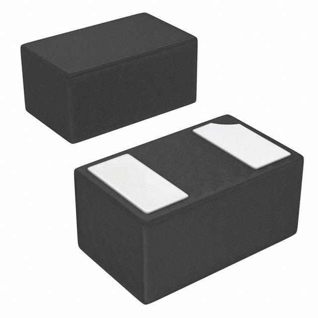
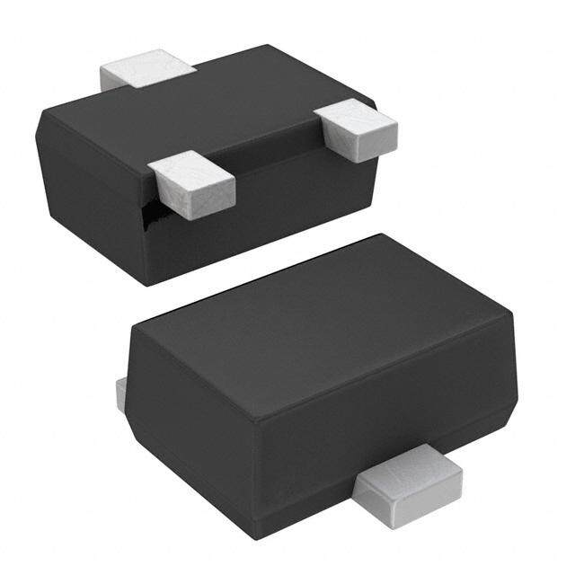
| 产品图片 |
|
| 产品型号 | UCLAMP3311P.TCT |
| rohs | 无铅 / 符合限制有害物质指令(RoHS)规范要求 |
| 产品系列 | uClamp™ |
| 不同频率时的电容 | 12pF @ 1MHz |
| 产品目录页面 | |
| 供应商器件封装 | SLP1006P2 |
| 其它名称 | UCLAMP3311PDKR |
| 功率-峰值脉冲 | 90W |
| 包装 | Digi-Reel® |
| 单向通道 | - |
| 双向通道 | 1 |
| 安装类型 | 表面贴装 |
| 封装/外壳 | 0402(1006 公制) |
| 工作温度 | -40°C ~ 85°C (TJ) |
| 应用 | 通用 |
| 标准包装 | 1 |
| 电压-击穿(最小值) | 3.5V |
| 电压-反向关态(典型值) | 3.3V (最小值) |
| 电压-箝位(最大值)@Ipp | 18V |
| 电流-峰值脉冲(10/1000µs) | 5A (8/20µs) |
| 电源线路保护 | 无 |
| 类型 | 齐纳 |


- 商务部:美国ITC正式对集成电路等产品启动337调查
- 曝三星4nm工艺存在良率问题 高通将骁龙8 Gen1或转产台积电
- 太阳诱电将投资9.5亿元在常州建新厂生产MLCC 预计2023年完工
- 英特尔发布欧洲新工厂建设计划 深化IDM 2.0 战略
- 台积电先进制程称霸业界 有大客户加持明年业绩稳了
- 达到5530亿美元!SIA预计今年全球半导体销售额将创下新高
- 英特尔拟将自动驾驶子公司Mobileye上市 估值或超500亿美元
- 三星加码芯片和SET,合并消费电子和移动部门,撤换高东真等 CEO
- 三星电子宣布重大人事变动 还合并消费电子和移动部门
- 海关总署:前11个月进口集成电路产品价值2.52万亿元 增长14.8%


PDF Datasheet 数据手册内容提取
uClamp3311P Low Voltage µClampTM for ESD and CDE Protection PPRROOTTEECCTTIIOONN PPRROODDUUCCTTSS - MicroClampTM Description Features The µClampTM series of Transient Voltage Suppressors (cid:139) Transient protection for data lines to (TVS) are designed to replace multilayer varistors IEC 61000-4-2 (ESD) ±15kV (air), ±8kV (contact) (MLVs) in portable applications where low operating IEC 61000-4-4 (EFT) 40A (tp = 5/50ns) voltage is vital. They offer superior electrical characteris- Cable Discharge Event (CDE) tics such as lower clamping voltage and no device (cid:139) Ultra-small package (1.0 x 0.6 x 0.5mm) degradation when compared to MLVs. They are de- (cid:139) Protects one data line signed to protect sensitive semiconductor components (cid:139) Low clamping voltage from damage or upset due to electrostatic discharge (cid:139) Working voltage: 3.3V (ESD), lightning, electrical fast transients (EFT), and (cid:139) Low leakage current cable discharge events (CDE). (cid:139) Solid-state silicon-avalanche technology The µClampTM3311P is constructed using Semtech’s proprietary EPD process technology. The EPD process Mechanical Characteristics provides low standoff voltages with significant reduc- (cid:139) SLP1006P2 package tions in leakage currents and capacitance over silicon- (cid:139) RoHS/WEEE Compliant avalanche diode processes. They feature a true (cid:139) Nominal Dimensions: 1.0 x 0.6 x 0.5 mm operating voltage of 3.3 volts for superior protection when compared to traditional pn junction devices. (cid:139) Lead Finish: NiPdAu The µClampTM3311P is in an 2-pin, RoHS/WEEE compli- (cid:139) Molding compound flammability rating: UL 94V-0 ant, SLP1006P2 package. It measures 1.0 x 0.6 x (cid:139) Marking : Marking code, cathode band 0.5mm. The leads are spaced at a pitch of 0.65mm (cid:139) Packaging : Tape and Reel and are finished with lead-free NiPdAu. Each device Applications will protect one line operating at 3.3 volts. It gives the designer the flexibility to protect single lines in applica- (cid:139) Cellular Handsets & Accessories tions where arrays are not practical. They may be used (cid:139) Notebooks & Handhelds to meet the ESD immunity requirements of IEC 61000- (cid:139) Portable Instrumentation 4-2, Level 4 (±15kV air, ±8kV contact discharge). The (cid:139) Digital Cameras combination of small size and high ESD surge capability (cid:139) Peripherals makes them ideal for use in portable applications such (cid:139) MP3 Players as cellular phones, digital cameras, and MP3 players. Dimensions Schematic & PIN Configuration 1.0 0.60 0.65 0.50 Maximum Dimensions (mm) SLP1006P2 (Bottom View) Revision 08/22/2007 1 www.semtech.com
uClamp3311P PROTECTION PRODUCTS Absolute Maximum Rating Rating Symbol Value Units PeakPulsePower(tp =8/20µs) P 90 Watts pk MaximumPeakPulseCurrent (tp =8/20µs) I 5 Amps pp ESDperIEC61000-4-2 (Air) V +/- 25 kV ESD ESDperIEC61000-4-2 (Contact) +/- 20 Operating Temperature T -40to+85 °C J StorageTemperature T -55to+150 °C STG Electrical Characteristics (T=25oC) Parameter Symbol Conditions Minimum Typical Maximum Units ReverseStand-OffVoltage V 3.3 V RWM Punch-Through Voltage V I = 2µA 3.5 V PT PT Snap-BackVoltage V I = 50mA 2.8 V SB SB ReverseLeakageCurrent I V = 3.3V 0.05 0.5 µA R RWM Clamping Voltage V I = 1A,tp = 8/20µs 8 V C PP Clamping Voltage V I = 5A,tp = 8/20µs 18 V C PP I/O pin toGnd 12 15 pF Junction Capacitance C V = 0V,f= 1MHz j R I/O pin toGnd 10 pF V = 3.3V,f= 1MHz R 2007 Semtech Corp. 2 www.semtech.com
uClamp3311P PROTECTION PRODUCTS Typical Characteristics Non-Repetitive Peak Pulse Power vs. Pulse Time Power Derating Curve 110 10 100 90 wer - P (kW)PP 1 d Power or IPP 56780000 o e e P Rat 40 Puls 0.1 % of 30 ak 20 e P 10 0 0.01 0 25 50 75 100 125 150 0.1 1 10 100 1000 Ambient Temperature - T (oC) A Pulse Duration - tp (us) Clamping Voltage vs. Peak Pulse Current Normalized Capacitance vs. Reverse Voltage 20 1.4 18 1.2 V) 16 oltage - V (C 111024 CJ(VR=0)0.81 amping V 68 Waveform CJ(VR) / 00..46 Cl 4 Parameters: tr = 8µs 0.2 2 td = 20µs f = 1 MHz 0 0 0 1 2 3 4 5 6 0 0.5 1 1.5 2 2.5 3 3.5 Peak Pulse Current - IPP (A) Reverse Voltage - VR (V) Insertion Loss S21 CH1 S21 LOG 6 dB / REF 0 dB 1: -3.0120 dB 616.229 MHz 2: -3.8355 dB 0 dB 900 MHz -1-26 ddBB 1 2 3 4 3 : -15.8.9 G80H4z d B 4: -8.1629 dB 2.5 GHz -18 dB -24 dB -30 dB -36 dB 1 10 100 1 3 MHz MHz MHz GHz GHz START . 030 MHz STOP 3 000. 0000 00 MHz 2007 Semtech Corp. 3 www.semtech.com
uClamp3311P PROTECTION PRODUCTS Applications Information Device Connection Options Device Schematic & Pin Configuration The µClamp3311P is designed to protect one data line operating up to 3.3 volts. It will present a high impedance to the protected line up to 3.3 volts. It will “turn on” when the line voltage exceeds 3.5 volts. The device is bidirectional and may be used on lines where the signal polarity is above and below ground. These devices are not recommended for use on dc power supply lines due to their snap-back voltage characteristic. EPD TVS Characteristics These devices are constructed using Semtech’s proprietary EPD technology. The structure of the EPD TVS is vastly different from the traditional pn-junction devices. At voltages below 5V, high leakage current and junction capacitance render conventional ava- lanche technology impractical for most applications. EPD TVS IV Characteristic Curve However, by utilizing the EPD technology, these devices can effectively operate at 3.3V while maintaining excellent electrical characteristics. IPP The EPD TVS employs a complex nppn structure in contrast to the pn structure normally found in tradi- ISB tional silicon-avalanche TVS diodes. The EPD mecha- nism is achieved by engineering the center region of the device such that the reverse biased junction does IPT not avalanche, but will “punch-through” to a conduct- VF IR VRWM VSBVPTVC ing state. This structure results in a device with supe- rior DC electrical parameters at low voltages while IF maintaining the capability to absorb high transient currents. Circuit Board Layout Recommendations for Suppres- sion of ESD. Good circuit board layout is critical for the suppression of ESD induced transients. The following guidelines are recommended: (cid:122) Place the TVS near the input terminals or connec- tors to restrict transient coupling. (cid:122) Minimize the path length between the TVS and the protected line. (cid:122) Minimize all conductive loops including power and ground loops. (cid:122) The ESD transient return path to ground should be kept as short as possible. (cid:122) Never run critical signals near board edges. (cid:122) Use ground planes whenever possible. 2007 Semtech Corp. 4 www.semtech.com
uClamp3311P PROTECTION PRODUCTS Applications Information - Spice Model uClamp3311P Spice Model uClamp3311P Spice Parameters Parameter Unit D1(TVS) D2(TVS) IS Amp 1E-20 1E-20 BV Volt 3.8 3.8 VJ Volt 0.7 0.7 RS Ohm 1.1 1.1 IBV Amp 1E-3 1E-3 CJO Farad 20E-12 20E-12 TT sec 2.541E-9 2.541E-9 M -- 0.214 0.214 N -- 1.1 1.1 EG eV 1.11 1.11 2007 Semtech Corp. 5 www.semtech.com
uClamp3311P PROTECTION PRODUCTS Outline Drawing - SLP1006P2 B A D DIMENSIONS E INCHES MILLIMETERS DIM MIN NOMMAX MIN NOMMAX A .016 .020 .022 0.40 0.50 0.55 A1 .000 .001 .002 0.00 0.03 0.05 TOP VIEW b .018 .020 .022 0.45 0.50 0.55 D .035 .039 .043 0.90 1.00 1.10 E .020 .024 .028 0.50 0.60 0.70 e .026 BSC 0.65 BSC A L .008 .010 .012 0.20 0.25 0.30 SEATING R .002 .004 .006 0.05 0.10 0.15 aaa C PLANE N 2 2 aaa .003 0.08 A1 C bbb .004 0.10 PIN 1 ID R bxN bbb C A B 2x L e BOTTOM VIEW NOTES: 1. CONTROLLING DIMENSIONS ARE IN MILLIMETERS (ANGLES IN DEGREES). Land Pattern - SLP1006P2 DIMENSIONS Y DIM INCHES MILLIMETERS (C) G Z C (.033) (0.85) G .012 0.30 X .024 0.60 Y .022 0.55 Z .055 1.40 X NOTES: 1. CONTROLLING DIMENSIONS ARE IN MILLIMETERS (ANGLES IN DEGREES). 2. THIS LAND PATTERN IS FOR REFERENCE PURPOSES ONLY. CONSULT YOUR MANUFACTURING GROUP TO ENSURE YOUR COMPANY'S MANUFACTURING GUIDELINES ARE MET. 2007 Semtech Corp. 6 www.semtech.com
uClamp3311P PROTECTION PRODUCTS Marking Code Ordering Information Working Qty per Reel PartNumber Voltage Reel Size X uClamp3311P.TCT 3.3V 3,000 7 Inch Notes: 1) This is a lead-free, RoHS/WEEE compliant product PIN 1 ID MicroClamp, uClamp and µClamp are marks of Semtech Corporation Tape and Reel Specification A0 B0 K0 0.69+/-0.10mm 1.19+/-0.10mm 0.66+/-0.10mm Tape B,(Max) D D1 E F P P0 P2 T W Width 1.5+0.1mm 1.750±.10 4.0±0.10 4.0±0.1 8.0mm 0.4mm 3.5±0.05 2.0±0.05 4.2mm -0.0mm mm mm mm 0.254±0.02 +0.3mm 8mm ±0.25 mm mm (.165) (0.59+.005 (.069±.004) (.157±.00- (.157±.00- mm(.016) -0.1mm (.031) (.138±.002) (.079±.002) -.000) 4) 4) (.312±.012) Contact Information Semtech Corporation Protection Products Division 200 Flynn Road, Camarillo, CA 93012 Phone: (805)498-2111 FAX (805)498-3804 2007 Semtech Corp. 7 www.semtech.com