ICGOO在线商城 > UCC3957M-1

 Datasheet下载
- 型号: UCC3957M-1
- 制造商: Texas Instruments
- 库位|库存: xxxx|xxxx
- 要求:
| 数量阶梯 | 香港交货 | 国内含税 |
| +xxxx | $xxxx | ¥xxxx |
查看当月历史价格
查看今年历史价格
UCC3957M-1产品简介:
ICGOO电子元器件商城为您提供UCC3957M-1由Texas Instruments设计生产,在icgoo商城现货销售,并且可以通过原厂、代理商等渠道进行代购。 提供UCC3957M-1价格参考以及Texas InstrumentsUCC3957M-1封装/规格参数等产品信息。 你可以下载UCC3957M-1参考资料、Datasheet数据手册功能说明书, 资料中有UCC3957M-1详细功能的应用电路图电压和使用方法及教程。
| 参数 | 数值 |
| 产品目录 | 集成电路 (IC)半导体 |
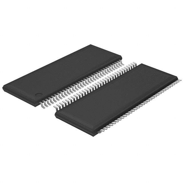
| 描述 | IC L-I PROTECTOR CIRCUIT 16SSOP电池管理 3-4-Cell Lithium-Ion Protection IC |
| 产品分类 | |
| 品牌 | Texas Instruments |
| 产品手册 | |
| 产品图片 |
|
| rohs | 符合RoHS无铅 / 符合限制有害物质指令(RoHS)规范要求 |
| 产品系列 | 电源管理 IC,电池管理,Texas Instruments UCC3957M-1- |
| 数据手册 | |
| 产品型号 | UCC3957M-1 |
| PCN过时产品 | |
| 产品目录页面 | |
| 产品种类 | 电池管理 |
| 供应商器件封装 | 16-SSOP |
| 其它名称 | 296-2234-5 |
| 功能 | 过压/欠压保护 |
| 包装 | 管件 |
| 商标 | Texas Instruments |
| 安装类型 | 表面贴装 |
| 安装风格 | SMD/SMT |
| 封装 | Tube |
| 封装/外壳 | 16-SSOP(0.154",3.90mm 宽) |
| 封装/箱体 | SSOP-16 |
| 工作温度 | -20°C ~ 70°C |
| 工作电源电压 | 5 V |
| 工厂包装数量 | 75 |
| 最大工作温度 | + 70 C |
| 最小工作温度 | - 20 C |
| 标准包装 | 75 |
| 电压-电源 | 5 V ~ 20 V |
| 电池化学 | 锂离子 |
| 电池类型 | Li-Ion |
| 系列 | UCC3957-1 |
| 输出电压 | 4.2 V |


- 商务部:美国ITC正式对集成电路等产品启动337调查
- 曝三星4nm工艺存在良率问题 高通将骁龙8 Gen1或转产台积电
- 太阳诱电将投资9.5亿元在常州建新厂生产MLCC 预计2023年完工
- 英特尔发布欧洲新工厂建设计划 深化IDM 2.0 战略
- 台积电先进制程称霸业界 有大客户加持明年业绩稳了
- 达到5530亿美元!SIA预计今年全球半导体销售额将创下新高
- 英特尔拟将自动驾驶子公司Mobileye上市 估值或超500亿美元
- 三星加码芯片和SET,合并消费电子和移动部门,撤换高东真等 CEO
- 三星电子宣布重大人事变动 还合并消费电子和移动部门
- 海关总署:前11个月进口集成电路产品价值2.52万亿元 增长14.8%


PDF Datasheet 数据手册内容提取
(cid:1)(cid:2)(cid:2)(cid:3)(cid:4)(cid:5)(cid:6)(cid:7)(cid:8)(cid:9) (cid:1)(cid:2)(cid:2)(cid:3)(cid:4)(cid:5)(cid:6)(cid:7)(cid:11)(cid:9) (cid:1)(cid:2)(cid:2)(cid:3)(cid:4)(cid:5)(cid:6)(cid:7)(cid:3)(cid:9) (cid:1)(cid:2)(cid:2)(cid:3)(cid:4)(cid:5)(cid:6)(cid:7)(cid:12) SLUS236B – JANUARY 1999 – REVISED SEPTEMBER 2002 (cid:13)(cid:14)(cid:15)(cid:16)(cid:16)(cid:7) (cid:17)(cid:15) (cid:18)(cid:17)(cid:1)(cid:15)(cid:7)(cid:2)(cid:16)(cid:19)(cid:19) (cid:19)(cid:20)(cid:13)(cid:14)(cid:20)(cid:1)(cid:21)(cid:7)(cid:20)(cid:17)(cid:22) (cid:23)(cid:15)(cid:17)(cid:13)(cid:16)(cid:2)(cid:13)(cid:17)(cid:15) (cid:2)(cid:20)(cid:15)(cid:2)(cid:1)(cid:20)(cid:13) FEATURES DESCRIPTION (cid:1) Three- or Four-Cell Operation The UCC3957 is a BiCMOS three- or four-cell (cid:1) Two-Tier Overcurrent Limiting lithium-ion battery pack protector designed to (cid:1) 30-µA Typical Supply-Current Consumption operate with external P-channel MOSFETs. Utilizing external P-channel MOSFETs provides (cid:1) 3.5-µA Typical Supply Current in Sleep Mode the benefits of no loss-of-system ground in an (cid:1) overdischarge state, and protects the IC as well as Smart Discharge Minimizes Losses in battery cells from damage during an overcharge Overcharge Mode state. An internal state machine runs continuously (cid:1) 6.5-V to 20-V VDD Supply Range to protect each lithium-ion cell from overcharge (cid:1) and overdischarge. A separate overcurrent- Highly Accurate Internal Voltage Reference protection block protects the battery pack from (cid:1) Externally Adjustable Delays in Overcurrent excessive discharge currents. Controller If any cell voltage exceeds the overvoltage (cid:1) Detection of Loss-of-Cell Sense Connections threshold, the appropriate external P-channel MOSFET is turned off, preventing further charge current. An external N-channel MOSFET is required to level shift to this high-side P-channel MOSFET. Discharge current can still flow through the second P-channel MOSFET. Likewise, if any M PACKAGE cell voltage falls below the undervoltage limit, the (TOP VIEW) second P-channel MOSFET is turned off and only charge current is allowed. Such a cell-voltage VDD 1 16 DVDD condition causes the chip to go into low-power CLCNT 2 15 AVDD sleep mode. Attempting to charge the battery pack wakes up the chip. A cell-count pin (CLCNT) WU 3 14 CDLY2 is provided to program the IC for three- or four-cell AN1 4 13 DCHG operations. AN2 5 12 CHG A two-tiered overcurrent controller and external AN3 6 11 AN4 current shunt protect the battery pack from AN4 7 10 CDLY1 excessive discharge currents. If the first BATLO 8 9 CHGEN overcurrent threshold level is exceeded, an internal timing circuit charges an external capacitor to provide a user programmable blanking time. If at the end of the blanking time the overcurrent condition still exists, the external discharge FET is turned off for a period 17 times longer than the first blanking period, and then the discharge FET is turned back on. If at any time a second higher overcurrent threshold is exceeded for more than a user programmable time, the discharge FET is turned off, and remains off for the same period as the first tier off time. This two tiered overcurrent-protection scheme allows for charging capacitive loads while retaining effective short-circuit protection. Please be aware that an important notice concerning availability, standard warranty, and use in critical applications of TexasInstruments semiconductor products and disclaimers thereto appears at the end of this data sheet. (cid:23)(cid:15)(cid:17)(cid:24)(cid:1)(cid:2)(cid:13)(cid:20)(cid:17)(cid:22) (cid:24)(cid:25)(cid:13)(cid:25) (cid:26)(cid:27)(cid:28)(cid:29)(cid:30)(cid:31) !(cid:26)(cid:29)(cid:27) (cid:26)" #$(cid:30)(cid:30)%(cid:27)! " (cid:29)(cid:28) &$’((cid:26)# !(cid:26)(cid:29)(cid:27) ) !%* Copyright 2002, Texas Instruments Incorporated (cid:23)(cid:30)(cid:29))$#!" #(cid:29)(cid:27)(cid:28)(cid:29)(cid:30)(cid:31) !(cid:29) "&%#(cid:26)(cid:28)(cid:26)# !(cid:26)(cid:29)(cid:27)" &%(cid:30) !+% !%(cid:30)(cid:31)" (cid:29)(cid:28) (cid:13)%, " (cid:20)(cid:27)"!(cid:30)$(cid:31)%(cid:27)!" "! (cid:27)) (cid:30)) - (cid:30)(cid:30) (cid:27)!.* (cid:23)(cid:30)(cid:29))$#!(cid:26)(cid:29)(cid:27) &(cid:30)(cid:29)#%""(cid:26)(cid:27)/ )(cid:29)%" (cid:27)(cid:29)! (cid:27)%#%"" (cid:30)(cid:26)(. (cid:26)(cid:27)#($)% !%"!(cid:26)(cid:27)/ (cid:29)(cid:28) (( & (cid:30) (cid:31)%!%(cid:30)"* www.ti.com 1
(cid:1)(cid:2)(cid:2)(cid:3)(cid:4)(cid:5)(cid:6)(cid:7)(cid:8)(cid:9) (cid:1)(cid:2)(cid:2)(cid:3)(cid:4)(cid:5)(cid:6)(cid:7)(cid:11)(cid:9) (cid:1)(cid:2)(cid:2)(cid:3)(cid:4)(cid:5)(cid:6)(cid:7)(cid:3)(cid:9) (cid:1)(cid:2)(cid:2)(cid:3)(cid:4)(cid:5)(cid:6)(cid:7)(cid:12) SLUS236B – JANUARY 1999 – REVISED SEPTEMBER 2002 block diagram VDD 1 16 DVDD CELL STATE VOLTAGE REFERENCE CLCNT 2 SELECT VOLTAGE MACHINE 15 AVDD SELECT AND WU 3 COMPARE 14 CDLY2 REF CLOCK AN1 4 13 DCHG UV S Q SLEEP AN2 5 12 CHG VDD R AN3 6 + 11 AN4 AN4 7 OVERCURRENT 10 CDLY1 CONTROLLER BATLO 8 9 CHGEN UDG–00129 absolute maximum ratings over operating free-air temperature range (unless otherwise noted)†‡ Supply voltage (VDD) . . . . . . . . . . . . . . . . . . . . . . . . . . . . . . . . . . . . . . . . . . . . . . . . . . . . . . . . . . . . . . . . . . . . . . 20 V Supply current . . . . . . . . . . . . . . . . . . . . . . . . . . . . . . . . . . . . . . . . . . . . . . . . . . . . . . . . . . . . . . . . . . . . . . . . . . . 25 mA Output current . . . . . . . . . . . . . . . . . . . . . . . . . . . . . . . . . . . . . . . . . . . . . . . . . . . . . . . . . . . . . . . . . . . . . . . . . . . 25 mA Input voltage: (WU) . . . . . . . . . . . . . . . . . . . . . . . . . . . . . . . . . . . . . . . . . . . . . . . . . . . . . . . . . . . . . . . . . . . . . . . 24 V (AN1, AN2, AN3). . . . . . . . . . . . . . . . . . . . . . . . . . . . . . . . . . . . . . . . . . . . . . . . . . . . . VAN4 – VDD (CLCNT, CHGEN) . . . . . . . . . . . . . . . . . . . . . . . . . . . . . . . . . . . . . . . . . . . . . . . . . . . . . . . . . . . . 15 V Input voltage range (BATLO) . . . . . . . . . . . . . . . . . . . . . . . . . . . . . . . . . . . . . . . . . . . . . . . . . . . . . . . . –0.3 V to 2.5 V Storage temperature range, T . . . . . . . . . . . . . . . . . . . . . . . . . . . . . . . . . . . . . . . . . . . . . . . . . . . . –65°C to 150°C stg Operating virtual junction temperature range, T . . . . . . . . . . . . . . . . . . . . . . . . . . . . . . . . . . . . . . –55°C to 150°C J Lead temperature (soldering, 10 seconds) . . . . . . . . . . . . . . . . . . . . . . . . . . . . . . . . . . . . . . . . . . . . . . . . . . . 300°C †Stresses beyond those listed under “absolute maximum ratings” may cause permanent damage to the device. These are stress ratings only, and functional operation of the device at these or any other conditions beyond those indicated under “recommended operating conditions” is not implied. Exposure to absolute-maximum-rated conditions for extended periods may affect device reliability. ‡Unless otherwise indicated, voltages are reference to ground and currents are positive into and negative out of the specified terminals. Consult Packaging Information section of the Portable Products Databook (TI Literature No. SLUD001) for thermal limitations and considerations of packages. All voltages are referenced to the AN4 terminal. AVAILABLE OPTIONS PACKAGED DEVICES† SSOP (M) TTA NORMAL TO OVERCHARGE VOLTAGE (V) 4.20 4.25 4.30 4.35 –20°C to 70°C UCC3957M–1 UCC3957M–2 UCC3957M–3 UCC3957M–4 †The M package is available taped and reeled. Add TR suffix to device type (e.g. UCC3957M–1TR) to order quantities of 2500 devices per reel. 2 www.ti.com
(cid:1)(cid:2)(cid:2)(cid:3)(cid:4)(cid:5)(cid:6)(cid:7)(cid:8)(cid:9) (cid:1)(cid:2)(cid:2)(cid:3)(cid:4)(cid:5)(cid:6)(cid:7)(cid:11)(cid:9) (cid:1)(cid:2)(cid:2)(cid:3)(cid:4)(cid:5)(cid:6)(cid:7)(cid:3)(cid:9) (cid:1)(cid:2)(cid:2)(cid:3)(cid:4)(cid:5)(cid:6)(cid:7)(cid:12) SLUS236B – JANUARY 1999 – REVISED SEPTEMBER 2002 electrical characteristics over recommended operating free-air temperature range, VDD = 16 V, –20(cid:2)C < T < 70(cid:2)C, T = T . (unless otherwise noted) A A J supply PARAMETER TEST CONDITIONS MIN TYP MAX UNIT VDDmin Minimum VDD 5.0 5.5 V IDD Supply current 30 40 µA ISL Sleep-mode supply current VDD = 10.4 V 3.5 7.5 µA VIN Input voltage for WU See Note 2 20 V output PARAMETER TEST CONDITIONS MIN TYP MAX UNIT Driving-logic low, VO = 1 V 40 70 100 µA IIDCHG DDCCHHGG oouttpputt ccurrrreenntt Driving-logic high, VO = (VDD – 1) –13 –3 mA Driving-logic low, VO = 1 V 40 70 100 µA IICHG CCHHGG oouuppuutt ccuurrrreenntt Driving-logic high, VO = (VDD – 1V) –15 –3 mA state transitions PARAMETER TEST CONDITIONS MIN TYP MAX UNIT VOV Normal to overcharge voltage See Note 1 4.15 4.20 4.25 V UUCCCC33995577–11 VOVR Overcharge to normal voltage 3.95 4.00 4.05 V VOV Normal to overcharge voltage See Note 1 4.20 4.25 4.30 V UUCCCC33995577–22 VOVR Overcharge to normal voltage 4.00 4.05 4.10 V VOV Normal to overcharge voltage See Note 1 4.25 4.30 4.35 V UUCCCC33995577–33 VOVR Overcharge to normal voltage 4.05 4.10 4.15 V VOV Normal to overcharge voltage See Note 1 4.30 4.35 4.40 V UUCCCC33995577–44 VOVR Overcharge to normal voltage 4.10 4.15 4.20 V VUV Undercharge to normal voltage See Note 1 2.5 2.6 2.7 V VUVR Normal to undercharge voltage 2.2 2.3 2.4 V tdOV Overvoltage to CHG delay 8 17 23 ms tdUV Undervoltage to DCHG Delay 8 17 23 ms tS Cell sample rate 4 8.5 11.5 ms VSM Smart discharge threshold BATLO voltage 4 15 25 mV VWU Wakeup input threshold With respect to VDD 50 230 750 mV VCE Charge-enable input threshold 0.8 1.3 2.6 V short-circuit protection PARAMETER TEST CONDITIONS MIN TYP MAX UNIT VCL1 First-tier threshold level VBATLO 120 150 190 mV VCL2 Second-tier threshold level VBATLO 275 375 450 mV tB1 First-tier blanking time CDLY1 = 0.1 µF 30 50 70 ms tRST Restart time CDLY1 = 0.1 µF 300 500 700 ms tB2 Second-tier blanking time CDLY2 = 10 pF 100 400 600 µs NOTE 1: Other overvoltage or undervoltage thresholds are available. Please consult the factory. 2: Refer to Figure 6, for WU leakage characteristics. www.ti.com 3
(cid:1)(cid:2)(cid:2)(cid:3)(cid:4)(cid:5)(cid:6)(cid:7)(cid:8)(cid:9) (cid:1)(cid:2)(cid:2)(cid:3)(cid:4)(cid:5)(cid:6)(cid:7)(cid:11)(cid:9) (cid:1)(cid:2)(cid:2)(cid:3)(cid:4)(cid:5)(cid:6)(cid:7)(cid:3)(cid:9) (cid:1)(cid:2)(cid:2)(cid:3)(cid:4)(cid:5)(cid:6)(cid:7)(cid:12) SLUS236B – JANUARY 1999 – REVISED SEPTEMBER 2002 Terminal Functions TERMINAL II//OO DDEESSCCRRIIPPTTIIOONN NAME NO. AN1 4 I Connects to the negative terminal of the top battery cell and the positive terminal of the second battery cell. AN2 5 I Connects to the bottom terminal of the second battery cell and the top terminal of the third battery cell. AN3 6 Connects to the bottom terminal of the third battery cell and the top terminal of the fourth battery cell in a four I cell stack. In a three cell pack it connects to the bottom terminal of the third battery and to AN4. AN4 7 I Connects to the bottom terminal of the battery stack and the top of the current sense resistor. AVDD 15 Internal analog supply bypass cap pin. Connect a 0.1-µF capacitor between this pin and AN4. This pin is O nominally 7.3 V. BATLO 8 I Connects to the bottom of the current sense resistor and the negative terminal of the battery pack. CHGEN 9 The charge enable input for the protection IC. This point must be driven high to DVDD or AVDD to allow I charging of the battery pack. This pin has a very weak pulldown. CDLY1 10 Delay control pin for the short-circuit protection feature. A capacitor connected between this point and AN4 O determines the time delay from when an overcurrent situation is detected to when the FET is turned off. This capacitor also controls the hiccup mode timeout period. CDLY2 14 An external cap can be tied between this pin and AN4 to extend the blanking time on the second current limit O tier. CLCNT 2 This pin programs the IC for three or four cell operation. Tying this pin low (to AN4) sets four cell operation, I while tying it high (to DVDD or AVDD) sets three cell operation. This pin is internally pulled low, so open cir- cuit conditions always result in four-cell mode. DCHG 13 This pin is used to prevent overdischarge. If the state machine indicates that any cell is undervoltage, this pin O is driven high with respect to chip substrate so that the external P-channel MOSFET prevents further dis- charge. If all cell voltages are above the minimum threshold, this pin is driven low. CHG 12 This pin is used to control an external N-channel MOSFET, which in turn drives a P-channel MOSFET. If at O least one cell voltage is over the overvoltage threshold, this pin is driven low with respect to AN4. If all cell voltages are below this threshold, this pin is driven high. DVDD 16 Internal digital supply bypass capacitor pin. Connect a 0.1-µF capacitor between this pin and AN4. This pin is O nominally 7.3V. VDD 1 I Supply voltage to the IC. Connect this point to the top of the lithium-ion battery stack. WU 3 This pin is used to provide a wakeup signal to the IC during sleep mode. Connect this pin to the drain of the I N-channel level shift MOSFET. 4 www.ti.com
(cid:1)(cid:2)(cid:2)(cid:3)(cid:4)(cid:5)(cid:6)(cid:7)(cid:8)(cid:9) (cid:1)(cid:2)(cid:2)(cid:3)(cid:4)(cid:5)(cid:6)(cid:7)(cid:11)(cid:9) (cid:1)(cid:2)(cid:2)(cid:3)(cid:4)(cid:5)(cid:6)(cid:7)(cid:3)(cid:9) (cid:1)(cid:2)(cid:2)(cid:3)(cid:4)(cid:5)(cid:6)(cid:7)(cid:12) SLUS236B – JANUARY 1999 – REVISED SEPTEMBER 2002 APPLICATION INFORMATION overview The UCC3957 provides complete protection against overdischarge, overcharge and overcurrent for a three- or four-cell lithium-ion battery pack. It uses a flying capacitor technique to sample the voltage across each battery cell and compare it to a precision reference. If any cell is in overvoltage or undervoltage, the internal-state machine takes the appropriate action to prevent further charge or discharge. High-side P-channel MOSFETs are used to independently control charge and discharge current. Figure 1 shows a three-cell lithium-ion protector application diagram with the optional charge-enable switch. In this application, the diode D1 protects the MOSFET Q2 from inductive kick at turn-off. R1 PACK (+) 1 MΩ Q1 Q3 IFR7416 2N7002 D1 CHARGE 1 A, 50 V Q2 IFR7416 DISCHARGE C1 0.1 µF 1 VDD DVDD 16 LI–ION C2 BATTERY C5 0.1 µF STACK 4.7 µF 2 CLCNT AVDD 15 C3 25 V OPTIONAL 3 WU CDLY2 14 + 4 AN1 DCHG 13 + 5 AN2 CHG 12 + 6 AN3 AN4 11 C4 0.022 µF RSENSE 7 AN4 CDLY1 10 0.025 Ω PACK (–) 8 BATLO CHGEN 9 S1 CLOSE TO ENABLE CHARGING UDG–98016 Figure 1. Three-Cell Lithium-Ion Protector Application Diagram www.ti.com 5
(cid:1)(cid:2)(cid:2)(cid:3)(cid:4)(cid:5)(cid:6)(cid:7)(cid:8)(cid:9) (cid:1)(cid:2)(cid:2)(cid:3)(cid:4)(cid:5)(cid:6)(cid:7)(cid:11)(cid:9) (cid:1)(cid:2)(cid:2)(cid:3)(cid:4)(cid:5)(cid:6)(cid:7)(cid:3)(cid:9) (cid:1)(cid:2)(cid:2)(cid:3)(cid:4)(cid:5)(cid:6)(cid:7)(cid:12) SLUS236B – JANUARY 1999 – REVISED SEPTEMBER 2002 APPLICATION INFORMATION overview (continued) Figure 2 shows a four-cell protector with optional components to protect the charge FET from excessive gate-to-source transients. In this application, the Zener diode VR1 and the resistor R2 are optional. They protect the MOSFET Q1 from excessive open-circuit charger voltage. Diode D1 protects MOSFET Q2 from inductive kick during turn-off. VR1 18 V PACK (+) R1 1 MΩ R2 Q1 10 kΩ D1 IFR7416 1 A, 50 V CHARGE Q3 2N7002 Q2 IFR7416 DISCHARGE C5 4.7 µF C1 25 V 0.1 µF 1 VDD DVDD 16 C2 LI–ION 0.1 µF 2 CLCNT AVDD 15 BATTERY C3 STACK OPTIONAL 3 WU CDLY2 14 + 4 AN1 DCHG 13 + 5 AN2 CHG 12 + 6 AN3 AN4 11 + C4 0.022 µF 7 AN4 CDLY1 10 RSENSE 8 BATLO CHGEN 9 PACK (–) 0.025 Ω UDG–98017 Figure 2. Four-Cell Lithium-Ion Protector Application Diagram connecting the cell stack When connecting the cell stack to the circuit, it is important to do so in the proper order. First, the bottom of the stack should be connected to AN4 . Next, the top of the stack should be connected to VDD. The cell taps can then be connected to AN1, AN2, and AN3 in any order. choosing three or four cells For three-cell packs, the cell-count pin (CLCNT) should be connected to the DVDD pin, and the AN3 pin should be tied to the AN4 pin. For four-cell applications, the CLCNT pin should be grounded (to AN4) and the AN3 pin is connected to the positive terminal of the bottom cell in the stack. 6 www.ti.com
(cid:1)(cid:2)(cid:2)(cid:3)(cid:4)(cid:5)(cid:6)(cid:7)(cid:8)(cid:9) (cid:1)(cid:2)(cid:2)(cid:3)(cid:4)(cid:5)(cid:6)(cid:7)(cid:11)(cid:9) (cid:1)(cid:2)(cid:2)(cid:3)(cid:4)(cid:5)(cid:6)(cid:7)(cid:3)(cid:9) (cid:1)(cid:2)(cid:2)(cid:3)(cid:4)(cid:5)(cid:6)(cid:7)(cid:12) SLUS236B – JANUARY 1999 – REVISED SEPTEMBER 2002 APPLICATION INFORMATION undervoltage protection When any cell is found to be overdischarged (below the normal-to-undercharge threshold), the state machine turns off both high-side FETs and enters the sleep mode, where current consumption drops to about 3.5 µA. It remains in sleep mode until the application of a charger is sensed by the wakeup pin (WU) being raised above VDD. charging Once a charger has been applied, the charge FET is turned on as long as the charge-enable input pin (CHGEN) is pulled up to the DVDD pin. If the CHGEN input is left open (or connected to AN4), the charge FET remains off. During charge, the charge and discharge FETs cycle on and off while the device is in the sleep state (undercharge mode), until the cell voltages are all above the undercharge-to-normal threshold. Once the cell voltages are above this threshold, the device enters the normal state and the FETs remain on continuously. While the device is charging and in undercharge mode, there is an approximate on time of 8 ms corresponding to one sampling period, with a very short off time corresponding to undercharge-voltage detect and sleep-mode; once WU is pulled back up to PACK(+), wake-up detect again occurs, and a new sampling period/charge cycle is initiated. open wire protection The UCC3957 provides protection against broken-cell sense connections within the pack. If the sense connection to one of the cells (pins AN1, AN2, or AN3) should become disconnected, weak internal-current sources make the cells that are connected to that wire appear to be in overcharge and charging of the pack is prevented. overvoltage protection and the smart discharge feature If any cell is charged to a voltage exceeding the normal-to-overcharge threshold, the charge FET is turned off, preventing further charge current. Hysteresis keeps the charge FET off until the cell voltages have dropped below the overcharge-to-normal threshold. In most protector designs, the charge FET is held off completely within this voltage band. During this time, discharge current must be conducted through the body diode of the charge FET. This forward voltage drop can be as high as 1 V, causing significant power dissipation in the charge FET and wasting precious battery power. The UCC3957 has a unique smart discharge feature that allows the charge FET to return to on mode (for discharge only) while still in the overcharge hysteresis band. This greatly reduces power dissipation in the charge FET. This is accomplished by sensing the voltage drop across the current-sense resistor. If this drop exceeds 15 mV (corresponding to 0.6 A of discharge current using a .025 Ω sense resistor), the charge FET is turned back on. This threshold assures that only discharge current is conducted. In an example using a 20-mW FET with a 1-V body diode drop and a 1-A load, the power dissipation in Q1 would be reduced from 1 W to 0.02 W. NOTE: A similar technique is not used during charge (when the discharge MOSFET is off due to cells being in undervoltage) because the charge current should be low while the cells are in undervoltage. www.ti.com 7
(cid:1)(cid:2)(cid:2)(cid:3)(cid:4)(cid:5)(cid:6)(cid:7)(cid:8)(cid:9) (cid:1)(cid:2)(cid:2)(cid:3)(cid:4)(cid:5)(cid:6)(cid:7)(cid:11)(cid:9) (cid:1)(cid:2)(cid:2)(cid:3)(cid:4)(cid:5)(cid:6)(cid:7)(cid:3)(cid:9) (cid:1)(cid:2)(cid:2)(cid:3)(cid:4)(cid:5)(cid:6)(cid:7)(cid:12) SLUS236B – JANUARY 1999 – REVISED SEPTEMBER 2002 APPLICATION INFORMATION protection against a runaway charger The use of a small N-channel level shifter (Q3 in the application diagrams) allows the IC to interface with the high-side charge FET (Q1), even in the presence of a runaway charger. Only the drain-source voltage rating of the charge FET limits the charge voltage that the protection circuit can withstand. The wakeup (WU) pin is designed to handle input voltages greater than VDD, as long as the current is limited. In the examples shown, the charge FET’s gate-source resistor (R1) provides this current limiting. Note that in Figure 2, a resistor and zener (R2 and VR1) have been added to protect Q1 against any possibility of a voltage transient exceeding its maximum gate-source rating. overcurrent protection The UCC3957 protects the battery pack from an overload or a hard short circuit using a two-tier overcurrent protection scheme. The overcurrent protection is designed to go into a hiccup mode when the voltage drop across an external-sense resistor (connected to the AN4 and BATLO pins) exceeds a certain threshold. In this mode, the discharge FET is periodically turned off and on until the fault is removed. Once the fault is removed, normal operation is automatically resumed. To facilitate charging large capacitive loads, there are two overcurrent threshold voltages, each with its own user-programmable time delay. This two-tier approach provides fast response to short circuits, while enabling the battery pack to provide short-duration surge currents. It also facilitates the charging of large filter caps without causing nuisance overcurrent trips. The first-tier threshold is 150 mV nominal, corresponding to 6 A using a .025-Ω sense resistor as shown in the examples of Figure 1 and Figure 2. If the pack-discharge current exceeds this amount for a period of time, determined by the capacitor on the CDLY1 pin, it then enters the hiccup mode. The first-tier hiccup duty cycle is fixed at approximately 6%, minimizing power dissipation in the event of a sustained overload. The absolute on and off times of the discharge FET (Q2) are controlled by the CDLY1 capacitor. A curve relating the delay (on time) to this capacitor value is shown in Figure 4. The off time is approximately 17 times longer than the on time. The second-tier overcurrent threshold is nominally 375 mV, corresponding to 15 A using a .025-Ω sense resistor. If the pack current exceeds this value for a period of time, determined by the capacitor on the CDLY2 pin, it then enters the hiccup-mode with a much lower duty cycle, typically less than 1%. The relationship of this time delay (on time) to the CDLY2 capacitor value is shown in the curve of Figure 5. The off time during this hiccup mode is still determined by the CDLY1 capacitor, as previously described. This technique greatly reduces the stress and power dissipation in the FETs during short-circuit conditions. In the examples shown in Figure 1 and Figure 2 (with CDLY1 = .022 µF), the first-tier overcurrent on time is approximately 10 msec, while the off time is approximately 170 msec, resulting in a 5.9% duty cycle for currents over 6 A (but less than 15 A). If no CDLY2 capacitor is used, the second-tier on time is less than 200 µsec (assuming no stray capacitance), resulting in a duty cycle of about 0.1% for currents over 15 A. If CDLY2 = 22pF, the typical on time for currents exceeding 15 A is approximately 800 µsec, resulting in a duty cycle of 0.5%. 8 www.ti.com
(cid:1)(cid:2)(cid:2)(cid:3)(cid:4)(cid:5)(cid:6)(cid:7)(cid:8)(cid:9) (cid:1)(cid:2)(cid:2)(cid:3)(cid:4)(cid:5)(cid:6)(cid:7)(cid:11)(cid:9) (cid:1)(cid:2)(cid:2)(cid:3)(cid:4)(cid:5)(cid:6)(cid:7)(cid:3)(cid:9) (cid:1)(cid:2)(cid:2)(cid:3)(cid:4)(cid:5)(cid:6)(cid:7)(cid:12) SLUS236B – JANUARY 1999 – REVISED SEPTEMBER 2002 APPLICATION INFORMATION protecting against inductive kick at turn-off In the case of a short circuit, the di/dt that occurs when the discharge FET is turned off can result in a significant voltage undershoot at the pack output due to stray inductance. This undershoot can potentially exceed the breakdown voltage rating of the discharge FET. A clamp diode (D1 in Figure 1, Figure 2, and Figure 3), or a capacitor across the pack output, protects against this possibility. A diode also provides protection from a reverse-polarity charger. During turn-off, a voltage overshoot can occur at the top of the cell stack, due to wiring inductance and the cells’ internal equivalent series inductance (ESL). During very high di/dt conditions, such as occurs when turning off in response to a short circuit, this voltage overshoot can be significant and potentially damage the IC or the discharge FET (Q2). For this reason, it is strongly recommended that a capacitor (C5) be placed across the cell stack, from VDD to AN4, and that stray inductance be minimized in the battery-current path. Additional methods to reduce di/dt across the cell stack are discussed in the following section. controlling discharge FET turn-on and turn-off times Slew-rate limiting the pack output voltage at turn-on greatly reduces the surge current into large capacitive loads. This allows the designer to select shorter overcurrent-delay times, minimizing the stress on Q1 and Q2 in the event of a shorted pack output. A simple method of implementing slew-rate limiting is shown in Figure 3. It consists of an RC network (R3 and C6) between gate and drain of the discharge FET (Q2) to control its turn-on time. This circuit relies on the relatively high-sink impedance (about 20 kΩ) of the UCC3957’s DCHG output. The values shown for R3 and C6 provide a pack output voltage rise time of about 4.5 ms when the discharge FET (Q2) is turned on. Note that the addition of R3 and C6 has made it possible to eliminate the CDLY2 capacitor, for the quickest response to a true short circuit. While this circuit does not prevent a large surge current when inserting a live battery pack into a highly-capacitive load, it does allow it to restart (after one hiccup cycle) if this initial surge-current trips the overcurrent protection. Increasing the turn-off time of the discharge FET (Q2) reduces the inductive kick that results during turn-off after an overcurrent condition. This is accomplished by adding a resistor (R4) in series with the DCHG output. This reduction of di/dt at turn-off minimizes the need for a capacitor across the battery stack. It is recommended that this resistor value not exceed a few hundred Ohms, in which case the ability to turn off quickly enough into a short may be compromised. Due to the relatively low-charge currents (typically a few Amperes max), controlling the turn-on and turn-off times of the charge FET is not beneficial. In fact, the turn-off time of the charge FET is slow due to the large value of R1, the gate-to-source resistor. www.ti.com 9
(cid:1)(cid:2)(cid:2)(cid:3)(cid:4)(cid:5)(cid:6)(cid:7)(cid:8)(cid:9) (cid:1)(cid:2)(cid:2)(cid:3)(cid:4)(cid:5)(cid:6)(cid:7)(cid:11)(cid:9) (cid:1)(cid:2)(cid:2)(cid:3)(cid:4)(cid:5)(cid:6)(cid:7)(cid:3)(cid:9) (cid:1)(cid:2)(cid:2)(cid:3)(cid:4)(cid:5)(cid:6)(cid:7)(cid:12) SLUS236B – JANUARY 1999 – REVISED SEPTEMBER 2002 APPLICATION INFORMATION controlling discharge FET turn-on and turn-off times Figure 3 shows a four-cell protector with slew-rate limiting the discharge FET. In this application, VR1 and R2 are optional, They protect Q1 from excessive open-circuit charger voltage. R3 and C6 are chosen based on capacitive load that must be driven. R4 minimizes inductive kick at turn-off. VR1 18 V PACK (+) R1 1 MΩ R2 Q1 10 kΩ D1 IFR7416 1 A, 50 V CHARGE R3 1 kΩ C6 Q3 0.22 µF 2N7002 R4 Q2 100 Ω IFR7416 DISCHARGE C5 4.7 µF C1 25 V 0.1 µF 1 VDD DVDD 16 C2 LI–ION 0.1 µF 2 CLCNT AVDD 15 BATTERY C3 STACK OPTIONAL 3 WU CDLY2 14 + 4 AN1 DCHG 13 + 5 AN2 CHG 12 + 6 AN3 AN4 11 C4 + 0.022 µF 7 AN4 CDLY1 10 RSENSE 8 BATLO CHGEN 9 PACK (–) 0.025 Ω UDG–98018 Figure 3. Four-Cell Lithium-Ion Protector Application Diagram 10 www.ti.com
(cid:1)(cid:2)(cid:2)(cid:3)(cid:4)(cid:5)(cid:6)(cid:7)(cid:8)(cid:9) (cid:1)(cid:2)(cid:2)(cid:3)(cid:4)(cid:5)(cid:6)(cid:7)(cid:11)(cid:9) (cid:1)(cid:2)(cid:2)(cid:3)(cid:4)(cid:5)(cid:6)(cid:7)(cid:3)(cid:9) (cid:1)(cid:2)(cid:2)(cid:3)(cid:4)(cid:5)(cid:6)(cid:7)(cid:12) SLUS236B – JANUARY 1999 – REVISED SEPTEMBER 2002 TYPICAL CHARACTERISTICS TYPICAL TIER-ONE OVERCURRENT DELAY TIME TYPICAL TIER-TWO OVERCURRENT DELAY TIME vs vs DELAY CAPACITANCE DELAY CAPACITANCE 1000 1400 1200 100 s 1000 me – m Off-time µme – s 800 Delay Ti 10 Delay Ti 600 – D – D t t 400 1 Delay 200 0.1 0 0.001 0.01 0.1 0 10 20 30 40 CCDLY1 – Delay Capacitance – µF CCDLY2 – Delay Capacitance – pF Figure 4 Figure 5 WU LEAKAGE CURRENT vs INPUT VOLTAGE 70 Maximum A µ 60 – nt e rr 50 u C e g Typical a k 40 a e L U W – 30 U Minimum W I 20 10 0 14 16 18 20 22 24 26 VWU – Wake-Up Input Voltage – V Figure 6 www.ti.com 11
PACKAGE OPTION ADDENDUM www.ti.com 30-Jul-2009 PACKAGING INFORMATION OrderableDevice Status(1) Package Package Pins Package EcoPlan(2) Lead/BallFinish MSLPeakTemp(3) Type Drawing Qty UCC3957M-1 ACTIVE SSOP/ DBQ 16 75 Green(RoHS& CUNIPDAU Level-2-260C-1YEAR QSOP noSb/Br) UCC3957M-1G4 ACTIVE SSOP/ DBQ 16 75 Green(RoHS& CUNIPDAU Level-2-260C-1YEAR QSOP noSb/Br) UCC3957M-2 ACTIVE SSOP/ DBQ 16 75 Green(RoHS& CUNIPDAU Level-2-260C-1YEAR QSOP noSb/Br) UCC3957M-2G4 ACTIVE SSOP/ DBQ 16 75 Green(RoHS& CUNIPDAU Level-2-260C-1YEAR QSOP noSb/Br) UCC3957M-3 ACTIVE SSOP/ DBQ 16 75 Green(RoHS& CUNIPDAU Level-2-260C-1YEAR QSOP noSb/Br) UCC3957M-3G4 ACTIVE SSOP/ DBQ 16 75 Green(RoHS& CUNIPDAU Level-2-260C-1YEAR QSOP noSb/Br) UCC3957M-4 ACTIVE SSOP/ DBQ 16 75 Green(RoHS& CUNIPDAU Level-2-260C-1YEAR QSOP noSb/Br) UCC3957M-4G4 ACTIVE SSOP/ DBQ 16 75 Green(RoHS& CUNIPDAU Level-2-260C-1YEAR QSOP noSb/Br) UCC3957MTR-1 ACTIVE SSOP/ DBQ 16 TBD CallTI CallTI QSOP UCC3957MTR-1G4 ACTIVE SSOP/ DBQ 16 TBD CallTI CallTI QSOP UCC3957MTR-2 ACTIVE SSOP/ DBQ 16 2500 Green(RoHS& CUNIPDAU Level-2-260C-1YEAR QSOP noSb/Br) UCC3957MTR-2G4 ACTIVE SSOP/ DBQ 16 2500 Green(RoHS& CUNIPDAU Level-2-260C-1YEAR QSOP noSb/Br) UCC3957MTR-3 ACTIVE SSOP/ DBQ 16 2500 Green(RoHS& CUNIPDAU Level-2-260C-1YEAR QSOP noSb/Br) UCC3957MTR-3G4 ACTIVE SSOP/ DBQ 16 2500 Green(RoHS& CUNIPDAU Level-2-260C-1YEAR QSOP noSb/Br) UCC3957MTR-4 ACTIVE SSOP/ DBQ 16 2500 Green(RoHS& CUNIPDAU Level-2-260C-1YEAR QSOP noSb/Br) UCC3957MTR-4G4 ACTIVE SSOP/ DBQ 16 2500 Green(RoHS& CUNIPDAU Level-2-260C-1YEAR QSOP noSb/Br) (1)Themarketingstatusvaluesaredefinedasfollows: ACTIVE:Productdevicerecommendedfornewdesigns. LIFEBUY:TIhasannouncedthatthedevicewillbediscontinued,andalifetime-buyperiodisineffect. NRND:Notrecommendedfornewdesigns.Deviceisinproductiontosupportexistingcustomers,butTIdoesnotrecommendusingthispartin anewdesign. PREVIEW:Devicehasbeenannouncedbutisnotinproduction.Samplesmayormaynotbeavailable. OBSOLETE:TIhasdiscontinuedtheproductionofthedevice. (2)EcoPlan-Theplannedeco-friendlyclassification:Pb-Free(RoHS),Pb-Free(RoHSExempt),orGreen(RoHS&noSb/Br)-pleasecheck http://www.ti.com/productcontentforthelatestavailabilityinformationandadditionalproductcontentdetails. TBD:ThePb-Free/Greenconversionplanhasnotbeendefined. Pb-Free(RoHS):TI'sterms"Lead-Free"or"Pb-Free"meansemiconductorproductsthatarecompatiblewiththecurrentRoHSrequirements forall6substances,includingtherequirementthatleadnotexceed0.1%byweightinhomogeneousmaterials.Wheredesignedtobesoldered athightemperatures,TIPb-Freeproductsaresuitableforuseinspecifiedlead-freeprocesses. Pb-Free(RoHSExempt):ThiscomponenthasaRoHSexemptionforeither1)lead-basedflip-chipsolderbumpsusedbetweenthedieand package, or 2) lead-based die adhesive used between the die and leadframe. The component is otherwise considered Pb-Free (RoHS compatible)asdefinedabove. Green(RoHS&noSb/Br):TIdefines"Green"tomeanPb-Free(RoHScompatible),andfreeofBromine(Br)andAntimony(Sb)basedflame retardants(BrorSbdonotexceed0.1%byweightinhomogeneousmaterial) Addendum-Page1
PACKAGE OPTION ADDENDUM www.ti.com 30-Jul-2009 (3) MSL, Peak Temp. -- The Moisture Sensitivity Level rating according to the JEDEC industry standard classifications, and peak solder temperature. Important Information and Disclaimer:The information provided on this page represents TI's knowledge and belief as of the date that it is provided. TI bases its knowledge and belief on information provided by third parties, and makes no representation or warranty as to the accuracy of such information. Efforts are underway to better integrate information from third parties. TI has taken and continues to take reasonable steps to provide representative and accurate information but may not have conducted destructive testing or chemical analysis on incomingmaterialsandchemicals.TIandTIsuppliersconsidercertaininformationtobeproprietary,andthusCASnumbersandotherlimited informationmaynotbeavailableforrelease. InnoeventshallTI'sliabilityarisingoutofsuchinformationexceedthetotalpurchasepriceoftheTIpart(s)atissueinthisdocumentsoldbyTI toCustomeronanannualbasis. Addendum-Page2
PACKAGE MATERIALS INFORMATION www.ti.com 29-Jul-2009 TAPE AND REEL INFORMATION *Alldimensionsarenominal Device Package Package Pins SPQ Reel Reel A0 B0 K0 P1 W Pin1 Type Drawing Diameter Width (mm) (mm) (mm) (mm) (mm) Quadrant (mm) W1(mm) UCC3957MTR-2 SSOP/ DBQ 16 2500 330.0 12.4 6.4 5.2 2.1 8.0 12.0 Q1 QSOP UCC3957MTR-3 SSOP/ DBQ 16 2500 330.0 12.4 6.4 5.2 2.1 8.0 12.0 Q1 QSOP UCC3957MTR-4 SSOP/ DBQ 16 2500 330.0 12.4 6.4 5.2 2.1 8.0 12.0 Q1 QSOP PackMaterials-Page1
PACKAGE MATERIALS INFORMATION www.ti.com 29-Jul-2009 *Alldimensionsarenominal Device PackageType PackageDrawing Pins SPQ Length(mm) Width(mm) Height(mm) UCC3957MTR-2 SSOP/QSOP DBQ 16 2500 346.0 346.0 29.0 UCC3957MTR-3 SSOP/QSOP DBQ 16 2500 346.0 346.0 29.0 UCC3957MTR-4 SSOP/QSOP DBQ 16 2500 346.0 346.0 29.0 PackMaterials-Page2
None
None
IMPORTANTNOTICE TexasInstrumentsIncorporatedanditssubsidiaries(TI)reservetherighttomakecorrections,modifications,enhancements,improvements, andotherchangestoitsproductsandservicesatanytimeandtodiscontinueanyproductorservicewithoutnotice.Customersshould obtainthelatestrelevantinformationbeforeplacingordersandshouldverifythatsuchinformationiscurrentandcomplete.Allproductsare soldsubjecttoTI’stermsandconditionsofsalesuppliedatthetimeoforderacknowledgment. TIwarrantsperformanceofitshardwareproductstothespecificationsapplicableatthetimeofsaleinaccordancewithTI’sstandard warranty.TestingandotherqualitycontroltechniquesareusedtotheextentTIdeemsnecessarytosupportthiswarranty.Exceptwhere mandatedbygovernmentrequirements,testingofallparametersofeachproductisnotnecessarilyperformed. TIassumesnoliabilityforapplicationsassistanceorcustomerproductdesign.Customersareresponsiblefortheirproductsand applicationsusingTIcomponents.Tominimizetherisksassociatedwithcustomerproductsandapplications,customersshouldprovide adequatedesignandoperatingsafeguards. TIdoesnotwarrantorrepresentthatanylicense,eitherexpressorimplied,isgrantedunderanyTIpatentright,copyright,maskworkright, orotherTIintellectualpropertyrightrelatingtoanycombination,machine,orprocessinwhichTIproductsorservicesareused.Information publishedbyTIregardingthird-partyproductsorservicesdoesnotconstitutealicensefromTItousesuchproductsorservicesora warrantyorendorsementthereof.Useofsuchinformationmayrequirealicensefromathirdpartyunderthepatentsorotherintellectual propertyofthethirdparty,oralicensefromTIunderthepatentsorotherintellectualpropertyofTI. ReproductionofTIinformationinTIdatabooksordatasheetsispermissibleonlyifreproductioniswithoutalterationandisaccompanied byallassociatedwarranties,conditions,limitations,andnotices.Reproductionofthisinformationwithalterationisanunfairanddeceptive businesspractice.TIisnotresponsibleorliableforsuchaltereddocumentation.Informationofthirdpartiesmaybesubjecttoadditional restrictions. ResaleofTIproductsorserviceswithstatementsdifferentfromorbeyondtheparametersstatedbyTIforthatproductorservicevoidsall expressandanyimpliedwarrantiesfortheassociatedTIproductorserviceandisanunfairanddeceptivebusinesspractice.TIisnot responsibleorliableforanysuchstatements. TIproductsarenotauthorizedforuseinsafety-criticalapplications(suchaslifesupport)whereafailureoftheTIproductwouldreasonably beexpectedtocauseseverepersonalinjuryordeath,unlessofficersofthepartieshaveexecutedanagreementspecificallygoverning suchuse.Buyersrepresentthattheyhaveallnecessaryexpertiseinthesafetyandregulatoryramificationsoftheirapplications,and acknowledgeandagreethattheyaresolelyresponsibleforalllegal,regulatoryandsafety-relatedrequirementsconcerningtheirproducts andanyuseofTIproductsinsuchsafety-criticalapplications,notwithstandinganyapplications-relatedinformationorsupportthatmaybe providedbyTI.Further,BuyersmustfullyindemnifyTIanditsrepresentativesagainstanydamagesarisingoutoftheuseofTIproductsin suchsafety-criticalapplications. TIproductsareneitherdesignednorintendedforuseinmilitary/aerospaceapplicationsorenvironmentsunlesstheTIproductsare specificallydesignatedbyTIasmilitary-gradeor"enhancedplastic."OnlyproductsdesignatedbyTIasmilitary-grademeetmilitary specifications.BuyersacknowledgeandagreethatanysuchuseofTIproductswhichTIhasnotdesignatedasmilitary-gradeissolelyat theBuyer'srisk,andthattheyaresolelyresponsibleforcompliancewithalllegalandregulatoryrequirementsinconnectionwithsuchuse. TIproductsareneitherdesignednorintendedforuseinautomotiveapplicationsorenvironmentsunlessthespecificTIproductsare designatedbyTIascompliantwithISO/TS16949requirements.Buyersacknowledgeandagreethat,iftheyuseanynon-designated productsinautomotiveapplications,TIwillnotberesponsibleforanyfailuretomeetsuchrequirements. FollowingareURLswhereyoucanobtaininformationonotherTexasInstrumentsproductsandapplicationsolutions: Products Applications Amplifiers amplifier.ti.com Audio www.ti.com/audio DataConverters dataconverter.ti.com Automotive www.ti.com/automotive DLP®Products www.dlp.com Broadband www.ti.com/broadband DSP dsp.ti.com DigitalControl www.ti.com/digitalcontrol ClocksandTimers www.ti.com/clocks Medical www.ti.com/medical Interface interface.ti.com Military www.ti.com/military Logic logic.ti.com OpticalNetworking www.ti.com/opticalnetwork PowerMgmt power.ti.com Security www.ti.com/security Microcontrollers microcontroller.ti.com Telephony www.ti.com/telephony RFID www.ti-rfid.com Video&Imaging www.ti.com/video RF/IFandZigBee®Solutions www.ti.com/lprf Wireless www.ti.com/wireless MailingAddress:TexasInstruments,PostOfficeBox655303,Dallas,Texas75265 Copyright©2009,TexasInstrumentsIncorporated