ICGOO在线商城 > UCC381DP-5
 Datasheet下载
- 型号: UCC381DP-5
- 制造商: Texas Instruments
- 库位|库存: xxxx|xxxx
- 要求:
| 数量阶梯 | 香港交货 | 国内含税 |
| +xxxx | $xxxx | ¥xxxx |
查看当月历史价格
查看今年历史价格
UCC381DP-5产品简介:
ICGOO电子元器件商城为您提供UCC381DP-5由Texas Instruments设计生产,在icgoo商城现货销售,并且可以通过原厂、代理商等渠道进行代购。 提供UCC381DP-5价格参考¥18.95-¥35.19以及Texas InstrumentsUCC381DP-5封装/规格参数等产品信息。 你可以下载UCC381DP-5参考资料、Datasheet数据手册功能说明书, 资料中有UCC381DP-5详细功能的应用电路图电压和使用方法及教程。
| 参数 | 数值 |
| 产品目录 | 集成电路 (IC)半导体 |
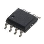
| 描述 | IC REG LDO 5V 1A 8SOIC低压差稳压器 Low Power 1 Ampere |
| 产品分类 | |
| 品牌 | Texas Instruments |
| 产品手册 | |
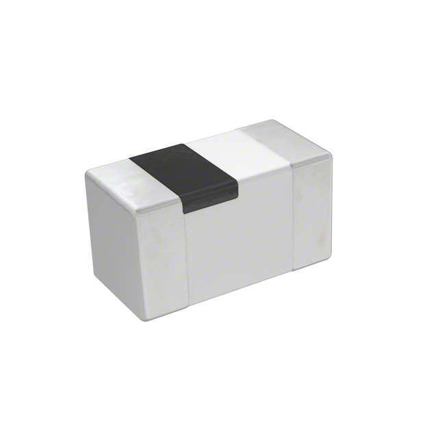
| 产品图片 |
|
| rohs | 符合RoHS无铅 / 符合限制有害物质指令(RoHS)规范要求 |
| 产品系列 | 电源管理 IC,低压差稳压器,Texas Instruments UCC381DP-5- |
| 数据手册 | |
| 产品型号 | UCC381DP-5 |
| 产品目录页面 | |
| 产品种类 | 低压差稳压器 |
| 供应商器件封装 | 8-SOIC |
| 其它名称 | 296-2820-5 |
| 包装 | 管件 |
| 单位重量 | 72.600 mg |
| 商标 | Texas Instruments |
| 回动电压—最大值 | 600 mV at 1 A |
| 安装类型 | 表面贴装 |
| 安装风格 | SMD/SMT |
| 封装 | Tube |
| 封装/外壳 | 8-SOIC(0.154",3.90mm 宽) |
| 封装/箱体 | SOIC-8 |
| 工作温度 | 0°C ~ 70°C |
| 工厂包装数量 | 75 |
| 最大工作温度 | + 70 C |
| 最大输入电压 | 9 V |
| 最小工作温度 | 0 C |
| 最小输入电压 | + 5.6 V |
| 标准包装 | 75 |
| 电压-跌落(典型值) | 0.5V @ 1A |
| 电压-输入 | 最高 9V |
| 电压-输出 | 5V |
| 电压调节准确度 | 2.5 % |
| 电流-输出 | 1A |
| 电流-限制(最小值) | - |
| 稳压器拓扑 | 正,固定式 |
| 稳压器数 | 1 |
| 系列 | UCC381-5 |
| 线路调整率 | 3 mV |
| 负载调节 | 5 mV |
| 输入偏压电流—最大 | 0.4 mA |
| 输出电压 | 5 V |
| 输出电流 | 1 A |
| 输出端数量 | 1 Output |
| 输出类型 | Fixed |


- 商务部:美国ITC正式对集成电路等产品启动337调查
- 曝三星4nm工艺存在良率问题 高通将骁龙8 Gen1或转产台积电
- 太阳诱电将投资9.5亿元在常州建新厂生产MLCC 预计2023年完工
- 英特尔发布欧洲新工厂建设计划 深化IDM 2.0 战略
- 台积电先进制程称霸业界 有大客户加持明年业绩稳了
- 达到5530亿美元!SIA预计今年全球半导体销售额将创下新高
- 英特尔拟将自动驾驶子公司Mobileye上市 估值或超500亿美元
- 三星加码芯片和SET,合并消费电子和移动部门,撤换高东真等 CEO
- 三星电子宣布重大人事变动 还合并消费电子和移动部门
- 海关总署:前11个月进口集成电路产品价值2.52万亿元 增长14.8%


.jpg)

PDF Datasheet 数据手册内容提取
UCC281-3/-5/-ADJ UCC381-3/-5/-ADJ Low Dropout 1 Ampere Linear Regulator Family FEATURES DESCRIPTION • Precision Positive Linear Voltage The UCC381-3/-5/-ADJ family of positive linear series pass regulators is Regulation tailored for low drop out applications where low quiescent power is impor- tant. Fabricated with a BiCMOS technology ideally suited for low input to • 0.5V Dropout at 1A output differential applications, the UCC381 will pass 1A while requiring • Guaranteed Reverse Input/ Output only 0.5V of input voltage headroom. Dropout voltage decreases linearly Voltage Isolation with Low Leakage with output current, so that dropout at 200mA is less than 100mV. Quies- • Low Quiescent Current Irrespective of centcurrentisalwayslessthan650µA.Topreventreversecurrentconduc- tion, on-chip circuitry limits the minimum forward voltage to typically 50mV. Load Once the forward voltage limit is reached, the input-output differential volt- • Adjustable Output Voltage Version age is maintained as the input voltage drops until undervoltage lockout dis- • Fixed Versions for 3.3V and 5V ables the regulator. Outputs UCC381-3 and UCC381-5 versions have on-chip resistor networks preset • Logic Shutdown Capability to regulate either 3.3V or 5.0V, respectively. Furthermore, remote sensing of the load voltage is possible by connecting the VOUTS pin directly at the • Short Circuit Power Limit of load.Theoutputvoltageisthenregulatedto1.5%atroomtemperatureand 3%•VIN•Current Limit better than 2.5% over temperature. The UCC381-ADJ version has a regu- • Remote Load Voltage for Accurate lated output voltage programmed by an external user-definable resistor ra- tio. Load Regulation (continued) BLOCK DIAGRAM VIN 8 1 VOUT V PUMP 4 VOUTS VOLTAGE CURRENT R2 AMPLIFIER LIMIT – – 1.3/2.1A + CURRENT + REFERENCE 2 GND 1.25V 3 GND SHUTDOWNFORFIXEDVERSIONS R1 CT* 5 6 GND 0.65V 7 GND 3%DUTYCYCLE CURRENTLIMITTIMER *ADJ VERSION ONLY REVERSEVOLTAGE R2 R1 SENSE UCC381-ADJ 0 OPEN UVLO UCC381-3 82k 50k THERMAL SHUTDOWN UCC381-5 150k 50k UDG-98112 SLUS214B -JANUARY 2001
UCC281-3/-5/-ADJ UCC381-3/-5/-ADJ ABSOLUTE MAXIMUM RATINGS CONNECTION DIAGRAMS VIN. . . . . . . . . . . . . . . . . . . . . . . . . . . . . . . . . . . . . . . . . . . . .9V CT . . . . . . . . . . . . . . . . . . . . . . . . . . . . . . . . . . . . . . .−0.3 to 3V SOIC-8(Top View) Storage Temperature. . . . . . . . . . . . . . . . . . .−65°C to +150°C DP Package Junction Temperature. . . . . . . . . . . . . . . . . . .−55°C to +150°C Lead Temperature (Soldering, 10 sec.). . . . . . . . . . . . .+300°C VOUT 1 8 VIN Currentsarepositiveinto,negativeoutofthespecifiedterminal. GND 2 7 GND ConsultPackagingSectionofDatabookforthermallimitations andconsiderationsofpackages.Allvoltagesarereferencedto GND 3 6 GND GND. VOUTS 4 5 CT* *ADJversion only DESCRIPTION (cont.) Short circuit current is internally limited. The device re- The UCC381 can be shutdown to 25µA (max) by pulling sponds to a sustained overcurrent condition by turning the CT pin low. off after a T delay. The device then stays off for a pe- ON Internal power dissipation is further controlled with ther- riod, T , that is 32 times the T delay. The device OFF ON mal overload protection circuitry. Thermal shutdown oc- then begins pulsing on and off at the T /(T +T ) ON ON OFF cursifthejunctiontemperatureexceeds165°C.Thechip duty cycle of 3%. This drastically reduces the power dis- will remain off until the temperature has dropped 20°C. sipationduringshortcircuitsuchthatheatsinking,ifatall required, must only accommodate normal operation. On TheUCC281seriesisspecifiedforoperationoverthein- the fixed output versions of the device TON is fixed at dustrial range of −40°C to +85°C, and the UCC381 se- 400µs − a guaranteed minimum. On the adjustable ver- ries is specified from 0°C to +70°C. These devices are sion an external capacitor sets the on time. The off time available in the 8 pin DP surface mount power package. is always 32 times TON. For other packaging options consult the factory. ELECTRICAL CHARACTERISTICS:Unless otherwise stated, these specifications hold for TA= 0°C to 70°C for the UCC381-X series and−40°C to +85°C for the UCC283-X series, V =V + 1.5V,I = 0mA,C = 2.2µF. C = 1500pF for IN OUT OUT OUT T theUCC381-ADJversion andV set to 5V.T = T . OUT J A PARAMETER TEST CONDITIONS MIN TYP MAX UNITS UCC381-5 Fixed 5V, 1A Family Output Voltage T = 25°C 4.925 5 5.075 V J Over Temperature 4.875 5.125 V Line Regulation V = 5.15V to 9V 1 3 mV IN Load Regulation I = 0mA to 1A 2 5 mV OUT Drop Out Voltage, VIN–VOUT IOUT= 1A,VOUT= 4.85V, TA < 85°C 0.5 0.6 V I = 200mA,V = 4.85V, TA < 85°C 100 200 mV OUT OUT Peak Current Limit V = 0V 2 3.5 A OUT OvercurrentThreshold 1 1.8 A Current Limit Duty Cycle V = 0V 3 5 % OUT OvercurrentTime Out, TON VOUT= 0V 400 750 1600 µs Quiescent Current 400 650 µA Quiescent Current in Shutdown V = 9V 10 25 µA IN Shutdown Threshold At C Input 0.25 0.65 V T Reverse Leakage Current 1V < VIN<VOUT,VOUT< 5.1V, atVOUT 75 µA UVLOThreshold V whereV passes current 2.5 2.8 3.0 V IN OUT 2
UCC281-3/-5/-ADJ UCC381-3/-5/-ADJ ELECTRICAL CHARACTERISTICS:Unless otherwise stated, these specifications hold for TA= 0°C to 70°C for the UCC381-X series and−40°C to +85°C for the UCC283-X series, V =V + 1.5V,I = 0mA,C = 2.2µF. C = 1500pF for IN OUT OUT OUT T theUCC381-ADJversion andV set to 5V.T = T . OUT J A PARAMETER TEST CONDITIONS MIN TYP MAX UNITS UCC381-3 Fixed 3.3V, 1A Family Output Voltage T = 25°C 3.25 3.3 3.35 V J Over Temperature 3.22 3.38 V Line Regulation V = 3.45V to 9V 1 3 mV IN Load Regulation I = 0mA to 1A 2 5 mV OUT Dropout Voltage, VIN-VOUT IOUT= 1A,VOUT= 3.15V, TA< 85°C 0.6 0.8 V I = 200mA,V = 3.15V, T < 85°C 100 200 mV OUT OUT A Peak Current Limit V = 0V 2 3.5 A OUT OvercurrentThreshold 1 1.8 A Current Limit Duty Cycle V = 0V 3 5 % OUT OvercurrentTime Out, TON VOUT= 0V 400 750 1600 µs Quiescent Current 400 650 µA Quiescent Current in Shutdown V = 9V 10 25 µA IN Shutdown Threshold At C Input 0.25 0.65 V T Reverse Leakage Current 1V < VIN<VOUT,VOUT< 3.35V, atVOUT 75 µA UVLOThreshold V whereV passes current 2.5 2.8 3.0 V IN OUT UCC381-ADJAdjustable Output, 1A Family Regulating Voltage atADJInput T = 25°C 1.23 1.25 1.27 V J Over Temperature 1.22 1.28 V Line Regulation, atADJInput V =V + 150mV to 9V 1 3 mV IN OUT Load Regulation, atADJInput I = 0mA to 1A 2 5 mV OUT Dropout Voltage, VIN-VOUT IOUT= 1A,VOUT= 4.85V 0.5 0.6 V I = 200mA,V = 4.85V 100 200 mV OUT OUT Peak Current Limit V = 0V 2 3.5 A OUT OvercurrentThreshold 1 1.8 A Current Limit Duty Cycle V = 0V 3 5 % OUT OvercurrentTime Out, TON VOUT= 0V, CT= 1500pF 400 1000 1600 µs Quiescent Current 400 650 µA Quiescent Current in Shutdown V = 9V 10 25 µA IN Shutdown Threshold At C Input 0.25 0.65 V T Reverse Leakage Current 1V < V <V ,V < 9V, atV 100 µA IN OUT OUT OUT Bias Current atADJInput 100 250 nA UVLOThreshold V whereV passes current 2.5 2.8 3.0 V IN OUT 3
UCC281-3/-5/-ADJ UCC381-3/-5/-ADJ PIN DESCRIPTIONS CT: For UCC381-3 and UCC381-5 versions, this is the spect to the required transient loading. For example, if shutdown pin which, when pulled low, turns off the regu- the load is very dynamic, a large capacitor will smooth lator output and puts the device in a low current state. out the response to load steps. For the UCC381-ADJ version, a capacitor is required be- tween the CT pin and GND to set the T time during VOUTS: Feedback for regulator sensing of the output ON overcurrentaccording to the following (typical) equation: voltage. For loads which are a considerable resistive dis- tancefromtheVOUTpin,theVOUTSpincanbeusedto T =660,000•C ON CT movetheresistanceintothecontrolloopoftheregulator, GND: All voltages are measured with respect to this pin. thereby effectively canceling the IR drop associated with This is the low noise ground reference input for regula- the load path. For local regulation, merely connect this tion. The output decoupling capacitor should be tied to pin directly to the VOUT pin. For the UCC381-ADJ ver- PIN 7. sion, the output voltage can be set by two external resi- torsaccording to the following relationship: VIN: Positive supply input for the regulator. Bypass this pin to GND with at least 1µF of low ESR, ESL capaci- R2 V =1.25•1+ tance if the source is located further than 1 inch from the OUT R1 device. VOUT: Output for regulator. The regulator does not re- where R1 is a resistor connected between VOUT and quire a minimum output capacitor for stability. Choose VOUTS and R2 is a resistor connected between VOUTS the appropriate size capacitor for the application with re- andGND. TYPICAL APPLICATION CIRCUIT C T SHUTDOWN NOTE2 R2 5 NOTE1 CT VOUTS 4 V IN R1 8 VIN UCC381 NOTE1 VOUT 1 OUTPUT 1.0µF GND GND GND GND C 7 6 3 2 OUT UDG-98148 Note 1: R1 and R2 for adjustable version only. For 3.3V and 5V versions connectVOUTtoVOUTS. See Pin Descriptions. Note2:C timingcapacitorisforadjustableversiononly.For3.3Vand5Vversions,theCTpinisusedtoenableorshutdown T the part. See Pin Descriptions. 4
UCC281-3/-5/-ADJ UCC381-3/-5/-ADJ APPLICATION INFORMATION Overview A capacitive load on the regulator’s output will appear as a short circuit during start-up. If the capacitance is too large, TheUCC381familyoflowdropoutlinear(LDO)regula- the output voltage will not come into regulation during the tors provide a regulated output voltage for applications initial T period and the UCC381 will enter pulsed mode with up to 1A of load current. The regulator features a ON operation. The peak current limit, T period, and load lowdropoutvoltageandshortcircuitprotection,making ON characteristics determine the maximum value of output ca- their use ideal for demanding high current applications pacitor that can be charged. For a constant current load requiring fault tolerance. the maximum output capacitance is given as follows: Short Circuit Protection C ( ) =(I −I )• TON Farads (1) The UCC381 provides unique short circuit protection OUTmax CL LOAD V OUT circuitry that reduces power dissipation during a fault. When an overload situation is detected, the device en- For worst case calculations the minimum values of on time ters a pulsed mode of operation at 3% duty cycle re- (T ) and peak current limit (I ) should be used. The ad- ON CL ducing the heat sink requirements during a fault. The justable version allows the T time to be adjusted with a ON UCC381 has two current thresholds that determine its capacitor on the CT pin: behavior during a fault as shown in Fig. 1. T ( )(µsec)=660,000•C(µFarads) (2) ONadj When the regulator current exceeds the Overcurrent Threshold for a period longer than the T , the For a resistive load (R ) the maximum output capacitor ON LOAD UCC381 shuts off for a period (T ) which is 32 times can be estimated from: OFF TON. If the short circuit current exceeds the Peak Cur- C ( ) = (3) OUTmax rent Limit, the regulator limits the current to peak cur- T rent limit during the TON period. The peak current limit ON Farads isnominally1Ampgreaterthantheovercurrentthresh- old.Theregulatorwillcontinueinpulsedmodeuntilthe l 1 fault is cleared as illustrated in Fig. 1. RLOAD • n V 1− OUT I •R CL LOAD OVERLOAD OUTPUT CURRENT PEAKCURRENT LIMIT I (nom) O OVERCURRENT THRESHOLD V O (nom) R I OL CL OUTPUT VOLTAGE TON 32TON TON 32TON TON 32TON UDG-98150 Figure 1. UCC381 short circuit timing. 5
UCC281-3/-5/-ADJ UCC381-3/-5/-ADJ APPLICATION INFORMATION (cont.) Dropout Performance Referring to the Block Diagram, the dropout voltage of Vout=3V Vout=3.3V Vout=5V theUCC381isequaltotheminimumvoltagedrop(V to 0.8 IN VOUT)acrosstheN-ChannelMOSFET.Thedropoutvolt- 0.7 age is dependent on operating conditions such as load 0.6 ) current, input and load voltages, as well as temperature. V ( 0.5 The UCC381 achieves a low Rds through the use of N (ON) VI 0.4 an internal charge-pump (V ) that drives the MOS- - PUMP T U 0.3 FET gate. Fig. 2 depicts typical dropout voltages versus O V 0.2 load current for the 3.3V and 5V versions of the part, as well as the adjustable version programmed to 3.0V. 0.1 0 Fig. 3 depicts the typical dropout performance of the ad- justable version with various output voltages and load 0.2 0.4 0.6 0.8 1 IOUT(A) currents. Operating temperatures effect the RDS(ON) and dropout Figure 2. Typical dropout vs. load current. voltage of the UCC381. Fig. 4 graphs the typical dropout for the 3.3V and 5V versions with a 3A load over tem- perature. DROP(3V) DROP(5V) Voltage Programming 0.8 Referring to the Typical Application Circuit, the output voltage for the adjustable version is externally pro- 0.7 grammed through a resistive divider at theVOUTSpin as V) ( shown. T U O0.6 V =1.25•1+R2Volts (4) -VN OUT R1 VI 0.5 For the fixed Voltage versions the resistive divider is in- ternally set, and the VOUTS pin should be connected to 0.4 the VOUT pin. The maximum programmed output volt- -40 -20 0 20 40 60 80 age for the adjustable part is constrained by the 9V ab- TEMPERATURE(°C) solute rating of the IC (including the charge pump voltage) and its ability to enhance the N-Channel MOS- Figure 4. Typical dropout vs. temperature (1A load). FET. Unless the load current is well below the 1A rating of the device, output voltages above 7V are not recom- mended. The minimum output voltage can be pro- Iout=0.2A Iout=0.5A Iout=1.0A grammed down to 1.25V, however, the input voltage 0.7 must always be greater than theUVLOof the part. 0.6 Shutdown Feature 0.5 All versions include a shutdown feature, limiting quies- V) cent current to 25µA typical. The UCC381 is shut down (T0.4 U O by pulling the CT pin to below 0.25V. As shown in the V -N0.3 applications circuit, a small logic level MOSFET or BJT VI transistor connected to the CT pin can be driven with a 0.2 digital signal, putting the device in shutdown. If the CT 0.1 pin is not pulled low, the IC will internally pull up on the pin, enabling the regulator. The CT pin should not be 0 3 3.5 4 4.5 5 forcedhigh,asthiswillinterferewiththeshortcircuitpro- tection feature. Selection of the timing capacitor for the VOUT(V) adjustable version is explained in the ShortCircuitPro- Figure 3. Typical dropoutvoltatevs.I andV OUT OUT. tectionsection. 6
UCC281-3/-5/-ADJ UCC381-3/-5/-ADJ APPLICATION INFORMATION (cont.) Thermal Design mal resistance is required by the application, the device heat sinking would need to be improved. The Packing Information section of the data book con- tains reference material for the thermal ratings of various When the UCC381 regulator is in pulsed mode, due to packages. The section also includes an excellent article an overload or short circuit in the application, the maxi- Thermal Characteristics of Surface Mount Packages, that mumaveragepower dissipation is calculated as follows: is the basis of the following discussion. P ( ) = (6) PULSE avg Topheerramtiaolnd,ensoirgmnafloarntdhepuUlsCeCd3m81odien.clIundneosrmtwaolompoedraetsiono,f (VIN −VOUT)•ICL•33T•OTN Watts the linear regulator and heat sink must dissipate power ON equal to the maximum forward voltage drop multiplied by As seen in equation 6, the average power during a fault the maximum load current. Assuming a constant current is reduced dramatically by the duty cycle, allowing the load, the expected heat rise at the regulator’s junction heat sink to be sized for normal operation. Although the can be calculated as follows: peakpowerintheregulatorduringtheT periodcanbe T =P •(θjc+θca) °C (5) ON RISE DISS significant, the thermal mass of the package will gener- ally keep the junction temperature from rising unless the WherethetaisthermalresistanceandP isthepower DISS T period is increased to tens of milliseconds. ON dissipated. The thermal resistance of both the SOIC-8 DP package (junction to case) is 22 degrees Celsius per Ripple Rejection Watt. In order to prevent the regulator from going into Even though the UCC381 linear regulators are not opti- thermal shutdown, the case to ambient theta must keep mized for fast transient applications (Refer to UC182 the junction temperature below 150C. If the LDO is “Fast LDO Linear Regulator”), they do offer significant mounted on a 5 square inch pad of 1 ounce copper, for power supply rejection at lower frequencies. Fig 5. de- example, the thermal resistance from junction to ambient picts ripple rejection performance in a typical application. becomes 40-70 degrees Celsius per Watt. If a lower ther- The performance can be improved with additional filter- ing. 90 80 ) 70 b d ( N 60 O TI C 50 10uF, E J IOUT = 100mA E 40 R E L 30 P P 1uF, IOUT = 100mA RI 20 10uF, IOUT = 1A 10 1uF, IOUT = 1A 0 1.0E+02 1.0E+03 1.0E+04 1.0E+05 FREQUENCY Figure 5. Ripple rejection vs. frequency. UNITRODE CORPORATION 7 CONTINENTAL BLVD. • MERRIMACK, NH 03054 TEL. (603) 424-2410 • FAX (603) 424-3460 7
IMPORTANT NOTICE Texas Instruments and its subsidiaries (TI) reserve the right to make changes to their products or to discontinue any product or service without notice, and advise customers to obtain the latest version of relevant information to verify, before placing orders, that information being relied on is current and complete. All products are sold subject to the terms and conditions of sale supplied at the time of order acknowledgment, including those pertaining to warranty, patent infringement, and limitation of liability. TI warrants performance of its semiconductor products to the specifications applicable at the time of sale in accordance with TI’s standard warranty. Testing and other quality control techniques are utilized to the extent TI deems necessary to support this warranty. Specific testing of all parameters of each device is not necessarily performed, except those mandated by government requirements. Customers are responsible for their applications using TI components. In order to minimize risks associated with the customer’s applications, adequate design and operating safeguards must be provided by the customer to minimize inherent or procedural hazards. TI assumes no liability for applications assistance or customer product design. TI does not warrant or represent that any license, either express or implied, is granted under any patent right, copyright, mask work right, or other intellectual property right of TI covering or relating to any combination, machine, or process in which such semiconductor products or services might be or are used. TI’s publication of information regarding any third party’s products or services does not constitute TI’s approval, warranty or endorsement thereof. Mailing Address: Texas Instruments Post Office Box 655303 Dallas, Texas 75265 Copyright 2001, Texas Instruments Incorporated