ICGOO在线商城 > 集成电路(IC) > PMIC - AC-DC 转换器,离线开关 > UCC28600DG4

 Datasheet下载
- 型号: UCC28600DG4
- 制造商: Texas Instruments
- 库位|库存: xxxx|xxxx
- 要求:
| 数量阶梯 | 香港交货 | 国内含税 |
| +xxxx | $xxxx | ¥xxxx |
查看当月历史价格
查看今年历史价格
UCC28600DG4产品简介:
ICGOO电子元器件商城为您提供UCC28600DG4由Texas Instruments设计生产,在icgoo商城现货销售,并且可以通过原厂、代理商等渠道进行代购。 UCC28600DG4价格参考¥4.57-¥10.36。Texas InstrumentsUCC28600DG4封装/规格:PMIC - AC-DC 转换器,离线开关, Converter Offline Flyback Topology 40kHz ~ 130kHz 8-SOIC。您可以下载UCC28600DG4参考资料、Datasheet数据手册功能说明书,资料中有UCC28600DG4 详细功能的应用电路图电压和使用方法及教程。
UCC28600DG4是德州仪器(Texas Instruments)生产的一款高效、高集成度的离线式开关电源控制器,属于PMIC(电源管理集成电路)中的AC-DC转换器类别。该器件主要用于将交流电(AC)转换为直流电(DC),广泛应用于各种需要稳定直流电源输出的场景中。以下是其主要应用场景:

1. 消费电子设备:如电视、显示器、音响系统等家用电器中,UCC28600DG4可以提供高效的电源转换,确保这些设备在不同输入电压条件下都能获得稳定的直流电源。

2. 计算机及外设:包括台式电脑、笔记本电脑适配器、打印机、扫描仪等,UCC28600DG4能够为这些设备提供可靠且高效的电源解决方案,支持宽范围的输入电压,并具备良好的电磁兼容性(EMC)性能。

3. 工业控制系统:例如工厂自动化设备、PLC(可编程逻辑控制器)、传感器和执行器等,UCC28600DG4可以在工业环境中提供稳定的电源供应,适应较宽的工作温度范围和恶劣的工作条件。

4. 通信设备:如路由器、交换机、基站等通信基础设施中,UCC28600DG4可以确保这些设备在不同电网条件下稳定运行,同时具备低待机功耗特性,有助于节能减排。

5. 医疗设备:在医疗仪器和设备中,UCC28600DG4提供了可靠的电源管理方案,确保设备在关键操作时的稳定性与安全性,符合相关的安全标准。

总之,UCC28600DG4凭借其高效能、高可靠性以及灵活的应用特性,成为众多领域中不可或缺的电源管理解决方案之一。它不仅能满足不同应用场景的需求,还能帮助设计者简化电路设计,降低成本,提高系统的整体性能。
| 参数 | 数值 |
| 产品目录 | 集成电路 (IC)半导体 |
| 描述 | IC CTRLR PWM GREEN CM OVP 8SOIC交流/直流转换器 Quasi Res Flyback Green Mode Cntrlr |
| 产品分类 | |
| 品牌 | Texas Instruments |
| 产品手册 | |
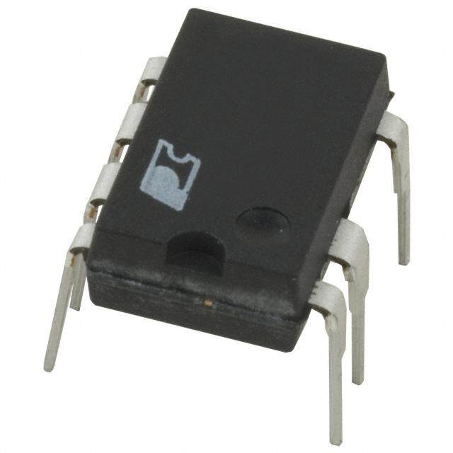
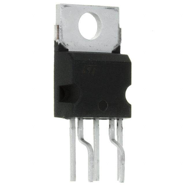
| 产品图片 |
|
| rohs | 符合RoHS无铅 / 符合限制有害物质指令(RoHS)规范要求 |
| 产品系列 | 电源管理 IC,交流/直流转换器,Texas Instruments UCC28600DG4- |
| 数据手册 | |
| 产品型号 | UCC28600DG4 |
| 产品种类 | 交流/直流转换器 |
| 供应商器件封装 | 8-SOIC |
| 功率(W) | - |
| 包装 | 管件 |
| 单位重量 | 72.600 mg |
| 占空比-最大 | 99 % |
| 参考设计库 | http://designs.digikey.com/library/4294959904/4294959863/366 |
| 商标 | Texas Instruments |
| 安装风格 | SMD/SMT |
| 封装 | Tube |
| 封装/外壳 | 8-SOIC(0.154",3.90mm 宽) |
| 封装/箱体 | SOIC-8 |
| 工作温度 | -40°C ~ 105°C |
| 工作温度范围 | - 40 C to + 105 C |
| 工厂包装数量 | 75 |
| 开关频率 | 40 kHz to 130 kHz |
| 拓扑结构 | Flyback |
| 标准包装 | 75 |
| 电压-击穿 | - |
| 电压-输入 | 9.3 V ~ 32 V |
| 电压-输出 | - |
| 电源电流 | 5 mA |
| 类型 | Current Mode PWM Controllers |
| 系列 | UCC28600 |
| 绝缘 | Isolated |
| 输入/电源电压—最大值 | 32 V |
| 输入/电源电压—最小值 | 9.3 V |
| 输出电压 | - |
| 输出电流 | 1.2 A |
| 输出端数量 | 1 Output |
| 输出隔离 | 隔离 |
| 配用 | /product-detail/zh/UCC28600EVM-65W/296-29101-ND/1911775/product-detail/zh/UCC28600EVM/296-23117-ND/1805637 |
| 频率范围 | 40kHz ~ 130kHz |


- 商务部:美国ITC正式对集成电路等产品启动337调查
- 曝三星4nm工艺存在良率问题 高通将骁龙8 Gen1或转产台积电
- 太阳诱电将投资9.5亿元在常州建新厂生产MLCC 预计2023年完工
- 英特尔发布欧洲新工厂建设计划 深化IDM 2.0 战略
- 台积电先进制程称霸业界 有大客户加持明年业绩稳了
- 达到5530亿美元!SIA预计今年全球半导体销售额将创下新高
- 英特尔拟将自动驾驶子公司Mobileye上市 估值或超500亿美元
- 三星加码芯片和SET,合并消费电子和移动部门,撤换高东真等 CEO
- 三星电子宣布重大人事变动 还合并消费电子和移动部门
- 海关总署:前11个月进口集成电路产品价值2.52万亿元 增长14.8%


PDF Datasheet 数据手册内容提取
Product Sample & Technical Tools & Support & Reference Folder Buy Documents Software Community Design UCC28600 SLUS646K–NOVEMBER2005–REVISEDAUGUST2015 UCC28600 8-Pin Quasi-Resonant Flyback Green-Mode Controller 1 Features 3 Description • Green-ModeControllerWithAdvancedEnergy The UCC28600 is a PWM controller with advanced 1 energy features to meet stringent world-wide energy SavingFeatures efficiencyrequirements. • Quasi-ResonantModeOperationforReduced EMIandLowSwitchingLosses(Low-Voltage UCC28600 integrates built-in advanced energy saving features with high-level protection features to ValleySwitching) provide cost-effective solutions for energy-efficient • LowStandbyCurrentforMinimumSystemNo- power supplies. UCC28600 incorporates frequency LoadPowerConsumption fold-back and green-mode operation to reduce the • LowStart-upCurrent:25-μAMaximum switchinglossesatlight-loadandno-loadconditions. • ProgrammableLineandLoadOver-Voltage UCC28600 is available in the 8-pin SOIC package. Protection Operating junction temperature range is –40°C to • InternalOver-TemperatureProtection +105°C. • CurrentLimitProtection The UCC28600 Design Calculator, (SLVC104), – Cycle-by-CyclePowerLimit located in the Tools and Software section of the UCC28600 product folder, provides a user-interactive – Primary-SideOver-CurrentHiccupRestart iterative process for selecting recommended Mode componentvaluesforanoptimaldesign. • 1-ASink,–0.75-ASourceTrueDrive™GateDrive Output DeviceInformation (1) • ProgrammableSoft-Start PARTNUMBER PACKAGE BODYSIZE(NOM) • Green-ModeStatusPin(PFCDisableFunction) UCC28600 SOIC(8) 4.90mm×3.91mm (1) For all available packages, see the orderable addendum at 2 Applications theendofthedatasheet. • BiasSuppliesforLCD-Monitors,LCD-TV,PDP- TV,andSetTopBoxes • AC-to-DCAdaptersandOff-LineBatteryChargers • EnergyEfficientPowerSuppliesupto200W TypicalApplicationDiagram Primary Secondary CBULK RSU NP NS CB NB 18V CSS UCC28600 ROVP1 1 SS STATUS 8 CVDD UCC28051 1 VO_SNS VCC 8 2 FB OVP 7 ROVP2 2 COMP DRV 7 3 CS VDD 6 3 MULTIN GND 6 4 GND OUT 5 Feedback M1 4 CS ZCD 5 CBP RPL RCS TL431 1 An IMPORTANT NOTICE at the end of this data sheet addresses availability, warranty, changes, use in safety-critical applications, intellectualpropertymattersandotherimportantdisclaimers.PRODUCTIONDATA.
UCC28600 SLUS646K–NOVEMBER2005–REVISEDAUGUST2015 www.ti.com Table of Contents 1 Features.................................................................. 1 7.4 DeviceFunctionalModes........................................18 2 Applications........................................................... 1 8 ApplicationandImplementation........................ 21 3 Description............................................................. 1 8.1 ApplicationInformation............................................21 4 RevisionHistory..................................................... 2 8.2 TypicalApplication .................................................21 8.3 Do'sandDon'ts ......................................................33 5 PinConfigurationandFunctions......................... 3 9 PowerSupplyRecommendations...................... 34 6 Specifications......................................................... 4 10 Layout................................................................... 34 6.1 AbsoluteMaximumRatings......................................4 6.2 ESDRatings ............................................................4 10.1 LayoutGuidelines.................................................34 6.3 RecommendedOperatingConditions.......................4 10.2 LayoutExample....................................................35 6.4 ThermalInformation..................................................4 11 DeviceandDocumentationSupport................. 36 6.5 ElectricalCharacteristics...........................................5 11.1 DeviceSupport ....................................................36 6.6 TimingRequirements................................................6 11.2 DocumentationSupport .......................................36 6.7 TypicalCharacteristics..............................................7 11.3 Trademarks...........................................................36 7 DetailedDescription.............................................. 8 11.4 ElectrostaticDischargeCaution............................36 7.1 Overview...................................................................8 11.5 Glossary................................................................36 7.2 FunctionalBlockDiagram.........................................8 12 Mechanical,Packaging,andOrderable Information........................................................... 37 7.3 FeatureDescription.................................................11 4 Revision History NOTE:Pagenumbersforpreviousrevisionsmaydifferfrompagenumbersinthecurrentversion. ChangesfromRevisionJ(July2011)toRevisionK Page • AddedPinConfigurationandFunctionssection,ESDtable,FeatureDescriptionsection,DeviceFunctionalModes, ApplicationandImplementationsection,PowerSupplyRecommendationssection,Layoutsection,Deviceand DocumentationSupportsection,andMechanical,Packaging,andOrderableInformationsection. .................................... 1 • ChangedFunctionalBlockdiagram........................................................................................................................................ 8 • ChangedControlFlowChartdiagram.................................................................................................................................. 11 • ChangedQRDetectDetailsimage...................................................................................................................................... 13 • ChangedOscillatorDetailsimage........................................................................................................................................ 14 • ChangedFaultLogicDetailsimage...................................................................................................................................... 16 • ChangedModeControlwithFBPinVoltageimage. ........................................................................................................... 18 • ChangedOperationModeSwitchingFrequenciesimage. .................................................................................................. 19 ChangesfromRevisionH(November2005)toRevisionI Page • ChangedEquation35 .......................................................................................................................................................... 29 2 SubmitDocumentationFeedback Copyright©2005–2015,TexasInstrumentsIncorporated ProductFolderLinks:UCC28600
UCC28600 www.ti.com SLUS646K–NOVEMBER2005–REVISEDAUGUST2015 5 Pin Configuration and Functions DPackage 8-PinSOIC TopView SS 1 8 STATUS FB 2 7 OVP CS 3 6 VDD GND 4 5 OUT PinFunctions PIN I/O DESCRIPTION NAME NO. Currentsenseinput.Alsoprogramspowerlimit,andusedtocontrolmodulationandactivate overcurrentprotection.TheCSvoltageinputoriginatesacrossacurrentsenseresistorand CS 3 I ground.Powerlimitisprogrammedwithaneffectiveseriesresistancebetweenthispinand thecurrentsenseresistor. FeedbackinputorcontrolinputfromtheoptocouplertothePWMcomparatorusedtocontrol thepeakcurrentinthepowerMOSFET.Aninternal20-kΩresistorisbetweenthispinand theinternal5-Vregulatedvoltage.Connectthecollectorofthephoto-transistorofthe FB 2 I feedbackoptocouplerdirectlytothispin;connecttheemitterofthephoto-transistortoGND. Thevoltageofthispincontrolsthemodeofoperationinoneofthethreemodes:quasi resonant(QR),frequencyfoldbackmode(FFM)andgreenmode(GM). Groundforinternalcircuitry.Connectaceramic0.1-μFbypasscapacitorbetweenVDDand GND 4 – GND,withthecapacitorasclosetothesetwopinsaspossible. 1-Asink(TrueDrive™)and0.75-Asourcegatedriveoutput.Thisoutputdrivesthepower OUT 5 O MOSFETandswitchesbetweenGNDandthelowerofVDDorthe13-Vinternaloutput clamp. Overvoltageprotection(OVP)inputsensesline-OVP,load-OVPandtheresonanttroughfor OVP 7 I QRturn-on.Detectline,loadandresonantconditionsusingtheprimarybiaswindingofthe transformer,adjustsensitivitywithresistorsconnectedtothispin. Soft-startprogrammingpin.Programthesoft-startratewithacapacitortoground;therateis determinedbythecapacitanceandtheinternalsoft-startchargecurrent.Thesoft-start capacitorshouldbeplacedascloseaspossibletotheSSpinandGND,keepingtrace SS 1 I lengthtoaminimum.AllfaultsdischargetheSSpintoGNDthroughaninternalMOSFET withanR ofapproximately100Ω.Theinternalmodulatorcomparatorreactstothe DS(on) lowestoftheSSvoltage,theinternalFBvoltageandthepeakcurrentlimit. ACTIVEHIGHopendrainsignalthatindicatesthedevicehasenteredstandbymode.This STATUS 8 O pincanbeusedtodisablethePFCcontrolcircuit(highimpedance=greenmode).STATUS pinishighduringUVLO,(VDD<start-upthreshold),andsoftstart,(SS<FB). Providespowertothedevice.Useaceramic0.1-μFby-passcapacitorforhigh-frequency filteringoftheVDDpin,asdescribedintheGNDpindescription.Operatingenergyisusually VDD 6 I deliveredfromauxiliarywinding.Topreventhiccupoperationduringstart-up,alargerenergy storagecapisalsoneededbetweenVDDandGND. Copyright©2005–2015,TexasInstrumentsIncorporated SubmitDocumentationFeedback 3 ProductFolderLinks:UCC28600
UCC28600 SLUS646K–NOVEMBER2005–REVISEDAUGUST2015 www.ti.com 6 Specifications 6.1 Absolute Maximum Ratings overoperatingfree-airtemperaturerange(unlessotherwisenoted) (1) MIN MAX UNIT VDD Supplyvoltagerange,I <20mA 32 V DD I Supplycurrent 20 mA DD I Outputsinkcurrent(peak) 1.2 A OUT(sink) I Outputsourcecurrent(peak) –0.8 A OUT(source) Analoginputs:FB,CS,SS –0.3 6.0 V V –1.0 6.0 V OVP I –1.0 mA OVP(source) V VDD=0Vto30V 30 V STATUS Powerdissipation,SOIC-8package,T =25°C 650 mW A T Leadtemperature1,6mm(1/16inch)fromcasefor10seconds 300 °C LEAD T Operatingjunctiontemperature –55 150 °C J T Storagetemperature –65 150 °C stg (1) StressesbeyondthoselistedunderAbsoluteMaximumRatingsmaycausepermanentdamagetothedevice.Thesearestressratings only,whichdonotimplyfunctionaloperationofthedeviceattheseoranyotherconditionsbeyondthoseindicatedunderRecommended OperatingConditions.Exposuretoabsolute-maximum-ratedconditionsforextendedperiodsmayaffectdevicereliability. 6.2 ESD Ratings VALUE UNIT Humanbodymodel(HBM),perANSI/ESDA/JEDECJS-001,all pins (1) ±2000 V V Electrostaticdischarge (ESD) Chargeddevicemodel(CDM),perJEDECspecification JESD22-C101,allpins (2) ±1500 V (1) JEDECdocumentJEP155statesthat500-VHBMallowssafemanufacturingwithastandardESDcontrolprocess. (2) JEDECdocumentJEP157statesthat250-VCDMallowssafemanufacturingwithastandardESDcontrolprocess. 6.3 Recommended Operating Conditions overoperatingfree-airtemperaturerange(unlessotherwisenoted) MIN NOM MAX UNIT VDD Inputvoltage 21 V C VDDbypasscapacitor 0.1 1.0 μF VDD C FBfiltercapacitor 390 pF FB T Operatingjunctiontemperature –40 105 °C J 6.4 Thermal Information UCC28600 THERMALMETRIC (1) D(SOIC) UNIT 8PINS R Junction-to-ambientthermalresistance 108.9 °C/W θJA R Junction-to-case(top)thermalresistance 55.5 °C/W θJC(top) R Junction-to-boardthermalresistance 48.9 °C/W θJB ψ Junction-to-topcharacterizationparameter 10.5 °C/W JT ψ Junction-to-boardcharacterizationparameter 48.5 °C/W JB (1) Formoreinformationabouttraditionalandnewthermalmetrics,seetheSemiconductorandICPackageThermalMetricsapplication report,SPRA953. 4 SubmitDocumentationFeedback Copyright©2005–2015,TexasInstrumentsIncorporated ProductFolderLinks:UCC28600
UCC28600 www.ti.com SLUS646K–NOVEMBER2005–REVISEDAUGUST2015 6.5 Electrical Characteristics VDD=15V,0.1-μFcapacitorfromVDDtoGND,3.3-nFcapacitorfromSStoGNDchargedover3.5V,500-Ωresistorfrom OVPto–0.1V,FB=4.8V,STATUS=notconnected,1-nFcapacitorfromOUTtoGND,CS=GND,T =–40°Cto+105°C, A (unlessotherwisenoted) PARAMETER TESTCONDITIONS MIN TYP MAX UNIT I Start-upcurrent VDD=V –0.3V 12 25 μA STARTUP UVLO I Standbycurrent V =0V 350 550 μA STANDBY FB Notswitching 2.5 3.5 mA I Operatingcurrent DD 130kHz,QRmode 5.0 7.0 mA VDDclamp FB=GND,I =10mA 21 26 32 V DD UNDERVOLTAGELOCKOUT VDD Start-upthreshold VDDincreasing 10.3 13.0 15.3 V (uvlo) VDD Stopthreshold VDDdecreasing 6.3 8 9.3 V (uvlo) ΔVDD Hysteresis 4.0 5.0 6.0 V (uvlo) PWM(RAMP) (1) D Minimumdutycycle V =GND,V =2V 0% MIN SS FB D Maximumdutycycle QRmode,f =max,(openloop) 99% MAX S OSCILLATOR(OSC) f MaximumQRandDCMfrequency 117 130 143 kHz QR(max) f MinimumQRandFFMfrequency V =1.3V 32 40 48 kHz QR(min) FB f Softstartfrequency V =2.0V 32 40 48 kHz SS SS dT /dFB VCOgain T for1.6V<V <1.8V –38 –30 –22 μs/V S S FB FEEDBACK(FB) R Feedbackpullupresistor 12 20 28 kΩ FB V FB,noload QRmode 3.30 4.87 6.00 V FB Green-modeONthreshold V threshold 0.3 0.5 0.7 V FB Green-modeOFFthreshold V threshold 1.2 1.4 1.6 V FB Green-modehysteresis V threshold 0.7 0.9 1.1 V FB FBthresholdburst-ON V duringgreenmode 0.3 0.5 0.7 V FB FBthresholdburst-OFF V duringgreenmode 0.5 0.7 0.9 V FB BurstHysteresis V duringgreenmode 0.13 0.25 0.42 V FB STATUS R STATUSonresistance V =1V 1.0 2.4 3.8 kΩ DS(on) STATUS I STATUSleakage/offcurrent V =0.44V,V =15V –0.1 2.0 μA STATUS(leakage) FB STATUS (1) R andC arenotconnectedinthecircuitformaximumandminimumdutycycletests,currentsensetests,andpowerlimittests. CST CST Copyright©2005–2015,TexasInstrumentsIncorporated SubmitDocumentationFeedback 5 ProductFolderLinks:UCC28600
UCC28600 SLUS646K–NOVEMBER2005–REVISEDAUGUST2015 www.ti.com Electrical Characteristics (continued) VDD=15V,0.1-μFcapacitorfromVDDtoGND,3.3-nFcapacitorfromSStoGNDchargedover3.5V,500-Ωresistorfrom OVPto–0.1V,FB=4.8V,STATUS=notconnected,1-nFcapacitorfromOUTtoGND,CS=GND,T =–40°Cto+105°C, A (unlessotherwisenoted) PARAMETER TESTCONDITIONS MIN TYP MAX UNIT CURRENTSENSE(CS) (1) A Gain=ΔV /ΔV QRmode 2.5 V/V CS(FB) FB CS Shutdownthreshold V =2.4V,V =0V 1.13 1.25 1.38 V FB SS CSdischargeimpedance CS=0.1V,V =0V 25 115 250 Ω SS V CSoffset SSmode,V ≤2.0V 0.35 0.40 0.45 V CS(os) SS POWERLIMIT(PL) (1) I CScurrent OVP=–300μA –165 –150 –135 μA PL(cs) PeakCSvoltage QRmode 0.70 0.81 0.92 V V PLthreshold PeakCSvoltage+CSoffset 1.05 1.20 1.37 V PL SOFTSTART(SS) I Softstartchargecurrent V =GND –8.3 –6.0 –4.5 μA SS(chg) SS I Softstartdischargecurrent V =0.5V 2.0 5.0 10 mA SS(dis) SS V SwitchingONthreshold Outputswitchingstart 0.8 1.0 1.2 V SS OVERVOLTAGEPROTECTION(OVP) I Lineovervoltageprotection I threshold,OUT=HI –512 –450 –370 μA OVP(line) OVP V =4.8V,V =5.0V, V OVPvoltageatOUT=HIGH FB SS –125 –25 mV OVP(on) I ,=–300μA OVP(on) V Loadovervoltageprotection V threshold,OUT=LO 3.37 3.75 4.13 V OVP(load) OVP THERMALPROTECTION(TSP) Thermalshutdown(TSP) temperature (2) 130 140 150 °C Thermalshutdownhysteresis 15 °C (2) Ensuredbydesign.Notproductiontested. 6.6 Timing Requirements MIN NOM MAX UNIT CURRENTSENSE(CS) (1) CStooutputdelaytime(powerlimit),CS=1.0V 100 175 300 ns PULSE CStooutputdelaytime(overcurrentfault),CS=1.45V 50 100 150 ns PULSE OUT t Risetime,10%to90%of13-VtypicalOUTclamp 50 75 ns RISE t Falltime 10 20 ns FALL (1) R andC arenotconnectedinthecircuitformaximumandminimumdutycycletests,currentsensetests,andpowerlimittests. CST CST 6 SubmitDocumentationFeedback Copyright©2005–2015,TexasInstrumentsIncorporated ProductFolderLinks:UCC28600
UCC28600 www.ti.com SLUS646K–NOVEMBER2005–REVISEDAUGUST2015 6.7 Typical Characteristics 31 142 29 Hz 137 VDD – Clamp Voltage – V 2257 – Switching Frequency – k 112372 23 f S 122 21 117 –50 0 50 100 150 –50 0 50 100 150 TJ – Temperature – °C TJ – Temperature – °C Figure1.ClampVoltagevs.Temperature Figure2.SwitchingFrequencyvs.Temperature -372 0.95 V S Voltage – 0.90 eshold - AP --431922 d, QR Mode, Peak C 00..8805 oltage Protection Thr --443522 PL Threshol 0.75 I Over-VOVP --449722 0.70 –50 0 50 100 150 -512 TJ – Temperature – °C -50 0 50 100 150 TJ - Temperature - °C Figure3.PLThresholdvs.Temperature Figure4.Over-VoltageProtectionThresholdvs. Temperature Copyright©2005–2015,TexasInstrumentsIncorporated SubmitDocumentationFeedback 7 ProductFolderLinks:UCC28600
UCC28600 SLUS646K–NOVEMBER2005–REVISEDAUGUST2015 www.ti.com 7 Detailed Description 7.1 Overview The UCC28600 is a flyback power supply controller that operates in different operating modes, modulating the peak primary current and/or the switching frequency, depending upon the line and load conditions. The controller will operate in burst mode operation, or green mode (GM) driving the primary side MOSFET with packets of 40-kHzpulses,atfixedpeakprimarycurrentforlight-loadconditions.Astheloadincreases,the40-kHzswitching will become consistent and the controller will transition to frequency fold-back mode (FFM), where the peak primary current is held constant and the switching frequency is modulated from 40 kHz up to 130 kHz, in order to maintainregulation.Athigherloads,theUCC28600willoperateineitherDCM,wherethepeakprimarycurrentis modulated but the switching frequency is maintained at its maximum value, or quasi-resonant mode (QRM), wheretheswitchingfrequencyandthepeakprimarycurrentarebothmodulatedinordertomaintainregulation. 7.2 Functional Block Diagram CBULK RSU RVDD CVDD ROVP1 VDD OVP ROVP2 6 7 UCC28600 REF 5.0 VDD_OK + 26 V ILINE VREF 13/8 V On-Chip Fault Logic Thermal Shutdown REF_OK VDD_OK QR DETEC_T___ OVR_T LOAD_OVP LOAD_OVP OUT VDD STATUS 8 STATUS LINE_OVP LINE_OVP SS_DIS CS CS VREF SS_MODE BURST BURST 6PA RUN QR_DONE OSCILLATOR SS 1 RUN REF CSS SS_MODEQR_DONE 5 OUT OSC_CL CLK DSETQ + GREEN MODE CLRQ OSC_CL FB FB_CLAMP PL CS REF 1.2 V 3 GAIN = 1/2.5 Modulation 20 k: Comparison ILINE RPL Feedback FB 2 + 2 RCS 1.5RR VCS(os) GND 4 + 400 mV 8 SubmitDocumentationFeedback Copyright©2005–2015,TexasInstrumentsIncorporated ProductFolderLinks:UCC28600
UCC28600 www.ti.com SLUS646K–NOVEMBER2005–REVISEDAUGUST2015 Functional Block Diagram (continued) 7.2.1 TerminalComponents Table1. TerminalComponents PIN I/O DESCRIPTION (1) (2) NAME NO. (cid:11)VPL(cid:16)VCS(os)(cid:11)ICS(2)(cid:16)ICS(1)(cid:12)(cid:12) RCS ICS(2)(cid:16)IP(1)(cid:16)ICS(1)(cid:16)IP(2) (1) (cid:11)VPL(cid:16)VCS(os)(cid:11)IP(2)(cid:16)IP(1)(cid:12)(cid:12) RPL ICS(1)(cid:16)IP(2)(cid:16)ICS(2)(cid:16)IP(1) (2) where: CS 3 I • I isthepeakprimarycurrentatlowline,fullload (2) P(1) • I isthepeakprimarycurrentathighline,fullload (2) P(2) • I isthepowerlimitcurrentthatissourcedattheCSpinatlow-linevoltage (2) CS(1) • I isthepowerlimitcurrentthatissourcedattheCSpinathigh-linevoltage (2) CS(2) • V isthePowerLimit(PL)threshold (1) PL • V istheCSoffsetvoltage (1) CS(os) FB 2 I Opto-isolatorcollector GND 4 – BypasscapacitortoVDD,C =0.1μF BP OUT 5 O PowerMOSFETgate ROVP1 IOVP1(line)§¨©NNPBVBULK(ov)·¸¹ (3) § · ROVP2 ROVP1¨¨¨¨©NNBP(cid:11)VOUT(shutdVoOwVnP)((cid:14)linVe)F(cid:12)(cid:16)VOVP(load)¸¸¸¸¹ (4) where: OVP 7 I • I isOVP currentthreshold (1) OVP(line) line • V istheallowedinputover-voltagelevel (2) BULK(ov) • V isOVP (1) OVP(load) load • V istheallowedoutputover-voltagelevel (2) OUT(shutdown) • V istheforwardvoltageofthesecondaryrectifier F • N isthenumberofturnsonthebiaswinding (2) B • N isthenumberofturnsonthesecondarywindings (2) S • N isthenumberofturnsontheprimarywindings (2) P CSS!ISSuAtSCSS(m(FinB))(cid:11)ud(cid:11)uVePpLo(cid:16)wVeCrlSim(osit)(cid:12)(cid:12) (5) wheret isthegreaterof: SS(min) tSS(min) ª««¬(cid:16)RLOAD2(ss)COUTlnRLVOOAUDT(s(cid:16)s)P'OVUOTU(Tm(asxte)lpim)it»»¼º (6) or SS 1 I tSS(min) ª««¬COU2TPVLIOMUT2º»»¼ (7) • R istheeffectiveloadimpedanceduringsoft-start (2) LOAD(ss) • ΔV istheallowedchangeinV duetoaloadstep (2) OUT(step) OUT • P Programmedpowerlimitlevel,inW (2) OUT(maxlimit) • A isthecurrentsensegain (1) CS(FB) • V istheCSoffsetvoltage (1) CS(os) • I isthesoft-startchargingcurrent (1) SS • V isthepowerlimitthreshold (1) PL (1) RefertotheElectricalCharacteristicsforconstantparameters. (2) RefertotheUCC28600DesignCalculator(SLVC104)orlaboratorymeasurementsforcurrents,voltagesandtimesintheoperational circuit. Copyright©2005–2015,TexasInstrumentsIncorporated SubmitDocumentationFeedback 9 ProductFolderLinks:UCC28600
UCC28600 SLUS646K–NOVEMBER2005–REVISEDAUGUST2015 www.ti.com Functional Block Diagram (continued) Table1. TerminalComponents(continued) PIN I/O DESCRIPTION (1) (2) NAME NO. RST2 ISTATVUBSE((loefafk)age) (8) RST1 RST2uª««¬VDD(uvlo(cid:16)on)§¨¨©(cid:16)§¨©EVICsBCaEt(·¸¹saut)R(cid:16)SRT2D·¸¸¹S((cid:14)onV)BuE§¨©(sEIaCst)Cat·¹¸º»»¼(cid:16)RDS(on)VBE(sat) (9) STATUS 8 O where: • β isthegainoftransistorQ insaturation SAT ST • V isthebase-emittervoltageoftransistorQ insaturation BE(sat) ST • VDD isthestart-upthreshold (1) (uvlo-on) • I isthecollectorcurrentofQ CC ST • I isthemaximumleakage/offcurrentoftheSTATUSpin (1) STATUS(leakage) • V isthemaximumallowablevoltageacrossthebaseemitterjunctionthatwillnotturnQ on BE(off) ST • R istheR ofSTATUS (1) DS(on) DS(on) C isthegreaterof: VDD CVDD ª««¬(cid:11)IDD(cid:14)CISSVOUT(hi)fQR(max)(cid:12)'VTDBUDR(bSuTrst)º»»¼ (10) or CVDD ª««¬(cid:11)IDD(cid:14)CISSVOUT(hi)fQR(max)(cid:12)'VDTDS(Suvlo)º»»¼ (11) RVDD §¨©4S·¸¹§¨©NNBP·¸¹§¨¨©VDS1(os)IfDQDR(m(cid:14)aCx)ISSLVLEOAUKTA(hGi)EfQ(cid:11)RC(Dma(cid:14)x)CSNUB(cid:12)·¸¸¹ (12) RSU VISBTUALRKT(mUiPn) (13) where: VDD 6 I • I istheoperatingcurrentoftheUCC28600 (1) DD • C istheinputcapacitanceofMOSFETM ISS 1 • V isVOHoftheOUTpin,either13V(typ)V clamporlessasmeasured OUT(hi) OUT • f isf athighline,maximumload (1) QR(max) S • T isthemeasuredburstmodeperiod BURST • ΔVDD istheallowedV rippleduringburstmode (burst) DD • ΔVDD istheUVLOhysteresis (1) (uvlo) • V istheamountofdrain-sourceovershootvoltage DS1(os) • L istheleakageinductanceoftheprimarywinding LEAKAGE • C isthetotaldrainnodecapacitanceofMOSFETM D 1 • I isI start-upcurrentoftheUCC28600 (1) STARTUP DD • C isthesnubbercapacitorvalue SNUB • t isthesoftstartchargetime (2) SS 10 SubmitDocumentationFeedback Copyright©2005–2015,TexasInstrumentsIncorporated ProductFolderLinks:UCC28600
UCC28600 www.ti.com SLUS646K–NOVEMBER2005–REVISEDAUGUST2015 7.3 Feature Description The UCC28600 is a multi-mode controller, as illustrated in Figure 5 and Figure 12. The mode of operation depends upon line and load conditions. Under all modes of operation, the UCC28600 terminates the OUT = HI signal based on the switch current. Thus, the UCC28600 always operates in current mode control so that the powerMOSFETcurrentisalwayslimited. Under normal operating conditions, the FB pin commands the operating mode of the UCC28600 at the voltage thresholds shown in the control flow chart, Figure 11. Soft-start and fault responses are the exception. During soft start, the converter switching frequency is fixed at 40 kHz and FB is set to 5V. The soft-start mode is latched-OFF when V becomes greater than V for the first time after UVLO . The soft-start state cannot be SS FB ON recovereduntilafterpassingUVLO ,andthen,UVLO . OFF ON From 100% to approximately 30% full rated power the UCC28600 controls the converter in quasi-resonant mode (QRM) or discontinuous conduction mode (DCM), where DCM operation is at the clamped maximum switching frequency (130 kHz). For loads that are between approximately 30% and 10% full rated power, the converter operates in frequency foldback mode (FFM), where the peak switch current is constant and the output voltage is regulated by modulating the switching frequency for a given and fixed V . Effectively, operation in FFM results in IN the application of constant volt-seconds to the flyback transformer each switching cycle. Voltage regulation in FFM is achieved by varying the switching frequency in the range from 130 kHz to 40 kHz. For extremely light loads(belowapproximately10%fullratedpower),theconverteriscontrolledusingburstsof40-kHzpulses. START RUN = 0 Y STATUS = 1 N VCC > 13 V? RVECCF << 84 VV?? N OVP = 1? Y RUN = 1 OT = 1? STATUS = 1 OC = 1? RUN = 0 Soft Start Monitor VFB VFB < 1.4 V 1.4 V < VFB < 2.0 V 2.0 V < VFB Fixed V-sec STATUS = 0 STATUS = 0 40 kHz (In Run-Mode) (In Run-Mode) N Fixed V-sec Quasi-Resonant VFB < 0.5 V Freq. Foldback Mode or DCM (Light Load) (Normal Load) Y Zero Pulses STATUS = 1 (In Green-Mode) STATUS = 0 Fixed V-sec (In Run-Mode) 40 kHz Burst Y N N Y Y N VFB > 1.4 V VFB > 0.7 V VFB > 0.5 V Figure5. ControlFlowChart Copyright©2005–2015,TexasInstrumentsIncorporated SubmitDocumentationFeedback 11 ProductFolderLinks:UCC28600
UCC28600 SLUS646K–NOVEMBER2005–REVISEDAUGUST2015 www.ti.com Feature Description (continued) Details of the functional boxes in the Block Diagram/Typical Application drawing are shown in Figure 8, Figure 6, Figure 7 and Figure 10. These figures conceptualize how the UCC28600 executes the command of the FB voltage to have the responses that are shown in Figure 11, Figure 5 and Figure 12. The details of the functional boxes also conceptualize the various fault detections and responses that are included in the UCC28600. During all modes of operation, this controller operates in current mode control. This allows the UCC28600 to monitor the FBvoltagetodetermineandrespondtothevaryingloadlevelssuchasheavy,lightorultra-light. Quasi-resonant mode and DCM occurs for feedback voltages V between 2.0 V and 4.0 V, respectively. In turn, FB theCSvoltageiscommandedtobebetween0.4Vand0.8V.Acycle-by-cyclepowerlimitimposesafixed0.8-V limit on the CS voltage. An overcurrent shutdown threshold in the fault logic gives added protection against high- current, slew-rate shorted winding faults, shown in Figure 10. The power limit feature in the QR DETECT circuit of Figure 7 adds an offset to the CS signal that is proportional to the line voltage. The power limit feature is programmedwithR ,asshownintheTypicalApplicationDiagram. PL Mode Clamps 1.4 V + OSC_CL 450 kW + 100 kW FB 100 kW 450 kW 2.0 V + FB_CL Figure6. ModeClampDetails 12 SubmitDocumentationFeedback Copyright©2005–2015,TexasInstrumentsIncorporated ProductFolderLinks:UCC28600
UCC28600 www.ti.com SLUS646K–NOVEMBER2005–REVISEDAUGUST2015 C IN R N N C SU P S OUT CVDD Auxiliary R N OVP1 Winding B R VDD OVP2 OVP 7 UCC28600 QR Detect 0.1 V + Slope R + CS -0.1 V QR_DONE OUT (From Driver) (Oscillator) 0.1 V + LOAD_OVP + (Fault Logic) + REF (5 V) 3.75 V I R LINE PL REF (5 V) I LINE Power Limit LINE_OVP Offset ILINE + (Fault Logic) 2 1 k: 0.45 V Burst (from FAULT logic) 1 0 CS CS 3 Figure7. QRDetectDetails Copyright©2005–2015,TexasInstrumentsIncorporated SubmitDocumentationFeedback 13 ProductFolderLinks:UCC28600
UCC28600 SLUS646K–NOVEMBER2005–REVISEDAUGUST2015 www.ti.com 7.3.1 Oscillator The oscillator, shown in Figure 8, is internally set and trimmed so it is clamped by the circuit in Figure 8 to a nominal 130-kHz maximum operating frequency. It also has a minimum frequency clamp of 40 kHz. If the FB voltagetriestodriveoperationtolessthan40kHz,theconverteroperatesingreenmode. REF OSC Peak + Comparator 4.0V SS_MODE S Q QR_DONE CLK R Q + OSC_CL 130 kHz OSC Clamp Comparator 0.1V + OSC Valley Comparator RUN Figure8. OscillatorDetails 14 SubmitDocumentationFeedback Copyright©2005–2015,TexasInstrumentsIncorporated ProductFolderLinks:UCC28600
UCC28600 www.ti.com SLUS646K–NOVEMBER2005–REVISEDAUGUST2015 7.3.2 Status The STATUS pin is an open drain output, as shown in Figure 10. The status output goes into the OFF-state when FB falls below 0.5 V and it returns to the ON-state (low impedance to GND) when FB rises above 1.4 V. This pin is used to control bias power for a PFC stage, as shown in Figure 9. Key elements for implementing this function include Q1, R and R , as shown in Figure 9. Resistors R and R are selected to saturate Q1 ST1 ST2 ST1 ST2 when it is desirable for the PFC to be operational. During green mode, the STATUS pin becomes a high impedance and R causes Q1 to turn-OFF, thus saving bias power. If necessary, use a Zener diode and a ST2 resistor(D andR )tomaintainVCCinthesafeoperatingrangeofthePFCcontroller. Z1 VCC NOTE TheD –C combinationisinadditiontothestandardD – C components. VDD VDD BIAS BIAS This added stage is required to isolate the STATUS circuitry from the start-up resistor, R , to ensure there is no SU conductionthroughSTATUSwhenVDDisbelowtheUVLOturn-onthreshold. Primary Secondary C BULK RSU NP NS D BIAS ToZero DCeuterrcetinotn RVCC Q1 DVDD NB C R BIAS ST2 R 10V ST1 D Z1 UCC28600 M2 UCC28051 STATUS 8 VCC 8 Feedback M1 2 FB CVDD R VDD 6 CS C VCC 4 GND 0.1mF TL431 GND 5 Figure9. UsingSTATUSforPFCShut-DownDuringGreenMode Copyright©2005–2015,TexasInstrumentsIncorporated SubmitDocumentationFeedback 15 ProductFolderLinks:UCC28600
UCC28600 SLUS646K–NOVEMBER2005–REVISEDAUGUST2015 www.ti.com 7.3.3 FaultLogic Advanced logic control coordinates the fault detections to provide proper power supply recovery. This provides the conditioning for the thermal protection. Line overvoltage protection (line OVP) and load OVP are implemented in this block. It prevents operation when the internal reference is below 4.5 V. If a fault is detected inthethermalshutdown,lineOVP,loadOVP,orREF,theUCC28600undergoesashutdown/retrycycle. RefertothefaultlogicdiagraminFigure10andtheQRdetectdiagraminFigure7 toprogramlineOVPandload OVP. To program the load OVP, select the R – R divider ratio to be 3.75 V at the desired output shut- OVP1 OVP2 down voltage. To program line OVP, select the impedance of the R – R combination to draw 450 μA OVP1 OVP2 whentheV is0.45VduringtheON-timeofthepowerMOSFETatthehighestallowableinputvoltage. OVP UCC28600 REF VDD_OK REF_OK SET D Q Thermal Shutdown Q OVR_T CLR RUN REF LINE_OVP (QR (5 V) Detect) SS/DIS LOAD_OVP (QR Detect) 20 kW S Q BURST + 0.6 V/0.7 V R Q FB 1.25 V + Burst Power-Up Reset 8 STATUS 7 0.6 V/1.5 V + FB SS_MODE CS 3 CS Figure10. FaultLogicDetails 16 SubmitDocumentationFeedback Copyright©2005–2015,TexasInstrumentsIncorporated ProductFolderLinks:UCC28600
UCC28600 www.ti.com SLUS646K–NOVEMBER2005–REVISEDAUGUST2015 7.3.4 ProtectionFeatures The UCC28600 has many protection features that are found only on larger, full featured controllers. Refer to the Functional Block Diagram, Typical Application Diagram, Figure 6, Figure 7, Figure 8, Figure 10, Figure 11, and Figure 12 for detailed block descriptions that show how the features are integrated into the normal control functions. 7.3.5 Overtemperature Overtemperature lockout typically occurs when the substrate temperature reaches 140°C. Retry is allowed if the substrate temperature reduces by the hysteresis value. Upon an overtemperature fault, C on softstart is SS dischargedandSTATUSisforcedtoahighimpedance. 7.3.6 Cycle-by-CyclePowerLimit ThecycleterminateswhentheCSvoltageplusthepowerlimitoffsetexceeds1.2V. In order to have power limited over the full line voltage range of the QR Flyback converter, the CS pin voltage must have a component that is proportional to the primary current plus a component that is proportional to the line voltage due to predictable switching frequency variations due to line voltage. At power limit, the CS pin voltage plus the internal CS offset is compared against a constant 1.2-V reference in the PWM comparator. Thus duringcycle-by-cyclepowerlimit,thepeakCSvoltageistypically0.8V. The current that is sourced from the OVP pin (I ) is reflected to a dependent current source of ½ I , that is LINE LINE connected to the CS pin. The power limit function can be programmed by a resistor, R , that is between the CS PL pin and the current sense resistor. The current, I , is proportional to line voltage by the transformer turns ratio LINE N /N andresistorR .CurrentI isprogrammedtosetthelineovervoltageprotection.ResistorR results B P OVP1 LINE PL in the addition of a voltage to the current sense signal that is proportional to the line voltage. The proper amount of additional voltage has the effect of limiting the power on a cycle-by-cycle basis. Note that R , R , R and CS PL OVP1 R mustbeadjustedasasetduetothefunctionalinteractions. OVP2 7.3.7 PrimaryCurrentProtection When the primary current exceeds maximum current level which is indicated by a voltage of 1.25 V at the CS pin, the device initiates a shutdown. Retry occurs after a UVLO or UVLO cycle. Because the device will OFF ON initiate cycle-by-cycle power limit first, primary side current protection is not intended to protect against output short circuit conditions. However, this feature does protect the MOSFET against extreme conditions such as transformersaturation. 7.3.8 Over-VoltageProtection Line and load over voltage protection is programmed with the transformer turn ratios, R and R . The OVP OVP1 OVP2 pinhasa0-Vvoltagesourcethatcanonlysourcecurrent;OVPcannotsinkcurrent. Line over voltage protection occurs when the OVP pin is clamped at 0 V. When the bias winding is negative, during OUT = HI or portions of the resonant ring, the 0-V voltage source clamps OVP to 0 V and the current that is sourced from the OVP pin is mirrored to the Line_OVP comparator and the QR detection circuit. The Line_OVPcomparatorinitiatesashutdown-retrysequenceifOVPsourcesanymorethan450 μA. Load-over voltage protection occurs when the OVP pin voltage is positive. When the bias winding is positive, during demagnetization or portions of the resonant ring, the OVP pin voltage is positive. If the OVP voltage is greaterthan3.75V,thedeviceinitiatesashutdown.RetryoccursafteraUVLO orUVLO cycle. OFF ON 7.3.9 UndervoltageLockout Protection is provided to guard against operation during unfavorable bias conditions. Undervoltage lockout (UVLO)alwaysmonitorsVDDtopreventoperationbelowtheUVLOthreshold. Copyright©2005–2015,TexasInstrumentsIncorporated SubmitDocumentationFeedback 17 ProductFolderLinks:UCC28600
UCC28600 SLUS646K–NOVEMBER2005–REVISEDAUGUST2015 www.ti.com 7.4 Device Functional Modes Depending upon the line and load conditions, the UCC28600 controls the converter using different modes of operation, which are defined as quasi-resonant (QR mode), discontinuous conduction mode (DCM), frequency foldbackmode(FFM)andgreenmode(GM),determinedbythevoltageontheFBpin,asshowninFigure11. For extremely light loads (below approximately 10% full rated power), the converter is controlled using bursts of 40-kHz pulses. As the load increases, the number of pulses in these burst packets increases until the converter is switching consistently at 40 kHz, at which point it transitions into the next operating mode, called frequency foldback. Frequency foldback mode (FFM) typically begins at loads that are between approximately 10% and up to 30% full rated power, the peak primary side switch current is constant and the output voltage is regulated by modulating the switching frequency from 40 kHz up to 130 kHz. From approximately 30% to 100% full rated power, the UCC28600 controls the converter in either quasi-resonant mode (QRM) or discontinuous conduction mode (DCM). In QRM, the switching frequency will decrease as the load increases; DCM operation is at the clamped maximum switching frequency (130 kHz). The valley detection circuitry is active during FFM, DCM, and QRMoperation. Keep in mind that the aforementioned boundaries of steady-state operation are approximate because they are subjecttoconverterdesignparameters. z mit H Li N, FF, 30 k nge nce O O 1 a e Green Mode-Burst-OFF Burst-ON Green Mode- 40 kHz < f < S V Control RFB Internal Refer FFM Green Mode QR Mode or DCM Mode Green Mode Hysteresis Burst Hysteresis V FB 0 V 0.5 V 0.7 V 1.4 V 2.0 V 4.0 V 5.0 V Figure11. ModeControlwithFBPinVoltage 18 SubmitDocumentationFeedback Copyright©2005–2015,TexasInstrumentsIncorporated ProductFolderLinks:UCC28600
UCC28600 www.ti.com SLUS646K–NOVEMBER2005–REVISEDAUGUST2015 IC Off Softstart Regular Operation Fixed Frequency Frequency Foldback Burst Mode POUT wer POUT, MAX o P d a o L t fsw SS Mode QR Mode DCM Constant Volt- Burst Mode (fixed fSW) (ZVS) (maximum fs) seconds (ZCS) hing ency fMAFX(1 r=e3 q0Ou skecHnilzcla)ytor cu This mode applies bursts of witeq 40kHz soft-start pulses to the SFr power MOSFET gate. The average fsw is shown in this operating mode. fSS (40 kHz) fGRMODE_MX fQR_MIN : (internally (40 kHz) limited to 40 kHz. t VFB Hysteretic transition into k Burst Mode. ce ag ba edolt eV F t VOUT upply oltage SV er ut wp PoOut t p VSTATUS u d ulleDD pV s, o Green Mode, atut PFC bias OFF St t T E SFnt Oe k MCurr Load Shown is slightly less ea than Over Current Threshold P t Figure12. OperationModeSwitchingFrequencies Copyright©2005–2015,TexasInstrumentsIncorporated SubmitDocumentationFeedback 19 ProductFolderLinks:UCC28600
UCC28600 SLUS646K–NOVEMBER2005–REVISEDAUGUST2015 www.ti.com 7.4.1 Quasi-ResonantandDCMControl During this control mode, the rising edge of OUT will occur just after the valley of the resonant ring when the transformerisfullydemagnetized.ResonantvalleyswitchingisanintegralpartofQRoperation.Inthismode,the flyback converter operates at the boundary of discontinuous conduction mode and continuous conduction mode. By adjusting both the peak current and the switching frequency, the output power is adjusted to match the load requirement. When the load increases, the peak current increases and the switching frequency decreases. The minimum switching frequency of the converter is limited to 40 kHz. The transformer magnetizing inductor value has to be designed accordingly so that the converter can deliver the maximum required power while maintaining aswitchingfrequencythatisgreaterthanthef overtheentireinputoperatingrange. QR(min) As the load decreases from its designed maximum output power, the UCC28600 will demand a higher switching frequency and decreased peak current. The converter’s maximum switching frequency will be limited to 130 kHz. At this maximum switching frequency, the converter enters DCM control. At DCM control, the peak current is adjusted to control the output power. Slight frequency dithering between resonant valleys will occur as the valley detectionisactiveinDCMcontrol. Quasi-resonant (QR) and DCM operation occur for feedback voltages, V , between 2.0 V and 3.0 V. In turn, the FB peak CS voltage is commanded to be between 0.4 V and 0.8 V. The CS pin has an internal dependent current source, 1/2 I . This current source adds a proportional step offset (power limit offset) to the CS signal and is LINE partofthecycle-by-cyclepowerlimitfunctionthatisdiscussedintheProtectionFeatures section. 7.4.2 FrequencyFoldbackModeControl Operation in FFM results in the application of constant volt-seconds to the flyback transformer during each switching cycle. During frequency foldback mode, as the load decreases, the MOSFET peak current is kept constant and the switching frequency is reduced (foldback) to reduce the output power. In this mode, the flyback converter will always operate in discontinuous conduction mode. When the FB voltage is between 1.4 V and 2.0 V, the voltage controlled oscillator restricts the operating frequency between 40 kHz and 130 kHz and the CS isclampedto0.4V,includingthepowerlimitoffset.ValleydetectionisactiveduringFFM. 7.4.3 Green-ModeControl During green mode, the converter operates at a fixed switching frequency of 40 kHz and fixed peak current. The output power is adjusted by the converter ON/OFF durations, which is also known as burst mode. When the FB voltage is between 1.4 V and 0.5 V, the controller is commanding an excess of energy to be transferred to the load which in turn, drives the error higher and FB lower. When FB reaches 0.5 V, the OUT pulses are terminated and do not resume until FB reaches 0.7 V. In this mode, the converter operates in hysteretic control with the OUT pulse terminated at a fixed CS voltage level of 0.4 V. The power limit offset is turned OFF during Green mode and it returns to ON when FB is above 1.4 V. Green mode reduces the average switching frequency in ordertominimizeswitchinglossesandincreasetheefficiencyatlight-loadconditions. 7.4.4 OperatingModeProgramming Boundaries of the operating modes are programmed by the flyback transformer and the four components R , PL R ,R andR ;shownintheFunctionalBlockDiagramandTypicalApplicationDiagramdrawing. CS OVP1 OVP2 The transformer characteristics that predominantly affect the modes are the magnetizing inductance of the primaryandthemagnitudeoftheoutputvoltage,reflectedtotheprimary.Toalesserdegree(yetsignificant),the boundaries are affected by the MOSFET output capacitance and transformer leakage inductance. The design procedure here is to select a magnetizing inductance and a reflected output voltage that operates at the DCM/CCM boundary at maximum load and maximum line. The actual inductance should be noticeably smaller to account for the ring between the magnetizing inductance and the total stray capacitance measured at the drain ofthepowerMOSFET.ThisprogramstheQR/DCMboundaryofoperation.Allothermodeboundariesarepreset withthethresholdsintheoscillatorandgreen-modeblocks. The four components R , R , R and R must be programmed as a set due to the interactions of the PL CS OVP1 OVP2 functions. The use of the UCC28600 design calculator, SLVC104, is highly recommended in order to achieve the desiredresultswithacarefulbalancebetweenthetransformerparametersandtheprogrammingresistors. 20 SubmitDocumentationFeedback Copyright©2005–2015,TexasInstrumentsIncorporated ProductFolderLinks:UCC28600
UCC28600 www.ti.com SLUS646K–NOVEMBER2005–REVISEDAUGUST2015 8 Application and Implementation NOTE Information in the following Applications section is not part of the TI component specification, and TI does not warrant its accuracy or completeness. TI’s customers are responsible for determining suitability of components for their purposes. Customers should validate and test their design implementation to confirm system functionality. 8.1 Application Information The UCC28600 device is a flyback controller that operates in a mode that is determined by the FB voltage. Line and load conditions set the FB voltage and the controller will operate in Green Mode (GM) under light-load conditions, Frequency Foldback Mode (FFM) when operating at loads approximately between 10% and 30% full rated load, and Quasi-Resonant (QR) or Discontinuous Mode (DCM) at higher loads. Valley switching under all modes, except green mode, reduces switching losses and improves efficiency. Valley skipping also helps reduce EMI. A dedicated STATUS pin is used in higher power applications that use a power factor corrected (PFC) front end. Under light-load conditions, the STATUS signal can be used to disconnect the bias power to the PFC controller,reducinglight-loadpowerconsumption. 8.2 Typical Application A typical application for the UCC28600 is an off-line flyback controller from 65 W to 120 W, using a PFC output voltage as its input, as shown in Figure 13. The PFC stage is assumed to operate from a universal AC input and can be controlled by a device such as the UCC28051. The auxiliary winding provides the bias to the controllers and provides over voltage protection and valley switching information, as well as bias to the UCC28600 and UCC28051. The UCC28600 will disable the PFC controller during green mode operation, improving light-load system efficiency. The series resistor connected between the current sense pin and the current sense resistor programs the power limit of the converter. Low valley voltage switching and multi-mode operation will keep the efficiency curve high over the entire operation range. Typical applications include bias supplies for LCD monitors, LCDandPDPtelevisions,settopboxes,AC-DCadaptors,andenergyefficientpowersuppliesupto200W. Copyright©2005–2015,TexasInstrumentsIncorporated SubmitDocumentationFeedback 21 ProductFolderLinks:UCC28600
UCC28600 SLUS646K–NOVEMBER2005–REVISEDAUGUST2015 www.ti.com Typical Application (continued) PFCOUTPUT or PRIMARY SECONDARY BRIDGERECTIFIER + + N CBULK VBULK RSU RSNUB CSNUB 1 N2 C VOUT ROUT OUT - - D2 D1 R VDD CVDD CBIAS NB PFCCONTROLLERBIAS R OVP1 (ifused) Q ST ICC RST2 R ST1 UCC28600 1 SS STATUS 8 C SS FEEDBACK 2 FB OVP 7 R OVP2 3 CS VDD 6 M 1 4 GND OUT 5 TL431 C BP 100nF R PL R CS Figure13. SimplifiedApplication 22 SubmitDocumentationFeedback Copyright©2005–2015,TexasInstrumentsIncorporated ProductFolderLinks:UCC28600
UCC28600 www.ti.com SLUS646K–NOVEMBER2005–REVISEDAUGUST2015 Typical Application (continued) 8.2.1 DesignRequirements Thefollowingtableillustratesatypicalsetofperformancerequirementsforanoff-lineflybackconverter. Table2.DesignExamplePerformanceRequirements PARAMETER CONDITIONS MIN NOM MAX UNIT V AClineinputvoltage InputtoPFCstage 85 115/230 265 V IN RMS f Linefrequency 47 50/60 63 Hz LINE PFC PFCoutputvoltage 350 390 400 V OUTPUT PFC Inputpowerfactor V =115V ,I =6.2A 0.998 IN RMS OUT V =230V ,I =6.2A 0.97 IN RMS OUT V Outputvoltage 85V ≤V ≤265V , OUT RMS IN RMS 19.0 19.4 19.8 V 0A≤I ≤6.2A OUT I Outputloadcurrent 85V ≤V ≤265V 0 6.2 A OUT RMS IN RMS V Outputvoltageripple 85V ≤V ≤265V , RIPPLE RMS IN RMS 250 mV I =6.2A OUT V Outputovervoltagelimit V =115V ,I =6.2A 23.4 V OVP IN RMS OUT V =230V ,I =6.2A 23.6 V IN RMS OUT f Controlloopbandwidth V =115V ,I =3A 2.6 kHz CO IN RMS OUT Phasemargin V =115V ,I =3A 70 degrees IN RMS OUT η Peakefficiency V =265V ,I =6A 87.4% PEAK IN RMS OUT η Fullloadefficiency V =115V ,I =6.2A 82.7% IN RMS OUT V =230V ,I =6.2A 86.4% IN RMS OUT Noloadpowerconsumption V =115V ,I =0A 230 mW IN RMS OUT V =230V ,I =0A 420 mW IN RMS OUT Copyright©2005–2015,TexasInstrumentsIncorporated SubmitDocumentationFeedback 23 ProductFolderLinks:UCC28600
UCC28600 SLUS646K–NOVEMBER2005–REVISEDAUGUST2015 www.ti.com 8.2.2 DetailedDesignProcedure This procedure outlines the steps to design an off-line universal input quasi-resonant flyback converter using the UCC28600. Refer to Figure 13 for component names and network locations. For additional design help, the design calculator, SLVC104, provides a user-interactive iterative process for selecting recommended component valuesforanoptimumdesignwhenusedwithoutaPFCinput. 8.2.2.1 InputBulkCapacitorandMinimumBulkVoltage Bulk capacitance may consist of one or more capacitors connected in parallel, often with some inductance between them to suppress differential-mode conducted noise. EMI filter design is beyond the scope of this designprocedure. The minimum bulk valley voltage, V is dependent upon the input C capacitor value; this minimum BULK(min) BULK valley voltage is used in the power stage design. The input capacitor is chosen to maintain an acceptable input voltage ripple. For a design that uses a regulated PFC output voltage for the input rail the required input capacitor to the flyback stage is calculated using the minimum PFC output voltage, V . Assuming a PFCoutput(min) 15%ripple,thedesiredminimumbulkvalleyvoltageis: V =0.85xV (14) BULK(min) PFCoutput(min) Designs that do not have a PFC input stage will require a much larger input capacitor. The V when BULK(min) designing without a PFC input stage will be based upon the allowable voltage at the valley of the ripple on the input rail, which can be 25% to 40% of the minimum rectified AC line voltage. Under those conditions, substitute the value of the minimum rectified line voltage for V and the value of the maximum rectified line PFCoutput(min) voltagewhereverV isused. PFCoutput(max) The maximum input power, P , is estimated by the output power, P , and full-load efficiency target, η, as IN OUT shown: V uI P POUT OUT OUT(cid:11)max(cid:12) IN(cid:11)max(cid:12) (cid:24) (cid:24) (15) The following equation provides an accurate solution for determining the input capacitance needed to achieve theminimumbulkvalleyvoltagetarget,V : BULK(min) ª § V ·º 2P u«0.25(cid:14) 1 uarcsin¨ BULK(cid:11)min(cid:12) ¸» IN « 2Œ ¨9 ¸» ¬ © PFCoutput(cid:11)min(cid:12) ¹¼ C t BULK (cid:11) (cid:12) V2 (cid:16)V2 uf PFCoutput(cid:11)min(cid:12) BULK(cid:11)min(cid:12) LINE(cid:11)min(cid:12) (16) If an input capacitance other than the calculated value is used, iterate the V value until the desired BULK(min) capacitanceisobtainedsothattheactualV isdetermined. BULK(min) 24 SubmitDocumentationFeedback Copyright©2005–2015,TexasInstrumentsIncorporated ProductFolderLinks:UCC28600
UCC28600 www.ti.com SLUS646K–NOVEMBER2005–REVISEDAUGUST2015 8.2.2.2 TransformerTurnsRatioandPrimaryInductance The allowable flyback voltage, V , seen by the MOSFET, determines the minimum primary to secondary FLYBACK turns-ratio, N . The flyback voltage is calculated based upon the acceptable Drain to Source voltage rating of PS the MOSFET and the maximum PFC output voltage rail, V (or rectified maximum line voltage if not PFCoutput(max) usingaPFCinputstage),andderatingtoaccountforvoltagespikesduetoleakageinductance: (cid:11) (cid:12) V (cid:16)V DS(cid:11)max(cid:12) PFCoutput(cid:11)max(cid:12) V FLYBACK 1.5 (17) Typically, in an off-line design or a design with a PFC output voltage of 390 VDC to 400 VDC, a MOSFET rated for V of 600 V or greater is used. The primary to secondary turns-ratio takes the output diode voltage DS(max) DS drop,V ,intoaccount: F V N FLYBACK PS V (cid:14)V OUT F (18) The primary to bias winding turns ratio is calculated, based upon the desired bias voltage, V , for the BIAS UCC28600 controller and the PFC controller bias voltage, making sure to avoid the absolute maximum rating for VDDofeachcontroller: V N N u OUT PB PS V BIAS (19) The switching frequency at the minimum bulk valley voltage is used as a limiting factor for the maximum primary inductance. The UCC28600 will operate in quasi-resonant mode during operation at maximum load, minimum input voltage and its peak primary current and its switching frequency will be modulated during each switching cycle. Using a switching frequency of 80 kHz, for f , at this operating point will give adequate margin for SW manufacturing tolerances in the transformer, the parasitic switch node capacitance, which influences the resonant frequency to each valley, and keep the controller from trying to go continuous during transient conditions. The switching period, t , is equal to 1/f . Using volt-second balance, the maximum primary SW SW inductancecanbecalculated: 2 ªV u(cid:11)V (cid:14)V (cid:12)uN u(cid:11)0.925ut (cid:12)º L « BULK(cid:11)min(cid:12) OUT F PS SW » u fSW P(cid:11)max(cid:12) ¬« VBULK(cid:11)min(cid:12) (cid:14)(cid:11)NPSu(cid:11)VOUT (cid:14)VF(cid:12)(cid:12) ¼» 2uPIN(cid:11)max(cid:12) (20) The resistor divider on OVP senses the line voltage during the switch on-time when the auxiliary winding voltage is proportional to the line voltage. During this portion of the switching cycle, the OVP pin is internally clamped to approximately 0 V and sources current proportional to the line voltage. The R resistor is chosen using the OVP1 nominallineover-voltageprotectioncurrentthreshold,I ,whichisequalto450µA. OVP(line) V BULK(cid:11)OVP(cid:12) R OVP1 N uI PB OVP(cid:11)line(cid:12) (21) The OVP pin is also used to sense the output voltage when the OUT signal is low. To set the output over- voltage level, V , which is the desired voltage level on the output that would cause the controller to OUT(shutdown) shutdown, use the load overvoltage protection threshold, V , equal to 3.75 V, to determine the required OVP(load) R resistor. OVP2 R uV OVP1 OVP(cid:11)load(cid:12) R OVP2 N (cid:11) (cid:12) PS u V (cid:14)V (cid:16)V N OUT(cid:11)shutdown(cid:12) F OVP(cid:11)load(cid:12) PB (22) Thepeakprimarycurrentatlowinputvoltage,fullload,I ,canbeestimatedwiththefollowingequation: P(1) V u(cid:11)V (cid:14)V (cid:12)uN u(cid:11)0.925ut (cid:12) BULK(cid:11)min(cid:12) OUT F PS SW I P(cid:11)1(cid:12) L u(cid:11)V (cid:14)N u(cid:11)V (cid:14)V (cid:12)(cid:12) P BULKmin PS OUT F (23) Copyright©2005–2015,TexasInstrumentsIncorporated SubmitDocumentationFeedback 25 ProductFolderLinks:UCC28600
UCC28600 SLUS646K–NOVEMBER2005–REVISEDAUGUST2015 www.ti.com Theswitchingfrequencyatmaximuminputvoltagecanbeestimated: N2 uV2 u0.9252u(cid:11)V (cid:14)V (cid:12)2 PS PFCoutput(cid:11)max(cid:12) OUT F f SWvin(cid:11)max(cid:12) 2 2uL uP uªV (cid:14)N u(cid:11)V (cid:14)V (cid:12)º P INmax «¬ PFCoutput(cid:11)max(cid:12) PS OUT F »¼ (24) Now that the switching frequency at the maximum input voltage has been determined, the peak primary current atmaximumload,I ,atthemaximuminputvoltagecanbecalculated: P(2) ª º 0.925 V u«N u(cid:11)V (cid:14)V (cid:12)u » PFCoutput(cid:11)max(cid:12) «¬ PS OUT F fSWvin(cid:11)max(cid:12)»¼ I P(cid:11)2(cid:12) L uªN u(cid:11)V (cid:14)V (cid:12)(cid:14)V º P «¬ PS OUT F PFCoutput(cid:11)max(cid:12)»¼ (25) The power limit current that is sourced at the CS pin adds a voltage step to the CS waveform that is proportional to the line voltage. At minimum input voltage, maximum load, this current is referred to as I and can be CS(1) estimatedfromthefollowingequation: ª § 1 1 · VBULK(cid:11)min(cid:12) º ICS(cid:11)1(cid:12) 0.5u¬««550mVu¨©ROVP1(cid:14)ROVP2¸¹(cid:14)NPBuROVP1¼»» (26) Atmaximuminputvoltageandmaximumload,thepowerlimitcurrentsourcedfromCSisreferredtoasI and CS(2) isestimatedusingthesameformula: ª § 1 1 · VPFCoutput(cid:11)max(cid:12)º ICS(cid:11)2(cid:12) 0.5u««¬550mVu¨©ROVP1(cid:14)ROVP2¸¹(cid:14) NPBuROVP1 »»¼ (27) The appropriate values of the current sense resistor, R , and the power limit resistor, R , are both dependent CS PL upon the internal power limit threshold, V = 1.20 V, the CS offset voltage, V = 0.40 V, peak primary PL CS(os) currents,andthepowerlimitcurrents,calculatedabove,andcanbecalculatedasshown: (cid:11) (cid:12) (cid:11) (cid:12) V (cid:16)V u I (cid:16)I PL CS(cid:11)os(cid:12) CS(cid:11)2(cid:12) CS(cid:11)1(cid:12) R CS (cid:11) (cid:12) (cid:11) (cid:12) I uI (cid:16) I uI CS(cid:11)2(cid:12) P(cid:11)1(cid:12) CS(cid:11)1(cid:12) P(cid:11)2(cid:12) (28) (cid:11) (cid:12) (cid:11) (cid:12) V (cid:16)V u I (cid:16)I PL CS(cid:11)os(cid:12) P(cid:11)2(cid:12) P(cid:11)1(cid:12) R PL (cid:11) (cid:12) (cid:11) (cid:12) I uI (cid:16) I uI CS(cid:11)1(cid:12) P(cid:11)2(cid:12) CS(cid:11)2(cid:12) P(cid:11)1(cid:12) (29) 26 SubmitDocumentationFeedback Copyright©2005–2015,TexasInstrumentsIncorporated ProductFolderLinks:UCC28600
UCC28600 www.ti.com SLUS646K–NOVEMBER2005–REVISEDAUGUST2015 8.2.2.3 Non-IdealCurrentSenseValue Resistors R , R , R and R must be programmed as a set due to functional interactions in the CS PL OVP1 OVP2 converter. Often, the ideal value for R is not available because the selection range of current sense resistors is CS too coarse to meet the required power limit tolerances. This issue can be solved by using the next larger available value of R and use a resistive divider with a Thevenin resistance that is equal to the ideal R value CS PL in order to attenuate the CS signal to its ideal value, as shown in Figure 14. The equations for modifying the circuitare: (cid:11)R (cid:12) R R u CS PL1 PL (cid:11)R (cid:12) DCS where • R =ideal,butnon-standard,valueofcurrentsenseresistor. DCS • R =previouslycalculatedvalueofthepowerlimitresistor. (30) PL R R PL1 PL2 § R · ¨ CS ¸(cid:16)1 ©RDCS¹ where • R =available,standardvaluecurrentsenseresistor. (31) CS The board should be laid out to include R in order to fascillitate final optimization of the design based upon PL2 readilyavailablecomponents. From power From power MOSFET MOSFET R R PL PL1 To CS To CS R R R DCS PL2 CS (a) (b) Figure14. ModificationstoFitaStandardCurrentSenseResistorValue Copyright©2005–2015,TexasInstrumentsIncorporated SubmitDocumentationFeedback 27 ProductFolderLinks:UCC28600
UCC28600 SLUS646K–NOVEMBER2005–REVISEDAUGUST2015 www.ti.com 8.2.2.4 SnubberDamping Resonance between the leakage inductance and the MOSFET drain capacitance can cause false load-OVP faults, in spite of the typical 2-μs delay in load-OVP detection. The bias winding is sensitive to the overshoot and ringing because it is well coupled to the primary winding. A technique to eliminate the problem is to use an R2CD snubberinsteadofanRCDsnubber,showninFigure15.AdampingresistoraddedtotheRCDsnubberreduces ringingbetweenthedraincapacitorandtheinductancewhenthesnubberdiodecommutatesOFF. PRIMARY SECONDARY L C LEAK D Resonance + VIN CBULK RSNUB1 LM VD 'V SNUB C - SNUB D LLEAK VBULK S V R + M C 1 D V D 0V + - V G V G R CS 0V - (a) (b) Reduced L C LEAK D PRIMARY SECONDARY Resonance + V D 'V C R L SNUB V BULK SNUB2 M IN - RSNUB1 CSNUB VBULK L DS LEAK VR + M1 CD 0V V D + V - G VG R 0V CS - (d) (c) Figure15. (a)RCDSnubber,(b)RCDSnubberWaveform,(c)R2CDSnubber,(d)R2CDSnubber Waveform 28 SubmitDocumentationFeedback Copyright©2005–2015,TexasInstrumentsIncorporated ProductFolderLinks:UCC28600
UCC28600 www.ti.com SLUS646K–NOVEMBER2005–REVISEDAUGUST2015 Begin the design of the R2CD using the same procedure as designing an RCD snubber. Then, add the damping resistor,R .Theprocedureisasfollows: SNUB2 'V Pick SNUB between0.5and1 V R (32) SelectacapacitorforΔV : SNUB I 2L CS(peak) LEAK C SNUB (cid:11)V (cid:14)'V (cid:12)2(cid:16)V 2 R SNUB R (33) PickR todischargeC : SNUB SNUB §1 V · 1 §L I · R ¨ (cid:14) R ¸ ¨ LEAKCS(peak)¸ SNUB ©2 'VSNUB¹CSNUB© 'VSNUB ¹ (34) 2 é é ùù æ DV ö2 ê æ1ö ê 1 úú V + SNUB ´ê1+ ´ê úú ç R 2 ÷ ç3÷ V 1 è ø ê è ø ê R + úú ê êV 2úú P(R )= ë ë SNUB ûû SNUB1 R SNUB1 (35) PickR todampentheL -C resonancewithaQthatisbetween1.7and2.2: SNUB2 LEAK SNUB §'V · R ¨ SNUB ¸ SNUB2 ¨ ¸ I © CS(peak)¹ (36) ª º « » 1 L f P(cid:11)R (cid:12) I 2R « LEAK S(max) » SNUB CS(peak) SNUB2«3 § 'V ·» V (cid:14) SNUB «¬ ¨© R 2 ¸¹»¼ (37) Fortheoriginalselectionof ΔV , SNUB 2V Q R (cid:14)1 'V SNUB (38) Copyright©2005–2015,TexasInstrumentsIncorporated SubmitDocumentationFeedback 29 ProductFolderLinks:UCC28600
UCC28600 SLUS646K–NOVEMBER2005–REVISEDAUGUST2015 www.ti.com 8.2.2.5 OpenLoopTestCircuit R 37.4k, + 5V CST See note UCC28600 C 560 pF, 1 SS STATUS 8 STATUS CST See note C SS R 3.3 nF OVP 500 I OVP V(FB) 2 FB OVP 7 V(OVP) C FBT 47 pF V(CS) 3 CS VDD 6 V DD I I CS DD 4 GND OUT 5 V(OUT) GND C R DD OUT 100 nF 10 C C BIAS OUT 1 PF 1.0nF Figure16. OpenLoopTestCircuit NOTE R and C are not connected for maximum and minimum duty cycle tests, current CST CST sensetestsandpowerlimittests. 30 SubmitDocumentationFeedback Copyright©2005–2015,TexasInstrumentsIncorporated ProductFolderLinks:UCC28600
UCC28600 www.ti.com SLUS646K–NOVEMBER2005–REVISEDAUGUST2015 8.2.3 ApplicationCurves The following figures show the UCC28600 in various operating modes in a 120-W converter, output voltage equalto19.4V. DCdirHva1.in: 200 V/ DCrHa1in: 200 V/div. Gate Gate CH1: 10 V/div. CH2: 10 V/div. FB CH1: 1.0 V/div. FB CH3: 1.0 V/div. CCdiSHv1.: 500 mV/ CCSH4: 500 mV/div. t - Time - 200 Ps/div. t - Time - 25 Ps/div. Figure17.GreenModeShowingFrequencyofBurst Figure18.GreenModeShowing40-kHzSwitchingWithin Packets,900HzApart,3%Full-RatedLoad BurstPackets,3%Full-RatedLoad Drain CH1: 200 V/ div. Drain CH1: 200 V/ div. Gate Gate CH2:10 V/div. CH2:10 V/div. FB CH3:5.0 V/div. FB CH3:5.0 V/div. CS CS CH4:1.0 V/div. CH4:1.0 V/div. t - Time - 2.50 Ps/div. t - Time - 2.50 Ps/div. Figure19.FrequencyFoldbackMode,115-kHzSwitching, Figure20.DCMOperation,130-kHzSwitching, 24%Full-RatedLoad 74%Full-RatedLoad 25 Drain CH1: 200 V/ div. 20 V e - g olta 15 V Gate ut CH2: 10 V/div. Outp 10 FCBH3: 5.0 V/div. V - OUT CS 5 CH4: 1.0 V/div. t - Time - 2.50 Ps/div. 0.0 0.0 2 4 6 8 10 12 IOUT - Output Current - A Figure21.QROperation,116-kHzSwitching, Figure22.OutputVoltagevs.OutputCurrent 90%Full-RatedLoad Copyright©2005–2015,TexasInstrumentsIncorporated SubmitDocumentationFeedback 31 ProductFolderLinks:UCC28600
UCC28600 SLUS646K–NOVEMBER2005–REVISEDAUGUST2015 www.ti.com 30 120 100 25 Phase 100 20 80 80 15 60 Gain - dB 1005 04200 OPhase - Efficiency - % 4600 -5 Gain -20 -10 -40 20 VIN = 85VRMS -15 -60 VIN = 115VRMS VIN = 230VRMS -20 -80 0 VIN = 265VRMS 1E + 02 1E + 03 1E + 04 0.5 1.5 2.5 3.5 4.5 5.5 f - Frequency - Hz IOUT - Output Load - A Figure23.Phase/Gainvs.Frequency Figure24.Efficiencyvs.OutputLoad 32 SubmitDocumentationFeedback Copyright©2005–2015,TexasInstrumentsIncorporated ProductFolderLinks:UCC28600
UCC28600 www.ti.com SLUS646K–NOVEMBER2005–REVISEDAUGUST2015 8.3 Do's and Don'ts Alwaysbesuretodothefollowing: • Isolate the STATUS pin from the start up resistor with a diode to prevent the bias current from the bulk input railfrombeingdiverterawayfromVDDandintoSTATUScircuit. • UseabypasscapacitoronVDD,minimumvalueof0.1µF,tofilterhighfrequencynoise. • Use a large bulk capacitor on VDD to hold the bias above the UVLO turn off threshold between the long periodsoftimebetweenburstpacketsatlightload. • Use a large enough capacitor on SS to prevent triggering power limit when charging the output capacitor bankatturnon. • Place the SS capacitor as close as possible to the SS pin with short traces and return to the quiet signal ground. • Design the loop crossover frequency to be between 2 kHz to 3 kHz at nominal input voltage and 50% load withaphasemarginof70degreestosatisfactorilystabilizetheloopfortheentirerangeofoperation. • Add a small filter capacitor to CS to effectively create an RC low pass filter in conjunction with the power limit resistor,R ,whichwillimprovenoiseimmunityatthecurrentsensepin. PL • Place a 10-kΩ resistor between the gate of the MOSFET and ground to discharge the gate capacitance and protectagainstinadvertentdv/dttriggeredturn-on. • Use a small value gate drive resistor in series with the gate drive to control the turn on transition time and reducethedv/dtringinginthisnode. • Select the R , R , R , and R together as the OVP resistors set up an internal dependent current OVP1 OVP2 PL CS sourcethatimpacttheR andR componentvalues. CS PL • Design the transformer so the bias winding is well coupled to both the primary winding and the secondary winding. The bias winding is used not only for VDD bias but also for valley detection, line over-voltage, load over-voltage,andpowerlimitoff-setcurrent. CAUTION Do not use a filter capacitor larger than 390 pF on the FB pin, this capacitor will provide a delay time to over-load response; capacitors larger than 390 pF will adverselyaffectperformance. Copyright©2005–2015,TexasInstrumentsIncorporated SubmitDocumentationFeedback 33 ProductFolderLinks:UCC28600
UCC28600 SLUS646K–NOVEMBER2005–REVISEDAUGUST2015 www.ti.com 9 Power Supply Recommendations The UCC28600 is intended for AC-to-DC adaptors with input voltage range of 85 V to 265 V using AC(rms) AC(rms) the flyback topology. This controller can be used in supplies from a few Watts of power up to 200 Watts limited only by the practical use of a DCM flyback in regards to peak currents and output capacitor component size. The UCC28600 can be used in bias supplies for LCD monitors, TVs, and set-top boxes, as well as AC-to-DC adaptersforenergy-efficientsupplies. 10 Layout 10.1 Layout Guidelines To increase the reliability and feasibility of the design it is recommended to adhere to the following guidelines for PCBlayout. 1. Minimize the high current loops to reduce parasitic capacitances and inductances. At the same time, do not inadvertentlymaketraceswithahighdv/dttoowideasthiswillcreateaverygoodE-fieldantenna. 2. Separate the device signal ground from the high current power ground in order to isolate the noise away from the device substrate. The separate grounds should, ideally, be tied together at the input capacitor on theprimaryside. 3. Return the sense resistor to the ground side of the input capacitor, instead of to the ground plane under the device. 4. ThebypasscapacitoronVDDmustbeplacedascloseaspossibletotheVDDandGNDpinsofthedevice. 5. ThefiltercapacitoronCSmustbeplacedascloseaspossibletotheCSpinandGNDpinofthedevice. 6. ThefiltercapacitoronFBmustbeplacedascloseaspossibletotheFBandGNDpinsofthedevice. 34 SubmitDocumentationFeedback Copyright©2005–2015,TexasInstrumentsIncorporated ProductFolderLinks:UCC28600
UCC28600 www.ti.com SLUS646K–NOVEMBER2005–REVISEDAUGUST2015 10.2 Layout Example The partial layout example shown in Figure 25 demonstrates an effective component and track arrangement for the printed circuit board. Actual board layout must conform to the constraints on a specific design, so many variationsarepossible. CFB CSS ROVP2 SS STATUS FB OVP ROVP1 UCC28600 CCS CS VDD RVDD WToin AdUinXg GND OUT CVDD3 RSU RG RPL To PGND RGS To VBULK RCS S D G To PGND To PGND CBULK To PRI Winding To VBULK Figure25. PartialLayoutExampleShowingComponentPlacement Copyright©2005–2015,TexasInstrumentsIncorporated SubmitDocumentationFeedback 35 ProductFolderLinks:UCC28600
UCC28600 SLUS646K–NOVEMBER2005–REVISEDAUGUST2015 www.ti.com 11 Device and Documentation Support 11.1 Device Support 11.1.1 DevelopmentSupport UCC28600DesignCalculator,AQRFlybackDesigner.xls,spreadsheetforMicrosoftExcel2003,(SLVC104) 11.2 Documentation Support 11.2.1 RelatedDocumentation • Power Supply Seminar SEM-1400 Topic 2: Design And Application Guide For High Speed MOSFET Gate DriveCircuits,byLaszloBalogh,(SLUP169) • Datasheet,UCC3581MicroPowerPWMController,(SLUS295) • Datasheet,UCC28051TransitionModePFCController,(SLUS515) • DesignConsiderationsfortheUCC28600,(SLUA399) 11.2.2 RelatedProducts • UCC28051TransitionModePFCController (SLUS515) • UCC3581MicroPowerPWMController(SLUS295) 11.3 Trademarks TrueDriveisatrademarkofTexasInstruments. Allothertrademarksarethepropertyoftheirrespectiveowners. 11.4 Electrostatic Discharge Caution Thesedeviceshavelimitedbuilt-inESDprotection.Theleadsshouldbeshortedtogetherorthedeviceplacedinconductivefoam duringstorageorhandlingtopreventelectrostaticdamagetotheMOSgates. 11.5 Glossary SLYZ022—TIGlossary. Thisglossarylistsandexplainsterms,acronyms,anddefinitions. 36 SubmitDocumentationFeedback Copyright©2005–2015,TexasInstrumentsIncorporated ProductFolderLinks:UCC28600
UCC28600 www.ti.com SLUS646K–NOVEMBER2005–REVISEDAUGUST2015 12 Mechanical, Packaging, and Orderable Information The following pages include mechanical, packaging, and orderable information. This information is the most current data available for the designated devices. This data is subject to change without notice and revision of thisdocument.Forbrowser-basedversionsofthisdatasheet,refertotheleft-handnavigation. Copyright©2005–2015,TexasInstrumentsIncorporated SubmitDocumentationFeedback 37 ProductFolderLinks:UCC28600
PACKAGE OPTION ADDENDUM www.ti.com 6-Feb-2020 PACKAGING INFORMATION Orderable Device Status Package Type Package Pins Package Eco Plan Lead/Ball Finish MSL Peak Temp Op Temp (°C) Device Marking Samples (1) Drawing Qty (2) (6) (3) (4/5) UCC28600D ACTIVE SOIC D 8 75 Green (RoHS NIPDAU Level-1-260C-UNLIM -40 to 105 28600D & no Sb/Br) UCC28600DG4 ACTIVE SOIC D 8 75 Green (RoHS NIPDAU Level-1-260C-UNLIM -40 to 105 28600D & no Sb/Br) UCC28600DR ACTIVE SOIC D 8 2500 Green (RoHS NIPDAU Level-1-260C-UNLIM -40 to 105 28600D & no Sb/Br) UCC28600DRG4 ACTIVE SOIC D 8 2500 Green (RoHS NIPDAU Level-1-260C-UNLIM -40 to 105 28600D & no Sb/Br) (1) The marketing status values are defined as follows: ACTIVE: Product device recommended for new designs. LIFEBUY: TI has announced that the device will be discontinued, and a lifetime-buy period is in effect. NRND: Not recommended for new designs. Device is in production to support existing customers, but TI does not recommend using this part in a new design. PREVIEW: Device has been announced but is not in production. Samples may or may not be available. OBSOLETE: TI has discontinued the production of the device. (2) RoHS: TI defines "RoHS" to mean semiconductor products that are compliant with the current EU RoHS requirements for all 10 RoHS substances, including the requirement that RoHS substance do not exceed 0.1% by weight in homogeneous materials. Where designed to be soldered at high temperatures, "RoHS" products are suitable for use in specified lead-free processes. TI may reference these types of products as "Pb-Free". RoHS Exempt: TI defines "RoHS Exempt" to mean products that contain lead but are compliant with EU RoHS pursuant to a specific EU RoHS exemption. Green: TI defines "Green" to mean the content of Chlorine (Cl) and Bromine (Br) based flame retardants meet JS709B low halogen requirements of <=1000ppm threshold. Antimony trioxide based flame retardants must also meet the <=1000ppm threshold requirement. (3) MSL, Peak Temp. - The Moisture Sensitivity Level rating according to the JEDEC industry standard classifications, and peak solder temperature. (4) There may be additional marking, which relates to the logo, the lot trace code information, or the environmental category on the device. (5) Multiple Device Markings will be inside parentheses. Only one Device Marking contained in parentheses and separated by a "~" will appear on a device. If a line is indented then it is a continuation of the previous line and the two combined represent the entire Device Marking for that device. (6) Lead/Ball Finish - Orderable Devices may have multiple material finish options. Finish options are separated by a vertical ruled line. Lead/Ball Finish values may wrap to two lines if the finish value exceeds the maximum column width. Important Information and Disclaimer:The information provided on this page represents TI's knowledge and belief as of the date that it is provided. TI bases its knowledge and belief on information provided by third parties, and makes no representation or warranty as to the accuracy of such information. Efforts are underway to better integrate information from third parties. TI has taken and Addendum-Page 1
PACKAGE OPTION ADDENDUM www.ti.com 6-Feb-2020 continues to take reasonable steps to provide representative and accurate information but may not have conducted destructive testing or chemical analysis on incoming materials and chemicals. TI and TI suppliers consider certain information to be proprietary, and thus CAS numbers and other limited information may not be available for release. In no event shall TI's liability arising out of such information exceed the total purchase price of the TI part(s) at issue in this document sold by TI to Customer on an annual basis. OTHER QUALIFIED VERSIONS OF UCC28600 : •Automotive: UCC28600-Q1 NOTE: Qualified Version Definitions: •Automotive - Q100 devices qualified for high-reliability automotive applications targeting zero defects Addendum-Page 2
PACKAGE MATERIALS INFORMATION www.ti.com 30-Sep-2015 TAPE AND REEL INFORMATION *Alldimensionsarenominal Device Package Package Pins SPQ Reel Reel A0 B0 K0 P1 W Pin1 Type Drawing Diameter Width (mm) (mm) (mm) (mm) (mm) Quadrant (mm) W1(mm) UCC28600DR SOIC D 8 2500 330.0 12.4 6.4 5.2 2.1 8.0 12.0 Q1 PackMaterials-Page1
PACKAGE MATERIALS INFORMATION www.ti.com 30-Sep-2015 *Alldimensionsarenominal Device PackageType PackageDrawing Pins SPQ Length(mm) Width(mm) Height(mm) UCC28600DR SOIC D 8 2500 340.5 338.1 20.6 PackMaterials-Page2
PACKAGE OUTLINE D0008A SOIC - 1.75 mm max height SCALE 2.800 SMALL OUTLINE INTEGRATED CIRCUIT C SEATING PLANE .228-.244 TYP [5.80-6.19] .004 [0.1] C A PIN 1 ID AREA 6X .050 [1.27] 8 1 2X .189-.197 [4.81-5.00] .150 NOTE 3 [3.81] 4X (0 -15 ) 4 5 8X .012-.020 B .150-.157 [0.31-0.51] .069 MAX [3.81-3.98] .010 [0.25] C A B [1.75] NOTE 4 .005-.010 TYP [0.13-0.25] 4X (0 -15 ) SEE DETAIL A .010 [0.25] .004-.010 0 - 8 [0.11-0.25] .016-.050 [0.41-1.27] DETAIL A (.041) TYPICAL [1.04] 4214825/C 02/2019 NOTES: 1. Linear dimensions are in inches [millimeters]. Dimensions in parenthesis are for reference only. Controlling dimensions are in inches. Dimensioning and tolerancing per ASME Y14.5M. 2. This drawing is subject to change without notice. 3. This dimension does not include mold flash, protrusions, or gate burrs. Mold flash, protrusions, or gate burrs shall not exceed .006 [0.15] per side. 4. This dimension does not include interlead flash. 5. Reference JEDEC registration MS-012, variation AA. www.ti.com
EXAMPLE BOARD LAYOUT D0008A SOIC - 1.75 mm max height SMALL OUTLINE INTEGRATED CIRCUIT 8X (.061 ) [1.55] SYMM SEE DETAILS 1 8 8X (.024) [0.6] SYMM (R.002 ) TYP [0.05] 5 4 6X (.050 ) [1.27] (.213) [5.4] LAND PATTERN EXAMPLE EXPOSED METAL SHOWN SCALE:8X SOLDER MASK SOLDER MASK METAL OPENING OPENING METAL UNDER SOLDER MASK EXPOSED METAL EXPOSED METAL .0028 MAX .0028 MIN [0.07] [0.07] ALL AROUND ALL AROUND NON SOLDER MASK SOLDER MASK DEFINED DEFINED SOLDER MASK DETAILS 4214825/C 02/2019 NOTES: (continued) 6. Publication IPC-7351 may have alternate designs. 7. Solder mask tolerances between and around signal pads can vary based on board fabrication site. www.ti.com
EXAMPLE STENCIL DESIGN D0008A SOIC - 1.75 mm max height SMALL OUTLINE INTEGRATED CIRCUIT 8X (.061 ) [1.55] SYMM 1 8 8X (.024) [0.6] SYMM (R.002 ) TYP [0.05] 5 4 6X (.050 ) [1.27] (.213) [5.4] SOLDER PASTE EXAMPLE BASED ON .005 INCH [0.125 MM] THICK STENCIL SCALE:8X 4214825/C 02/2019 NOTES: (continued) 8. Laser cutting apertures with trapezoidal walls and rounded corners may offer better paste release. IPC-7525 may have alternate design recommendations. 9. Board assembly site may have different recommendations for stencil design. www.ti.com
IMPORTANTNOTICEANDDISCLAIMER TI PROVIDES TECHNICAL AND RELIABILITY DATA (INCLUDING DATASHEETS), DESIGN RESOURCES (INCLUDING REFERENCE DESIGNS), APPLICATION OR OTHER DESIGN ADVICE, WEB TOOLS, SAFETY INFORMATION, AND OTHER RESOURCES “AS IS” AND WITH ALL FAULTS, AND DISCLAIMS ALL WARRANTIES, EXPRESS AND IMPLIED, INCLUDING WITHOUT LIMITATION ANY IMPLIED WARRANTIES OF MERCHANTABILITY, FITNESS FOR A PARTICULAR PURPOSE OR NON-INFRINGEMENT OF THIRD PARTY INTELLECTUAL PROPERTY RIGHTS. These resources are intended for skilled developers designing with TI products. You are solely responsible for (1) selecting the appropriate TI products for your application, (2) designing, validating and testing your application, and (3) ensuring your application meets applicable standards, and any other safety, security, or other requirements. These resources are subject to change without notice. TI grants you permission to use these resources only for development of an application that uses the TI products described in the resource. Other reproduction and display of these resources is prohibited. No license is granted to any other TI intellectual property right or to any third party intellectual property right. TI disclaims responsibility for, and you will fully indemnify TI and its representatives against, any claims, damages, costs, losses, and liabilities arising out of your use of these resources. TI’s products are provided subject to TI’s Terms of Sale (www.ti.com/legal/termsofsale.html) or other applicable terms available either on ti.com or provided in conjunction with such TI products. TI’s provision of these resources does not expand or otherwise alter TI’s applicable warranties or warranty disclaimers for TI products. Mailing Address: Texas Instruments, Post Office Box 655303, Dallas, Texas 75265 Copyright © 2020, Texas Instruments Incorporated