ICGOO在线商城 > UCC2580D-1
 Datasheet下载
- 型号: UCC2580D-1
- 制造商: Texas Instruments
- 库位|库存: xxxx|xxxx
- 要求:
| 数量阶梯 | 香港交货 | 国内含税 |
| +xxxx | $xxxx | ¥xxxx |
查看当月历史价格
查看今年历史价格
UCC2580D-1产品简介:
ICGOO电子元器件商城为您提供UCC2580D-1由Texas Instruments设计生产,在icgoo商城现货销售,并且可以通过原厂、代理商等渠道进行代购。 提供UCC2580D-1价格参考¥17.85-¥33.76以及Texas InstrumentsUCC2580D-1封装/规格参数等产品信息。 你可以下载UCC2580D-1参考资料、Datasheet数据手册功能说明书, 资料中有UCC2580D-1详细功能的应用电路图电压和使用方法及教程。
| 参数 | 数值 |
| 产品目录 | 集成电路 (IC)半导体 |
| Cuk | 无 |
| 描述 | IC REG CTRLR BST FLYBK VM 16SOIC开关控制器 Single Ended Active Clamp/Reset PWM |
| 产品分类 | |
| 品牌 | Texas Instruments |
| 产品手册 | |
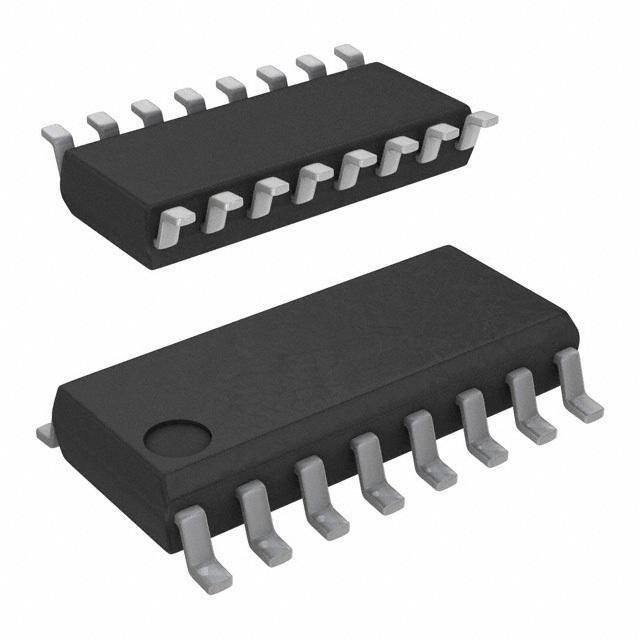
| 产品图片 |
|
| rohs | 符合RoHS无铅 / 符合限制有害物质指令(RoHS)规范要求 |
| 产品系列 | 电源管理 IC,开关控制器 ,Texas Instruments UCC2580D-1- |
| 数据手册 | |
| 产品型号 | UCC2580D-1 |
| PWM类型 | 电压模式 |
| 上升时间 | 40 ns |
| 下降时间 | 20 ns |
| 产品目录页面 | |
| 产品种类 | 开关控制器 |
| 倍增器 | 无 |
| 其它名称 | 296-11374-5 |
| 分频器 | 无 |
| 包装 | 管件 |
| 升压 | 是 |
| 单位重量 | 141.700 mg |
| 占空比 | 69% |
| 占空比-最大 | 69 % |
| 反向 | 无 |
| 反激式 | 是 |
| 同步管脚 | No |
| 商标 | Texas Instruments |
| 安装风格 | SMD/SMT |
| 封装 | Tube |
| 封装/外壳 | 16-SOIC(0.154",3.90mm 宽) |
| 封装/箱体 | SOIC-16 |
| 工作温度 | -40°C ~ 85°C |
| 工厂包装数量 | 40 |
| 开关频率 | 430 kHz |
| 拓扑结构 | Boost, Flyback, Forward |
| 最大工作温度 | + 85 C |
| 最小工作温度 | - 40 C |
| 标准包装 | 40 |
| 电压-电源 | 5.3 V ~ 8 V |
| 类型 | Voltage Mode PWM Controllers |
| 系列 | UCC2580-1 |
| 输出数 | 2 |
| 输出电流 | 1000 mA, 300 mA |
| 输出端数量 | 2 Output |
| 降压 | 无 |
| 隔离式 | 无 |
| 频率-最大值 | 1MHz |


- 商务部:美国ITC正式对集成电路等产品启动337调查
- 曝三星4nm工艺存在良率问题 高通将骁龙8 Gen1或转产台积电
- 太阳诱电将投资9.5亿元在常州建新厂生产MLCC 预计2023年完工
- 英特尔发布欧洲新工厂建设计划 深化IDM 2.0 战略
- 台积电先进制程称霸业界 有大客户加持明年业绩稳了
- 达到5530亿美元!SIA预计今年全球半导体销售额将创下新高
- 英特尔拟将自动驾驶子公司Mobileye上市 估值或超500亿美元
- 三星加码芯片和SET,合并消费电子和移动部门,撤换高东真等 CEO
- 三星电子宣布重大人事变动 还合并消费电子和移动部门
- 海关总署:前11个月进口集成电路产品价值2.52万亿元 增长14.8%


PDF Datasheet 数据手册内容提取
UCC1580-1,-2,-3,-4 UCC2580-1,-2,-3,-4 UCC3580-1,-2,-3,-4 Single Ended Active Clamp/Reset PWM FEATURES DESCRIPTION ProvidesAuxiliarySwitchActivation TheUCC3580familyofPWMcontrollersisdesignedtoimplementavariety ComplementarytoMainPower of active clamp/reset and synchronous rectifier switching converter topolo- SwitchDrive gies. While containing all the necessary functions for fixed frequency, high performance pulse width modulation, the additional feature of this design is Programmabledeadtime(Turn-on the inclusion of an auxiliary switch driver which complements the main Delay)BetweenActivationofEach Switch power switch, and with a programmable deadtime or delay between each transition. The active clamp/reset technique allows operation of single VoltageModeControlwith ended converters beyond 50% duty cycle while reducing voltage stresses FeedforwardOperation on the switches, and allows a greater flux swing for the power transformer. ProgrammableLimitsforBoth This approach also allows a reduction in switching losses by recovering en- TransformerVolt-SecondProduct ergy stored in parasitic elements such as leakage inductance and switch andPWMDutyCycle capacitance. HighCurrentGateDriverforBoth The oscillator is programmed with two resistors and a capacitor to set MainandAuxiliaryOutputs switching frequency and maximum duty cycle. A separate synchronized ramp provides a voltage feedforward pulse width modulation and a pro- MultipleProtectionFeatureswith grammed maximum volt-second limit. The generated clock from the oscilla- LatchedShutdownandSoftRestart torcontainsbothfrequencyandmaximumdutycycleinformation. LowSupplyCurrent(100(cid:1)AStartup, (continued) 1.5mAOperation) BLOCK DIAGRAM PinNumbersrefertoDIL-16andSOIC-16packages UDG-95069-2 SLUS292D-FEBRUARY1999-REVISED FEBRUARY 2007
UCC1580-1,-2,-3,-4 UCC2580-1,-2,-3,-4 UCC3580-1,-2,-3,-4 DESCRIPTION (cont.) The main gate drive output (OUT1) is controlled by the Undervoltage lockout monitors supply voltage (VDD), the pulse width modulator. The second output (OUT2) is in- precision reference (REF), input line voltage (LINE), and tended to activate an auxiliary switch during the off time the shutdown comparator (SHTDWN). If after any of of the main switch, except that between each transition these four have sensed a fault condition, recovery to full there is deadtime where both switches are off, pro- operation is initiated with a soft start. VDD thresholds, on grammed by a single external resistor. This design offers and off, are 15V and 8.5V for the -2 and -4 versions, 9V two options for OUT2, normal and inverted. In the -1 and and8.5Vforthe-1and-3versions. -2 versions, OUT2 is normal and can be used to drive The UCC1580-x is specified for operation over the mili- PMOSFETs.Inthe-3and -4versions,OUT2isinverted tary temperature range of -55°C to 125°C. The and can be used to drive NMOS FETs. In all versions, UCC2580-x is specified from -40°C to 85°C. The both the main and auxiliary switches are held off prior to UCC3580-x is specified from 0°C to 70°C. Package op- startup and when the PWM command goes to zero duty tionsinclude16-pinsurfacemountanddualin-line. cycle. During fault conditions, OUT1 is held off while OUT2 operates at maximum duty cycle with a guaran- teedofftimeequaltothesumofthetwodeadtimes. ABSOLUTE MAXIMUM RATINGS CONNECTION DIAGRAMS VDD...........................................16V I ..........................................25mA DIL-16,SOIC-16(TopView) VDD LINE,RAMP ........................ 0.3VtoVDD+1V J,N,orDPackages I ,I .....................................5mA LINE RAMP DELAY ........................................5.3V I ........................................ 5mA DELAY I (tpw<1 sandDutyCycle<10%)....... 0.6Ato1.2A OUT1 I (tpw<1 sandDutyCycle<10%)....... 0.4Ato0.4A OUT2 I ................................ 100mAto100mA CLK OSC1,OSC2,SS,SHTDWN,EAIN..... 0.3VtoREF+0.3V I .................................. 5mAto5mA EAOUT I ......................................... 30mA REF PGND.................................. 0.2Vto0.2V StorageTemperature.................. -65°Cto+150°C JunctionTemperature.................. -55°Cto+150°C LeadTemperature(Soldering,10sec.).............+300°C Allvoltagesarewithrespecttogroundunlessotherwisestated. Currents are positive into, negative out of the specified termi- nal. Consult Packaging Section of Databook for thermal limita- tionsandconsiderationsofpackages. ORDER INFORMATION 2
UCC1580-1,-2,-3,-4 UCC2580-1,-2,-3,-4 UCC3580-1,-2,-3,-4 ELECTRICAL CHARACTERISTICSUnlessotherwisestated,allspecificationsareoverthefulltemperaturerange,VDD= 12V,R1=18.2k(cid:1) ,R2=4.41k(cid:1) ,C =130pF,R3=100k(cid:1) ,C =0F,C =0F.T =0°Cto70°CfortheUCC3580, T OUT1 OUT2 A -40°Cto85°CfortheUCC2580, -55°Cto125°CfortheUCC1580,TA=TJ. PARAMETER TESTCONDITIONS MIN TYP MAX UNITS OscillatorSection Frequency 370 400 430 kHz CLKPulseWidth 650 750 850 ns CLKVOH ICLK= 3mA 4.3 4.7 V CLKVOL ICLK =3mA 0.3 0.5 V RampGeneratorSection RampVOL IRAMP=100(cid:1)A 50 100 mV FluxComparatorVth 3.16 3.33 3.50 V PulseWidthModulatorSection MinimumDutyCycle OUT1,EAOUT=VOL 0 % MaximumDutyCycle OUT1,EAIN=2.6V 63 66 69 % PWMComparatorOffset 0.1 0.4 0.9 V ErrorAmplifierSection EAIN EAOUT=EAIN 2.44 2.5 2.56 V IEAIN EAOUT=EAIN 150 400 nA EAOUT,VOL EAIN=2.6V,I =100(cid:1)A 0.3 0.5 V EAOUT EAOUT,VOH EAIN=2.4V,I = 100(cid:1)A 4 5 5.5 V EAOUT AVOL 70 80 dB GainBandwidthProduct f=100kHz(Note1) 2 6 MHz Softstart/ShutdownSection StartDutyCycle EAIN=2.4V 0 % SSVOL ISS=100(cid:1)A 100 350 mV SSRestartThreshold 400 550 mV ISS –20 –35 (cid:1)A SHTDWNVTH 0.4 0.5 0.6 V ISHTDWN 50 150 nA UndervoltageLockoutSection VDDOn UCC3580-2,-4 14 15 16 V UCC3580-1,-3 8 9 10 V VDDOff 7.5 8.5 9.5 V LINEOn 4.7 5 5.3 V LINEOff 4.2 4.5 4.8 V ILINE LINE=6V 50 150 nA SupplySection VDDClamp I =10mA 14 15 16 V VDD IVDDStart VDD<VDDOn 160 250 A IVDDOperating NoLoad 2.5 3.5 mA OutputDriversSection OUT1VSATHigh IOUT1= 50mA 0.4 1.0 V OUT1VSAT Low IOUT1=100mA 0.4 1.0 V OUT2VSAT High IOUT2= 30mA 0.4 1.0 V OUT2VSAT Low IOUT2 =30mA 0.4 1.0 V OUT1FallTime COUT1=1nF,RS=3(cid:1) 20 50 ns OUT1RiseTime COUT1 =1nF,RS=3(cid:1) 40 80 ns OUT2FallTime COUT2=300pF,RS=10(cid:1) 20 50 ns OUT2RiseTime C =300pF,R =10(cid:1) 20 40 ns OUT2 S 3
UCC1580-1,-2,-3,-4 UCC2580-1,-2,-3,-4 UCC3580-1,-2,-3,-4 ELECTRICAL CHARACTERISTICSUnlessotherwisestated,allspecificationsareoverthefulltemperaturerange,VDD= 12V,R1=18.2k(cid:1) ,R2=4.41k(cid:1) ,C =130pF,R3=100k(cid:1) ,C =0F,C =0F.T =0°Cto70°CfortheUCC3580, T OUT1 OUT2 A -40°Cto85°CfortheUCC2580, -55°Cto125°CfortheUCC1580,TA=TJ. PARAMETER TESTCONDITIONS MIN TYP MAX UNITS OutputDriversSection(cont.) Delay1OUT2toOUT1 R3=100k(cid:2),C =C =15pF 90 120 160 ns OUT1 OUT2 T =T =25°C 100 120 140 ns A J Delay2OUT1toOUT2 R3=100k(cid:2),C =C =15pF 110 170 250 ns OUT1 OUT2 T =T =25°C 140 170 200 ns A J ReferenceSection REF I =0 4.875 5 5.125 V REF LoadRegulation I =0mAto1mA 1 20 mV REF LineRegulation VDD=10Vto14V 1 20 mV Note1:Guaranteedbydesign.Not100%testedinproduction. PIN DESCRIPTIONS CLK: Oscillator clock output pin from a low impedance Maximum Duty Cycle for OUT1 is slightly less due to CMOS driver. CLK is high during guaranteed off time. Delay1whichisprogrammedbyR3. CLK can be used to synchronized up to five other OUT1: Gate drive output for the main switch capable of UCC3580PWMs. sourcingupto0.5Aandsinking1A. DELAY: A resistor from DELAY to GND programs the OUT2: Gate drive output for the auxiliary switch with nonoverlap delay between OUT1 and OUT2. The delay 0.3Adrivecurrentcapability. times,Delay1andDelay2,areshowninFigure1andare asfollows: PGND: Ground connection for the gate drivers. Connect PGNDtoGNDatasinglepointsothatnohighfrequency Delay1(cid:3)1.1pF(cid:4)R3 components of the output switching currents are in the Delay2 is designed to be larger than Delay1 by a ratio groundplaneonthecircuitboard. showninFigure2. RAMP: A resistor (R4) from RAMP to the input voltage EAIN: Inverting input to the error amplifier. The and a capacitor (CR) from RAMP to GND programs the noninvertinginputoftheerroramplifierisinternallysetto feedforward ramp signal. RAMP is discharged to GND 2.5V.EAINisusedforfeedbackandloopcompensation. when CLK is high and allowed to charge when CLK is low.RAMPisthelinefeedforwardsawtoothsignalforthe EAOUT: Output of the error amplifier and input to the PWM comparator. Assuming the input voltage is much PWM comparator. Loop compensation components greater than 3.3V, the ramp is very linear. A flux connectfromEAOUTtoEAIN. comparator compares the ramp signal to 3.3V to limit the GND:SignalGround. maximumallowablevolt-secondproduct: LINE:Hysteretic comparator input. Thresholds are 5.0V Volt-SecondProductClamp=3.3(cid:127)R4(cid:127)CR. and 4.5V. Used to sense input line voltage and turn off REF:Precision5.0Vreferencepin.REFcansupplyupto OUT1whenthelineislow. 5mAtoexternalcircuits.REFisoffuntilVDDexceeds9V OSC1 & OSC2: Oscillator programming pins. A resistor (–1 and –3 versions) or activates the 15V clamp (–2 and connects each pin to a timing capacitor. The resistor –4versions)andturnsoffagainwhenVDDdroopsbelow connected to OSC1 sets maximum on time. The resistor 8.5V.BypassREFtoGNDwitha1(cid:1)Fcapacitor. connected to OSC2 controls guaranteed off time. The SHTDWN: Comparator input to stop the chip. The combined total sets frequency with the timing capacitor. thresholdis0.5V.Whenthechipisstopped,OUT1islow Frequency and maximum duty cycle are approximately and OUT2 continues to oscillate with guaranteed off time givenby: equaltotwonon-overlapdelaytimes.OUT2continuesto 1.44 Frequency(cid:3) switch after SHTDWN is asserted until the voltage on (cid:5)R1(cid:7)R2(cid:6)(cid:4)(cid:5)CT(cid:7)27pF(cid:6) VDD falls below VCS (typically 4 V) in order to discharge theclampcapacitor. R1 Maximum DutyCycle(cid:3) R1(cid:7)R2 4
UCC1580-1,-2,-3,-4 UCC2580-1,-2,-3,-4 UCC3580-1,-2,-3,-4 PIN DESCRIPTIONS (cont.) SS: A capacitor from SS to ground programs the soft VDD: Chip power supply pin. VDD should be bypassed starttime.Duringsoftstart,EAOUTfollowstheamplitude to PGND. The –1 and –3 versions require VDD to ex- of SS’s slowly increasing waveform until regulation is ceed 9V to start and remain above 8.5V to continue run- achieved. ning. A shunt clamp from VDD to GND limits the supply voltage to 15V. The –2 and –4 versions do not start until APPLICATION INFORMATION UDG-95070-2 Note:Waveformsarenottoscale. Figure1.Outputtimerelationships. UVLOandStartup thisclampmustbeactivatedasanindicationofreaching the UVLO on threshold. The internal reference (REF) is For self biased off-line applications, -2 and -4 versions broughtupwhentheUVLOonthresholdiscrossed.The (UVLO on and off thresholds of 15V and 8.5V typical) startup logic ensures that LINE and REF are above and are recommended. For all other applications, -1 and -3 SHTDWN is below their respective thresholds before versions provide the lower on threshold of 9V. The IC re- quires a low startup current of only 160(cid:1)Awhen VDD is outputs are asserted. LINE input is useful for monitoring actual input voltage and shutting off the IC if it falls be- undertheUVLOthreshold,enablinguseofalargetrickle low a programmed value. A resistive divider should be charge resistor (with corresponding low power dissipa- used to connect the input voltage to the LINE input. This tion) from the input voltage. VDD has an internal clamp feature can protect the power supply from excessive at 15V which can sink up to 10mA. Measures should be currentsatlowlinevoltages. takennottoexceedthiscurrent.For-2and -4versions, 5
UCC1580-1,-2,-3,-4 UCC2580-1,-2,-3,-4 UCC3580-1,-2,-3,-4 APPLICATION INFORMATION (cont.) The soft start pin provides an effective means to start the IC in a controlled manner. An internal current of DelayTimes 20 Abegins charging a capacitor connected to SS once 1400 1.80 the startup conditions listed above have been met. The DelayRatio voltage on SS effectively controls maximum duty cycle 1200 1.70 on OUT1 during the charging period. OUT2 is also con- 1000 1.60 trolled during this period (see Figure 1). Negation of any o Delay2 Rati of the startup conditions causes SS to be immediately ns 800 1.50 ay1 discharged. Internal circuitry ensures full discharge of Delay 600 Delay1 1.40 Delay2/Del SprSov(itdoed0a.3llVth)ebsetfaorrteupaclloonwdinitgioncshaarrgeinaggatoinbmeegti.n again, 400 1.30 Oscillator 200 1.20 Simplified oscillator block diagram and waveforms are shown in Figure 3. OSC1 and OSC2 pins are used to 0 1.10 programthefrequencyandmaximumdutycycle.Capac- 0 100 200 300 400 500 600 700 800 900 1000 R3ProgrammingResistor(cid:1)k itorCTisalternatelychargedthroughR1anddischarged through R2 between levels of 1.67 V and 3.3 V. The charginganddischargingequationsforCTaregivenby Figure2.Delaytimes. (cid:9) (cid:12) VC(charge)=VREF •(cid:10)(cid:11)1(cid:8)23(cid:127)e-t(cid:15)1(cid:13)(cid:14) VC(discharge)= 2 (cid:4) V (cid:4)e-t(cid:15)2 3 REF where (cid:15) = R1 (cid:127) CT and (cid:15) = R2 (cid:127) CT. The charge time 1 2 anddischargetimearegivenby tCH=0.69(cid:127) R1(cid:127)C TandtDIS=0.69(cid:127)R2(cid:127)C T The CLK output is high during the discharge period. It blanks the output to limit the maximum duty cycle of OUT1. The frequency and maximum duty cycle are givenby 1.44 Frequency= (cid:5) (cid:6) (R1+R2)(cid:127) CT+ 27 pF R1 MaximumDutyCycle = R1+R2 Maximum Duty Cycle for OUT1 will be slightly less due toDelay1whichisprogrammedbyR3. VoltageFeedforwardandVolt-SecondClamp UCC3580 has a provision for input voltage feedforward. As shown in Figure 3, the ramp slope is made propor- tionaltoinputlinevoltagebyconvertingitintoacharging current for CR. This provides a first order cancellation of the effects of line voltage changes on converter perfor- mance. The maximum volt-second clamp is provided to protect against transient saturation of the transformer core.ItterminatestheOUT1pulsewhentheRAMPvolt- UDG-96016-1 ageexceeds3.3V.Ifthefeedforwardfeatureisnotused, Figure3.Oscillatorandrampcircuits. the ramp can be generated by tying R4 to REF. How- ever, the linearity of ramp suffers and in this case the maximumvolt-secondclampisnolongeravailable. 6
UCC1580-1,-2,-3,-4 UCC2580-1,-2,-3,-4 UCC3580-1,-2,-3,-4 APPLICATION INFORMATION (cont.) OutputConfigurations a single pin is used to program the delays between OUT1 and OUT2 on both sets of edges. Figure 1 shows The UCC3580 family of ICs is designed to provide con- therelationshipsbetweentheoutputs.Figure2givesthe trol functions for single ended active clamp circuits. For ratio between the two delays. During the transition from different implementations of the active clamp approach, main to auxiliary switch, the delay is not very critical for different drive waveforms for the two switches (main and ZVSturn-on.ForthefirsthalfofOUT1off-time,thebody auxiliary) are required. The -3 and -4 versions of the IC diode of the auxiliary switch conducts and OUT2 can be supply complementary non-overlapping waveforms turned on any time. The transition from auxiliary to main (OUT1 and OUT2) with programmable delay which can switch is more critical. Energy stored in the parasitic in- be used to drive the main and auxiliary switches. Most ductance(s) at the end of the OUT2 pulse is used to dis- active clamp configurations will require one of these out- charge the parasitic capacitance across the main switch puts to be transformer coupled to drive a floating switch duringthedelaytime.Thedelay(Delay1)shouldbeop- (e.g.Figure5).The-1and-2versionshavethephaseof timally programmed at 1/4 the resonant period deter- OUT2 inverted to give overlapping waveforms. This con- mined by parasitic capacitance and the resonant figuration is suitable for capacity coupled driving of a inductor (transformer leakage and/or magnetizing induc- ground referenced p-channel auxiliary switch with the tances, depending on the topology). However, depend- OUT2 drive while OUT1 is directly driving an n-channel ing on other circuit parasitics, the resonant behavior can mainswitch(e.g.Figure4). change,andinsomecases,ZVSturn-onmaynotbeob- The programmable delay can be judiciously used to get tainable. It can be shown that the optimum delay time is zero voltage turn-on of both the main and auxiliary independent of operating conditions for a specific circuit switches in the active clamp circuits. For the UCC3580, andshouldbedeterminedspecificallyforeachcircuit. UDG-95071-2 Figure4.Activeclampforwardconverter. 7
UCC1580-1,-2,-3,-4 UCC2580-1,-2,-3,-4 UCC3580-1,-2,-3,-4 APPLICATION INFORMATION (cont.) UDG-96017-1 Figure5.Off-lineactiveclampflybackconverter. The use of active reset in a flyback power converter topology may be covered by U.S. Patent No. 5,402,329 owned by Technical Witts,Inc.,andforwhichUnitrodeoffersusersapaiduplicenseforapplicationoftheUCC1580productfamily. 8
UCC1580-1,-2,-3,-4 UCC2580-1,-2,-3,-4 UCC3580-1,-2,-3,-4 APPLICATION INFORMATION (cont.) UDG-96018-1 Figure6.UCC3580usedinasynchronousrectifierapplication. REVISION DATE COMMENT SLUS292B MAY2005 UpdatedOSCfrequencyandmaximumdutycycle,CTchargeanddischarge equations. UpdatedSHTDWNpindescription. UpdatedtypicalCTvalueusedformeasurementsinelectricalcharacteristics table. SLUS292C MAY2005 RemovedQpackagefromdatasheet. 9
PACKAGE OPTION ADDENDUM www.ti.com 6-Feb-2020 PACKAGING INFORMATION Orderable Device Status Package Type Package Pins Package Eco Plan Lead/Ball Finish MSL Peak Temp Op Temp (°C) Device Marking Samples (1) Drawing Qty (2) (6) (3) (4/5) HPA00033DTR ACTIVE SOIC D 16 2500 Green (RoHS NIPDAU Level-1-260C-UNLIM 0 to 70 UCC3580D-1 & no Sb/Br) HPA00034DTR ACTIVE SOIC D 16 2500 Green (RoHS NIPDAU Level-1-260C-UNLIM 0 to 70 UCC3580D-2 & no Sb/Br) HPA00036DTR ACTIVE SOIC D 16 2500 Green (RoHS NIPDAU Level-1-260C-UNLIM 0 to 70 UCC3580D-4 & no Sb/Br) HPA00706DTR-2 ACTIVE SOIC D 16 2500 Green (RoHS NIPDAU Level-1-260C-UNLIM -40 to 85 UCC2580D-2 & no Sb/Br) UCC2580D-1 ACTIVE SOIC D 16 40 Green (RoHS NIPDAU Level-1-260C-UNLIM -40 to 85 UCC2580D-1 & no Sb/Br) UCC2580D-2 ACTIVE SOIC D 16 40 Green (RoHS NIPDAU Level-1-260C-UNLIM -40 to 85 UCC2580D-2 & no Sb/Br) UCC2580D-3 ACTIVE SOIC D 16 40 Green (RoHS NIPDAU Level-1-260C-UNLIM -40 to 85 UCC2580D-3 & no Sb/Br) UCC2580D-3G4 ACTIVE SOIC D 16 40 Green (RoHS NIPDAU Level-1-260C-UNLIM -40 to 85 UCC2580D-3 & no Sb/Br) UCC2580D-4 ACTIVE SOIC D 16 40 Green (RoHS NIPDAU Level-1-260C-UNLIM -40 to 85 UCC2580D-4 & no Sb/Br) UCC2580DTR-1 ACTIVE SOIC D 16 2500 Green (RoHS NIPDAU Level-1-260C-UNLIM -40 to 85 UCC2580D-1 & no Sb/Br) UCC2580DTR-2 ACTIVE SOIC D 16 2500 Green (RoHS NIPDAU Level-1-260C-UNLIM -40 to 85 UCC2580D-2 & no Sb/Br) UCC2580DTR-3 ACTIVE SOIC D 16 2500 Green (RoHS NIPDAU Level-1-260C-UNLIM -40 to 85 UCC2580D-3 & no Sb/Br) UCC2580DTR-4 ACTIVE SOIC D 16 2500 Green (RoHS NIPDAU Level-1-260C-UNLIM -40 to 85 UCC2580D-4 & no Sb/Br) UCC3580D-1 ACTIVE SOIC D 16 40 Green (RoHS NIPDAU Level-1-260C-UNLIM 0 to 70 UCC3580D-1 & no Sb/Br) UCC3580D-2 ACTIVE SOIC D 16 40 Green (RoHS NIPDAU Level-1-260C-UNLIM 0 to 70 UCC3580D-2 & no Sb/Br) UCC3580D-2G4 ACTIVE SOIC D 16 40 Green (RoHS NIPDAU Level-1-260C-UNLIM 0 to 70 UCC3580D-2 & no Sb/Br) UCC3580D-3 ACTIVE SOIC D 16 40 Green (RoHS NIPDAU Level-1-260C-UNLIM 0 to 70 UCC3580D-3 & no Sb/Br) Addendum-Page 1
PACKAGE OPTION ADDENDUM www.ti.com 6-Feb-2020 Orderable Device Status Package Type Package Pins Package Eco Plan Lead/Ball Finish MSL Peak Temp Op Temp (°C) Device Marking Samples (1) Drawing Qty (2) (6) (3) (4/5) UCC3580D-4 ACTIVE SOIC D 16 40 Green (RoHS NIPDAU Level-1-260C-UNLIM 0 to 70 UCC3580D-4 & no Sb/Br) UCC3580DTR-1 ACTIVE SOIC D 16 2500 Green (RoHS NIPDAU Level-1-260C-UNLIM 0 to 70 UCC3580D-1 & no Sb/Br) UCC3580DTR-2 ACTIVE SOIC D 16 2500 Green (RoHS NIPDAU Level-1-260C-UNLIM 0 to 70 UCC3580D-2 & no Sb/Br) UCC3580DTR-3 ACTIVE SOIC D 16 2500 Green (RoHS NIPDAU Level-1-260C-UNLIM 0 to 70 UCC3580D-3 & no Sb/Br) UCC3580DTR-4 ACTIVE SOIC D 16 2500 Green (RoHS NIPDAU Level-1-260C-UNLIM 0 to 70 UCC3580D-4 & no Sb/Br) (1) The marketing status values are defined as follows: ACTIVE: Product device recommended for new designs. LIFEBUY: TI has announced that the device will be discontinued, and a lifetime-buy period is in effect. NRND: Not recommended for new designs. Device is in production to support existing customers, but TI does not recommend using this part in a new design. PREVIEW: Device has been announced but is not in production. Samples may or may not be available. OBSOLETE: TI has discontinued the production of the device. (2) RoHS: TI defines "RoHS" to mean semiconductor products that are compliant with the current EU RoHS requirements for all 10 RoHS substances, including the requirement that RoHS substance do not exceed 0.1% by weight in homogeneous materials. Where designed to be soldered at high temperatures, "RoHS" products are suitable for use in specified lead-free processes. TI may reference these types of products as "Pb-Free". RoHS Exempt: TI defines "RoHS Exempt" to mean products that contain lead but are compliant with EU RoHS pursuant to a specific EU RoHS exemption. Green: TI defines "Green" to mean the content of Chlorine (Cl) and Bromine (Br) based flame retardants meet JS709B low halogen requirements of <=1000ppm threshold. Antimony trioxide based flame retardants must also meet the <=1000ppm threshold requirement. (3) MSL, Peak Temp. - The Moisture Sensitivity Level rating according to the JEDEC industry standard classifications, and peak solder temperature. (4) There may be additional marking, which relates to the logo, the lot trace code information, or the environmental category on the device. (5) Multiple Device Markings will be inside parentheses. Only one Device Marking contained in parentheses and separated by a "~" will appear on a device. If a line is indented then it is a continuation of the previous line and the two combined represent the entire Device Marking for that device. (6) Lead/Ball Finish - Orderable Devices may have multiple material finish options. Finish options are separated by a vertical ruled line. Lead/Ball Finish values may wrap to two lines if the finish value exceeds the maximum column width. Important Information and Disclaimer:The information provided on this page represents TI's knowledge and belief as of the date that it is provided. TI bases its knowledge and belief on information provided by third parties, and makes no representation or warranty as to the accuracy of such information. Efforts are underway to better integrate information from third parties. TI has taken and Addendum-Page 2
PACKAGE OPTION ADDENDUM www.ti.com 6-Feb-2020 continues to take reasonable steps to provide representative and accurate information but may not have conducted destructive testing or chemical analysis on incoming materials and chemicals. TI and TI suppliers consider certain information to be proprietary, and thus CAS numbers and other limited information may not be available for release. In no event shall TI's liability arising out of such information exceed the total purchase price of the TI part(s) at issue in this document sold by TI to Customer on an annual basis. Addendum-Page 3
PACKAGE MATERIALS INFORMATION www.ti.com 11-Feb-2018 TAPE AND REEL INFORMATION *Alldimensionsarenominal Device Package Package Pins SPQ Reel Reel A0 B0 K0 P1 W Pin1 Type Drawing Diameter Width (mm) (mm) (mm) (mm) (mm) Quadrant (mm) W1(mm) UCC2580DTR-1 SOIC D 16 2500 330.0 16.4 6.5 10.3 2.1 8.0 16.0 Q1 UCC2580DTR-2 SOIC D 16 2500 330.0 16.4 6.5 10.3 2.1 8.0 16.0 Q1 UCC2580DTR-3 SOIC D 16 2500 330.0 16.4 6.5 10.3 2.1 8.0 16.0 Q1 UCC2580DTR-4 SOIC D 16 2500 330.0 16.4 6.5 10.3 2.1 8.0 16.0 Q1 UCC3580DTR-1 SOIC D 16 2500 330.0 16.4 6.5 10.3 2.1 8.0 16.0 Q1 UCC3580DTR-2 SOIC D 16 2500 330.0 16.4 6.5 10.3 2.1 8.0 16.0 Q1 UCC3580DTR-3 SOIC D 16 2500 330.0 16.4 6.5 10.3 2.1 8.0 16.0 Q1 UCC3580DTR-4 SOIC D 16 2500 330.0 16.4 6.5 10.3 2.1 8.0 16.0 Q1 PackMaterials-Page1
PACKAGE MATERIALS INFORMATION www.ti.com 11-Feb-2018 *Alldimensionsarenominal Device PackageType PackageDrawing Pins SPQ Length(mm) Width(mm) Height(mm) UCC2580DTR-1 SOIC D 16 2500 333.2 345.9 28.6 UCC2580DTR-2 SOIC D 16 2500 333.2 345.9 28.6 UCC2580DTR-3 SOIC D 16 2500 333.2 345.9 28.6 UCC2580DTR-4 SOIC D 16 2500 333.2 345.9 28.6 UCC3580DTR-1 SOIC D 16 2500 333.2 345.9 28.6 UCC3580DTR-2 SOIC D 16 2500 333.2 345.9 28.6 UCC3580DTR-3 SOIC D 16 2500 333.2 345.9 28.6 UCC3580DTR-4 SOIC D 16 2500 333.2 345.9 28.6 PackMaterials-Page2
None
None
IMPORTANTNOTICEANDDISCLAIMER TI PROVIDES TECHNICAL AND RELIABILITY DATA (INCLUDING DATASHEETS), DESIGN RESOURCES (INCLUDING REFERENCE DESIGNS), APPLICATION OR OTHER DESIGN ADVICE, WEB TOOLS, SAFETY INFORMATION, AND OTHER RESOURCES “AS IS” AND WITH ALL FAULTS, AND DISCLAIMS ALL WARRANTIES, EXPRESS AND IMPLIED, INCLUDING WITHOUT LIMITATION ANY IMPLIED WARRANTIES OF MERCHANTABILITY, FITNESS FOR A PARTICULAR PURPOSE OR NON-INFRINGEMENT OF THIRD PARTY INTELLECTUAL PROPERTY RIGHTS. These resources are intended for skilled developers designing with TI products. You are solely responsible for (1) selecting the appropriate TI products for your application, (2) designing, validating and testing your application, and (3) ensuring your application meets applicable standards, and any other safety, security, or other requirements. These resources are subject to change without notice. TI grants you permission to use these resources only for development of an application that uses the TI products described in the resource. Other reproduction and display of these resources is prohibited. No license is granted to any other TI intellectual property right or to any third party intellectual property right. TI disclaims responsibility for, and you will fully indemnify TI and its representatives against, any claims, damages, costs, losses, and liabilities arising out of your use of these resources. TI’s products are provided subject to TI’s Terms of Sale (www.ti.com/legal/termsofsale.html) or other applicable terms available either on ti.com or provided in conjunction with such TI products. TI’s provision of these resources does not expand or otherwise alter TI’s applicable warranties or warranty disclaimers for TI products. Mailing Address: Texas Instruments, Post Office Box 655303, Dallas, Texas 75265 Copyright © 2020, Texas Instruments Incorporated