ICGOO在线商城 > 集成电路(IC) > PMIC - 电源管理 - 专用 > UC3907N

 Datasheet下载
- 型号: UC3907N
- 制造商: Texas Instruments
- 库位|库存: xxxx|xxxx
- 要求:
| 数量阶梯 | 香港交货 | 国内含税 |
| +xxxx | $xxxx | ¥xxxx |
查看当月历史价格
查看今年历史价格
UC3907N产品简介:
ICGOO电子元器件商城为您提供UC3907N由Texas Instruments设计生产,在icgoo商城现货销售,并且可以通过原厂、代理商等渠道进行代购。 UC3907N价格参考¥21.88-¥40.85。Texas InstrumentsUC3907N封装/规格:PMIC - 电源管理 - 专用, Load Share Controller PMIC 16-PDIP。您可以下载UC3907N参考资料、Datasheet数据手册功能说明书,资料中有UC3907N 详细功能的应用电路图电压和使用方法及教程。
Texas Instruments(德州仪器)的UC3907N是一款专用电源管理集成电路(PMIC),主要用于电池充电和保护应用。以下是其主要应用场景:

1. 便携式电子设备:
   UC3907N广泛应用于便携式电子设备,如笔记本电脑、平板电脑、智能手机、便携式音频/视频设备等。它能够为这些设备中的可充电电池提供高效的充电管理和保护功能。

2. 电池充电管理:
   该芯片支持对镍氢(NiMH)和镍镉(NiCd)电池进行恒流/恒压充电管理。它可以通过监测电池电压、电流和温度来确保安全和高效的充电过程。

3. 多节电池组保护:
   UC3907N可以用于多节电池组的保护系统中,防止过充、过放、过流和短路等情况发生,从而延长电池寿命并提高安全性。

4. 工业设备:
   在一些需要可靠电源管理的工业设备中,例如手持扫描仪、测试仪器和便携式医疗设备,UC3907N能够提供稳定的电源解决方案。

5. 通信设备:
   该芯片适用于通信领域的便携式设备,如无线对讲机、路由器和调制解调器,确保设备在移动状态下的持续供电。

6. 汽车电子:
   虽然UC3907N主要针对消费类电子产品,但在某些汽车电子应用中,例如便携式导航设备或车载娱乐系统,它也可以作为电池管理方案的一部分。

总结来说,UC3907N是一款高度集成的电源管理芯片,专为需要高效电池充电和保护的场景设计,能够在多种便携式设备中发挥重要作用。
| 参数 | 数值 |
| 产品目录 | 集成电路 (IC)半导体 |
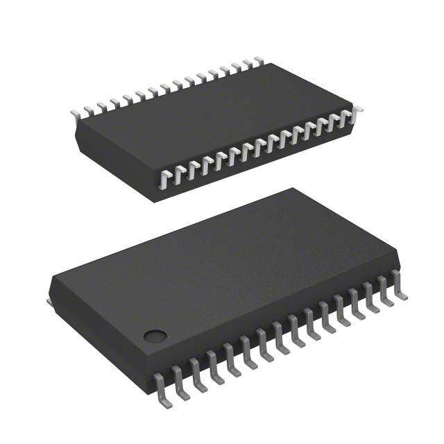
| 描述 | IC LOAD SHARE CONTROLLER 16-DIP专业电源管理 LOAD SHARE CONTROLLER |
| 产品分类 | |
| 品牌 | Texas Instruments |
| 产品手册 | |
| 产品图片 |
|
| rohs | 符合RoHS无铅 / 符合限制有害物质指令(RoHS)规范要求 |
| 产品系列 | 电源管理 IC,专业电源管理,Texas Instruments UC3907N- |
| 数据手册 | |
| 产品型号 | UC3907N |
| 产品目录页面 | |
| 产品种类 | 专业电源管理 |
| 供应商器件封装 | 16-PDIP |
| 其它名称 | 296-11344-5 |
| 包装 | 管件 |
| 单位重量 | 1.054 g |
| 商标 | Texas Instruments |
| 安装类型 | 通孔 |
| 安装风格 | Through Hole |
| 封装 | Tube |
| 封装/外壳 | 16-DIP(0.300",7.62mm) |
| 封装/箱体 | PDIP-16 |
| 工作温度 | 0°C ~ 70°C |
| 工作温度范围 | 0 C to + 70 C |
| 工厂包装数量 | 25 |
| 应用 | 负荷分载控制器 |
| 标准包装 | 25 |
| 电压-电源 | 4.5 V ~ 36 V |
| 电流-电源 | 6mA |
| 电源电压 | 4.5 V to 36 V |
| 类型 | Load Share Controllers |
| 系列 | UC3907 |
| 输入电压范围 | 4.5 V to 36 V |
| 输入电流 | 6 mA |
| 输出电压范围 | 1.955 V to 2.045 V |
| 输出电流 | 600 uA |
| 配用 | /product-detail/zh/UCC39002EVM/296-19045-ND/863866 |


- 商务部:美国ITC正式对集成电路等产品启动337调查
- 曝三星4nm工艺存在良率问题 高通将骁龙8 Gen1或转产台积电
- 太阳诱电将投资9.5亿元在常州建新厂生产MLCC 预计2023年完工
- 英特尔发布欧洲新工厂建设计划 深化IDM 2.0 战略
- 台积电先进制程称霸业界 有大客户加持明年业绩稳了
- 达到5530亿美元!SIA预计今年全球半导体销售额将创下新高
- 英特尔拟将自动驾驶子公司Mobileye上市 估值或超500亿美元
- 三星加码芯片和SET,合并消费电子和移动部门,撤换高东真等 CEO
- 三星电子宣布重大人事变动 还合并消费电子和移动部门
- 海关总署:前11个月进口集成电路产品价值2.52万亿元 增长14.8%


PDF Datasheet 数据手册内容提取
(cid:21) (cid:1)(cid:2)(cid:3)(cid:4)(cid:5)(cid:6)(cid:7) (cid:1)(cid:2)(cid:9)(cid:4)(cid:5)(cid:6)(cid:7) (cid:1)(cid:2)(cid:10)(cid:4)(cid:5)(cid:6) (cid:11)(cid:12)(cid:13)(cid:14) (cid:15)(cid:16)(cid:13)(cid:17)(cid:18) (cid:2)(cid:12)(cid:19)(cid:20)(cid:17)(cid:12)(cid:11)(cid:11)(cid:18)(cid:17) SLUS165C – MARCH 1999 - REVISED JANUARY 2002 FEATURES SOIC-16 DW PACKAGE (cid:1) (TOP VIEW) Fully Differential High Impedance Voltage Sensing C/S OUT 1 16 STATUS INDICATE (cid:1) Accurate Current Amplifier for Precise C/S (+) 2 15 CURRENT SHARE BUS Current Sharing C/S (–) 3 14 ADJ OUT (cid:1) (–) SENSE 4 13 ADJ INPUT Opto Coupler Driving Capability (cid:1) 1.25% Trimmed Reference S POWER RETURN 5 12 COMP U ARTIFICIAL GND 6 11 (+) SENSE (cid:1) B Master Status Indication E E VREF 7 10 VCC (cid:1) 4.5-V to 35-V Operation AT AR ISET 8 9 OPTO DRIVE C H DI S PLCC-20, LCC-20, N T Q O(RTO LP P VAICEKWA)GE C/S (+) C/S OUT N/C STATUS I CURREN DIL-16( TJO oPr NV IPEAWC)KAGE 3 2 1 20 19 C/S OUT 1 16 STATUS INDICATE C/S (–) 4 18 ADJ OUT C/S (+) 2 15 CURRENT SHARE BUS (–) SENSE 5 17 ADJ INPUT C/S (–) 3 14 ADJ OUT N/C 6 16 N/C (–) SENSE 4 13 ADJ INPUT POWER RETURN 7 15 COMP POWER RETURN 5 12 COMP ARTIFICIAL GND 8 14 ARTIFICIAL GND 6 11 (+) SENSE (+) SENSE 9 10 11 12 13 VREF 7 10 VCC F T C E C ISET 8 9 OPTO DRIVE RE SE N/ RIV VC V I D O DESCRIPTION T P O The UCx907 family of load share controller ICs provides all the necessary features to allow multiple-independent-power modules to be paralleled such that each module supplies only its proportionate share to total-load current. This sharing is accomplished by controlling each module’s power stage with a command generated from a voltage-feedback amplifier whose reference can be independently adjusted in response to a common-share-bus voltage. By monitoring the current from each module, the current share bus circuitry determines which paralleled module would normally have the highest output current and, with the designation of this unit as the master, adjusts all the other modules to increase their output current to within 2.5% of that of the master. The current share bus signal interconnecting all the paralleled modules is a low-impedance, noise-insensitive line which will not interfere with allowing each module to act independently should the bus become open or shorted to ground. The UC3907 controller will reside on the output side of each power module and its overall function is to supply a voltage feedback loop. The specific architecture of the power stage is unimportant. Either switching or linear designs may be utilized and the control signal may be either directly coupled or isolated though the use of an optocoupler or other isolated medium. Other features of the UC3907 include 1.25% accurate reference: a low-loss, fixed-gain current-sense amplifier, a fully differential, high-impedance voltage sensing capability, and a status indicator to designate which module is performing as master. Please be aware that an important notice concerning availability, standard warranty, and use in critical applications of TexasInstruments semiconductor products and disclaimers thereto appears at the end of this data sheet. (cid:22)(cid:17)(cid:12)(cid:14)(cid:1)(cid:2)(cid:20)(cid:23)(cid:12)(cid:19) (cid:14)(cid:13)(cid:20)(cid:13) (cid:24)(cid:25)(cid:26)(cid:27)(cid:28)(cid:29)(cid:30)(cid:31)(cid:24)(cid:27)(cid:25) (cid:24) !"(cid:28)(cid:28)#(cid:25)(cid:31) (cid:30) (cid:27)(cid:26) $"%&(cid:24)!(cid:30)(cid:31)(cid:24)(cid:27)(cid:25) ’(cid:30)(cid:31)#( Copyright 2000, Texas Instruments Incorporated (cid:22)(cid:28)(cid:27)’"!(cid:31) !(cid:27)(cid:25)(cid:26)(cid:27)(cid:28)(cid:29) (cid:31)(cid:27) $#!(cid:24)(cid:26)(cid:24)!(cid:30)(cid:31)(cid:24)(cid:27)(cid:25) $#(cid:28) (cid:31))# (cid:31)#(cid:28)(cid:29) (cid:27)(cid:26) (cid:20)#*(cid:30) (cid:23)(cid:25) (cid:31)(cid:28)"(cid:29)#(cid:25)(cid:31) (cid:31)(cid:30)(cid:25)’(cid:30)(cid:28)’ +(cid:30)(cid:28)(cid:28)(cid:30)(cid:25)(cid:31),( (cid:22)(cid:28)(cid:27)’"!(cid:31)(cid:24)(cid:27)(cid:25) $(cid:28)(cid:27)!# (cid:24)(cid:25)- ’(cid:27)# (cid:25)(cid:27)(cid:31) (cid:25)#!# (cid:30)(cid:28)(cid:24)&, (cid:24)(cid:25)!&"’# (cid:31)# (cid:31)(cid:24)(cid:25)- (cid:27)(cid:26) (cid:30)&& $(cid:30)(cid:28)(cid:30)(cid:29)#(cid:31)#(cid:28) ( www.ti.com 1
(cid:1)(cid:2)(cid:3)(cid:4)(cid:5)(cid:6)(cid:7) (cid:1)(cid:2)(cid:9)(cid:4)(cid:5)(cid:6)(cid:7) (cid:1)(cid:2)(cid:10)(cid:4)(cid:5)(cid:6) (cid:21) (cid:11)(cid:12)(cid:13)(cid:14) (cid:15)(cid:16)(cid:13)(cid:17)(cid:18) (cid:2)(cid:12)(cid:19)(cid:20)(cid:17)(cid:12)(cid:11)(cid:11)(cid:18)(cid:17) SLUS165C – MARCH 1999 - REVISED JANUARY 2002 block diagram VOLTAGE ERROR AMPLIFIER (+) SENSE 11 – 12 COMP VCC (4.5 V TO 35 V) 10 + VCC 1.75 V DRIVE 0.25 V 1.0 V AMPLIFIER 9 OPTO DRIVE + + + GROUND VREF –DRV AMPLIFIER 1.75 V 1 kΩ – 20 kΩ 50 kΩ GND (–) SENSE 4 + 8 ISET POWER RTN 5 14 ADJ OUT ADJUST ARTIFICIAL GND 6 AMPLIFIER 50 mV + 17.5 kΩ – 13 ADJ INPUT VREF 7 ADJ + C/S OUT 1 40 kΩ BUFFER CURRENT SENSE AMPLIFIER 2 kΩ AMPLIFIER C/S (–) 3 100 – – 15 CURRENT SHARE BUS 2 kΩ + C/S (+) 2 + 10 kΩ 16 STATUS INDICATE 40 kΩ absolute maximum ratings over operating free-air temperature (unless otherwise noted)† Supply voltage . . . . . . . . . . . . . . . . . . . . . . . . . . . . . . . . . . . . . . . . . . . . . . . . . . . . . . . . . . . . . . . . . . . . . . . . . . . . . 35 V Opto out voltage . . . . . . . . . . . . . . . . . . . . . . . . . . . . . . . . . . . . . . . . . . . . . . . . . . . . . . . . . . . . . . . . . . . . . . . . . . . 35 V Opto out current. . . . . . . . . . . . . . . . . . . . . . . . . . . . . . . . . . . . . . . . . . . . . . . . . . . . . . . . . . . . . . . . . . . . . . . . . . . 20 mA Status indicate sink current . . . . . . . . . . . . . . . . . . . . . . . . . . . . . . . . . . . . . . . . . . . . . . . . . . . . . . . . . . . . . . . . . 20 mA C/S input voltage . . . . . . . . . . . . . . . . . . . . . . . . . . . . . . . . . . . . . . . . . . . . . . . . . . . . . . . . . . . . . . . . . . . . . . . . . . . 35 V Share bus voltage . . . . . . . . . . . . . . . . . . . . . . . . . . . . . . . . . . . . . . . . . . . . . . . . . . . . . . . . . . . . . . . . . . –0.3 V to 35 V Other analog inputs and outputs (zener clamped) maximum forced voltage . . . . . . . . . . . . . . . . –0.3 V to10 V Other analog inputs and outputs (zener clamped) maximum forced current . . . . . . . . . . . . . . . . . . . . . ±10 mA Ground amp sink current . . . . . . . . . . . . . . . . . . . . . . . . . . . . . . . . . . . . . . . . . . . . . . . . . . . . . . . . . . . . . . . . . . . 50 mA Pins 1, 9, 12, 15 sink current . . . . . . . . . . . . . . . . . . . . . . . . . . . . . . . . . . . . . . . . . . . . . . . . . . . . . . . . . . . . . . . . 20 mA Storage temperature range, T . . . . . . . . . . . . . . . . . . . . . . . . . . . . . . . . . . . . . . . . . . . . . . . . . . . –65°C to 150°C stg Junction temperature, T . . . . . . . . . . . . . . . . . . . . . . . . . . . . . . . . . . . . . . . . . . . . . . . . . . . . . . . . . . –55°C to 150°C J Lead temperature (solder 10 seconds) . . . . . . . . . . . . . . . . . . . . . . . . . . . . . . . . . . . . . . . . . . . . . . . . . . . . . . . 300°C †Pin Nos. refer to 16 Pin DIL Package. ‡Currents are positive into, negative out of the specified terminal. Consult packaging section of databook for thermal limitations and considerations of package. 2 www.ti.com
(cid:21) (cid:1)(cid:2)(cid:3)(cid:4)(cid:5)(cid:6)(cid:7) (cid:1)(cid:2)(cid:9)(cid:4)(cid:5)(cid:6)(cid:7) (cid:1)(cid:2)(cid:10)(cid:4)(cid:5)(cid:6) (cid:11)(cid:12)(cid:13)(cid:14) (cid:15)(cid:16)(cid:13)(cid:17)(cid:18) (cid:2)(cid:12)(cid:19)(cid:20)(cid:17)(cid:12)(cid:11)(cid:11)(cid:18)(cid:17) SLUS165C – MARCH 1999 - REVISED JANUARY 2002 electrical characteristics, these specifications apply for T = –55°C to 125°C for UC1907, –40°C to A 85°C for UC2907, and 0°C to 70°C for UC3907, V = 15 V, T = T (unless otherwise stated ) IN A J PARAMETER TEST CONDITIONS MIN TYP MAX UNITS Voltage Amp Section COMP = 1 V, TA = 25°C 1.975 2.000 2.025 V IInnpputt voollttaaggee COMP = 1 V, over temp 1.960 2.000 2.040 V Line regulation VIN = 4.5 V to 35 V 15 mV Load regulation IL reference = 0.0 mA to –10 mA 10 mV Long term stability TA = 125°C, 1000hrs See Note 2 5 25 mV Total output variation Line, load, temp 1.960 2.040 Input adjust range ADJ OUT from max high to max low 85 100 115 mV Input bias current –1 µA Open loop gain COMP = 0.75 V to 1.5 V 65 dB Unity gain bandwidth TA = 25°C See Note 2 700 kHz Output sink current (+) SENSE = 2.2 V, COMP = 1 V 6 15 mA Output source current (+) SENSE = 1.8 V, COMP = 1 V 400 600 µA VOUT high (+) SENSE = 1.8 V, IL = –400 µΑ 1.85 2 V VOUT low (+) SENSE = 2.2 V, IL = 1 mA 0.15 0.40 V Reference Section TA = 25°C 1.970 2.000 2.030 V OOuttpputt voollttaaggee Over operating temp 1.955 2.000 2.045 V Short circuit current VREF = 0.0 V –15 –30 –60 mA Ground Amp Section Output voltage 200 250 300 mV Common mode variation (–) SENSE from 0.0 V to 2 V 5 mV IL = 0.0 mA to 20 mA, TA = 25°C 10 mV LLooaadd rreeggullaattiioonn IL = 0.0 mA to 20 mA, over temp 15 mV Adjust Amp Section Input offset voltage ADJ OUT = 1.5 V, VCM = 0.0 V 40 50 60 mV Input bias current –2 µA Open loop gain 1.5 V ≤ ADJ OUT≤ 2.25 V 65 dB Unity gain bandwidth TA = 25°C, COUT =1 µF See Note 2 500 Hz Transconductance IOUT = –10 µA to 10 µA, VOUT = 1.5 V 1.7 3 4.5 ms Output sink current VID = 0.0 V, ADJ OUT = 1.5 V 55 135 225 µA Output source current VID = 250 mV, ADJ OUT = 1.5 V 110 200 350 µA VOUT high VID = 250 mV, IOUT = – 50 mA 2.20 2.70 2.90 V VOUT low VID = 0.0 V, IOUT = 50 mA 0.75 1.15 V Common mode rejection ratio VCM = 0.0 to 10 V 70 dB Output gain to V/A V∆(O+U) ST EANDSJE O/ U∆ATD =J 1 O.5U VT to 2 V, 50 57 64 mV/V NOTE 1: Unless otherwise specified all voltages are with respect to (–) SENSE. Currents are positive into, negative out of the specified terminal. NOTE 2: Ensured by design. Not production tested. www.ti.com 3
(cid:1)(cid:2)(cid:3)(cid:4)(cid:5)(cid:6)(cid:7) (cid:1)(cid:2)(cid:9)(cid:4)(cid:5)(cid:6)(cid:7) (cid:1)(cid:2)(cid:10)(cid:4)(cid:5)(cid:6) (cid:21) (cid:11)(cid:12)(cid:13)(cid:14) (cid:15)(cid:16)(cid:13)(cid:17)(cid:18) (cid:2)(cid:12)(cid:19)(cid:20)(cid:17)(cid:12)(cid:11)(cid:11)(cid:18)(cid:17) SLUS165C – MARCH 1999 - REVISED JANUARY 2002 electrical characteristics, these specifications apply for T = –55°C to 125°C for UC1907, –40°C to A 85°C for UC2907, and 0°C to 70°C for UC3907, V = 15 V, T = T (unless otherwise stated ) IN A J PARAMETER TEST CONDITIONS MIN TYP MAX UNITS Current Amp Section Gain VCM = 0.0 V, VID = 50 mV to 100 mV 19.2 19.6 20.1 V/V VC/S (+) = VC/S (–) = 0.0 V, TA = 25°C 210 250 290 mV OOuttpputt voollttaaggee VC/S (+) = VC/S (–) = 0.0 V, over temp 180 250 330 mV Input offset change with common mode VCM = 0 V to 13 V 600 µV/V input VOUT high VID = 1 V 10 14.5 V VOUT low VID = – 1 V, IL = 1 mA 350 450 mV Power supply rejection ratio VIN = 4.5 V to 35 V, VCM = 0.0 V 60 dB Slew rate 0.4 V/µs Drive Amp Section RSET = 500 Ω to Artificial GND, Opto Drive = 15 V Voltage gain COMP = 0.5 V to 1 V 2.3 2.5 2.6 V/V ISET VOUT high (+) SENSE = 2.2 V 3.8 4.1 4.4 V ISET VOUT low (+) SENSE = 1.8 V 270 300 mV Opto out voltage range 4 35 V Zero current input threshold 1.55 1.65 1.75 V Buffer Amp Section Input offset voltage Input = 1 V 5 mV Output off impedance Input = 1 V, output = 1.5 V to 2 V 5 10 20 kΩ Output source current Input = 1 V, output = 0.5 V 6 15 mA Common mode rejection ratio VCM = 0.3 V to 10 V 70 dB Power supply rejection ratio VIN = 4.5 V to 35 V 70 dB Under Voltage Lockout Section Startup threshold 3.7 4.4 V Threshold hysteresis 200 mV Status Indicate Section VOUT low ADJ OUT = current share bus 0.2 0.5 V Output leakage ADJ OUT = 1 V, VOUT = 35 V 0.1 5 µA Total Stand by Current Section Startup current VIN = UVLO – 0.2 V 3 5 mA Operating current VIN = 35 V 6 10 mA NOTE 1: Unless otherwise specified all voltages are with respect to (–) SENSE. Currents are positive into, negative out of the specified terminal. NOTE 2: Ensured by design. Not production tested. 4 www.ti.com
(cid:21) (cid:1)(cid:2)(cid:3)(cid:4)(cid:5)(cid:6)(cid:7) (cid:1)(cid:2)(cid:9)(cid:4)(cid:5)(cid:6)(cid:7) (cid:1)(cid:2)(cid:10)(cid:4)(cid:5)(cid:6) (cid:11)(cid:12)(cid:13)(cid:14) (cid:15)(cid:16)(cid:13)(cid:17)(cid:18) (cid:2)(cid:12)(cid:19)(cid:20)(cid:17)(cid:12)(cid:11)(cid:11)(cid:18)(cid:17) SLUS165C – MARCH 1999 - REVISED JANUARY 2002 pin assignments (–) SENSE: (Pin 4) This is a high-impedance pin allowing remote sensing of the system ground, bypassing any voltage drops which might appear in the power return line. This point should be considered as the true ground. Unless otherwise stated, all voltages are with respect to this point. Artificial Ground: (Pin 6) This is a low-impedance-circuit ground which is exactly 250 mV above the (–) SENSE terminal. This offset allows the ground buffer amplifier negative headroom to return all the control bias and operating currents while maintaining a high impedance at the (–) SENSE input. Power RTN: (Pin 5) This should be the most negative voltage available and can range from zero to 5 V below the (–) SENSE terminal. It should be connected as close to the power source as possible so that voltage drops across the return line and current-sensing impedances lie between this terminal and the (–) SENSE point. VREF: (Pin 7) The internal voltage reference is a band-gap circuit set at 2.0 V with respect to the (–) SENSE input (1.75 V above the artificial ground), and an accuracy of ±1.5%. This circuit, as well as all the other chip functions, will work over a supply voltage range of 4.5 V to 35 V allowing operation from unregulated dc, an auxiliary voltage, or the same output voltage that it is controlling. Under-voltage lockout has been included to insure proper startup by disabling internal bias currents until the reference rises into regulation. Voltage Amplifier: (Pins 11, 12) This circuit is the feedback-control-gain stage for the power module’s output-voltage regulation, and overall-loop compensation will normally be applied around this amplifier. Its output will swing from slightly above the ground return to an internal clamp of 2.0 V. The reference trimming is performed closed loop, and measured at pin 11, (+) SENSE. The value is trimmed to 2 V ±1.25%. Drive Amplifier: (Pins 8, 9, 12) This amplifier is used as an inverting buffer between the voltage amplifier’s output and the medium used to couple the feedback signal to the power controller. It has a fixed-voltage gain of 2.5 and is usually configured with a current-setting resistor to ground. This establishes a current-sinking output optimized to drive optical couplers biased at any voltage from 4.5 V to 35 V, with current levels up to 20 mA. The polarity of this stage is such that an increasing voltage at the voltage amplifier’s sense input (as, for example, at turnon) will increase the opto’s current. In a nonisolated application, a voltage signal ranging from 0.25 V to 4.1 V may be taken from the current-setting output but it should be noted that this voltage will also increase with increasing sense voltage and an external inverter may be required to obtain the correct feedback polarity. Current Amplifier: (Pins 1, 2, 3) This amplifier has differential-sensing capability for use with an external shunt in the power-return line. The common mode range of its input will accommodate the full range between the power return point and VCC-2 V which will allow undefined-line impedances on either side of the current shunt. The gain is internally set at 20, giving the user the ability to establish the maximum-voltage drop across the current-sense resistor at any value between 50 mV and 500 mV. While the bandwidth of this amplifier may be reduced with the addition of an external-output capacitor to ground, in most cases this is not required as the compensation of the adjust amplifier will typically form the dominant pole in the adjust loop. Buffer Amplifier: (Pins 1, 15) This amplifier is a unidirectional buffer which drives the current-share bus. The line which will interconnect all power modules paralleled for current sharing. Since the buffer amplifier will only source current, it insures that the module with the highest-output current will be the master and drive the bus with a low-impedance drive capability. All other buffer amplifiers will be inactive with each exhibiting a 10-kΩ load impedance to ground. The share bus terminal is protected against both shorts to ground and accidental voltages in excess of 50 V. www.ti.com 5
(cid:1)(cid:2)(cid:3)(cid:4)(cid:5)(cid:6)(cid:7) (cid:1)(cid:2)(cid:9)(cid:4)(cid:5)(cid:6)(cid:7) (cid:1)(cid:2)(cid:10)(cid:4)(cid:5)(cid:6) (cid:21) (cid:11)(cid:12)(cid:13)(cid:14) (cid:15)(cid:16)(cid:13)(cid:17)(cid:18) (cid:2)(cid:12)(cid:19)(cid:20)(cid:17)(cid:12)(cid:11)(cid:11)(cid:18)(cid:17) SLUS165C – MARCH 1999 - REVISED JANUARY 2002 pin assignments Adjust Amplifier: (Pins 13, 14, 15) This amplifier adjusts the individual module’s reference voltage to maintain equal-current sharing. It is a transconductance type in order that its bandwidth may be limited and noise kept out of the reference-adjust circuitry, with a simple capacitor to ground. The function of this amplifier is to compare its own module-output current to the share-bus signal, which represents the highest output current. This will force an adjust command which is capable of increasing the reference voltage as seen by the voltage amplifier by as much as 100 mV. This number stems from the 17.5:1 internal resistor ratio between the adjust amplifier’s clamped output and the reference, and represents a 5% total range of adjustment. This value should be adequate to compensate for unit-to-unit reference and external-resistor tolerances. The adjust amplifier has a built-in 50-mV offset on its inverting input which will force the unit acting as the master to have a low output, resulting in no change to the reference. While this 50-mV offset represents an error in current sharing, the gain of the current amplifier reduces it to only 2.5 mV across the current-sense resistor. It should also be noted that when the module is acting independently with no connection to the share bus node, or when the share bus node is shorted to ground, its reference voltage will be unchanged. Since only the circuit acting as a master will have a low output from the adjust amplifier, this signal is used to activate a flag output to identify the master, should some corrective action be needed. Status Indicate: (Pin 16) This pin is an open-collector output intended to indicate the unit which is acting as the master. It achieves this by sensing when the adjust amp is in its low state and pulling the status-indicate pin low. additional information Please refer to additional application information. 1. By Mark Jordan, UC3907 Load Share IC Simplifies Parallel Power Supply Design, TI Literature Number SLUA147. 2. By Laszlo Balogh, UC3902 Load Share Controller and its Performance in Distributed Power Systems, TI Literature Number SLUA128. UDG-94103 Figure 1. Load System Diagram 6 www.ti.com
(cid:21) (cid:1)(cid:2)(cid:3)(cid:4)(cid:5)(cid:6)(cid:7) (cid:1)(cid:2)(cid:9)(cid:4)(cid:5)(cid:6)(cid:7) (cid:1)(cid:2)(cid:10)(cid:4)(cid:5)(cid:6) (cid:11)(cid:12)(cid:13)(cid:14) (cid:15)(cid:16)(cid:13)(cid:17)(cid:18) (cid:2)(cid:12)(cid:19)(cid:20)(cid:17)(cid:12)(cid:11)(cid:11)(cid:18)(cid:17) SLUS165C – MARCH 1999 - REVISED JANUARY 2002 additional information (continued) VCC 0–20 mA UC3907 ISOLATED 12 1.0 V DRIVE 9 CONTROL + AMPLIFIER VOLTAGE ERROR + ISET 0–4 V (+) SENSE AMPLIFIER DIRECT 11 – 20 kΩ – 50 kΩ CONTROL VREF RANGE 2.0 V–2.1 V 8 + REF 7 1.75 V IMNDAISCTAETRE VCC 16 VCC 1.750 V 10 REF 0.250 V + ADJUST AMPLIFIER + GND – BUFFER AMPLIFIER +50 mV AMPLIFIER ( ) SENSE – + – 15 CUSRHRARENET 4 + 20X + BUS – 10 kΩ ARTIFICIAL GND 6 2 3 14 1 13 5 CURRENT ADJ C/S OUT ADJ IN PWR RET + SENSE COMP TO PWR FROM LOAD RETURN MODULE LOAD CURRENT UDG-99053 Figure 2. Load System Connection Diagram UDG-94105 Figure 3. UC3907 In a Load-Sharing Feedback Loop for an Off-Line Isolated Supply www.ti.com 7
PACKAGE OPTION ADDENDUM www.ti.com 18-Sep-2008 PACKAGING INFORMATION OrderableDevice Status(1) Package Package Pins Package EcoPlan(2) Lead/BallFinish MSLPeakTemp(3) Type Drawing Qty UC1907J OBSOLETE CDIP J 16 TBD CallTI CallTI UC1907J883B OBSOLETE CDIP J 16 TBD CallTI CallTI UC1907L OBSOLETE LCCC FK 20 TBD CallTI CallTI UC1907L883B OBSOLETE LCCC FK 20 TBD CallTI CallTI UC2907DW ACTIVE SOIC DW 16 40 Green(RoHS& CUNIPDAU Level-2-260C-1YEAR noSb/Br) UC2907DWG4 ACTIVE SOIC DW 16 40 Green(RoHS& CUNIPDAU Level-2-260C-1YEAR noSb/Br) UC2907DWTR ACTIVE SOIC DW 16 2000 Green(RoHS& CUNIPDAU Level-2-260C-1YEAR noSb/Br) UC2907DWTRG4 ACTIVE SOIC DW 16 2000 Green(RoHS& CUNIPDAU Level-2-260C-1YEAR noSb/Br) UC2907J OBSOLETE CDIP J 16 TBD CallTI CallTI UC2907N ACTIVE PDIP N 16 25 Green(RoHS& CUNIPDAU N/AforPkgType noSb/Br) UC2907NG4 ACTIVE PDIP N 16 25 Green(RoHS& CUNIPDAU N/AforPkgType noSb/Br) UC3907DW ACTIVE SOIC DW 16 40 Green(RoHS& CUNIPDAU Level-2-260C-1YEAR noSb/Br) UC3907DWG4 ACTIVE SOIC DW 16 40 Green(RoHS& CUNIPDAU Level-2-260C-1YEAR noSb/Br) UC3907DWTR ACTIVE SOIC DW 16 2000 Green(RoHS& CUNIPDAU Level-2-260C-1YEAR noSb/Br) UC3907DWTRG4 ACTIVE SOIC DW 16 2000 Green(RoHS& CUNIPDAU Level-2-260C-1YEAR noSb/Br) UC3907J OBSOLETE CDIP J 16 TBD CallTI CallTI UC3907N ACTIVE PDIP N 16 25 Green(RoHS& CUNIPDAU N/AforPkgType noSb/Br) UC3907NG4 ACTIVE PDIP N 16 25 Green(RoHS& CUNIPDAU N/AforPkgType noSb/Br) (1)Themarketingstatusvaluesaredefinedasfollows: ACTIVE:Productdevicerecommendedfornewdesigns. LIFEBUY:TIhasannouncedthatthedevicewillbediscontinued,andalifetime-buyperiodisineffect. NRND:Notrecommendedfornewdesigns.Deviceisinproductiontosupportexistingcustomers,butTIdoesnotrecommendusingthispartin anewdesign. PREVIEW:Devicehasbeenannouncedbutisnotinproduction.Samplesmayormaynotbeavailable. OBSOLETE:TIhasdiscontinuedtheproductionofthedevice. (2)EcoPlan-Theplannedeco-friendlyclassification:Pb-Free(RoHS),Pb-Free(RoHSExempt),orGreen(RoHS&noSb/Br)-pleasecheck http://www.ti.com/productcontentforthelatestavailabilityinformationandadditionalproductcontentdetails. TBD:ThePb-Free/Greenconversionplanhasnotbeendefined. Pb-Free(RoHS):TI'sterms"Lead-Free"or"Pb-Free"meansemiconductorproductsthatarecompatiblewiththecurrentRoHSrequirements forall6substances,includingtherequirementthatleadnotexceed0.1%byweightinhomogeneousmaterials.Wheredesignedtobesoldered athightemperatures,TIPb-Freeproductsaresuitableforuseinspecifiedlead-freeprocesses. Pb-Free(RoHSExempt):ThiscomponenthasaRoHSexemptionforeither1)lead-basedflip-chipsolderbumpsusedbetweenthedieand package, or 2) lead-based die adhesive used between the die and leadframe. The component is otherwise considered Pb-Free (RoHS compatible)asdefinedabove. Green(RoHS&noSb/Br):TIdefines"Green"tomeanPb-Free(RoHScompatible),andfreeofBromine(Br)andAntimony(Sb)basedflame retardants(BrorSbdonotexceed0.1%byweightinhomogeneousmaterial) (3) MSL, Peak Temp. -- The Moisture Sensitivity Level rating according to the JEDEC industry standard classifications, and peak solder Addendum-Page1
PACKAGE OPTION ADDENDUM www.ti.com 18-Sep-2008 temperature. Important Information and Disclaimer:The information provided on this page represents TI's knowledge and belief as of the date that it is provided. TI bases its knowledge and belief on information provided by third parties, and makes no representation or warranty as to the accuracy of such information. Efforts are underway to better integrate information from third parties. TI has taken and continues to take reasonable steps to provide representative and accurate information but may not have conducted destructive testing or chemical analysis on incomingmaterialsandchemicals.TIandTIsuppliersconsidercertaininformationtobeproprietary,andthusCASnumbersandotherlimited informationmaynotbeavailableforrelease. InnoeventshallTI'sliabilityarisingoutofsuchinformationexceedthetotalpurchasepriceoftheTIpart(s)atissueinthisdocumentsoldbyTI toCustomeronanannualbasis. Addendum-Page2
PACKAGE MATERIALS INFORMATION www.ti.com 29-Jul-2008 TAPE AND REEL INFORMATION *Alldimensionsarenominal Device Package Package Pins SPQ Reel Reel A0(mm) B0(mm) K0(mm) P1 W Pin1 Type Drawing Diameter Width (mm) (mm) Quadrant (mm) W1(mm) UC2907DWTR SOIC DW 16 2000 330.0 16.4 10.85 10.8 2.7 12.0 16.0 Q1 UC3907DWTR SOIC DW 16 2000 330.0 16.4 10.85 10.8 2.7 12.0 16.0 Q1 PackMaterials-Page1
PACKAGE MATERIALS INFORMATION www.ti.com 29-Jul-2008 *Alldimensionsarenominal Device PackageType PackageDrawing Pins SPQ Length(mm) Width(mm) Height(mm) UC2907DWTR SOIC DW 16 2000 346.0 346.0 33.0 UC3907DWTR SOIC DW 16 2000 346.0 346.0 33.0 PackMaterials-Page2
IMPORTANTNOTICE TexasInstrumentsIncorporatedanditssubsidiaries(TI)reservetherighttomakecorrections,modifications,enhancements,improvements, andotherchangestoitsproductsandservicesatanytimeandtodiscontinueanyproductorservicewithoutnotice.Customersshould obtainthelatestrelevantinformationbeforeplacingordersandshouldverifythatsuchinformationiscurrentandcomplete.Allproductsare soldsubjecttoTI’stermsandconditionsofsalesuppliedatthetimeoforderacknowledgment. TIwarrantsperformanceofitshardwareproductstothespecificationsapplicableatthetimeofsaleinaccordancewithTI’sstandard warranty.TestingandotherqualitycontroltechniquesareusedtotheextentTIdeemsnecessarytosupportthiswarranty.Exceptwhere mandatedbygovernmentrequirements,testingofallparametersofeachproductisnotnecessarilyperformed. TIassumesnoliabilityforapplicationsassistanceorcustomerproductdesign.Customersareresponsiblefortheirproductsand applicationsusingTIcomponents.Tominimizetherisksassociatedwithcustomerproductsandapplications,customersshouldprovide adequatedesignandoperatingsafeguards. TIdoesnotwarrantorrepresentthatanylicense,eitherexpressorimplied,isgrantedunderanyTIpatentright,copyright,maskworkright, orotherTIintellectualpropertyrightrelatingtoanycombination,machine,orprocessinwhichTIproductsorservicesareused.Information publishedbyTIregardingthird-partyproductsorservicesdoesnotconstitutealicensefromTItousesuchproductsorservicesora warrantyorendorsementthereof.Useofsuchinformationmayrequirealicensefromathirdpartyunderthepatentsorotherintellectual propertyofthethirdparty,oralicensefromTIunderthepatentsorotherintellectualpropertyofTI. ReproductionofTIinformationinTIdatabooksordatasheetsispermissibleonlyifreproductioniswithoutalterationandisaccompanied byallassociatedwarranties,conditions,limitations,andnotices.Reproductionofthisinformationwithalterationisanunfairanddeceptive businesspractice.TIisnotresponsibleorliableforsuchaltereddocumentation.Informationofthirdpartiesmaybesubjecttoadditional restrictions. ResaleofTIproductsorserviceswithstatementsdifferentfromorbeyondtheparametersstatedbyTIforthatproductorservicevoidsall expressandanyimpliedwarrantiesfortheassociatedTIproductorserviceandisanunfairanddeceptivebusinesspractice.TIisnot responsibleorliableforanysuchstatements. TIproductsarenotauthorizedforuseinsafety-criticalapplications(suchaslifesupport)whereafailureoftheTIproductwouldreasonably beexpectedtocauseseverepersonalinjuryordeath,unlessofficersofthepartieshaveexecutedanagreementspecificallygoverning suchuse.Buyersrepresentthattheyhaveallnecessaryexpertiseinthesafetyandregulatoryramificationsoftheirapplications,and acknowledgeandagreethattheyaresolelyresponsibleforalllegal,regulatoryandsafety-relatedrequirementsconcerningtheirproducts andanyuseofTIproductsinsuchsafety-criticalapplications,notwithstandinganyapplications-relatedinformationorsupportthatmaybe providedbyTI.Further,BuyersmustfullyindemnifyTIanditsrepresentativesagainstanydamagesarisingoutoftheuseofTIproductsin suchsafety-criticalapplications. TIproductsareneitherdesignednorintendedforuseinmilitary/aerospaceapplicationsorenvironmentsunlesstheTIproductsare specificallydesignatedbyTIasmilitary-gradeor"enhancedplastic."OnlyproductsdesignatedbyTIasmilitary-grademeetmilitary specifications.BuyersacknowledgeandagreethatanysuchuseofTIproductswhichTIhasnotdesignatedasmilitary-gradeissolelyat theBuyer'srisk,andthattheyaresolelyresponsibleforcompliancewithalllegalandregulatoryrequirementsinconnectionwithsuchuse. TIproductsareneitherdesignednorintendedforuseinautomotiveapplicationsorenvironmentsunlessthespecificTIproductsare designatedbyTIascompliantwithISO/TS16949requirements.Buyersacknowledgeandagreethat,iftheyuseanynon-designated productsinautomotiveapplications,TIwillnotberesponsibleforanyfailuretomeetsuchrequirements. FollowingareURLswhereyoucanobtaininformationonotherTexasInstrumentsproductsandapplicationsolutions: Products Applications Amplifiers amplifier.ti.com Audio www.ti.com/audio DataConverters dataconverter.ti.com Automotive www.ti.com/automotive DSP dsp.ti.com Broadband www.ti.com/broadband ClocksandTimers www.ti.com/clocks DigitalControl www.ti.com/digitalcontrol Interface interface.ti.com Medical www.ti.com/medical Logic logic.ti.com Military www.ti.com/military PowerMgmt power.ti.com OpticalNetworking www.ti.com/opticalnetwork Microcontrollers microcontroller.ti.com Security www.ti.com/security RFID www.ti-rfid.com Telephony www.ti.com/telephony RF/IFandZigBee®Solutions www.ti.com/lprf Video&Imaging www.ti.com/video Wireless www.ti.com/wireless MailingAddress:TexasInstruments,PostOfficeBox655303,Dallas,Texas75265 Copyright©2008,TexasInstrumentsIncorporated