ICGOO在线商城 > 集成电路(IC) > PMIC - 电源管理 - 专用 > TPS2511DGNR
 Datasheet下载
- 型号: TPS2511DGNR
- 制造商: Texas Instruments
- 库位|库存: xxxx|xxxx
- 要求:
| 数量阶梯 | 香港交货 | 国内含税 |
| +xxxx | $xxxx | ¥xxxx |
查看当月历史价格
查看今年历史价格
TPS2511DGNR产品简介:
ICGOO电子元器件商城为您提供TPS2511DGNR由Texas Instruments设计生产,在icgoo商城现货销售,并且可以通过原厂、代理商等渠道进行代购。 TPS2511DGNR价格参考。Texas InstrumentsTPS2511DGNR封装/规格:PMIC - 电源管理 - 专用, USB Dedicated Charging Port (DCP), Power Switch PMIC 8-MSOP-PowerPad。您可以下载TPS2511DGNR参考资料、Datasheet数据手册功能说明书,资料中有TPS2511DGNR 详细功能的应用电路图电压和使用方法及教程。
TPS2511DGNR 是 Texas Instruments(德州仪器)推出的一款专用电源管理 IC,属于 PMIC(电源管理集成电路)中的 USB 电源开关类别。该器件主要用于 USB 接口的电源管理和过流保护控制。

 主要应用场景包括:

1. USB 集线器和扩展坞:用于控制每个 USB 端口的电源供应,提供过载和短路保护,防止因外接设备故障导致系统损坏。

2. 台式机与笔记本电脑:在主板或外设接口中实现对 USB 端口的智能电源分配与管理,提升系统稳定性和安全性。

3. 工业控制设备:在工业计算机或人机界面设备中,为连接的 USB 设备提供可靠的电源控制与保护。

4. 测试测量仪器:用于对外接 USB 设备供电进行精确管理,确保测试环境的稳定性和安全性。

5. 嵌入式系统与工控机:作为 USB 接口电源管理单元,实现自动限流、热插拔控制等功能。

该芯片支持可调限流、过温保护、欠压锁定等功能,具有高集成度和可靠性,适合需要对 USB 接口进行精细化电源管理的设计需求。
| 参数 | 数值 |
| 产品目录 | 集成电路 (IC)半导体 |
| 描述 | IC USB PWR SW/CTRLR CHRG 8MSOPUSB开关IC Charging Port Cntrlr & Crnt Ltd Pwr Sw |
| DevelopmentKit | TPS2511EVM-141 |
| 产品分类 | |
| 品牌 | Texas Instruments |
| 产品手册 | |
| 产品图片 |
|
| rohs | 符合RoHS无铅 / 符合限制有害物质指令(RoHS)规范要求 |
| 产品系列 | USB开关IC,Texas Instruments TPS2511DGNR- |
| 数据手册 | |
| 产品型号 | TPS2511DGNR |
| 产品 | Controllers & Switches |
| 产品种类 | USB开关IC |
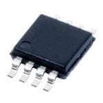
| 供应商器件封装 | 8-MSOP-PowerPad |
| 其它名称 | 296-30552-6 |
| 包装 | Digi-Reel® |
| 商标 | Texas Instruments |
| 安装类型 | 表面贴装 |
| 安装风格 | SMD/SMT |
| 封装 | Reel |
| 封装/外壳 | 8-TSSOP,8-MSOP(0.118",3.00mm 宽)裸焊盘 |
| 封装/箱体 | HVSSOP-8 |
| 工作温度 | -40°C ~ 85°C |
| 工作温度范围 | - 40 C to + 85 C |
| 工厂包装数量 | 2500 |
| 应用 | USB 专用充电端口(DCP),电源开关 |
| 开关数量 | Single |
| 最小工作温度 | - 40 C |
| 标准包装 | 1 |
| 电压-电源 | 4.5 V ~ 5.5 V |
| 电流-电源 | 180µA |
| 电源电压-最大 | 5.5 V |
| 电源电压-最小 | 4.5 V |
| 电源电流 | 230 uA |
| 系列 | TPS2511 |


- 商务部:美国ITC正式对集成电路等产品启动337调查
- 曝三星4nm工艺存在良率问题 高通将骁龙8 Gen1或转产台积电
- 太阳诱电将投资9.5亿元在常州建新厂生产MLCC 预计2023年完工
- 英特尔发布欧洲新工厂建设计划 深化IDM 2.0 战略
- 台积电先进制程称霸业界 有大客户加持明年业绩稳了
- 达到5530亿美元!SIA预计今年全球半导体销售额将创下新高
- 英特尔拟将自动驾驶子公司Mobileye上市 估值或超500亿美元
- 三星加码芯片和SET,合并消费电子和移动部门,撤换高东真等 CEO
- 三星电子宣布重大人事变动 还合并消费电子和移动部门
- 海关总署:前11个月进口集成电路产品价值2.52万亿元 增长14.8%


PDF Datasheet 数据手册内容提取
Product Sample & Technical Tools & Support & Folder Buy Documents Software Community TPS2511 SLUSB18A–JUNE2012–REVISEDAUGUST2016 TPS2511 USB Dedicated Charging Port Controller and Current Limiting Power Switch 1 Features 3 Description • SupportsaUSBDCPShortingD+LinetoD–Line The TPS2511 device is a USB-dedicated charging 1 port (DCP) controller and current-limiting power • SupportsaUSBDCPApplying2VonD+Line switch. An auto-detect feature monitors USB data line and2.7VonD– Line(oraUSBDCPApplying voltage, and automatically provides the correct 2.7VonD+Lineand2VonD–Line) electrical signatures on the data lines to charge • SupportsaUSBDCPApplying1.2VonD+and compliant devices among the following dedicated D–Lines chargingschemes: • AutomaticallySwitchD+andD– Lines 1. Divider DCP, required to apply 2.7 V and 2 V on ConnectionsforanAttachedDevice theD+andD– linesrespectivelyor2Vand2.7V ontheD+andD– linesrespectively • HiccupModeforOutputShort-CircuitProtection 2. BC1.2 DCP, required to short the D+ line to the • Provides CSPinforUSBCableCompensation D–line • ProgrammableCurrentLimit(ILIM_SETPin) 3. 1.2VonbothD+andD–lines • Accurate±10%CurrentLimitat2.3A(Typical) The TPS2511 is a 70-mΩ power-distribution switch • 70-mΩ (Typical)High-SideMOSFET intended for applications where heavy capacitive • CompatibleWithUSB2.0and3.0PowerSwitch loads and short circuits are likely to be encountered. Requirements This device also provides hiccup mode when the output (OUT) voltage is less than 3.8 V (typical) or • OperatingRange:4.5Vto5.5V when an overtemperature protection occurs during an • Availablein8-PinMSOP-PowerPAD™Package overload condition. Accurate and programmable current limit provides flexibility and convenience for 2 Applications applications. The TPS2511 provides a CS pin for • VehicleUSBPowerChargers USBcableresistancecompensationandanENpinto controlthedeviceturnonandturnoff. • AC-DCWallAdapterWithUSBPorts • OtherUSBChargers DeviceInformation(1) PARTNUMBER PACKAGE BODYSIZE(NOM) TPS2511 MSOP-PowerPAD(8) 3.00mm×3.00mm (1) For all available packages, see the orderable addendum at theendofthedatasheet. SimplifiedSchematic 5.0VOUT 5.0V TPS2511 VBUS 1 GND OUT 8 AC-to-DCo Cronverter COUT 2 ILIM_SET DM 7 D− ector Buck DC-to-DC nn Converter 3 IN DP 6 D+ Co B S FB 4 CS EN 5 GND U PAD CUSB RILIM GND Power Supply Copyright © 2016,Texas Instruments Incorporated 1 An IMPORTANT NOTICE at the end of this data sheet addresses availability, warranty, changes, use in safety-critical applications, intellectualpropertymattersandotherimportantdisclaimers.PRODUCTIONDATA.
TPS2511 SLUSB18A–JUNE2012–REVISEDAUGUST2016 www.ti.com Table of Contents 1 Features.................................................................. 1 7.4 DeviceFunctionalModes........................................15 2 Applications........................................................... 1 8 ApplicationandImplementation........................ 19 3 Description............................................................. 1 8.1 ApplicationInformation............................................19 4 RevisionHistory..................................................... 2 8.2 TypicalApplication..................................................19 5 PinConfigurationandFunctions......................... 3 9 PowerSupplyRecommendations...................... 22 6 Specifications......................................................... 4 10 Layout................................................................... 23 6.1 AbsoluteMaximumRatings......................................4 10.1 LayoutGuidelines.................................................23 6.2 ESDRatings..............................................................4 10.2 LayoutExample....................................................23 6.3 RecommendedOperatingConditions.......................4 11 DeviceandDocumentationSupport................. 24 6.4 ThermalInformation..................................................5 11.1 DocumentationSupport........................................24 6.5 ElectricalCharacteristics...........................................5 11.2 ReceivingNotificationofDocumentationUpdates24 6.6 SwitchingCharacteristics..........................................6 11.3 CommunityResources..........................................24 6.7 TypicalCharacteristics..............................................8 11.4 Trademarks...........................................................24 7 DetailedDescription.............................................. 9 11.5 ElectrostaticDischargeCaution............................24 7.1 Overview...................................................................9 11.6 Glossary................................................................24 7.2 FunctionalBlockDiagram.......................................10 12 Mechanical,Packaging,andOrderable Information........................................................... 24 7.3 FeatureDescription.................................................11 4 Revision History ChangesfromOriginal(June2012)toRevisionA Page • AddedESDRatingstable,FeatureDescriptionsection,DeviceFunctionalModes,ApplicationandImplementation section,PowerSupplyRecommendationssection,Layoutsection,DeviceandDocumentationSupportsection,and Mechanical,Packaging,andOrderableInformationsection ................................................................................................. 1 • DeletedOrderingInformationtable,seePOAattheendofthedocument............................................................................ 1 2 SubmitDocumentationFeedback Copyright©2012–2016,TexasInstrumentsIncorporated ProductFolderLinks:TPS2511
TPS2511 www.ti.com SLUSB18A–JUNE2012–REVISEDAUGUST2016 5 Pin Configuration and Functions DGNPackage 8-PinMSOPWithPowerPAD™ TopView GND 1 8 OUT ILIM_SET 2 7 DM IN 3 6 DP CS 4 5 EN PinFunctions PIN TYPE(1) DESCRIPTION NAME NO. Active-low,open-drainoutput.WhenOUTcurrentismorethanapproximatelyhalfofthe CS 4 O currentlimitsetbyaresistoronILIM_SETpin,theoutputisactivelow.Maximumsink currentis10mA. ConnectedtotheD–orD+lineofUSBconnector.Providethecorrectvoltagewithan DM 7 I/O attachedportableequipmentforDCPdetection,highimpedancewhiledisabled. ConnectedtotheD+orD–lineofUSBconnector.Providethecorrectvoltagewithan DP 6 I/O attachedportableequipmentforDCPdetection,highimpedancewhiledisabled. Logic-levelcontrolinput.Whenitishigh,turnspowerswitchon,whenitislow,turnspower EN 5 I switchoffandturnsDPandDMintothehighimpedancestate. GND 1 G Groundconnection. ExternalresistorusedtosetcurrentlimitingThreshold.TIrecommends16.9kΩ≤R ≤ ILIM_SET 2 I ILIM_SET 750kΩ. Powersupplyinputvoltageconnectedtothepowerswitch.Connectaceramiccapacitorwith IN 3 P avalueof0.1-µForgreaterfromtheINpintoGNDasclosetothedeviceaspossible. OUT 8 O Power-switchoutput.ConnecttoVBUSofUSB PowerPAD PowerPAD G Groundconnection. (1) G=Ground,I=Input,O=Output,P=Power Copyright©2012–2016,TexasInstrumentsIncorporated SubmitDocumentationFeedback 3 ProductFolderLinks:TPS2511
TPS2511 SLUSB18A–JUNE2012–REVISEDAUGUST2016 www.ti.com 6 Specifications 6.1 Absolute Maximum Ratings overoperatingfree-airtemperaturerange(unlessotherwisenoted)(1) MIN MAX UNIT IN Supplyvoltage –0.3 7 EN,ILIM_SET Inputvoltage –0.3 7 OUT,CS –0.3 7 Voltage INtoOUT –7 7 V –0.3 IN+0.3or DPoutputvoltage DMoutput 5.7 –0.3 IN+0.3or DPinputvoltage DMinput 5.7 DPinputcurrent, Continuousoutputsinkcurrent 35 DMinputcurrent DPoutput Continuousoutputsourcecurrent 35 Current current,DM mA outputcurrent CS Continuousoutputsinkcurrent 10 ILIM_SET Continuousoutputsourcecurrent Internallylimited Operatingjunctiontemperature,T Internallylimited J Temperature Storagetemperature,T –65 150 °C stg (1) StressesbeyondthoselistedunderAbsoluteMaximumRatingsmaycausepermanentdamagetothedevice.Thesearestressratings only,whichdonotimplyfunctionaloperationofthedeviceattheseoranyotherconditionsbeyondthoseindicatedunderRecommended OperatingConditions.Exposuretoabsolute-maximum-ratedconditionsforextendedperiodsmayaffectdevicereliability. 6.2 ESD Ratings VALUE UNIT Human-bodymodel(HBM),per Allpinsexcept6and7 ±2000 V Electrostaticdischarge ANSI/ESDA/JEDECJS-001(1) Pins6and7 ±7500 V (ESD) Charged-devicemodel(CDM),perJEDECspecificationJESD22-C101(2) ±500 (1) JEDECdocumentJEP155statesthat500-VHBMallowssafemanufacturingwithastandardESDcontrolprocess. (2) JEDECdocumentJEP157statesthat250-VCDMallowssafemanufacturingwithastandardESDcontrolprocess. 6.3 Recommended Operating Conditions voltagesarereferencedtoGND(unlessotherwisenoted),positivecurrentareintopins. MIN MAX UNIT V InputvoltageofIN 4.5 5.5 IN V InputvoltageofCS 0 5.5 CS V InputvoltageofEN 0 5.5 V EN V DPdatalineinputvoltage 0 5.5 DP V DMdatalineinputvoltage 0 5.5 DM I Continuoussink/sourcecurrent ±10 DP I Continuoussink/sourcecurrent ±10 mA DM I Continuoussinkcurrent 2 CS I ContinuousoutputcurrentofOUT 2.2 A OUT R Aresistorofcurrentlimit,ILIM_SETtoGND 16.9 750 kΩ ILIM_SET T Operatingjunctiontemperature –40 125 ºC J 4 SubmitDocumentationFeedback Copyright©2012–2016,TexasInstrumentsIncorporated ProductFolderLinks:TPS2511
TPS2511 www.ti.com SLUSB18A–JUNE2012–REVISEDAUGUST2016 6.4 Thermal Information TPS2511 THERMALMETRIC(1) DGN UNIT (MSOP-PowerPAD) 8PINS R Junction-to-ambientthermalresistance 65.2 °C/W θJA R Junction-to-case(top)thermalresistance 53.3 °C/W θJC(top) R Junction-to-boardthermalresistance 36.9 °C/W θJB ψ Junction-to-topcharacterizationparameter 3.9 °C/W JT ψ Junction-to-boardcharacterizationparameter 36.6 °C/W JB R Junction-to-case(bottom)thermalresistance 13.4 °C/W θJC(bot) (1) Formoreinformationabouttraditionalandnewthermalmetrics,seetheSemiconductorandICPackageThermalMetricsapplication report. 6.5 Electrical Characteristics Conditionsare–40°C≤(T =T )≤125°C,4.5V≤V ≤5.5V,V =V andR =22.1kΩ.Positivecurrentareinto J A IN EN IN ILIM_SET pins.Typicalvaluesareat25°C.AllvoltagesarewithrespecttoGND(unlessotherwisenoted). PARAMETER TESTCONDITIONS MIN TYP MAX UNIT POWERSWITCH I =2A 70 120 OUT Staticdrain-sourceON-state R I =2A,–40ºC≤(T =T )≤85ºC 70 105 mΩ DS(on) resistance OUT J A I =2A,T =T =25ºC 70 84 OUT J A I Reverseleakagecurrent V =5.5V,V =V =0V 0.01 2 µA REV OUT IN EN DISCHARGE R Dischargeresistance V =4V 400 500 630 Ω DCHG OUT CURRENTLIMIT R =44.2kΩ 1060 1160 1270 ILIM_SET I OUTshort-circuitcurrentlimit R =22.1kΩ 2110 2300 2550 mA OS ILIM_SET R =16.9kΩ 2760 3025 3330 ILIM_SET HICCUPMODE OUTvoltagethresholdofgoing V V =5V,R =210kΩ 3.6 3.8 4.1 V OUT_SHORT intohiccupmode IN ILIIM_SET UNDERVOLTAGELOCKOUT V INUVLOthresholdvoltage,rising 3.9 4.1 4.3 V UVLO Hysteresis(1) 100 mV SUPPLYCURRENT V =0V,V =5.5V, I Disabled,INsupplycurrent EN IN 0.1 2 IN_OFF –40ºC≤TJ≤85ºC µA I Enabled,INsupplycurrent V =V ,R =210kΩ 180 230 IN_ON EN IN ILIM_SET THERMALSHUTDOWN Notincurrentlimit 155 Temperaturerisingthreshold(1) Incurrentlimit 135 ºC Hysteresis (1) 10 OUTCURRENTDETECTION Loaddetectioncurrentthreshold, RILIM_SET=22.1kΩ 1060 IHCC_TH rising (1) R =44.2kΩ 560 mA ILIM_SET Loaddetectioncurrent RILIM_SET=22.1kΩ 230 IHCC_TH_HYS Hysteresis(1) R =44.2kΩ 120 mA ILIM_SET V CSoutputactive-lowvoltage(1) I =1mA 0 80 140 mV CS CS (1) Specifiedbydesign.Notproductiontested. Copyright©2012–2016,TexasInstrumentsIncorporated SubmitDocumentationFeedback 5 ProductFolderLinks:TPS2511
TPS2511 SLUSB18A–JUNE2012–REVISEDAUGUST2016 www.ti.com Electrical Characteristics (continued) Conditionsare–40°C≤(T =T )≤125°C,4.5V≤V ≤5.5V,V =V andR =22.1kΩ.Positivecurrentareinto J A IN EN IN ILIM_SET pins.Typicalvaluesareat25°C.AllvoltagesarewithrespecttoGND(unlessotherwisenoted). PARAMETER TESTCONDITIONS MIN TYP MAX UNIT ENABLEINPUT(EN) V ENthresholdvoltage,falling 0.9 1.1 1.65 V EN_TRIP V Hysteresis 100 200 300 mV EN_TRIP_HYS I Leakagecurrent V =0VorV =5.5V –0.5 0.5 µA EN EN EN BC1.2DCPMODE(SHORTMODE) R DPandDMshortingresistance V =0.8V,I =1mA 125 200 Ω DPM_SHORT DP DM ResistancebetweenDP/DMand R V =0.8V 400 700 1300 kΩ DCHG_SHORT GND DP VoltagethresholdonDPunder V whichthedevicegoesbackto 310 330 350 mV DPL_TH_DETACH dividermode V Hysteresis 50 (1) mV DPL_TH_DETACH_HYS DIVIDERMODE V DPoutputvoltage V =5V 2.57 2.7 2.84 DP_2.7V IN V V DMoutputvoltage V =5V 1.9 2 2.1 DM_2.0V IN R DPoutputimpedance I =–5µA 24 30 40 DP_PAD1 DP kΩ R DMoutputimpedance I =–5µA 24 30 40 DM_PAD1 DM 1.2V/1.2VMODE V DPoutputvoltage V =5V 1.12 1.2 1.28 V DP_1.2V IN V DMoutputvoltage V =5V 1.12 1.2 1.28 V DM_1.2V IN R DPoutputimpedance I =–5uA 80 105 130 kΩ DP_PAD2 DP R DMoutputimpedance I =–5uA 80 105 130 kΩ DM_PAD2 DM 6.6 Switching Characteristics Conditionsare–40°C≤(T =T )≤125°C,4.5V≤V ≤5.5V,V =V andR =22.1kΩ.Positivecurrentareinto J A IN EN IN ILIM_SET pins.Typicalvaluesareat25°C.AllvoltagesarewithrespecttoGND(unlessotherwisenoted). PARAMETER TESTCONDITIONS MIN TYP MAX UNIT POWERSWITCH C =1µF,R =100Ω,V =5V t OUTvoltagerisetime L L IN 1 1.5 r seeFigure1,Figure3 ms C =1µF,R =100Ω,V =5V t OUTvoltagefalltime L L IN 0.2 0.35 0.5 f seeFigure1,Figure3 CURRENTLIMIT t Shortcircuitresponsetime(1) VIN=5V,RL=50mΩ,2inches 1.5 µs IOS leadlength,SeeFigure4 HICCUPMODE t ON-timeofhiccupmode(1) V =5V,R =0 16 ms OS_DEG IN L t OFF-timeofhiccupmode(1) V =5V,R =0 12 s SC_TURN_OFF IN L OUTCURRENTDETECTION t CSdeglitchtimeduringturningon(1) I =1mA 8 ms CS_EN CS ENABLEINPUT(EN) ton OUTvoltageturnontime CL=1µF,RL=100Ω, 2.6 5 ms t OUTvoltageturnofftime seeFigure1,Figure2 1.7 3 off (1) Specifiedbydesign.Notproductiontested. 6 SubmitDocumentationFeedback Copyright©2012–2016,TexasInstrumentsIncorporated ProductFolderLinks:TPS2511
TPS2511 www.ti.com SLUSB18A–JUNE2012–REVISEDAUGUST2016 OUT R C L L Figure1. OutputRiseandFallTestLoad V 50% 50% EN t on t off 90% V OUT 10% Figure2. EnableTiming,ActiveHighEnable 90% V OUT t t r f 10% Figure3. PowerOnandPowerOff I OS I OUT t IOS Figure4. OutputShort-CircuitParameters Copyright©2012–2016,TexasInstrumentsIncorporated SubmitDocumentationFeedback 7 ProductFolderLinks:TPS2511
TPS2511 SLUSB18A–JUNE2012–REVISEDAUGUST2016 www.ti.com 6.7 Typical Characteristics 3.2 2.4 VDM VDP VIN=5V VIN=5V, RILIM_SET=16.9kW ge - V 2.8 d -Am 1.6 a e ut Volt Disabl M Outp 2.4 urrent, 0.8 D C Pand 2 upply 0 D S 1.6 -2 -40 -20 0 20 40 60 80 100 120 -40 -20 0 20 40 60 80 100 120 TJ- Junction Temperature - °C TJ- Junction Temperature - °C Figure5. DPandDMOutputVoltagevsTemperature Figure6. SupplyCurrentDisabledvsTemperature 230 3 VIN=5V VIN=5V RILIM_SET=20kW RILIM_SET=22.1kW 2.8 A 210 m d - A able mit - 2.6 nt, En 190 ent Li urre Curr 2.4 upply C 170 I- CC S 2.2 RILIM=16.9kW RILIM=210kW 150 2 -40 -20 0 20 40 60 80 100 120 -40 -20 0 20 40 60 80 100 120 TJ- Junction Temperature - °C TJ- Junction Temperature - °C Figure7. SupplyCurrentEnabledvsTemperature Figure8.CurrentLimitvsTemperature 120 VIN=5V,IOUT=2A 100 W m - N) 80 O S( D R 60 40 -40 -20 0 20 40 60 80 100 120 TJ- Junction Temperature - °C Figure9.PowerSwitchON-Resistance(R )vsTemperature DS(ON) 8 SubmitDocumentationFeedback Copyright©2012–2016,TexasInstrumentsIncorporated ProductFolderLinks:TPS2511
TPS2511 www.ti.com SLUSB18A–JUNE2012–REVISEDAUGUST2016 7 Detailed Description 7.1 Overview The following overview references various industry standards. TI always recommends consulting the latest standardtoensurethemostrecentandaccurateinformation. Rechargeable portable equipment requires an external power source to charge its batteries. USB ports are convenient locations for charging because of an available 5-V power source. Universally accepted standards are required to ensure host and client-side devices meet the power management requirements. Traditionally, USB host ports following the USB 2.0 Specification must provide at least 500 mA to downstream client-side devices. Because multiple USB devices can be attached to a single USB port through a bus-powered hub, it is the responsibility of the client-side device to negotiate the power allotment from the host to ensure the total current drawdoesnotexceed500mA.TheTPS2511provides100mAofcurrenttoeachUSBdevice.EachUSBdevice can subsequently request more current, which is granted in steps of 100 mA up 500 mA total. The host may grantordenytherequestbasedontheavailablecurrent. Additionally, the success of the USB technology makes the micro-USB connector a popular choice for wall adapter cables. This allows a portable device to charge from both a wall adapter and USB port with only one connector. One common difficulty has resulted from this. As USB charging has gained popularity, the 500-mA minimum defined by the USB 2.0 Specification or 900 mA defined in the USB 3.0 Specification, has become insufficient for many handsets, tablets, and personal media players (PMP), which have a higher-rated charging current. Wall adapters and car chargers can provide much more current than 500 mA or 900 mA to fast charge portable devices. Several new standards have been introduced defining protocol handshaking methods that allow host and client devices to acknowledge and draw additional current beyond the 500 mA (defined in the USB 2.0 Specification) or 900 mA (defined in the USB 3.0 Specification) minimum while using a single micro-USB input connector. TheTPS2511supportsthreeofthemostcommonprotocols: • USBBatteryChargingSpecification,Revision1.2(BC1.2) • ChineseTelecommunicationsIndustryStandardYD/T1591-2009 • DividerMode In these protocols there are three types of charging ports defined to provide different charging current to client- sidedevices.Thesechargingportsaredefinedas: • Standarddownstreamport(SDP) • Chargingdownstreamport(CDP) • Dedicatedchargingport(DCP) The BC1.2 Specification defines a charging port as a downstream facing USB port that provides power for chargingportableequipment. Table1listsdifferentportoperatingmodesaccordingtotheBC1.2Specification. Table1.OperatingModesTable MAXIMUMALLOWABLECURRENT SUPPORTSUSB2.0 PORTTYPE DRAWN COMMUNICATION BYPORTABLEEQUIPMENT(A) SDP(USB2.0) Yes 0.5 SDP(USB3.0) Yes 0.9 CDP Yes 1.5 DCP No 1.5 The BC1.2 Specification defines the protocol necessary to allow portable equipment to determine what type of port it is connected to so that it can allot its maximum allowable current drawn. The hand-shaking process is two steps. During step one, the primary detection, the portable equipment outputs a nominal 0.6-V output on its D+ line and reads the voltage input on its D– line. The portable device concludes it is connected to a SDP if the voltage is less than the nominal data detect voltage of 0.3 V. The portable device concludes that it is connected to a Charging Port if the D– voltage is greater than the nominal data detect voltage of 0.3 V and less than 0.8 V. Copyright©2012–2016,TexasInstrumentsIncorporated SubmitDocumentationFeedback 9 ProductFolderLinks:TPS2511
TPS2511 SLUSB18A–JUNE2012–REVISEDAUGUST2016 www.ti.com Thesecondstep,thesecondarydetection,isnecessaryforportableequipmenttodeterminebetweenaCDPand a DCP. The portable device outputs a nominal 0.6-V output on its D– line and reads the voltage input on its D+ line. The portable device concludes it is connected to a CDP if the data line being remains is less than the nominal data detect voltage of 0.3 V. The portable device concludes it is connected to a DCP if the data line beingreadisgreaterthanthenominaldatadetectvoltageof0.3Vandlessthan0.8V. 7.2 Functional Block Diagram CurrentSense IN CS OUT Current ILIM_SET Disable+UVLO Limit GND 8-ms Charge Deglitch Pump EN Driver UVLO Thermal Hiccup Sense CS REF + S1 DP S2 Auto Detect S4 S3 DM 2.0V 2.7V + + + + 1.2V – – – – Copyright © 2016,Texas Instruments Incorporated 10 SubmitDocumentationFeedback Copyright©2012–2016,TexasInstrumentsIncorporated ProductFolderLinks:TPS2511
TPS2511 www.ti.com SLUSB18A–JUNE2012–REVISEDAUGUST2016 7.3 Feature Description 7.3.1 OvercurrentProtection During an overload condition, the TPS2511 maintains a constant output current and reduces the output voltage accordingly. If the output voltage falls to less than 3.8 V for 16 ms, the TPS2511 turns off the output for a period of 12 seconds as shown in Figure 10. This operation is referred to as hiccup mode. The device stays in hiccup mode (power cycling) until the overload condition is removed. Therefore the average output current is significantlyreducedtogreatlyimprovethethermalstressofthedevicewhiletheOUTpinisshorted. ON OFF t SC_TURN_OFF I OC t OS_DEG I OUT(av) 0A UDG-12108 Figure10. OUTPinShort-CircuitCurrentinHiccupMode Two possible overload conditions can occur. In the first condition, the output has been shorted before the device is enabled or before the voltage of IN has been applied. The TPS2511 senses the short and immediately switches into hiccup mode of constant-current limiting. In the second condition, a short or an overload occurs while the device is enabled. At the instant the overload occurs, high currents may flow for several microseconds beforethecurrentlimitcircuitcanreact.Thedeviceoperatesinconstant-currentmodeforaperiodof16msafter thecurrentlimitcircuithasresponded,thenswitchesintohiccupmode(powercycling). Copyright©2012–2016,TexasInstrumentsIncorporated SubmitDocumentationFeedback 11 ProductFolderLinks:TPS2511
TPS2511 SLUSB18A–JUNE2012–REVISEDAUGUST2016 www.ti.com Feature Description (continued) 7.3.2 CurrentLimitThreshold The TPS2511 has a current limiting threshold that is externally programmed with a resistor. Equation 1 and Figure11helpdeterminethetypicalcurrentlimitthreshold. 51228 I = OS_TYP R ILIM where • I isinmAandR isinkΩ OS_TYP ILIM • I hasabetteraccuracyifR islessthan210kΩ (1) OS_TYP ILIM 3.5 VIN= 5 V IOS_TYP 3 A mit - 2.5 Li nt e r 2 r u C uit c 1.5 r Ci rt o h 1 S T U O 0.5 0 10 60 110 160 210 260 310 360 410 460 510 560 610 660700 Current-Limit Programming Resistor of ILIM_SET - kW Figure11. TypicalCurrentLimitvsProgrammingResistor 7.3.3 Current-SensingReport(CS) The CS open-drain output is asserted immediately when the OUT pin current is more than about half of the current limit set by a resistor on ILIM_SET pin. Built-in hysteresis improves the ability to resist current noise on the OUT pin. The CS output is active low. The recommended operating sink current is less than 2 mA and maximumsinkcurrentis10mA. 7.3.4 UndervoltageLockout(UVLO)andEnable(EN) The undervoltage lockout (UVLO) circuit disables the power switch and other functional circuits until the input voltage reaches the UVLO turnon threshold. Built-in hysteresis prevents unwanted oscillations on the output due toinputvoltagedropfromlargecurrentsurges. The logic input of the EN pin disables all of the internal circuitry while maintaining the power switch off. A logic- high input on the EN pin enables the driver, control circuits, and power switch. The EN input voltage is compatiblewithbothTTLandCMOSlogiclevels. 7.3.5 SoftStart,ReverseBlocking,andDischargeOutput The power MOSFET driver incorporates circuitry that controls the rise and fall times of the output voltage to limit large current and voltage surges on the input supply, and provides built-in soft-start functionality. The TPS2511 power switch blocks current from the OUT pin to the IN pin when turned off by the UVLO or disabled. The TPS2511 includes an output discharge function. A 500-Ω (typical) discharge resistor dissipates stored charge and leakage current on the OUT pin when the device is in UVLO or disabled. However as this circuit is biased fromtheINpin,theoutputdischargeisnotactivewhentheinputapproaches0V. 12 SubmitDocumentationFeedback Copyright©2012–2016,TexasInstrumentsIncorporated ProductFolderLinks:TPS2511
TPS2511 www.ti.com SLUSB18A–JUNE2012–REVISEDAUGUST2016 Feature Description (continued) 7.3.6 ThermalSense The TPS2511 provides thermal protection from two independent thermal-sensing circuits that monitor the operating temperature of the power distribution switch and turnoff for 12 s (typical) if the temperature exceeds recommended operating conditions. The device operates in constant-current mode during an overcurrent condition and OUT pin voltage is greater than 3.8 V (typical), which has a relatively large voltage drop across power switch. The power dissipation in the package is proportional to the voltage drop across the power switch, so the junction temperature rises during the overcurrent condition. The first thermal sensor turns off the power switch when the die temperature exceeds 135°C and the device is within the current limit. The second thermal sensor turns off the power switch when the die temperature exceeds 155°C regardless of whether the power switch is in current limit. Hysteresis is built into both thermal sensors, and the switch turns on after the device hascooledapproximately10°C.Theswitchcontinuestocycleoffandonuntilthefaultisremoved. 7.3.7 V VoltageDropCompensation BUS Figure12showsaUSBchargingdesignusingtheTPS2511.Ingeneral,V hassomevoltagelossduetoUSB BUS cable resistance and TPS2511 power switch ON-state resistance. The sum of voltage loss is likely several hundred millivolts from 5-V to V that is the input voltage of PD while the high charging current charges OUT PD_IN the PD. For example, in Figure 13, assuming that the loss resistance is 170 mΩ (includes 100 mΩ of USB cable resistance and 70 mΩ of power switch resistance) and 5 V is 5 V, the input voltage of PD (V ) is about OUT PD_IN 4.66Vat2A(seeFigure13). 5VOUT 5.0V VPD_IN 100kW R1 TPS2511 IOUT VBUS 1 GND OUT 8 AC-to-DCo rConverter 2 ILIM_SET DM 7 D− ector IOUT BucCko DnvCe-rttoe-rDC COUT R2 R4 3 IN DP 6 D+ Conn Portable Device B S GND U 4 CS EN 5 Cable FB PAD CUSB 0.1mF R3 RILIM GND Power Supply Copyright © 2016,Texas Instruments Incorporated Figure12. TPS2511ChargingSystemSchematicDiagram The charging current of most portable devices is less than their maximum charging current while V is less PD_IN than the certain voltage value. Furthermore, actual charging current of PD decreases with input voltage falling. Therefore, a portable devices cannot accomplish a fast charge with its maximum charging rated current if V BUS voltage drop across the power path is not compensated at the high charging current. The TPS2511 provides CS pin to report the high charging current for USB chargers to increase the 5-V voltage. This is shown by the OUT solidlinesofFigure13. Copyright©2012–2016,TexasInstrumentsIncorporated SubmitDocumentationFeedback 13 ProductFolderLinks:TPS2511
TPS2511 SLUSB18A–JUNE2012–REVISEDAUGUST2016 www.ti.com Feature Description (continued) 5.25 5.15 5.00 V) ( 4.75 e g a olt 4.66 V ut p ut O 5VOUTwithcompensation VPD_INwithcompensation 5VOUTwithoutcompensation VPD_INwithoutcompensation 0 0.5 1.0 1.5 2.0 2.5 OutputCurrent(A) UDG-12109 Figure13. TPS2511CSFunction Equation2throughEquation5refertoFigure12. ThepowersupplyoutputvoltageiscalculatedinEquation2. (R1+R2+R3)´VFB 5VOUT = R 3 (2) 5 V and V are known. If R is given and R is fixed, R can be calculated. The 5 V voltage change with OUT FB 3 1 2 OUT compensationisshowninEquation3andEquation4. (R2+R3)´R1´VFB DV = R3´R4 (3) æ5V R öR ´V ΔV= ç OUT - 1÷ 1 FB V R R è FB 3ø 4 (4) IfR islessthanR ,thenEquation4canbesimplifiedasEquation5. 1 3 5V ´R DV » OUT 1 R 4 (5) 7.3.8 DivideModeSelectionof5-Wand10-WUSBChargers The TPS2511 provides two types of connections between the DP pin and the DM pin and between the D+ data line and the D– data line of the USB connector for a 5-W USB charger and a 10-W USB charger with a single USB port. For a 5-W USB charger, the DP pin is connectd to the D– line and the DM pin is connected to the D+ line. This is shown in Figure 16 and Figure 17. It is necessary to apply DP and DM to D+ and D– of USB connector for 10-W USB chargers. See Figure 14 and Figure 15. Table 2 shows different charging schemes for both5-Wand10-WUSBchargersolutions Table2.ChargingSchemesfor5-Wand10-WUSBChargers USBCHARGERTYPE CONTAININGCHARGINGSCHEMES 5-W Divider1 1.2VonbothD+andD–Lines BC1.2DCP 10-W Divider2 1.2VonbothD+andD–Lines BC1.2DCP 14 SubmitDocumentationFeedback Copyright©2012–2016,TexasInstrumentsIncorporated ProductFolderLinks:TPS2511
TPS2511 www.ti.com SLUSB18A–JUNE2012–REVISEDAUGUST2016 TPS2511 5.0V Power 3 IN OUT 8 VBUS 5.0V TPS2511 Supply 5 EN DM 7 D- nnector SPuopwpelyr 3 IN OUT 8 VDB-US ctor 4 CS DP 6 D+ Co 5 EN DM 7 nne B D+ o S 4 CS DP 6 C GND U B 2 ILIM_SET GND 1 S GND U 2 ILIM_SET GND 1 PAD RILIM PAD R ILIM UDG-12104 UDG-12105 Figure14. 10-WUSBChargerApplicationWith Figure15. 10-WUSBChargerApplicationWithout PowerSwitch PowerSwitch TPS2511 5.0V Power 3 IN OUT 8 VBUS 5.0V TPS2511 Supply 5 EN DM 7 D- nnector SPuopwpelyr 3 IN OUT 8 VDB-US ctor D+ Co 5 EN DM 7 ne 4 CS DP 6 n B D+ o GND US 4 CS DP 6 BC 2 ILIM_SET GND 1 S GND U 2 ILIM_SET GND 1 PAD RILIM PAD R ILIM UDG-12106 UDG-12107 Figure16. 5-WUSBChargerApplicationWith Figure17. 5-WUSBChargerApplicationWithout PowerSwitch PowerSwitch 7.4 Device Functional Modes 7.4.1 DedicatedChargingPort(DCP) A dedicated charging port (DCP) is a downstream port on a device that outputs power through a USB connector, butisnotcapableofenumeratingadownstreamdevice,whichgenerallyallowsportabledevicestofastchargeat their maximum rated current. A USB charger is a device with a DCP, such as a wall adapter or car power adapter. A DCP is identified by the electrical characteristics of its data lines. The following DCP identification circuitsareusuallyusedtomeetthehandshakingdetectionsofdifferentportabledevices. 7.4.1.1 ShorttheD+LinetotheD– Line The USB BC1.2 Specification and the Chinese Telecommunications Industry Standard YD/T 1591-2009 define that the D+ and D– data lines must be shorted together with a maximum series impedance of 200 Ω. This is showninFigure18. Copyright©2012–2016,TexasInstrumentsIncorporated SubmitDocumentationFeedback 15 ProductFolderLinks:TPS2511
TPS2511 SLUSB18A–JUNE2012–REVISEDAUGUST2016 www.ti.com Device Functional Modes (continued) V BUS V BUS 5.0V or D− ct e n 200 W(max) D+ on C B S GND U GND UDG-12100 Figure18. DCPShortMode 7.4.1.2 Divider1(DCPApplying2VonD+Lineand2.7VonD– Line)orDivider2(DCPApplying2.7Von D+Lineand2VonD– Line) There are two charging schemes for divider DCP. They are named after Divider1 and Divider2 DCPs that are shown in Figure 19and Figure 20. The Divider1 charging scheme is used for 5-W adapters, Divider1 applies 2 V to the D+ line and 2.7 V to the D– data line. The Divider2 charging scheme is used for 10-W adapters and applies2.7VontheD+lineand2VisappliedontheD–line. V V BUS V BUS V BUS BUS 5.0V 5.0V D− or D− or ct ct e e n n n n D+ o D+ o C C B B 2.7V 2.0V S 2.0V 2.7V S GND U GND U + + + + – – – – GND UDG-12101 GND UDG-12102 Figure19. Divider1DCP Figure20. Divider2DCP 7.4.1.3 Applying1.2VtotheD+Lineand1.2VtotheD–Line As shown in Figure 21, some tablet USB chargers require 1.2 V on the shorted data lines of the USB connector. ThemaximumresistancebetweentheD+lineandtheD– lineis200Ω. 16 SubmitDocumentationFeedback Copyright©2012–2016,TexasInstrumentsIncorporated ProductFolderLinks:TPS2511
TPS2511 www.ti.com SLUSB18A–JUNE2012–REVISEDAUGUST2016 Device Functional Modes (continued) V V BUS BUS 5.0V or D− ct e n n 200W(max) D+ o C B S GND U + 1.2V – GND UDG-12103 Figure21. DCPApplying1.2VtotheD+Lineand1.2VtotheD–Line The TPS2511 is a combination of a current-limiting USB power switch and an USB DCP identification controller. Applications include vehicle power charger, wall adapters with USB DCP and other USB chargers. The TPS2511 DCP controller has the auto-detect feature that monitors the D+ and D– line voltages of the USB connector, providing the correct electrical characteristics on the DP and DM pins for the correct detections of compliant portable devices to fast charge. These portable devices include smart phones, 5-V tablets, and personal media players. The TPS2511 power-distribution switch is intended for applications where heavy capacitive loads and short circuits are likely to be encountered, incorporating a 70-mΩ, N-channel MOSFET in a single package. This device provides hiccup mode when in current limit and OUT voltage is less than 3.8 V (typical) or an over- temperature protection occurs under an overload condition. Hiccup mode operation can reduce the output short- circuit current down to several milliamperes. The TPS2511 provides a logic-level enable EN pin to control the device turnon and turnoff and an open-drain output CS for compensating V to account for cable I × R voltage BUS loss. 7.4.2 DCPAuto-Detect The TPS2511 integrates an auto-detect feature to support divider mode, short mode and 1.2 V / 1.2 V mode. If a divider device is attached, 2.7 V is applied to the DP pin and 2 V is applied to the DM pin. If a BC1.2-compliant device is attached, the TPS2511 automatically switches into short mode. If a device compliant with the 1.2 V / 1.2 V charging scheme is attached, 1.2 V is applied on both the DP pin and the DM pin. The functional diagram ofDCPauto-detectfeatureisshowninFigure22. Copyright©2012–2016,TexasInstrumentsIncorporated SubmitDocumentationFeedback 17 ProductFolderLinks:TPS2511
TPS2511 SLUSB18A–JUNE2012–REVISEDAUGUST2016 www.ti.com Device Functional Modes (continued) OUT 5V 8 Divider2 V BUS S1,S2:ON S1 DM r S3,S4:OFF D– cto 6 e n ShortMode n D+ o S4:ON C S1,S2,S3:OFF B S2 S4 GND US 1.2VonDPand DM S3,S4:ON S3 DP S1,S2:OFF 7 + 2V + 2.7V + 1.2V GND – – – 1 TPS2511 GND UDG-12099 Figure22. TPS2511DCPAuto-DetectFunctionalDiagram 18 SubmitDocumentationFeedback Copyright©2012–2016,TexasInstrumentsIncorporated ProductFolderLinks:TPS2511
TPS2511 www.ti.com SLUSB18A–JUNE2012–REVISEDAUGUST2016 8 Application and Implementation NOTE Information in the following applications sections is not part of the TI component specification, and TI does not warrant its accuracy or completeness. TI’s customers are responsible for determining suitability of components for their purposes. Customers should validateandtesttheirdesignimplementationtoconfirmsystemfunctionality. 8.1 Application Information The TPS2511 is a USB-dedicated charging-port controller and power switch with cable compensation. It is typicallyusedforwalladapterorpowerbankasaUSBchargingcontrollerandovercurrentprotector. 8.2 Typical Application VIN IOUT 0.1mF TPS2511 100kW 100kW VBUS 3 IN OUT 8 or D– ct EN 5 EN DM 7 e n D+ on RLOAD C CS 4 CS DP 6 B S GND U 2 ILIM_SET GND 1 PAD 22 uF 22.1 kW Figure23. TestCircuitforSystemOperation 8.2.1 DesignRequirements Forthisdesignexample,requestIOS;Minimummustexceed2100mA. Whenchoosingthepowerswitch,TIrecommendsfollowingthesegeneralsteps: 1. Determine the voltage of the power rail, 3.3 V or 5 V, and then choose the operation range of power switch cancovepowerrail. 2. Determine the normal operation current; for example, the maximum allowable current drawn by portable equipment for USB 2.0 port is 500 mA, so the normal operation current is 500 mA and the minimum current limitofpowerswitchmustexceed500mAtoavoidfalsetriggerduringnormaloperation. 3. Determine the maximum allowable current provided by up-stream power, and then decide the maximum current limit of power switch that must lower it to ensure power switch can protect the up-stream power when overloadisencounteredattheoutputofpowerswitch. NOTE Choosing power switch with tighter current limit tolerance can loosen the up-stream power supplydesign. 8.2.2 DetailedDesignProcedure The user-programmable R resistor on the ILIMIT_SET pin sets the current limit. The TPS2511 uses an ILIM internal regulation loop to provide a regulated voltage on the ILIM_SET pin. The current limiting threshold is proportional to the current sourced out of the ILIM_SET pin. The recommended 1% resistor range for R is ILIM from 16.9 kΩ to 750 kΩ to ensure stability of the internal regulation loop, although not exceeding 210 kΩ results in a better accuracy. Many applications require that the minimum current limit remain above a certain current Copyright©2012–2016,TexasInstrumentsIncorporated SubmitDocumentationFeedback 19 ProductFolderLinks:TPS2511
TPS2511 SLUSB18A–JUNE2012–REVISEDAUGUST2016 www.ti.com Typical Application (continued) level or that the maximum current limit remain below a certain current level, so it is important to consider the tolerance of the overcurrent threshold when selecting a value for R . Equation 6 and Equation 7 calculate the ILIM resulting overcurrent thresholds for a given external resistor value (R ). The traces routing the R resistor to ILIM ILIM the TPS2511 must be as short as possible to reduce parasitic effects on the current limit accuracy. The equations along with Figure 24 and Figure 25 can be used to estimate the minimum and maximum variation of the current limit threshold for a predefined resistor value. This variation disregards the inaccuracy of the resistor itself. 51228 I = OS_MIN R 1.030 ILIM where • I isinmA OS_MIN • R isinkΩ (6) ILIM xxxxxx 51228 I = OS_MAX R 0.967 ILIM where • I isinmA OS_MAX • R isinkΩ (7) ILIM 3.6 600m V = 5 V V = 5 V I I I IN IN OS_TYP OS_MIN OS_MAX A 3 A 500m mit - mit - cuit Current Li 21..48 uit Current Li 430000mm r c ort Ci 1.2 rt Cir 200m h o S h UT T S O 0.6 OU 100m I I I OS_TYP OS_MIN OS_MAX 0 0 10 20 30 40 50 60 70 80 90 100 100 200 300 400 500 600 700 CurrentLimitProgrammingResistorofILIM_SET-kW CurrentLimitProgrammingResistorofILIM_SET-kW Figure24. CurrentLimitThresholdvsCurrentLimit Figure25. CurrentLimitThresholdvsCurrentLimit Resistance Resistance Forthisexampledesign,asshowninEquation8,I =2100mA. OS_MIN 51228 I = =2100mA OS_MIN R 1.03 ILIM (8) 1 1 æ 51228 ö1.03 æ51228ö1.03 RILIM =ççI ÷÷ =çè 2100 ÷ø =22.227kW è OS_MINø (9) 20 SubmitDocumentationFeedback Copyright©2012–2016,TexasInstrumentsIncorporated ProductFolderLinks:TPS2511
TPS2511 www.ti.com SLUSB18A–JUNE2012–REVISEDAUGUST2016 Typical Application (continued) Includingresistortolerance,targetnominalresistancevaluegivenbyEquation10. 22.227kW R = =22.007kW ILIM 1.01kW (10) ChooseEquation11. R =22kΩ (11) ILIM 8.2.2.1 InputandOutputCapacitance Input and output capacitance improves the performance of the device; the actual capacitance must be optimized for the particular application. For all applications, TI recommends placing a 0.1-µF or greater ceramic bypass capacitor between IN and GND, as close to the device as possible for local noise decoupling. This precaution reduces ringing on the input due to power-supply transients. Additional input capacitance may be needed on the input to reduce voltage undershoot from exceeding the UVLO of other load share one power rail with TPS2511 or overshoot from exceeding the absolute-maximum voltage of the device during heavy transient conditions. This isespeciallyimportantduringbenchtestingwhenlong,inductivecablesareusedtoconnecttheevaluationboard tothebenchpowersupply. TI recommends placing at least a 22-µF ceramic capacitor or higher-value electrolytic capacitor on the output pin when large transient currents are expected on the output to reduce the undershoot, which is caused by the inductance of the output power bus just after a short has occurred and the TPS2511 has abruptly reduced OUT current.EnergystoredintheinductancedrivestheOUTvoltagedownandpotentiallynegativeasitdischarges. 8.2.3 ApplicationCurves 8 4 8 4.8 VIN=5V,RILIM_SET=22.1kW,RL=2.5W VIN=5V,COUT=22mF,RILIM_SET=22.1kW,RL=1.83W 6 3.2 6 4 4 2.4 4 3.2 V N - V 2 1.6 -A - CS 2 2.4-A OUT, E 0 0.8 IOUT UT, EN, 0 1.6IOUT O -2 0 -2 0.8 -4 OUT 22mF 882mF -0.8 -4 OUT CS 0 EN 222mF 1542mF EN IOUT -6 -1.6 -6 -0.8 -6m -4m -2m 0 2m 4m 6m 8m 10m 12m 14m -10m 0 10m 20m 30m 40m Time - s Time - s Figure26. InrushCurrentWithDifferentCapacitanceLoad Figure27. Enableinto1.83-ΩLoad Copyright©2012–2016,TexasInstrumentsIncorporated SubmitDocumentationFeedback 21 ProductFolderLinks:TPS2511
TPS2511 SLUSB18A–JUNE2012–REVISEDAUGUST2016 www.ti.com Typical Application (continued) 8 4 7 3 VIN=5V,COUT=22mF,RILIM_SET=22.1kW,RL=1W VIN=5V,COUT=22mF,RILIM_SET=22.1kW,RL=0W 6 2.5 6 3.2 4 2.4 4 1.5 V UT, EN,CS- V 2 1.6I-AOUT EN, DP, DM - 2 0.5 I-AOUT O 0 0.8 0 -0.5 -2 0 -4 OUT NE CCSS IOUT -0.8 -2 IOUT EN DP DM -1.5 -15m -10m -5m 0 5m 10m 15m 20m 25m 30m -10m -5m 0 5m 10m 15m 20m 25m 30m 35m 40m Time - s Time - s Figure28. Enableinto1-ΩLoad Figure29. EnableintoShort 7.5 9 10 3 VIN=5V,COUT=22mF,RILIM_SET=22.1kW,RL=1W VIN=5V,COUT=22mF,RILIM_SET=22.1kW,RL=1W 6 7.5 8 2 4.5 6 , OUT,CS- VN1.35 43.5I-AOUT OUT, EN - V 64 10 I-AOUT VI 2 -1 0 1.5 -1.5 OUT VIN 0 0 -2 CS IOUT OUT VIN IOUT -3 -0.8 -2 -3 -0.0004 -0.0002 0 0.0002 0.0004 -7 -3 1 5 9 13 Time - s Time - s Figure30. 1-ΩLoadApplied Figure31. HiccupModeWhileEnabledinto1-ΩLoad 6 3 VIN=5V,COUT=22mF,RILIM_SET=22.1kW 4 2 V A S- 2 1 -T C OU I 0 0 CS IOUT -2 -1 -220m -120m -20m 80m 180m 280m Time - s Figure32. OutputCurrent-SensingReport 9 Power Supply Recommendations Design of the devices is for operation from an input voltage supply range of 4.5 V to 5.5 V. The current capability ofthepowersupplymustexceedthemaximumcurrentlimitofthepowerswitch. 22 SubmitDocumentationFeedback Copyright©2012–2016,TexasInstrumentsIncorporated ProductFolderLinks:TPS2511
TPS2511 www.ti.com SLUSB18A–JUNE2012–REVISEDAUGUST2016 10 Layout 10.1 Layout Guidelines • TPS2511 placement. Place the TPS2511 near the USB output connector and at least 22-µF OUT pin filter capacitor.ConnecttheexposedPowerPADtotheGNDpinandtothesystemgroundplaneusingaviaarray. • IN pin bypass capacitance. Place the 0.1-µF bypass capacitor near the IN pin and make the connection usingalow-inductancetrace. • ILIM_SET pin connection. Current limit setpoint accuracy can be compromised by stray leakage from a higher voltage source to the ILIM_SET pin. Ensure that there is adequate spacing between IN pin copper or trace and ILIM_SET pin trace to prevent contaminant buildup during the PCB assembly process. The traces routing the R resistor to the device must be as short as possible to reduce parasitic effects on the current ILIM limitaccuracy. • DP and DM consideration. Route these traces as differential micro-strips. For DP and DM, there is no internal IEC ESD cell, refer to application note Effective System ESD Protection Guidelines:TPS251x USB ChargingPortControllersforthese2pins'IECESDdesignguideline. 10.2 Layout Example For the trace routing of DP and DM, no strictly request must route these traces as micro-strips with nominal differential impedance of 90 Ω because no USB 2.0 high-speed data transmission on these data line. But because there is no internal IEC ESD cell, TI recommends placing IEC ESD cell on DP and DM trace close to USBconnector. Via to Bottom Layer Signal Ground Plane Via to Bottom Layer Signal 1 8 2 7 3 6 4 5 Figure33. LayoutRecommendation Copyright©2012–2016,TexasInstrumentsIncorporated SubmitDocumentationFeedback 23 ProductFolderLinks:TPS2511
TPS2511 SLUSB18A–JUNE2012–REVISEDAUGUST2016 www.ti.com 11 Device and Documentation Support 11.1 Documentation Support 11.1.1 RelatedDocumentation Forrelateddocumentationseethefollowing: EffectiveSystemESDProtectionGuidelines:TPS251xUSBChargingPortControllers (SLVA800) 11.2 Receiving Notification of Documentation Updates To receive notification of documentation updates, navigate to the device product folder on ti.com. In the upper right corner, click on Alert me to register and receive a weekly digest of any product information that has changed.Forchangedetails,reviewtherevisionhistoryincludedinanyreviseddocument. 11.3 Community Resources The following links connect to TI community resources. Linked contents are provided "AS IS" by the respective contributors. They do not constitute TI specifications and do not necessarily reflect TI's views; see TI's Terms of Use. TIE2E™OnlineCommunity TI'sEngineer-to-Engineer(E2E)Community.Createdtofostercollaboration amongengineers.Ate2e.ti.com,youcanaskquestions,shareknowledge,exploreideasandhelp solveproblemswithfellowengineers. DesignSupport TI'sDesignSupport QuicklyfindhelpfulE2Eforumsalongwithdesignsupporttoolsand contactinformationfortechnicalsupport. 11.4 Trademarks PowerPAD,E2EaretrademarksofTexasInstruments. Allothertrademarksarethepropertyoftheirrespectiveowners. 11.5 Electrostatic Discharge Caution Thesedeviceshavelimitedbuilt-inESDprotection.Theleadsshouldbeshortedtogetherorthedeviceplacedinconductivefoam duringstorageorhandlingtopreventelectrostaticdamagetotheMOSgates. 11.6 Glossary SLYZ022—TIGlossary. Thisglossarylistsandexplainsterms,acronyms,anddefinitions. 12 Mechanical, Packaging, and Orderable Information The following pages include mechanical, packaging, and orderable information. This information is the most current data available for the designated devices. This data is subject to change without notice and revision of thisdocument.Forbrowser-basedversionsofthisdatasheet,refertotheleft-handnavigation. 24 SubmitDocumentationFeedback Copyright©2012–2016,TexasInstrumentsIncorporated ProductFolderLinks:TPS2511
PACKAGE OPTION ADDENDUM www.ti.com 6-Feb-2020 PACKAGING INFORMATION Orderable Device Status Package Type Package Pins Package Eco Plan Lead/Ball Finish MSL Peak Temp Op Temp (°C) Device Marking Samples (1) Drawing Qty (2) (6) (3) (4/5) TPS2511DGN ACTIVE HVSSOP DGN 8 80 Green (RoHS NIPDAUAG Level-2-260C-1 YEAR -40 to 85 2511 & no Sb/Br) TPS2511DGNR ACTIVE HVSSOP DGN 8 2500 Green (RoHS NIPDAUAG Level-2-260C-1 YEAR -40 to 85 2511 & no Sb/Br) (1) The marketing status values are defined as follows: ACTIVE: Product device recommended for new designs. LIFEBUY: TI has announced that the device will be discontinued, and a lifetime-buy period is in effect. NRND: Not recommended for new designs. Device is in production to support existing customers, but TI does not recommend using this part in a new design. PREVIEW: Device has been announced but is not in production. Samples may or may not be available. OBSOLETE: TI has discontinued the production of the device. (2) RoHS: TI defines "RoHS" to mean semiconductor products that are compliant with the current EU RoHS requirements for all 10 RoHS substances, including the requirement that RoHS substance do not exceed 0.1% by weight in homogeneous materials. Where designed to be soldered at high temperatures, "RoHS" products are suitable for use in specified lead-free processes. TI may reference these types of products as "Pb-Free". RoHS Exempt: TI defines "RoHS Exempt" to mean products that contain lead but are compliant with EU RoHS pursuant to a specific EU RoHS exemption. Green: TI defines "Green" to mean the content of Chlorine (Cl) and Bromine (Br) based flame retardants meet JS709B low halogen requirements of <=1000ppm threshold. Antimony trioxide based flame retardants must also meet the <=1000ppm threshold requirement. (3) MSL, Peak Temp. - The Moisture Sensitivity Level rating according to the JEDEC industry standard classifications, and peak solder temperature. (4) There may be additional marking, which relates to the logo, the lot trace code information, or the environmental category on the device. (5) Multiple Device Markings will be inside parentheses. Only one Device Marking contained in parentheses and separated by a "~" will appear on a device. If a line is indented then it is a continuation of the previous line and the two combined represent the entire Device Marking for that device. (6) Lead/Ball Finish - Orderable Devices may have multiple material finish options. Finish options are separated by a vertical ruled line. Lead/Ball Finish values may wrap to two lines if the finish value exceeds the maximum column width. Important Information and Disclaimer:The information provided on this page represents TI's knowledge and belief as of the date that it is provided. TI bases its knowledge and belief on information provided by third parties, and makes no representation or warranty as to the accuracy of such information. Efforts are underway to better integrate information from third parties. TI has taken and continues to take reasonable steps to provide representative and accurate information but may not have conducted destructive testing or chemical analysis on incoming materials and chemicals. TI and TI suppliers consider certain information to be proprietary, and thus CAS numbers and other limited information may not be available for release. In no event shall TI's liability arising out of such information exceed the total purchase price of the TI part(s) at issue in this document sold by TI to Customer on an annual basis. Addendum-Page 1
PACKAGE OPTION ADDENDUM www.ti.com 6-Feb-2020 OTHER QUALIFIED VERSIONS OF TPS2511 : •Automotive: TPS2511-Q1 NOTE: Qualified Version Definitions: •Automotive - Q100 devices qualified for high-reliability automotive applications targeting zero defects Addendum-Page 2
PACKAGE MATERIALS INFORMATION www.ti.com 6-Sep-2019 TAPE AND REEL INFORMATION *Alldimensionsarenominal Device Package Package Pins SPQ Reel Reel A0 B0 K0 P1 W Pin1 Type Drawing Diameter Width (mm) (mm) (mm) (mm) (mm) Quadrant (mm) W1(mm) TPS2511DGNR HVSSOP DGN 8 2500 330.0 12.4 5.3 3.4 1.4 8.0 12.0 Q1 PackMaterials-Page1
PACKAGE MATERIALS INFORMATION www.ti.com 6-Sep-2019 *Alldimensionsarenominal Device PackageType PackageDrawing Pins SPQ Length(mm) Width(mm) Height(mm) TPS2511DGNR HVSSOP DGN 8 2500 366.0 364.0 50.0 PackMaterials-Page2
None
PACKAGE OUTLINE DGN0008E PowerPAD TM VSSOP - 1.1 mm max height SCALE 4.000 SMALL OUTLINE PACKAGE C 5.05 A 4.75 TYP 0.1 C PIN 1 INDEX AREA SEATING PLANE 6X 0.65 8 1 2X 3.1 1.95 2.9 NOTE 3 4 5 0.38 8X 0.25 B 3.1 0.13 C A B 2.9 NOTE 4 0.23 0.13 SEE DETAIL A 2X 0.63 MAX EXPOSED THERMAL PAD 4 5 0.25 GAGE PLANE 1.81 1.51 MAX 1.31 9 1.1 MAX 8 1 0.7 0.15 0 -8 0.05 0.4 DETA 20AIL A 1.65 TYPICAL 1.45 4218840/A 11/2019 PowerPAD is a trademark of Texas Instruments. NOTES: 1. All linear dimensions are in millimeters. Any dimensions in parenthesis are for reference only. Dimensioning and tolerancing per ASME Y14.5M. 2. This drawing is subject to change without notice. 3. This dimension does not include mold flash, protrusions, or gate burrs. Mold flash, protrusions, or gate burrs shall not exceed 0.15 mm per side. 4. This dimension does not include interlead flash. Interlead flash shall not exceed 0.25 mm per side. 5. Reference JEDEC registration MO-187. www.ti.com
EXAMPLE BOARD LAYOUT DGN0008E PowerPAD VSSOP - 1.1 mm max height SMALL OUTLINE PACKAGE (2) NOTE 9 METAL COVERED BY SOLDER MASK (1.65) SYMM SOLDER MASK DEFINED PAD 8X (1.4) (R0.05) TYP 8 8X (0.45) 1 (3) 9 SYMM NOTE 9 (1.51) 6X (0.65) (1.22) 5 4 ( 0.2) TYP VIA (0.55) SEE DETAILS (4.4) LAND PATTERN EXAMPLE EXPOSED METAL SHOWN SCALE: 15X SOLDER MASK METAL METAL UNDER SOLDER MASK OPENING SOLDER MASK OPENING EXPOSED METAL EXPOSED METAL 0.05 MAX 0.05 MIN ALL AROUND ALL AROUND NON-SOLDER MASK SOLDER MASK DEFINED DEFINED (PREFERRED) SOLDE15.000R MASK DETAILS 4218840/A 11/2019 NOTES: (continued) 6. Publication IPC-7351 may have alternate designs. 7. Solder mask tolerances between and around signal pads can vary based on board fabrication site. 8. Vias are optional depending on application, refer to device data sheet. If any vias are implemented, refer to their locations shown on this view. It is recommended that vias under paste be filled, plugged or tented. 9. Size of metal pad may vary due to creepage requirement. www.ti.com
EXAMPLE STENCIL DESIGN DGN0008E PowerPAD VSSOP - 1.1 mm max height SMALL OUTLINE PACKAGE (1.65) BASED ON 0.125 THICK STENCIL SYMM 8X (1.4) (R0.05) TYP 8 8X (0.45) 1 SYMM (1.51) BASED ON 0.125 THICK STENCIL 6X (0.65) 4 5 METAL COVERED SEE TABLE FOR BY SOLDER MASK DIFFERENT OPENINGS (4.4) FOR OTHER STENCIL THICKNESSES SOLDER PASTE EXAMPLE EXPOSED PAD 9: 100% PRINTED SOLDER COVERAGE BY AREA SCALE: 15X STENCIL SOLDER STENCIL THICKNESS OPENING 0.1 1.84 X 1.69 0.125 1.65 X 1.51 (SHOWN) 0.15 1.51 X 1.38 0.175 1.39 X 1.28 4218840/A 11/2019 NOTES: (continued) 10. Laser cutting apertures with trapezoidal walls and rounded corners may offer better paste release. IPC-7525 may have alternate design recommendations. 11. Board assembly site may have different recommendations for stencil design. www.ti.com
IMPORTANTNOTICEANDDISCLAIMER TI PROVIDES TECHNICAL AND RELIABILITY DATA (INCLUDING DATASHEETS), DESIGN RESOURCES (INCLUDING REFERENCE DESIGNS), APPLICATION OR OTHER DESIGN ADVICE, WEB TOOLS, SAFETY INFORMATION, AND OTHER RESOURCES “AS IS” AND WITH ALL FAULTS, AND DISCLAIMS ALL WARRANTIES, EXPRESS AND IMPLIED, INCLUDING WITHOUT LIMITATION ANY IMPLIED WARRANTIES OF MERCHANTABILITY, FITNESS FOR A PARTICULAR PURPOSE OR NON-INFRINGEMENT OF THIRD PARTY INTELLECTUAL PROPERTY RIGHTS. These resources are intended for skilled developers designing with TI products. You are solely responsible for (1) selecting the appropriate TI products for your application, (2) designing, validating and testing your application, and (3) ensuring your application meets applicable standards, and any other safety, security, or other requirements. These resources are subject to change without notice. TI grants you permission to use these resources only for development of an application that uses the TI products described in the resource. Other reproduction and display of these resources is prohibited. No license is granted to any other TI intellectual property right or to any third party intellectual property right. TI disclaims responsibility for, and you will fully indemnify TI and its representatives against, any claims, damages, costs, losses, and liabilities arising out of your use of these resources. TI’s products are provided subject to TI’s Terms of Sale (www.ti.com/legal/termsofsale.html) or other applicable terms available either on ti.com or provided in conjunction with such TI products. TI’s provision of these resources does not expand or otherwise alter TI’s applicable warranties or warranty disclaimers for TI products. Mailing Address: Texas Instruments, Post Office Box 655303, Dallas, Texas 75265 Copyright © 2020, Texas Instruments Incorporated