ICGOO在线商城 > 集成电路(IC) > PMIC - 电源管理 - 专用 > UC3902N
 Datasheet下载
- 型号: UC3902N
- 制造商: Texas Instruments
- 库位|库存: xxxx|xxxx
- 要求:
| 数量阶梯 | 香港交货 | 国内含税 |
| +xxxx | $xxxx | ¥xxxx |
查看当月历史价格
查看今年历史价格
UC3902N产品简介:
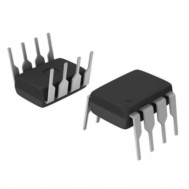
ICGOO电子元器件商城为您提供UC3902N由Texas Instruments设计生产,在icgoo商城现货销售,并且可以通过原厂、代理商等渠道进行代购。 UC3902N价格参考¥18.31-¥34.64。Texas InstrumentsUC3902N封装/规格:PMIC - 电源管理 - 专用, Load Share Controller PMIC 8-PDIP。您可以下载UC3902N参考资料、Datasheet数据手册功能说明书,资料中有UC3902N 详细功能的应用电路图电压和使用方法及教程。
Texas Instruments 的 UC3902N 是一款专用电源管理集成电路(PMIC),主要用于电信和数据通信系统中的热插拔控制。该器件可提供精确的电流限制、过流保护以及负载电流监控功能,适用于需要高可靠性和稳定性的应用场景。

UC3902N 常用于以下场景:

1. 服务器和存储设备:在支持热插拔功能的硬盘或模块中,确保在不关闭系统的情况下安全插入或移除组件。
2. 通信设备:如交换机、路由器等网络设备,用于管理线路卡或模块的供电顺序和保护。
3. 工业控制系统:用于保护关键负载免受过流和短路影响,同时实现平稳启动和负载管理。
4. 冗余电源系统:配合MOSFET和外部电路,实现高效、可靠的电源切换与负载分配。

其主要优势包括低导通电阻、快速响应时间、内置软启动功能以及对负载电流的模拟输出监控,有助于提升系统效率和可靠性。
| 参数 | 数值 |
| 产品目录 | 集成电路 (IC)半导体 |
| 描述 | IC LOAD SHARE CONTROLLER 8-DIP专业电源管理 LOAD SHARE CONTROLLER |
| 产品分类 | |
| 品牌 | Texas Instruments |
| 产品手册 | |
| 产品图片 |
|
| rohs | 符合RoHS无铅 / 符合限制有害物质指令(RoHS)规范要求 |
| 产品系列 | 电源管理 IC,专业电源管理,Texas Instruments UC3902N- |
| 数据手册 | |
| 产品型号 | UC3902N |
| 产品目录页面 | |
| 产品种类 | 专业电源管理 |
| 供应商器件封装 | 8-PDIP |
| 其它名称 | 296-11341-5 |
| 包装 | 管件 |
| 单位重量 | 528.600 mg |
| 商标 | Texas Instruments |
| 安装类型 | 通孔 |
| 安装风格 | Through Hole |
| 封装 | Tube |
| 封装/外壳 | 8-DIP(0.300",7.62mm) |
| 封装/箱体 | PDIP-8 |
| 工作温度 | 0°C ~ 70°C |
| 工作温度范围 | 0 C to + 70 C |
| 工厂包装数量 | 50 |
| 应用 | 负荷分载控制器 |
| 标准包装 | 50 |
| 电压-电源 | 2.7 V ~ 20 V |
| 电流-电源 | 4mA |
| 电源电压 | 2.7 V to 20 V |
| 电源电流 | 6 mA |
| 类型 | Load Share Controllers |
| 系列 | UC3902 |
| 输入电压范围 | 2.7 V to 20 V |
| 输出电流 | 150 uA |
| 配用 | /product-detail/zh/UCC39002EVM/296-19045-ND/863866 |


- 商务部:美国ITC正式对集成电路等产品启动337调查
- 曝三星4nm工艺存在良率问题 高通将骁龙8 Gen1或转产台积电
- 太阳诱电将投资9.5亿元在常州建新厂生产MLCC 预计2023年完工
- 英特尔发布欧洲新工厂建设计划 深化IDM 2.0 战略
- 台积电先进制程称霸业界 有大客户加持明年业绩稳了
- 达到5530亿美元!SIA预计今年全球半导体销售额将创下新高
- 英特尔拟将自动驾驶子公司Mobileye上市 估值或超500亿美元
- 三星加码芯片和SET,合并消费电子和移动部门,撤换高东真等 CEO
- 三星电子宣布重大人事变动 还合并消费电子和移动部门
- 海关总署:前11个月进口集成电路产品价值2.52万亿元 增长14.8%


PDF Datasheet 数据手册内容提取
UC2902 UC3902 SLUS232E − DECEMBER 19, 2002 − REVISED JULY 2011 LOAD SHARE CONTROLLER FEATURES DESCRIPTION (cid:2) 2.7-V to 20-V Operation The UC3902 load share controller is an 8-pin (cid:2) 8-Pin Package device that balances the current drawn from (cid:2) Requires Minimum Number of External independent, paralleled power supplies. Load Components sharing is accomplished by adjusting each (cid:2) supplies’ output current to a level proportional to Compatible with Existing Power Supply the voltage on a share bus. Designs Incorporating Remote Output Voltage Sensin The master power supply, which is automatically (cid:2) Differential Share Bus designated as the supply that regulates to the (cid:2) highest voltage, drives the share bus with a Precision Current Sense Amplifier (40 Gain) voltage proportional to its output current. The (cid:2) UVLO (Undervoltage Lockout) Circuitry UC3902 trims the output voltage of the other (cid:2) User Programmable Share Loop paralleled supplies so that they each support their Compensation share of the load current. Typically, each supply is designed for the same current level although that APPLICATIONS is not necessary for use with the UC3902. By (cid:2) appropriately scaling the current sense resistor, Paralelled Power Supplies supplies with different output current capability can be paralleled with each supply providing the same percentage of their output current capability for a particular load. GND 1 8 VCC BIAS UVLO − SHARE DRIVE AMPLIFIER + 40R R SENSE 2 − 7 SHARE+ + + CURRENT SENSE SHARE SENSE AMPLIFIER AMPLIFIER − 6 SHARE− ERROR AMPLIFIER + ADJ 3 0.6 V 35 mV + − ADJ AMPLIFIER + + 5 COMP − 2.3 V ADJR 4 UDG−01141 PRODUCTION DATA information is current as of publication date. Copyright © 2002 − 2008, Texas Instruments Incorporated Products conform to specifications per the terms of Texas Instruments standard warranty. Production processing does not necessarily include testing of all parameters. www.ti.com 1
UC2902 UC3902 SLUS232E − DECEMBER 19, 2002 − REVISED JULY 2011 DESCRIPTION (continued) A differential line is used for the share bus to maximize noise immunity and accommodate different voltage drops in each power converter’s ground return line. Trimming of each converter’s output voltage is accomplished by injecting a small current into the output voltage sense line, which requires a small resistance (typically 20 Ω to 100 Ω) to be inserted. These devices have limited built-in ESD protection. The leads should be shorted together or the device placed in conductive foam during storage or handling to prevent electrostatic damage to the MOS gates. ABSOLUTE MAXIMUM RATINGS over operating free-air temperature range unless otherwise noted(1) UC2902 UNIT UC3902 VCC, ADJ −0.3 to 20 SENSE −5 to 5 IInnppuutt vvoollttaaggee rraannggee, VVI ADJR, COMP −0.3 to 4 VV SHARE−, SHARE+ −0.3 to 10 SHARE+ −100 mA to 10 mA mA OOuuttppuutt ccuurrrreenntt, IIO ADJ −1 mA to 30 mA mA Operating free-air temperature range, TA −40 to 100 Junction temperature range, TJ −55 to 105 °°CC Storage temperature, Tstg −65 to 150 Lead temperature 1,6 mm (1/16 inch) from case for 10 seconds 300 (1) Stresses beyond those listed under “absolute maximum ratings” may cause permanent damage to the device. These are stress ratings only, and functional operation of the device at these or any other conditions beyond those indicated under “recommended operating conditions” is not implied. Exposure to absolute-maximum-rated conditions for extended periods may affect device reliability. Voltages are with respect to GND. Currents are positive into, and negative out of the specified terminal. 2 www.ti.com
UC2902 UC3902 SLUS232E − DECEMBER 19, 2002 − REVISED JULY 2011 ELECTRICAL CHARACTERISTICS TJ = –40°C to 105°C, (unless otherwise noted) PARAMETER TEST CONDITIONS MIN TYP MAX UNIT Power SUPPLY SUPPLY CURRENT SHARE+ = 1 V, SENSE = 0 V 4 6 IICC SSuuppppllyy ccuurrrreenntt VCC = 20 V 6 10 mmAA UNDERVOLTAGE LOCKOUT VCC Startup voltage SHARE+ = 0.2 V, SENSE = 0 V, COMP = 1 V 2.3 2.5 2.7 V Hysteresis SHARE+ = 0.2 V, SENSE = 0 V, COMP = 1 V 60 100 140 mV CURRENT SENSE AMPLIFIER VIO Input offset voltage 0.1 V ≤ V(SHARE+) ≤ 1.1 V −2.5 −0.5 1.5 mV SENSE to SHARE gain 0.1 V ≤ V(SHARE+) ≤ 1.1 V −41 −40 −39 V RIN Input resistance 0.6 1 1.5 V SHARE DRIVE AMPLIFIER VCC = 2.5 V V(SENSE) = −50 mV 1.2 1.4 I(SHARE+) = −1 mA VOH HSSHHigAAh-RRleEEv++el output voltage, VI(SCHCA =R E1+2) V= −1 mA V(SENSE) = −250 mV 9.6 10.0 10.4 V VCC = 20 V V(SENSE) = −250 mV 9.6 10.0 10.4 I(SHARE+) = −1 mA VCC = 2.5 V V(SENSE) = 10 mV 20 50 I(SHARE+) = −1 mA VOL Low-level output voltage, SHARE+ VI(SCHCA =R E1+2) V= −1 mA V(SENSE) = 10 mV 20 50 mmVV VCC = 20 V V(SENSE) = 10 mV 20 50 I(SHARE+) = −1 mA VO Output voltage, SHARE+ V(S(SHEANRSEE)+ = t o0 GmNVD, ) R(SHARE+) = 200 Ω 20 40 CMRR Common mode rejection ratio 0 V ≤ V(SHARE−) ≤ 1 V, 50 90 dB SENSE used as input to amplifier Load regulation Load on SHARE+, 1 mA ≤ ILOAD ≤ −20 mA 0 20 mV V(SENSE) = −25 mV ISC Short circuit current V(SHARE+) = 0 V, V(SENSE) = −25 mV −85 −50 −20 mA VR((SSEHNASREE)+ =) = 1 02 0m0V Ω t o ( S−H90A RmEV+ s ttoe pGND) 0.12 0.26 0.38 SSlleeww rraattee VV//μss RV((SSEHNASREE)+ =) = − 29000 m ΩV t(oS H10A RmEV+ s ttoe pGND) 0.12 0.26 0.38 www.ti.com 3
UC2902 UC3902 SLUS232E − DECEMBER 19, 2002 − REVISED JULY 2011 ELECTRICAL CHARACTERISTICS (continued) TJ = –40°C to 105°C, (unless otherwise noted) PARAMETER TEST CONDITIONS MIN TYP MAX UNIT SHARE SENSE AMPLIFIER V(SHARE+) = 1 V, V(SHARE−) = GND 8 15 V(SENSE) = 10 mV RRIN IInnppuutt iimmppeeddaannccee R(SHARE+) = 200 Ω (SHARE+ to GND) 8 15 kkΩΩ V(SHARE−) = 1 V, V(SENSE) = 10 mV V(SHARE) Threshold voltage V(SENSE) = 0 V 41 70 100 mV CMRR Common mode rejection ratio 0 V ≤ V(SHARE−) ≤ 1 V, V(SENSE) = −2.5 mV 50 60 V(SENSE) = −2.5 mV, 5 nF capacitor from COMP to GND, 50 68 DDEESSCCRRIIPPTTIIOONN ffrroomm SSHHAARREE++ ttoo 1 kΩ resistor from ADJR to GND ddBB AAVVOOLL ADJR V(SENSE) = −2.5 mV, 5 nF capacitor from COMP to GND, 50 66 150 Ω resistor from ADJR to GND V(SHARE+) = 0 mV to 10 V step through a 200-Ω Slew rate resistor, R(COMP) = 500 Ω, 0.2 0.5 0.8 V/μs V(SENSE) = 10 mV, VCC = 10 V ERROR AMPLIFIER Transconductance, SHARE+ to gM COMP 200-Ω resistor SHARE+ to GND 3.0 4.5 6.0 mS IOH High-level output current VV((SCEONMSPE) )= = 1−.150 V m, V SHARE+ ≥ 300 mV −450 −325 −200 μAA 200-Ω resistor SHARE+ to GND, IOL Low-level output current V(COMP) = 1.5 V, V(SENSE) = 10 mV 80 150 250 VIO Input offset voltage 15 35 65 mV ΔΔVVI(OSE/NSE) 1−-2k.Ω5 mreVs i≤s tVor( SAEDNJSRE) t≤o −G2N5D mV −6 0 6 mV/V ADJ AMPLIFIER 200-Ω resistor SHARE+ to GND, ADJR low voltage −1 0 1 mV V(SENSE) = 10 mV ADJR high voltage V(SENSE) = 10 mV, V(SHARE+) = 1 V 1.4 1.8 2.1 V I(ADJR) = −0.5 mA, V(ADJ) = 2.5 V, 0.96 0.99 1.02 V(SENSE) = 10 mV, V(SHARE+) = 1 V I(ADJR) = −0.5 mA, V(ADJ) = 20 V, 0.96 0.99 1.02 V(SENSE) = 10 mV, V(SHARE+) = 1 V CCuurrrreenntt ggaaiinn AADDJJRR ttoo AADDJJ AA//AA I(ADJR) = −10 mA, V(ADJ) = 2.5 V, 0.96 0.99 1.02 V(SENSE) = 10 mV, V(SHARE+) = 1 V I(ADJR) = −10 mA, V(ADJ) = 20 V, 0.96 0.99 1.02 V(SENSE) = 10 mV, V(SHARE+) = 1 V 4 www.ti.com
UC2902 UC3902 SLUS232E − DECEMBER 19, 2002 − REVISED JULY 2011 ORDERING INFORMATION TA PACKAGE(2) PART NUMBER SOIC (D) UC2902D −4400°°CC ttoo 8855°°CC Plastic DIP (N) UC2902N SOIC (D) UC3902D 00°°CC ttoo 7700°°CC Plastic DIP (N) UC3902N (2) The D package is also available taped and reeled. Add an R suffix to the device type (i.e., bq24901DR) for quantities of 3,000 devices per reel. D PACKAGE N PACKAGE (TOP VIEW) (TOP VIEW) GND 1 8 VCC GND 1 8 VCC SENSE 2 7 SHARE+ SENSE 2 7 SHARE+ ADJ 3 6 SHARE− ADJ 3 6 SHARE− ADJR 4 5 COMP ADJR 4 5 COMP TERMINAL FUNCTIONS TERMINAL II//OO DDEESSCCRRIIPPTTIIOONN NAME NO. ADJ 3 I Current output of the adjust amplifier circuit (NPN collector) ADJR 4 O Current adjust amplifier range set (NPN emitter) COMP 5 I/O Output of the error amplifier, input of the adjust amplifier GND 1 − Local power supply return and signal ground SENSE 2 I Inverting input of the current sense amplifier SHARE+ 7 I/O Positive input from share bus or drive-to-share bus SHARE− 6 I Reference for SHARE+ pin VCC 8 I Local power supply (positive) www.ti.com 5
UC2902 UC3902 SLUS232E − DECEMBER 19, 2002 − REVISED JULY 2011 APPLICATION INFORMATION The values of five passive components must be determined to configure the UC3902 load share controller. The output and return lines of each converter are connected together at the load, with current sense resistor R SENSE inserted in each negative return line. Another resistor, R , is also inserted in each positive remote sense line. ADJ The differential share bus terminals (SHARE+ and SHARE−) of each UC3902 are connected together respectively, and the SHARE− node is also connected to the system ground. A typical application is illustrated in Figure 1. The load share controller design can be executed by following the next few steps: Step 1. V R (cid:2) SHARE(max) SENSE A (cid:3)I CSA O(max) (1) (cid:2) where A is 40, the gain of the current sense amplifier CSA At full load, the voltage drop across the R resistor is I × R . Taking into account the gain of the SENSE O(max) SENSE current sense amplifier, the voltage at full load on the current share bus, A (cid:3)I V (cid:2) CSA O(max) SHARE(max) R SENSE (2) This voltage must stay 1.5-V below V or below 10 V whichever is smaller. V represents an upper limit CC SHARE but the designer should select the full scale share bus voltage keeping in mind that every volt on the load share bus increases the master controller’s supply current by approximately 100 μA times the number of slave units connected parallel. Step 2. V R (cid:2) ADJ(max) G I ADJ(max) (3) Care must be taken to ensure that I is low enough so that both the drive current and power dissipation ADJ(max) are within the device’s capability. For most applications, an I current between 5 mA and 10 mA is ADJ(max) acceptable. In a typical application, a 360-Ω R resistor from the ADJR pin to ground sets I to G ADJ(max) approximately 5 mA. Step 3. (cid:5) (cid:6) (cid:2)V (cid:4) I (cid:3)R O(max) O(max) SENSE R (cid:2) ADJ I ADJ(max) (4) R must be low enough to not affect the normal operation of the converter’s voltage feedback loop. Typical ADJ R values are between 20 Ω to100 Ω depending on V , ΔV and the selected I value. ADJ O O(max) ADJ(max) Step 4. g R R (cid:5) (cid:6) C (cid:2) M (cid:3) ADJ(cid:3) SENSE(cid:3)A (cid:3)A f C 2(cid:3)(cid:3)f R R CSA PWR C C G LOAD (5) 6 www.ti.com
UC2902 UC3902 SLUS232E − DECEMBER 19, 2002 − REVISED JULY 2011 The share loop compensation capacitor, C is calculated to produce the desired share loop unity gain crossover C frequency, f . The share loop error amplifier’s transconductance, g is nominally 4.5 ms. The values of the C M resistors are already known. Typically, f is set to at least one order of magnitude below the converter’s closed C loop bandwidth. The load share circuit is primarily intended to compensate for each converter’s initial output voltage tolerance and temperature drift, not for differences in their transient response. The term A is the PWR(fc) gain of the power supply measured at the desired share loop crossover frequency, f . This gain can be C measured by injecting the measurement signal between the positive output and the positive sense terminal of the power supply. Step 5. R (cid:2) 1 C 2(cid:3)(cid:3)f (cid:3)C C C (6) A resistor in series with C is required to boost the phase margin of the load share loop. The zero is placed at C the load share loop crossover frequency, f . C When the system is powered up, the converter with the highest output voltage tends to source the most current and take control of the share bus. The other converters increase their output voltages until their output currents are proportional to the share bus voltage minus 50 mV. The converter which in functioning as the master may change due to warmup drift and differences in load and line transient response of each converter. ADDITIONAL INFORMATION Please refer to the following topic for additional application information. 1. Application Note U−163, (TI Literature No. SLUA128) The UC3902 Load Share Controller and Its Performance in Distributed Power Systems by Laszlo Balogh www.ti.com 7
PACKAGE MATERIALS INFORMATION www.ti.com 28-Jul-2011 TAPE AND REEL INFORMATION *Alldimensionsarenominal Device Package Package Pins SPQ Reel Reel A0 B0 K0 P1 W Pin1 Type Drawing Diameter Width (mm) (mm) (mm) (mm) (mm) Quadrant (mm) W1(mm) UC2902DTR SOIC D 8 2500 330.0 12.4 6.4 5.2 2.1 8.0 12.0 Q1 UC3902DTR SOIC D 8 2500 330.0 12.4 6.4 5.2 2.1 8.0 12.0 Q1 PackMaterials-Page1
PACKAGE MATERIALS INFORMATION www.ti.com 28-Jul-2011 *Alldimensionsarenominal Device PackageType PackageDrawing Pins SPQ Length(mm) Width(mm) Height(mm) UC2902DTR SOIC D 8 2500 340.5 338.1 20.6 UC3902DTR SOIC D 8 2500 340.5 338.1 20.6 PackMaterials-Page2
IMPORTANTNOTICE TexasInstrumentsIncorporatedanditssubsidiaries(TI)reservetherighttomakecorrections,modifications,enhancements,improvements, andotherchangestoitsproductsandservicesatanytimeandtodiscontinueanyproductorservicewithoutnotice.Customersshould obtainthelatestrelevantinformationbeforeplacingordersandshouldverifythatsuchinformationiscurrentandcomplete.Allproductsare soldsubjecttoTI’stermsandconditionsofsalesuppliedatthetimeoforderacknowledgment. TIwarrantsperformanceofitshardwareproductstothespecificationsapplicableatthetimeofsaleinaccordancewithTI’sstandard warranty.TestingandotherqualitycontroltechniquesareusedtotheextentTIdeemsnecessarytosupportthiswarranty.Exceptwhere mandatedbygovernmentrequirements,testingofallparametersofeachproductisnotnecessarilyperformed. TIassumesnoliabilityforapplicationsassistanceorcustomerproductdesign.Customersareresponsiblefortheirproductsand applicationsusingTIcomponents.Tominimizetherisksassociatedwithcustomerproductsandapplications,customersshouldprovide adequatedesignandoperatingsafeguards. TIdoesnotwarrantorrepresentthatanylicense,eitherexpressorimplied,isgrantedunderanyTIpatentright,copyright,maskworkright, orotherTIintellectualpropertyrightrelatingtoanycombination,machine,orprocessinwhichTIproductsorservicesareused.Information publishedbyTIregardingthird-partyproductsorservicesdoesnotconstitutealicensefromTItousesuchproductsorservicesora warrantyorendorsementthereof.Useofsuchinformationmayrequirealicensefromathirdpartyunderthepatentsorotherintellectual propertyofthethirdparty,oralicensefromTIunderthepatentsorotherintellectualpropertyofTI. ReproductionofTIinformationinTIdatabooksordatasheetsispermissibleonlyifreproductioniswithoutalterationandisaccompanied byallassociatedwarranties,conditions,limitations,andnotices.Reproductionofthisinformationwithalterationisanunfairanddeceptive businesspractice.TIisnotresponsibleorliableforsuchaltereddocumentation.Informationofthirdpartiesmaybesubjecttoadditional restrictions. ResaleofTIproductsorserviceswithstatementsdifferentfromorbeyondtheparametersstatedbyTIforthatproductorservicevoidsall expressandanyimpliedwarrantiesfortheassociatedTIproductorserviceandisanunfairanddeceptivebusinesspractice.TIisnot responsibleorliableforanysuchstatements. TIproductsarenotauthorizedforuseinsafety-criticalapplications(suchaslifesupport)whereafailureoftheTIproductwouldreasonably beexpectedtocauseseverepersonalinjuryordeath,unlessofficersofthepartieshaveexecutedanagreementspecificallygoverning suchuse.Buyersrepresentthattheyhaveallnecessaryexpertiseinthesafetyandregulatoryramificationsoftheirapplications,and acknowledgeandagreethattheyaresolelyresponsibleforalllegal,regulatoryandsafety-relatedrequirementsconcerningtheirproducts andanyuseofTIproductsinsuchsafety-criticalapplications,notwithstandinganyapplications-relatedinformationorsupportthatmaybe providedbyTI.Further,BuyersmustfullyindemnifyTIanditsrepresentativesagainstanydamagesarisingoutoftheuseofTIproductsin suchsafety-criticalapplications. TIproductsareneitherdesignednorintendedforuseinmilitary/aerospaceapplicationsorenvironmentsunlesstheTIproductsare specificallydesignatedbyTIasmilitary-gradeor"enhancedplastic."OnlyproductsdesignatedbyTIasmilitary-grademeetmilitary specifications.BuyersacknowledgeandagreethatanysuchuseofTIproductswhichTIhasnotdesignatedasmilitary-gradeissolelyat theBuyer'srisk,andthattheyaresolelyresponsibleforcompliancewithalllegalandregulatoryrequirementsinconnectionwithsuchuse. TIproductsareneitherdesignednorintendedforuseinautomotiveapplicationsorenvironmentsunlessthespecificTIproductsare designatedbyTIascompliantwithISO/TS16949requirements.Buyersacknowledgeandagreethat,iftheyuseanynon-designated productsinautomotiveapplications,TIwillnotberesponsibleforanyfailuretomeetsuchrequirements. FollowingareURLswhereyoucanobtaininformationonotherTexasInstrumentsproductsandapplicationsolutions: Products Applications Audio www.ti.com/audio CommunicationsandTelecom www.ti.com/communications Amplifiers amplifier.ti.com ComputersandPeripherals www.ti.com/computers DataConverters dataconverter.ti.com ConsumerElectronics www.ti.com/consumer-apps DLP®Products www.dlp.com EnergyandLighting www.ti.com/energy DSP dsp.ti.com Industrial www.ti.com/industrial ClocksandTimers www.ti.com/clocks Medical www.ti.com/medical Interface interface.ti.com Security www.ti.com/security Logic logic.ti.com Space,AvionicsandDefense www.ti.com/space-avionics-defense PowerMgmt power.ti.com Transportationand www.ti.com/automotive Automotive Microcontrollers microcontroller.ti.com VideoandImaging www.ti.com/video RFID www.ti-rfid.com Wireless www.ti.com/wireless-apps RF/IFandZigBee®Solutions www.ti.com/lprf TIE2ECommunityHomePage e2e.ti.com MailingAddress:TexasInstruments,PostOfficeBox655303,Dallas,Texas75265 Copyright©2011,TexasInstrumentsIncorporated