ICGOO在线商城 > 集成电路(IC) > PMIC - 电源管理 - 专用 > LM25066APSQE/NOPB

 Datasheet下载
- 型号: LM25066APSQE/NOPB
- 制造商: Texas Instruments
- 库位|库存: xxxx|xxxx
- 要求:
| 数量阶梯 | 香港交货 | 国内含税 |
| +xxxx | $xxxx | ¥xxxx |
查看当月历史价格
查看今年历史价格
LM25066APSQE/NOPB产品简介:
ICGOO电子元器件商城为您提供LM25066APSQE/NOPB由Texas Instruments设计生产,在icgoo商城现货销售,并且可以通过原厂、代理商等渠道进行代购。 LM25066APSQE/NOPB价格参考。Texas InstrumentsLM25066APSQE/NOPB封装/规格:PMIC - 电源管理 - 专用, Base Station-Networking Line Cards, Servers PMIC 24-WQFN (4x5)。您可以下载LM25066APSQE/NOPB参考资料、Datasheet数据手册功能说明书,资料中有LM25066APSQE/NOPB 详细功能的应用电路图电压和使用方法及教程。
LM25066APSQE/NOPB 是由德州仪器(Texas Instruments)生产的一款专用电源管理集成电路(PMIC),属于 LM25066 系列。该器件专为需要高效、紧凑和可靠电源解决方案的应用场景而设计,主要应用于以下领域:

1. 工业设备
   - 适用于工业自动化系统中的电源管理,例如 PLC(可编程逻辑控制器)、数据采集系统和传感器接口。
   - 提供稳定的电源输出,支持高可靠性工业应用。

2. 通信设备
   - 用于路由器、交换机和基站等通信设备的电源模块。
   - 支持低噪声和高效率的电源转换,满足通信设备对信号完整性的要求。

3. 医疗电子
   - 在便携式医疗设备(如血压计、血糖仪)或固定式医疗设备(如监护仪、超声设备)中提供可靠的电源供应。
   - 具备小尺寸和低功耗特性,适合对空间和能效要求较高的医疗应用。

4. 汽车电子
   - 应用于车载信息娱乐系统、ADAS(高级驾驶辅助系统)和车身控制模块。
   - 能够承受汽车环境中的宽温度范围和电压波动。

5. 消费电子
   - 用于数字电视、机顶盒和游戏主机等消费电子产品,提供高效的电源转换。
   - 支持快速动态响应,确保设备在负载变化时保持稳定运行。

LM25066APSQE/NOPB 的特点包括高集成度、宽输入电压范围、低静态电流和多种保护功能(如过流保护、过温保护)。这些特性使其成为需要高性能电源管理的各类应用的理想选择。
| 参数 | 数值 |
| 产品目录 | 集成电路 (IC)半导体 |
| 描述 | IC CTLR PM HOTSWAP 24-LLP热交换电压控制器 System Pwr Mgmt & Protect IC w/ PMBus |
| 产品分类 | |
| 品牌 | Texas Instruments |
| 产品手册 | http://www.ti.com/lit/gpn/lm25066a |
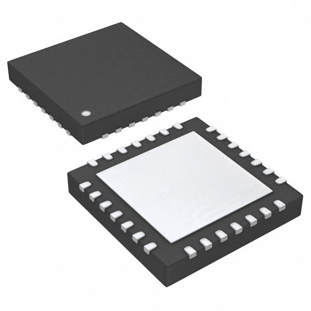
| 产品图片 |
|
| rohs | 符合RoHS无铅 / 符合限制有害物质指令(RoHS)规范要求 |
| 产品系列 | 电源管理 IC,热交换电压控制器,Texas Instruments LM25066APSQE/NOPB- |
| 数据手册 | |
| 产品型号 | LM25066APSQE/NOPB |
| 产品 | Controllers & Switches |
| 产品种类 | 热交换电压控制器 |
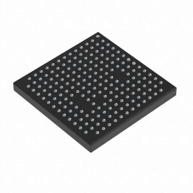
| 供应商器件封装 | 24-WQFN (4x5) |
| 其它名称 | *LM25066APSQE/NOPB |
| 包装 | 剪切带 (CT) |
| 商标 | Texas Instruments |
| 安装类型 | 表面贴装 |
| 安装风格 | SMD/SMT |
| 封装 | Reel |
| 封装/外壳 | 24-WFQFN 裸露焊盘 |
| 封装/箱体 | WQFN-24 |
| 工作温度 | -40°C ~ 85°C |
| 工作温度范围 | - 40 C to + 125 C |
| 工厂包装数量 | 250 |
| 应用 | 基站网络线路卡,服务器 |
| 标准包装 | 1 |
| 电压-电源 | 2.9 V ~ 17 V |
| 电流-电源 | 5.8mA |
| 电流限制 | 46 mV |
| 电源电压-最大 | 17 V |
| 电源电压-最小 | 2.9 V |
| 电源电流 | 5.8 mA |
| 系列 | LM25066A |


PDF Datasheet 数据手册内容提取
Product Sample & Technical Tools & Support & Folder Buy Documents Software Community LM25066A SNVS700G–DECEMBER2010–REVISEDOCTOBER2016 LM25066A System Power Management and Protection IC With PMBus™ 1 Features 2 Applications • InputVoltageRange:2.9Vto17V • ServerBackplaneSystems 1 • I2C/SMBusInterfaceandPMBusCompliant • BasestationPowerDistributionSystems CommandStructure • SolidStateCircuitBreakers • Programmable25-mVor46-mVCurrentLimit Threshold 3 Description • ConfigurableCircuitBreakerProtectionforHard The LM25066A combines a high-performance hot- Shorts swapcontrollerwithaPMBus™compliantSMBus/I2C interface to accurately measure, protect and control • ConfigurableUndervoltageandOvervoltage the electrical operating conditions of computing and LockoutsWithHysteresis storage blades connected to a backplane power bus. • RemoteTemperatureSensingWith The LM25066A continuously supplies real-time ProgrammableWarningandShutdown power, voltage, current, temperature and fault data to Thresholds the system management host via the SMBus interface. • DetectionandNotificationofDamagedMOSFET Condition The LM25066A control block includes a unique hot- • RealTimeMonitoringofV ,V ,I ,P ,V swap architecture that provides current and power IN OUT IN IN AUX With12-BitResolutionand1-kHzSamplingRate limiting to protect sensitive circuitry during insertion of boards into a live system backplane, or any other hot • CurrentMeasurementAccuracy:±1%Over power source. A fast acting circuit breaker prevents Temperature damage in the event of a short circuit on the output. • PowerMeasurementAccuracy:±2%Over The input undervoltage and overvoltage levels and Temperature hysteresis are configurable, as well as the insertion delay time and fault detection time. A temperature • TrueInputPowerMeasurementUsing monitoring block on the LM25066A interfaces with a SimultaneousSamplingofV andI Accurately IN IN low-cost external diode for monitoring the AveragesDynamicPowerReadings temperature of the external MOSFET or other • AveragingofVIN,IIN,PIN,andVOUTOver thermally sensitive components. The POWER GOOD ProgrammableIntervalRangingfrom0.001to4 output provides a fast indicator when the input and/or Seconds output voltages are outside their programmed range. • ProgrammableWARNandFAULTThresholds LM25066A current measurement accuracy is ±1% overtemperature. withSMBANotification • BlackBoxCaptureofTelemetryMeasurements DeviceInformation(1) andDeviceStatusTriggeredbyWARNorFAULT PARTNUMBER PACKAGE BODYSIZE(NOM) Condition LN25066A WQFN(24) 5.00mm×4.00mm • 24-LeadWQFNPackage (1) For all available packages, see the orderable addendum at theendofthedatasheet. TypicalApplicationSchematic Only required when FET VIN RSNS Q2 Vgs rating is < +/-20V VOUT Q1 CIN Z1 D3 D2 COUT Only required when SENSE GATE OUTDIODE RFB1 using dv/dt start-up R1 R3 VIN FB VDD D1 RFB2 UVLO/EN 10k(cid:159) R2 R4 OVLO LM25066A AAPDDGRRD12 1k(cid:159) Q3 Cdv/dt GND ADR0 CL SMBA RETRY InSteMrfBacues SSCDLA VAUX A(0uVx i"lla r1y. 1A6DVC) Input VDD VREF PWR TIMER 1 PF 1 PF RPWR CTIMER Copyright © 2016, Texas Instruments Incorporated 1 An IMPORTANT NOTICE at the end of this data sheet addresses availability, warranty, changes, use in safety-critical applications, intellectualpropertymattersandotherimportantdisclaimers.PRODUCTIONDATA.
LM25066A SNVS700G–DECEMBER2010–REVISEDOCTOBER2016 www.ti.com Table of Contents 1 Features.................................................................. 1 8.3 FeatureDescription.................................................17 2 Applications........................................................... 1 8.4 DeviceFunctionalModes........................................20 3 Description............................................................. 1 8.5 RegisterMaps ........................................................24 4 RevisionHistory..................................................... 2 9 ApplicationandImplementation........................ 43 9.1 ApplicationInformation............................................43 5 Description(continued)......................................... 3 9.2 TypicalApplication .................................................43 6 PinConfigurationandFunctions......................... 3 10 PowerSupplyRecommendations..................... 57 7 Specifications......................................................... 5 11 Layout................................................................... 57 7.1 AbsoluteMaximumRatings .....................................5 11.1 LayoutGuidelines.................................................57 7.2 ESDRatings ............................................................5 11.2 LayoutExample....................................................58 7.3 RecommendedOperatingConditions.......................5 12 DeviceandDocumentationSupport................. 59 7.4 ThermalInformation..................................................5 7.5 ElectricalCharacteristics...........................................6 12.1 DeviceSupport......................................................59 7.6 TimingRequirements:SMBusCommunications......9 12.2 ReceivingNotificationofDocumentationUpdates59 7.7 SwitchingCharacteristics..........................................9 12.3 CommunityResources..........................................59 7.8 TypicalCharacteristics............................................11 12.4 Trademarks...........................................................59 12.5 ElectrostaticDischargeCaution............................59 8 DetailedDescription............................................ 16 12.6 Glossary................................................................59 8.1 Overview.................................................................16 13 Mechanical,Packaging,andOrderable 8.2 FunctionalBlockDiagram.......................................17 Information........................................................... 59 4 Revision History NOTE:Pagenumbersforpreviousrevisionsmaydifferfrompagenumbersinthecurrentversion. ChangesfromRevisionF(February2013)toRevisionG Page • AddedFeatureDescriptionsection,DeviceFunctionalModes,ApplicationandImplementationsection,Power SupplyRecommendationssection,DeviceandDocumentationSupportsection,andMechanical,Packaging,and OrderableInformation............................................................................................................................................................. 1 ChangesfromRevisionE(February2013)toRevisionF Page • ChangedlayoutofNationalSemiconductorDataSheettoTIformat ................................................................................... 1 2 SubmitDocumentationFeedback Copyright©2010–2016,TexasInstrumentsIncorporated ProductFolderLinks:LM25066A
LM25066A www.ti.com SNVS700G–DECEMBER2010–REVISEDOCTOBER2016 5 Description (continued) The LM25066A monitoring block computes both the real-time and average values of subsystem operating parameters (V , I , P , V ) as well as the peak power. Accurate power averaging is accomplished by IN IN IN OUT averaging the product of the input voltage and current. A black box (Telemetry/Fault Snapshot) function captures andstorestelemetrydataanddevicestatusintheeventofawarningorafault. 6 Pin Configuration and Functions NHZPackage 24-PinWQFN TopView N SDA GND OVLO UVLO/E VIN SENSE GATE SCL OUT SMBA PGD Exposed VREF PWR Pad DIODE TIMER 24 VAUX RETRY ADR2 ADR1 ADR0 VDD CL CB FB 1 5x4 mm WQFN 24L Soldertheexposedpadtoground. PinFunctions PIN TYPE DESCRIPTION NO. NAME 1 ADR2 SMBUSaddressline2 3-stateaddressline.ShouldbeconnectedtoGND,VDD,orleftfloating. 2 ADR1 SMBUSaddressline1 3-stateaddressline.ShouldbeconnectedtoGND,VDD,orleftfloating. 3 ADR0 SMBUSaddressline0 3-stateaddressline.ShouldbeconnectedtoGND,VDD,orleftfloating. Internalsub-regulator Internallysub-regulated4.5-Vbiassupply.Connecta1-µFcapacitoronthispintoground 4 VDD output forbypassing. ConnectthispintoGNDtosetthenominalovercurrentthresholdat25mV.Connecting 5 CL Currentlimitrange CLtoVDDsetstheovercurrentthresholdtobe46mV. Thispinsetsthecircuitbreakerprotectionpointinrelationtotheovercurrenttrippoint. WhenconnectedtoGND,thispinsetsthecircuitbreakerpointtobe1.8timesthe 6 CB Circuitbreakerrange overcurrentthreshold.ConnectingthispintoVDDsetsthecircuitbreakertrippointtobe 3.6timestheovercurrentthreshold. AnexternalresistordividerfromOUTsetstheoutputvoltageatwhichthePGDpin 7 FB PowerGoodfeedback switches.Thethresholdatthepinis1.167V.Aninternal24-µAcurrentsourceprovides hysteresis. Thispinconfiguresthepowerupfaultretrybehavior.Whenthispinisgrounded,the 8 RETRY Faultretryinput devicecontinuallytriestoengagepowerduringafault.IfthepinisconnectedtoVDD,the devicewilllatchoffduringafault. Anexternalcapacitorconnectedtothispinsetstheinsertiontimedelay,faulttimeout 9 TIMER Timingcapacitor periodandrestarttiming. Anexternalresistorconnectedtothispin,inconjunctionwiththecurrentsenseresistor 10 PWR Powerlimitset (R ),setsthemaximumpowerdissipationallowedintheexternalseriespassMOSFET. S Copyright©2010–2016,TexasInstrumentsIncorporated SubmitDocumentationFeedback 3 ProductFolderLinks:LM25066A
LM25066A SNVS700G–DECEMBER2010–REVISEDOCTOBER2016 www.ti.com PinFunctions(continued) PIN TYPE DESCRIPTION NO. NAME Anopendrainoutput.ThisoutputishighwhenthevoltageattheFBpinisabove1.167V andtheinputsupplyiswithinitsundervoltageandovervoltagethresholds.Connect 11 PGD PowerGoodindicator throughapullupresistortotheoutputrail(externalMOSFETsource)oranyothervoltage tobemonitored. Connecttotheoutputrail(externalMOSFETsource).Internallyusedtodeterminethe 12 OUT Outputfeedback MOSFETV voltageforpowerlimiting,andtomonitortheoutputvoltage. DS 13 GATE Gatedriveoutput ConnecttotheexternalMOSFET'sgate. Thevoltageacrossthecurrentsenseresistor(R )ismeasuredfromVINtothispin.Ifthe S 14 SENSE Currentsenseinput voltageacrossR reachesovercurrentthreshold,theloadcurrentislimitedandthefault S timeractivates. Asmallceramicbypasscapacitorclosetothispinisrecommendedtosuppresstransients 15 VIN Positivesupplyinput whichoccurwhentheloadcurrentisswitchedoff. Anexternalresistordividerfromthesysteminputvoltagesetstheundervoltageturnon 16 UVLO/EN Under-voltagelockout threshold.Aninternal23-µAcurrentsourceprovideshysteresis.Theenablethresholdat thepinis1.16V.Thispincanalsobeusedforremoteshutdowncontrol. Anexternalresistordividerfromthesysteminputvoltagesetstheovervoltageturnoff 17 OVLO Over-voltagelockout threshold.Aninternal23-µAcurrentsourceprovideshysteresis.Thedisablethresholdat thepinis1.16V. 18 GND Circuitground 19 SDA SMBusdatapin DatapinforSMBus. 20 SCL SMBusclock ClockpinforSMBus. 21 SMBA SMBusalertline AlertpinforSMBus,activelow. Internallygeneratedprecision2.73-Vreferenceusedforanalogtodigitalconversion. 22 VREF InternalReference Connecta1-µFcapacitoronthispintogroundforbypassing. 23 DIODE Externaldiode Connectthistoadiode-configuredNPNtransistorfortemperaturemonitoring. 24 VAUX Auxiliaryvoltageinput Auxiliarypinallowsvoltagetelemetryfromanexternalsource.Fullscaleinputof1.16V. Exposed ExposedpadofWQFN Nointernalelectricalconnections.Soldertothegroundplanetoreducethermal Pad Pad package resistance. 4 SubmitDocumentationFeedback Copyright©2010–2016,TexasInstrumentsIncorporated ProductFolderLinks:LM25066A
LM25066A www.ti.com SNVS700G–DECEMBER2010–REVISEDOCTOBER2016 7 Specifications 7.1 Absolute Maximum Ratings overoperatingfree-airtemperaturerange(unlessotherwisenoted) (1) MIN MAX UNIT VIN,SENSEtoGND (2) –0.3 24 V GATE,FB,UVLO/EN,OVLO,PGDtoGND (2) –0.3 20 V OUTtoGND –1 20 V Inputvoltage SCL,SDA,SMBA,CL,CB,ADR0,ADR1,ADR2,VDD,VAUX, –0.3 6 V DIODE,RETRYtoGND VINtoSENSE –0.3 0.3 V JunctionTemperature,T 150 °C J Storagetemperature,T –65 150 °C stg (1) StressesbeyondthoselistedunderAbsoluteMaximumRatingsmaycausepermanentdamagetothedevice.Thesearestressratings only,whichdonotimplyfunctionaloperationofthedeviceattheseoranyotherconditionsbeyondthoseindicatedunderRecommended OperatingConditions.Exposuretoabsolute-maximum-ratedconditionsforextendedperiodsmayaffectdevicereliability. (2) TheGATEpinvoltageistypically7.5VaboveVINwhentheLM25066Aisenabled.ThereforetheAbsoluteMaximumRatingof24Vfor VINandSENSEapplyonlywhentheLM25066AisdisabledorforamomentarysurgetothatvoltagesincetheAbsoluteMaximum RatingoftheGATEpinis20V. 7.2 ESD Ratings VALUE UNIT Human-bodymodel(HBM) (1) ±2000 V Electrostaticdischarge V (ESD) Charged-devicemodel(CDM),perJEDECspecificationJESD22-C101(2) ±500 (1) Thehumanbodymodelisa100-pFcapacitordischargedthrougha1.5kΩresistorintoeachpin. (2) JEDECdocumentJEP157statesthat250-VCDMallowssafemanufacturingwithastandardESDcontrolprocess. 7.3 Recommended Operating Conditions overoperatingfree-airtemperaturerange(unlessotherwisenoted) MIN NOM MAX UNIT VIN,SENSE,OUTvoltage 2.9 17 V VDD 2.9 5.5 V Junctiontemperature,T –40 125 °C J 7.4 Thermal Information LM25066A THERMALMETRIC(1) NHZ(WQFN) UNIT 24PINS R Junction-to-ambientthermalresistance 34.1 °C/W θJA R Junction-to-case(top)thermalresistance 28.9 °C/W θJC(top) R Junction-to-boardthermalresistance 13.4 °C/W θJB ψ Junction-to-topcharacterizationparameter 0.3 °C/W JT ψ Junction-to-boardcharacterizationparameter 13.5 °C/W JB R Junction-to-case(bottom)thermalresistance 3.6 °C/W θJC(bot) (1) Formoreinformationabouttraditionalandnewthermalmetrics,seetheSemiconductorandICPackageThermalMetricsapplication report. Copyright©2010–2016,TexasInstrumentsIncorporated SubmitDocumentationFeedback 5 ProductFolderLinks:LM25066A
LM25066A SNVS700G–DECEMBER2010–REVISEDOCTOBER2016 www.ti.com 7.5 Electrical Characteristics TypicallimitsareforT =25°C,andminimumandmaximumlimitsapplyovertheoperatingjunctiontemperaturerange J (–40°Cto85°C).MinimumandMaximumlimitsarespecifiedthroughtest,design,orstatisticalcorrelation.Typicalvalues representthemostlikelyparametricnormatT =25°C,andareprovidedforreferencepurposesonly.Unlessotherwise J statedthefollowingconditionsapply:VIN=12V.(1)(2) PARAMETER TESTCONDITIONS MIN TYP MAX UNIT INPUT(VINPIN) I Inputcurrent,enabled UVLO=2VandOVLO=0.7V 5.8 8 mA IN-EN POR PoweronresetthresholdatVIN VINincreasing 2.6 2.8 V POR POR hysteresis VINdecreasing 150 mV HYS EN VDDREGULATOR(VDDPIN) I =5mA,VIN=12V 4.3 4.5 4.7 V VDD V DD I =5mA,VIN=4.5V 3.5 3.9 4.3 V VDD V VDDcurrentlimit 25 45 mA DDILIM UVLO/EN,OVLOPINS UVLO UVLOthreshold V Falling 1.147 1.16 1.173 V TH UVLO UVLO UVLOhysteresiscurrent UVLO=1V 18 23 28 µA HYS DelaytoGATEhigh 8 UVLO UVLOdelay µs DEL DelaytoGATElow 20 UVLO UVLObiascurrent UVLO=3V 1 µA BIAS OVLO OVLOthreshold V rising 1.141 1.16 1.185 V TH OVLO OVLO OVLOhysteresiscurrent OVLO=1V –28 –23 –18 µA HYS DelaytoGATEhigh 19 OVLO OVLOdelay µs DEL DelaytoGATElow 9 OVLO OVLObiascurrent OVLO=1V 1 µA BIAS POWERGOOD(PGDPIN) PGD Outputlowvoltage I =2mA 25 60 mV VOL SINK PGD Offleakagecurrent V =17V 1 µA IOH PGD PGD PowerGooddelay V toV 115 ns DELAY FB PG FBPIN FB FBthreshold V rising 1.141 1.167 1.19 V TH FB FB FBhysteresiscurrent –31 –24 –18 µA HYS FB Offleakagecurrent V =1V 1 µA LEAK FB POWERLIMIT(PWRPIN) PWR Powerlimitsensevoltage(VIN-SENSE) SENSE-OUT=12V,R =25kΩ 9 12.5 15 mV LIM PWR I PWRpincurrent V =2.5V –10 µA PWR PWR R PWRpinimpedancewhendisabled UVLO=0.7V 180 Ω SAT(PWR) GATECONTROL(GATEPIN) Sourcecurrent Normaloperation –28 –22 –16 µA Faultsinkcurrent UVLO=1V 1.5 2 2.5 mA I GATE VIN-SENSE=150mVorVIN<R , PORcircuitbreakersinkcurrent POR 105 190 275 mA V =5V GATE V Gateoutputvoltageinnormaloperation GATEvoltagewithrespecttoground 17 18.8 20.3 V GATE OUTPIN I OUTbiascurrent,enabled OUT=VIN,normaloperation 16 µA OUT-EN I OUTbiascurrent,disabled(3) Disabled,OUT=0V,SENSE=VIN –12 µA OUT-DIS (1) Currentoutofapinisindicatedasanegativevalue. (2) AllelectricalcharacteristicshavingroomtemperaturelimitsaretestedduringproductionatT =25°C.Allhotandcoldlimitsare A specifiedbycorrelatingtheelectricalcharacteristicstoprocessandtemperaturevariationsandapplyingstatisticalprocesscontrol. (3) OUTbiascurrent(disabled)duetoleakagecurrentthroughaninternal0.9MΩresistancefromSENSEtoVOUT. 6 SubmitDocumentationFeedback Copyright©2010–2016,TexasInstrumentsIncorporated ProductFolderLinks:LM25066A
LM25066A www.ti.com SNVS700G–DECEMBER2010–REVISEDOCTOBER2016 Electrical Characteristics (continued) TypicallimitsareforT =25°C,andminimumandmaximumlimitsapplyovertheoperatingjunctiontemperaturerange J (–40°Cto85°C).MinimumandMaximumlimitsarespecifiedthroughtest,design,orstatisticalcorrelation.Typicalvalues representthemostlikelyparametricnormatT =25°C,andareprovidedforreferencepurposesonly.Unlessotherwise J statedthefollowingconditionsapply:VIN=12V.(1)(2) PARAMETER TESTCONDITIONS MIN TYP MAX UNIT CURRENTLIMIT CL=GND 22.5 25 27 V Thresholdvoltage CL=GND,T =10°Cto85°C 23 25 27 mV CL J CL=VDD 42.3 46 49.7 Enabled,SENSE=OUT 33 I SENSEinputcurrent Disabled,OUT=0V 46 µA SENSE Enabled,OUT=0V 45 CIRCUITBREAKER Thresholdvoltage×1.8 VIN-SENSE,CL=GND,CB=GND 35 45 55 mV V CB CB:CLratio CB=GND 1.6 1.8 2 Thresholdvoltage×3.6 VIN-SENSE,CL=GND,CB=VDD 70 90 110 mV V CB CB:CLratio CB=VDD 3.1 3.6 4 TIMER(TIMERPIN) V Upperthreshold 1.54 1.7 1.85 V TMRH Restartcycles 0.85 1 1.07 V V Lowerthreshold Endof8thcycle 0.3 V TMRL Re-enablethreshold 0.3 V Insertiontimecurrent –3 –5.5 –8 µA Sinkcurrent,endofinsertiontime 1.4 1.9 2.4 mA I TIMER Faultdetectioncurrent TIMERpin=2V –120 –90 –60 µA Faultsinkcurrent 2.8 µA DC Faultrestartdutycycle 0.67% FAULT INTERNALREFERENCE V Referencevoltage 2.703 2.73 2.757 V REF ADCANDMUX Resolution 12 Bits INL Integralnon-linearity ADConly ±1 LSB TELEMETRYACCURACY CL=GND 30.2 mV IIN Currentinputfullscalerange FSR CL=VDD 60.4 mV CL=GND 7.32 µV IIN CurrentinputLSB LSB CL=VDD 14.64 µV VAUX VAUXinputfullscalerange 1.16 V FSR VAUX VAUXinputLSB 283.2 µV LSB VIN Inputvoltagefullscalerange 18.7 V FSR VIN InputvoltageLSB 4.54 mV LSB VIN–SENSE=25mV,CL=GND –1.2% 1% VIN–SENSE=25mV,CL=GND –1% 1% T =10°Cto85°C J IIN Inputcurrentaccuracy ACC VIN–SENSE=50mV,CL=VDD –1.8% 1.8% VIN–SENSE=50mV,CL=GND –5% 5% T =10°Cto85°C J Copyright©2010–2016,TexasInstrumentsIncorporated SubmitDocumentationFeedback 7 ProductFolderLinks:LM25066A
LM25066A SNVS700G–DECEMBER2010–REVISEDOCTOBER2016 www.ti.com Electrical Characteristics (continued) TypicallimitsareforT =25°C,andminimumandmaximumlimitsapplyovertheoperatingjunctiontemperaturerange J (–40°Cto85°C).MinimumandMaximumlimitsarespecifiedthroughtest,design,orstatisticalcorrelation.Typicalvalues representthemostlikelyparametricnormatT =25°C,andareprovidedforreferencepurposesonly.Unlessotherwise J statedthefollowingconditionsapply:VIN=12V.(1)(2) PARAMETER TESTCONDITIONS MIN TYP MAX UNIT VIN,VOUT=12V –1% 1.2% VAUX=1V VACC VAUX,VIN,VOUTaccuracy VIN,VOUT=12V VAUX=1V –1% 1% T =10°Cto85°C J VIN=12V,VIN–SENSE=25mV, –2.3% 2% CL=GND PIN Inputpoweraccuracy ACC VIN=12V,VIN–SENSE=25mV, –2% 2% CL=GND,T =10°Cto85°C J REMOTEDIODETEMPERATURESENSOR Temperatureaccuracyusinglocaldiode T =10°Cto85°C 2 10 °C A T ACC Remotedioderesolution 9 bits Highlevel 250 300 µA I Externaldiodecurrentsource DIODE Lowlevel 9.4 µA Diodecurrentratio 26 PMBUSPINTHRESHOLDS(SMBA,SDA,SCL) V Data,clockinputlowvoltage 0.8 V IL V Data,clockinputhighvoltage 2.1 5.5 V IH V Dataoutputlowvoltage I =500µA 0 0.4 V OL PULLUP I Inputleakagecurrent SDA,SMBA,SCL=5V 1 µA LEAK CONFIGURATIONPINTHRESHOLDS(CB,CL,RETRY) V Thresholdvoltage 3 V IH I Inputleakagecurrent CL,CB,RETRY=5V 1 mA LEAK 8 SubmitDocumentationFeedback Copyright©2010–2016,TexasInstrumentsIncorporated ProductFolderLinks:LM25066A
LM25066A www.ti.com SNVS700G–DECEMBER2010–REVISEDOCTOBER2016 7.6 Timing Requirements: SMBus Communications MIN MAX UNIT F SMBusOperatingFrequency 10 400 kHz SMB T BusfreetimebetweenStopandStartCondition 1.3 µs BUF Holdtimeafter(Repeated)StartCondition.Afterthisperiod,the T 0.6 µs HD:STA firstclockisgenerated. T RepeatedStartConditionsetuptime 0.6 µs SU:STA T StopConditionsetuptime 0.6 µs SU:STO T Dataholdtime 300 ns HD:DAT T Datasetuptime 100 ns SU:DAT T Clocklowtimeout(1) 25 35 ms TIMEOUT T Clocklowperiod 1.5 µs LOW T Clockhighperiod(2) 0.6 µs HIGH T Cumulativeclocklowextendtime(slavedevice)(3) 25 ms LOW:SEXT T Cumulativelowextendtime(masterdevice)(4) 10 ms LOW:MEXT T ClockorDataFallTime(5) 20 300 ns F T ClockorDataRiseTime(5) 20 300 ns R (1) DevicesparticipatinginatransferwilltimeoutwhenanyclocklowexceedsthevalueofT of25ms.Devicesthathave TIMEOUT,MIN detectedatimeoutconditionmustresetthecommunicationnolaterthanT of35ms.Themaximumvaluemustbeadhered TIMEOUT,MAX tobybothamasterandaslaveasitincorporatesthecumulativestretchlimitforbothamaster(10ms)andaslave(25ms). (2) T providesasimplemethodfordevicestodetectbusidleconditions. HIGHMAX (3) T isthecumulativetimeaslavedeviceisallowedtoextendtheclockcyclesinonemessagefromtheinitialstarttothestop.If LOW:SEXT aslaveexceedsthistime,itisexpectedtoreleasebothitsclockanddatalinesandresetitself. (4) T isthecumulativetimeamasterdeviceisallowedtoextenditsclockcycleswithineachbyteofamessageasdefinedfrom LOW:MEXT start-to-ack,ack-to-ack,orack-to-stop. (5) Riseandfalltimeisdefinedasfollows: T =(V –0.15)to(V +0.15)x T =0.9VDDto(V –0.15) R ILMAX IHMIN F ILMAX 7.7 Switching Characteristics overoperatingfree-airtemperaturerange(unlessotherwisenoted) PARAMETER TESTCONDITIONS MIN TYP MAX UNIT CURRENTLIMIT t Responsetime VIN-SENSEsteppedfrom0mVto80mV 1.2 µs CL CIRCUITBREAKER VIN-SENSEsteppedfrom0 t Responsetime mVto150mV,timetoGATE T =–40°Cto85°C 0.6 1.2 µs CB J low,noload TIMER(TIMERPIN) t FaulttoGATElowdelay TIMERpinreachestheupperthreshold 17 µs FAULT_DELAY ADCANDMUX Acquisition+Conversion t Anychannel 100 µs AQUIRE Time AcquisitionRoundRobin t Cycleallchannels 1 ms RR Time Copyright©2010–2016,TexasInstrumentsIncorporated SubmitDocumentationFeedback 9 ProductFolderLinks:LM25066A
LM25066A SNVS700G–DECEMBER2010–REVISEDOCTOBER2016 www.ti.com tR tF SCL tLOW VIH VIL tHIGH tSU;STA tSU;STO tHD;STA tHD;DAT tSU;DAT SDA VIH VIL tBUF P S S P Figure1. SMBusTimingDiagram 10 SubmitDocumentationFeedback Copyright©2010–2016,TexasInstrumentsIncorporated ProductFolderLinks:LM25066A
LM25066A www.ti.com SNVS700G–DECEMBER2010–REVISEDOCTOBER2016 7.8 Typical Characteristics Unlessotherwisespecified,thefollowingconditionsapply:T =25°C,V =12V.Allgraphsshowjunctiontemperature. J IN 6.0 54 A) (cid:29) mA) 5.5 VIN = 17V D) ( 50 NT ( 5.0 BLE VIN = 17V E A 46 R VIN = 12V N R E T CU 4.5 ENT ( 42 VIN = 12V NPU 4.0 RR N I VIN = 3V CU 38 VI 3.5 N PI VIN = 2.9V E 34 3.0 S N -40 -20 0 20 40 60 80 100120140 E S 30 TEMPERATURE (°C) -60-40-20 0 20 40 60 80100120140 TEMPERATURE (°C) Figure2.VINPinCurrent Figure3.SENSEPinCurrent(Enabled) A) 52 A) 28 (cid:29)ABLED) ( 4580 VIN = 17V (cid:29)ABLED) ( 24 VIN = 17V S 46 N 20 NT (DI 44 VIN = 12V ENT (E 16 E 42 R VIN = 12V R R R U U 40 C 12 E PIN C 3368 VIN = 2.9V UT PIN 8 VIN = 2.9V S P N T E 34 U 4 S O -40 -20 0 20 40 60 80 100 120 -60-40-20 0 20 40 60 80 100120140 TEMPERATURE (°C) TEMPERATURE (°C) Figure4.SENSEPinCurrent(Disabled) Figure5.OUTPinCurrent(Enabled) A) -2 20 (cid:29)D) ( -4 VIN = 17V 18 VIN = 17V DISABLE --86 AGE (V) 16 VIN = 12V VIN = 9V T ( VIN = 12V LT 14 E -10 O RN N V 12 VIN = 5V UR -12 PI PIN C -14 GATE 10 UT -16 VIN = 2.9V 8 VIN = 2.9V P T U -18 6 O -60-40-20 0 20 40 60 80 100120140 -60-40-20 0 20 40 60 80 100120140 TEMPERATURE (°C) TEMPERATURE (°C) Figure6.OUTPinCurrent(Disabled) Figure7.GATEPinVoltage Copyright©2010–2016,TexasInstrumentsIncorporated SubmitDocumentationFeedback 11 ProductFolderLinks:LM25066A
LM25066A SNVS700G–DECEMBER2010–REVISEDOCTOBER2016 www.ti.com Typical Characteristics (continued) Unlessotherwisespecified,thefollowingconditionsapply:T =25°C,V =12V.Allgraphsshowjunctiontemperature. J IN 23 24 (cid:29)A) 22 V) NT ( 21 D (m 20 =50K; CL = VDD E L RPWR RR 20 VIN = 5V TO 17V HO 16 U S C 19 E CE HR 12 R 18 T U T PIN SO 1167 VIN = 2.9V ER LIMI 8 RPWR=25K; CL = GND E W 4 T 15 O GA P 14 0 -40 -20 0 20 40 60 80 100120140 -40 -20 0 20 40 60 80 100120140 TEMPERATURE (°C) TEMPERATURE (°C) Figure8.GATEPinSourceCurrent Figure9.PowerLimitThreshold 42 1.17 38 mV) V) E ( 34 D ( VIN = 2.9 to 12V G L A O T H L S O 30 E1.16 VIN = 17V V R W TH O 26 O D L VL G U P 22 PGD Sink Current = 2mA 18 1.15 -60-40-20 0 20 40 60 80100120140 -60-40-20 0 20 40 60 80100120140 TEMPERATURE (°C) TEMPERATURE (°C) Figure10.PGDLowVoltage Figure11.UVLOThreshold 24.0 1.172 A) 1.171 (cid:29) T (23.8 1.170 N RRE D (V)1.169 U23.6 L1.168 C O SIS ESH1.167 RE23.4 HR1.166 E T ST B 1.165 Y F H23.2 1.164 O L 1.163 V U 23.0 1.162 -60-40-20 0 20 40 60 80100120140 -60-40-20 0 20 40 60 80100120140 TEMPERATURE (°C) TEMPERATURE (°C) Figure12.UVLOHysteresisCurrent Figure13.FBThreshold 12 SubmitDocumentationFeedback Copyright©2010–2016,TexasInstrumentsIncorporated ProductFolderLinks:LM25066A
LM25066A www.ti.com SNVS700G–DECEMBER2010–REVISEDOCTOBER2016 Typical Characteristics (continued) Unlessotherwisespecified,thefollowingconditionsapply:T =25°C,V =12V.Allgraphsshowjunctiontemperature. J IN 1.167 -16 VIN = 2.9V (cid:29)A) D (V)1.166 RENT ( --2108 SHOL1.165 VIN = 12V S CUR -22 VIN = 12V to 17V RE SI O TH1.164 TERE -24 L S -26 V Y O1.163 H O -28 VIN = 17V VL O 1.162 -30 -60-40-20 0 20 40 60 80100120140 -60-40-20 0 20 40 60 80 100120140 TEMPERATURE (°C) TEMPERATURE (°C) Figure14.OVLOThreshold Figure15.OVLOHysteresis -23.0 27.0 V) m 26.5 -23.5 D ( L 26.0 A) O (cid:29) H S (-24.0 ES 25.5 ESI THR 25.0 VIN = 5V to 17V TER-24.5 MIT 24.5 B HYS-25.0 ENT LI 24.0 VIN = 2.9V F R R 23.5 -25.5 U C 23.0 -26.0 -60-40-20 0 20 40 60 80100120140 -60-40-20 0 20 40 60 80100120140 TEMPERATURE (°C) TEMPERATURE (°C) Figure16.FBPinHysteresis Figure17.CurrentLimitThreshold 50 200 mV) 49 mV) D ( 48 D ( 180 L L HO 47 VIN = 5V to 17V HO 160 CL = VDD, CB = VDD S S RE 46 RE 140 MIT TH 4445 VIN = 2.9V ER TH 120 T LI 43 AK 100 CL = GND, CB = VDD N E E 42 R R B 80 R 41 T CU UI 60 40 C CL = GND, CB = GND R -60-40-20 0 20 40 60 80 100120140 CI 40 TEMPERATURE (°C) -60-40-20 0 20 40 60 80100120140 TEMPERATURE (°C) Figure18.CurrentLimitThreshold Figure19.CircuitBreakerThreshold(CL=VDD) Copyright©2010–2016,TexasInstrumentsIncorporated SubmitDocumentationFeedback 13 ProductFolderLinks:LM25066A
LM25066A SNVS700G–DECEMBER2010–REVISEDOCTOBER2016 www.ti.com Typical Characteristics (continued) Unlessotherwisespecified,thefollowingconditionsapply:T =25°C,V =12V.Allgraphsshowjunctiontemperature. J IN 2.75 INSERTION DELAY = 140 ms 2.74 TIMER 1V/DIV V) 2.73 VIN 10V/DIV F ( E R 10V/DIV V 2.72 GATE 2.71 VOUT 10V/DIV 2.70 100 ms/DIV -60-40-20 0 20 40 60 80100120140 TEMPERATURE (°C) Figure20.ReferenceVoltage Figure21.Start-up(InsertionDelay) TIMER TIMER 1V/DIV 1V/DIV VIN RETRY PERIOD = 1.10s 10V/DIV GATE 10V/DIV GATE 10V/DIV 10V/DIV VOUT VOUT 10V/DIV 2.5A/DIV ILOAD 400 ms/DIV 1 ms /DIV Figure22.Start-up(ShortCircuitV ) Figure23.Start-up(5-ALoad) OUT PGOOD 5V/DIV OVLO = 15.2V GATE hyst = 1.2V VIN 5V/DIV 10.7V 10.25V 5V/DIV VOUT VIN hyst = 0.2V UVLO = 2.9V 40 ms/DIV 40 ms/DIV Figure24.Start-up(UVLO,OVLO) Figure25.Start-up(PGOOD) 14 SubmitDocumentationFeedback Copyright©2010–2016,TexasInstrumentsIncorporated ProductFolderLinks:LM25066A
LM25066A www.ti.com SNVS700G–DECEMBER2010–REVISEDOCTOBER2016 Typical Characteristics (continued) Unlessotherwisespecified,thefollowingconditionsapply:T =25°C,V =12V.Allgraphsshowjunctiontemperature. J IN TIMER 1V/DIV TIMER 1V/DIV TIMEOUT PERIOD GATE = 8.3 ms GATE 10V/DIV 10V/DIV VOUT >50A 10V/DIV VOUT 10V/DIV > 90A Triggers ILOAD 25A/DIV Circuit Breaker 50A/DIV ILOAD 4 ms/DIV 1 ms/DIV Figure26.CurrentLimitEvent(CL=GND) Figure27.CircuitBreakerEvent(CL=CB=GND) RETRY PERIOD = 1.1s 1V/DIV TIMER TIMER 1V/DIV GATE 10V/DIV VOUT VOUT 10V/DIV 10V/DIV ILOAD ILOAD 25A/DIV 25A/DIV 400 ms/DIV 100 ms/DIV Figure28.RetryEvent(Retry=GND) Figure29.LatchOff(Retry=VDD) 0.5 1.0 0.4 0.8 R) 0.3 R) 0.6 S S F 0.2 F 0.4 F F O 0.1 O 0.2 % % IIN ERROR ( ---0000....0321 PIN ERROR ( ---0000....0642 -0.4 -0.8 -0.5 -1.0 -15 -5 5 15 25 35 45 55 65 75 85 -15 -5 5 15 25 35 45 55 65 75 85 TEMPERATURE ( °C) TEMPERATURE (°C) Figure30.IINMeasurementAccuracy Figure31.PINMeasurementAccuracy (VIN–SENSE=25mV) (VIN–SENSE=25mV) Copyright©2010–2016,TexasInstrumentsIncorporated SubmitDocumentationFeedback 15 ProductFolderLinks:LM25066A
LM25066A SNVS700G–DECEMBER2010–REVISEDOCTOBER2016 www.ti.com 8 Detailed Description 8.1 Overview The inline protection functionality of the LM25066A is designed to control the in-rush current to the load upon insertion of a circuit card into a live backplane or other hot power source, thereby limiting the voltage sag on the backplane's supply voltage and the dV/dt of the voltage applied to the load. Effects on other circuits in the system are minimized, preventing possible unintended resets. A controlled shutdown when the circuit card is removedcanalsobeimplementedusingtheLM25066A. In addition to a programmable current limit, the LM25066A monitors and limits the maximum power dissipation in the series pass device to maintain operation within the device Safe Operating Area (SOA). Either current limiting or power limiting for an extended period of time results in the shutdown of the series pass device. In this event, the LM25066A can latch off or repetitively retry based on the hardware setting of the RETRY pin. Once started, thenumberofretriescanbesettonone,1,2,4,8,16,orinfinite.Thecircuitbreakerfunctionquicklyswitchesoff the series pass device upon detection of a severe overcurrent condition. Programmable undervoltage lockout (UVLO) and overvoltage lockout (OVLO) circuits shut down the LM25066A when the system input voltage is outsidethedesiredoperatingrange. The telemetry capability of the LM25066A provides intelligent monitoring of the input voltage, output voltage, input current, input power, temperature, and an auxiliary input. The LM25066A also provides a peak capture of the input power and programmable hardware averaging of the input voltage, current, power, and output voltage. Warning thresholds which trigger the SMBA pin may be programmed for input and output voltage, current, power and temperature via the PMBus interface. Additionally, the LM25066A is capable of detecting damage to the externalMOSFET,Q . 1 16 SubmitDocumentationFeedback Copyright©2010–2016,TexasInstrumentsIncorporated ProductFolderLinks:LM25066A
LM25066A www.ti.com SNVS700G–DECEMBER2010–REVISEDOCTOBER2016 8.2 Functional Block Diagram E S VIN SEN OUT FB PGD LM25066A 24 PA VDD VDD REG 1.167V UV REF OV GEN 1/16 Charge VREF Gain = 2.3V/V1A2DbCit AMUX S/H 1/16 ID25 mCVTuhrrreenst h Loilmdit Gate 2 mAP ump2129 P0A GATE VAUX 1 M: Control mA 18.8V VDS Power Limit Diode 10 PA Threshold Current Limit/ DIODE Temp Power Limit Control Sense 5.5 PA MEAAVSEURRAEGMINEGNT/ Shot 23 PA InTsiemrteiorn 9TF0iam uPelAtr FAULT REGISTERS Snap TIMER TELEMETRY SCL STATE 1.16V TIMER AND GATE 1.9 mA SDA SMBUS MACHINE LOGIC CONTROL 2.8 PA End INTERFACE 1.16V Fault Insertion Discharge Time SMBA 1.72V ADDRESS 1.0V DECODER 23 PA 0.3V ADR0 2.5V ADR1 VDD POR 2.6V ADR2 VIN R O N D L B Y W L E N C C R P OV VLO/ G RET U Copyright © 2016, Texas Instruments Incorporated 8.3 Feature Description 8.3.1 CurrentLimit The current limit threshold is reached when the voltage across the sense resistor R (VIN to SENSE) exceeds S the internal voltage limit of 25 mV or 46 mV depending on whether the CL pin is connected to GND or VDD, respectively. In the current limiting condition, the GATE voltage is controlled to limit the current in MOSFET Q . 1 While the current limit circuit is active, the fault timer is active as described in Fault Timer and Restart. If the load current falls below the current limit threshold before the end of the Fault Timeout Period, the LM25066A resumes normal operation. If the current limit condition persists for longer than the Fault Timeout Period set by the timer capacitor, C , the IIN OC FAULT bit in the MFR_SPECIFIC_17: READ_DIAGNOSTIC_WORD (E1h) register, the T INPUT bit in the STATUS_WORD (79h) register, and the IIN_OC/PFET_OP_FAULT bit in the register will be toggled high and SMBA pin will be pulled low unless this feature is disabled using the MFR_SPECIFIC_08: ALERT_MASK (D8h) register. For proper operation, the R resistor value should be less than 200 mΩ. Higher S values may create instability in the current limit control loop. The current limit threshold pin value may be overriddenbysettingappropriatebitsintheMFR_SPECIFIC_09:DEVICE_SETUP(D9h). 8.3.2 CircuitBreaker If the load current increases rapidly (for example, the load is short-circuited), the current in the sense resistor (R ) may exceed the current limit threshold before the current limit control loop is able to respond. If the current S exceeds 1.8 or 3.6 times (user settable) the current limit threshold, Q is quickly switched off by the 190-mA 1 pulldown current at the GATE pin, and a Fault Timeout Period begins. When the voltage across R falls below S the threshold the 190-mA pulldown current at the GATE pin is switched off and the gate voltage of Q is then 1 Copyright©2010–2016,TexasInstrumentsIncorporated SubmitDocumentationFeedback 17 ProductFolderLinks:LM25066A
LM25066A SNVS700G–DECEMBER2010–REVISEDOCTOBER2016 www.ti.com Feature Description (continued) determined by the current limit or power limit functions. If the TIMER pin reaches 1.7 V before the current limiting orpowerlimitingconditionceases,Q isswitchedoffbythe2-mApulldowncurrentattheGATEpinasdescribed 1 in Fault Timer and Restart. A circuit breaker event will cause the CIRCUIT BREAKER FAULT bit in the STATUS_MFR_SPECIFIC (80h) and MFR_SPECIFIC_17: READ_DIAGNOSTIC_WORD (E1h) registers to be toggled high and SMBA pin will be pulled low unless this feature is disabled using the MFR_SPECIFIC_08: ALERT_MASK (D8h) register. The circuit breaker pin configuration may be overridden by setting appropriate bits intheMFR_SPECIFIC_09:DEVICE_SETUP(D9h))register. 8.3.3 PowerLimit An important feature of the LM25066A is the MOSFET power limiting. The Power Limit function can be used to maintain the maximum power dissipation of MOSFET Q within the device SOA rating. The LM25066A 1 determines the power dissipation in Q by monitoring its drain-source voltage (SENSE to OUT), and the drain 1 current through R (VIN to SENSE). The product of the current and voltage is compared to the power limit S threshold programmed by the resistor at the PWR pin. If the power dissipation reaches the limiting threshold, the GATEvoltageiscontrolledtoregulatethecurrentinQ .Whilethepowerlimitingcircuitisactive,thefaulttimeris 1 active as described in Fault Timer and Restart. If the power limit condition persists for longer than the Fault Timeout Period set by the timer capacitor, C , the IIN_OC_FAULT bit in the STATUS_INPUT (7Ch) register, the T INPUT bit in the STATUS_WORD (79h) register, and the IIN_OC/PFET_OP_FAULT bit in theMFR_SPECIFIC_17: READ_DIAGNOSTIC_WORD (E1h) register will be toggled high and SMBA pin will be pulledlowunlessthisfeatureisdisabledusingtheMFR_SPECIFIC_08:ALERT_MASK(D8h) register. 8.3.4 UndervoltageLockout(UVLO) The series pass MOSFET (Q ) is enabled when the input supply voltage (V ) is within the operating range 1 SYS defined by the programmable undervoltage lockout (UVLO) and overvoltage lockout (OVLO) levels. Typically the UVLO level at V is set with a resistor divider (R1-R3) as shown in Figure 35. Refering to the Block Diagram SYS when V is below the UVLO level, the internal 23-µA current source at UVLO is enabled, the current source at SYS OVLO is off, and Q is held off by the 2-mA pulldown current at the GATE pin. As V is increased, raising the 1 SYS voltage at UVLO above its threshold the 23-µA current source at UVLO is switched off, increasing the voltage at UVLO, providing hysteresis for this threshold. With the UVLO/EN pin above its threshold, Q is switched on by 1 the22-µAcurrentsourceattheGATEpiniftheinsertiontimedelayhasexpired. See Typical Application for a procedure to calculate the values of the threshold setting resistors (R1-R3). The minimum possible UVLO level at V can be set by connecting the UVLO/EN pin to VIN. In this case, Q is SYS 1 enabled after the insertion time when the voltage at VIN reaches the POR threshold. After power up, an UVLO condition will toggle high the VIN UV FAULT bit in the STATUS_INPUT (7Ch), the INPUT bit in the STATUS_WORD (79h) register, and the VIN_UNDERVOLTAGE_FAULT bit in the MFR_SPECIFIC_17: READ_DIAGNOSTIC_WORD (E1h) register, and SMBA pin will be pulled low unless this feature is disabled usingtheMFR_SPECIFIC_08:ALERT_MASK(D8h) register. 8.3.5 OvervoltageLockout(OVLO) The series pass MOSFET (Q ) is enabled when the input supply voltage (V ) is within the operating range 1 SYS definedbytheprogrammableundervoltagelockout(UVLO)andovervoltagelockout(OVLO)levels.IfV raises SYS the OVLO pin voltage above its threshold, Q is switched off by the 2-mA pulldown current at the GATE pin, 1 denyingpowertotheload.WhentheOVLOpinisaboveitsthreshold,theinternal23 µAcurrentsourceatOVLO is switched on, raising the voltage at OVLO to provide threshold hysteresis. When V is reduced below the SYS OVLO level, Q is re-enabled. An OVLO condition will toggle high the VIN OV FAULT bit in the STATUS_INPUT 1 (7Ch), the INPUT bit in the STATUS_WORD (79h) register, and the VIN_OVERVOLTAGE_FAULT bit in the MFR_SPECIFIC_17: READ_DIAGNOSTIC_WORD (E1h) register, and the SMBA pin will be pulled low unless thisfeatureisdisabledusingtheMFR_SPECIFIC_08:ALERT_MASK(D8h) register. SeeTypicalApplicationforaproceduretocalculatethethresholdsettingresistorvalues. 18 SubmitDocumentationFeedback Copyright©2010–2016,TexasInstrumentsIncorporated ProductFolderLinks:LM25066A
LM25066A www.ti.com SNVS700G–DECEMBER2010–REVISEDOCTOBER2016 Feature Description (continued) 8.3.6 PowerGood The Power Good indicator (PGD) is connected to the drain of an internal N-channel MOSFET capable of sustaining 17 V in the off-state, and transients up to 20 V. An external pullup resistor is required at PGD to an appropriate voltage to indicate the status to downstream circuitry. The off-state voltage at the PGD pin can be higherorlowerthanthevoltagesatVINandOUT.PGDisswitchedhighwhenthevoltageattheFBpinexceeds the PGD threshold voltage. Typically, the output voltage threshold is set with a resistor divider from output to feedback, although the monitored voltage need not be the output voltage. Any other voltage can be monitored as long as the voltage at the FB pin does not exceed its maximum rating. Referring to the Block Diagram, when the voltage at the FB pin is below its threshold, the 24-µA current source at FB is disabled. As the output voltage increases, taking FB above its threshold, the current source is enabled, sourcing current out of the pin, raising the voltage at FB to provide threshold hysteresis. The PGD output is forced low when either the UVLO/EN pin is belowitsthresholdortheOVLOpinisaboveitsthreshold.ThestatusofthePGDpincanbereadviathePMBus interface in either the STATUS_WORD (79h) or MFR_SPECIFIC_17: READ_DIAGNOSTIC_WORD (E1h) registers. 8.3.7 VDDSub-Regulator The LM25066A contains an internal linear sub-regulator which steps down the input voltage to generate a 4.5 V rail used for powering low voltage circuitry. When the input voltage is below 4.5 V, VDD will track VIN. For input voltages 3.3 V and below, VDD should be tied directly to VIN to avoid the dropout of the sub-regulator. The VDD sub-regulator should be used as the pullup supply for the CL, CB, RETRY, ADR2, ADR1, ADR0 pins if they are tobetiedhigh.ItmayalsobeusedasthepullupsupplyforthePGDandtheSMBussignals(SDA,SCL, SMBA). The VDD sub-regulator is not designed to drive high currents and should not be loaded with other integrated circuits. The VDD pin is current limited to 45 mA in order to protect the LM25066A in the event of a short. The sub-regulator requires a bypass capacitance having a value from 1 µF to 4.7 µF to be placed as close to the VDDpinasthePCBlayoutallows. Copyright©2010–2016,TexasInstrumentsIncorporated SubmitDocumentationFeedback 19 ProductFolderLinks:LM25066A
LM25066A SNVS700G–DECEMBER2010–REVISEDOCTOBER2016 www.ti.com Feature Description (continued) 8.3.8 RemoteTemperatureSensing The LM25066A is designed to measure temperature remotely using an MMBT3904 NPN transistor. The base and collector of the MMBT3904 is connected to the DIODE pin and the emitter is grounded. Place the MMBT3904 near the device whose temperature is to be monitored. If the temperature of the hot-swap pass MOSFET, Q , is to be measured, the MMBT3904 should be placed as close to Q as the layout allows. The 1 1 temperature is measured by means of a change in the diode voltage in response to a step in current supplied by the DIODE pin. The DIODE pin sources a constant 9.4 µA but pulses 250 µA once every millisecond in order to measure the diode temperature. Care must be taken in the PCB layout to keep the parasitic resistance between the DIODE pin and the MMBT3904 low so as not to degrade the measurement. Additionally, a small 1000-pF bypass capacitor should be placed in parallel with the MMBT3904 to reduce the effects of noise. The temperature can be read using the READ_TEMPERATURE_1 (8Dh) PMBus command. The default limits of the LM25066A will cause SMBA pin to be pulled low if the measured temperature exceeds 125°C and will disable the hot-swap pass MOSFET if the temperature exceeds 150°C. These thresholds can be reprogrammed via the PMBus interface using the OT_WARN_LIMIT (51h) and OT_FAULT_LIMIT (4Fh) commands. If the temperature measurementandprotectioncapabilityoftheLM25066Aisnotused,theDIODEpinshouldbegrounded. 8.3.9 DamagedMOSFETDetection The LM25066A is able to detect whether the external MOSFET, Q , is damaged under certain conditions. If the 1 voltage across the sense resistor exceeds 4 mV while the GATE voltage is low or the internal logic indicates that the GATE should be low, the EXT_MOSFET_SHORTED bit in the STATUS_MFR_SPECIFIC (80h) and MFR_SPECIFIC_17: READ_DIAGNOSTIC_WORD (E1h) registers will be toggled high and the SMBA pin will be pulled low unless this feature is disabled using the MFR_SPECIFIC_08: ALERT_MASK (D8h). This method effectively determines whether Q is shorted because of damage present between the drain and gate and/or 1 drainandsourceoftheexternalMOSFET. 8.4 Device Functional Modes 8.4.1 PowerUpSequence The VIN operating range of the LM25066A is +2.9 V to +17 V, with transient capability to +24 V. Referring to Figure 38 and Figure 32, as the voltage at VIN initially increases, the external N-channel MOSFET (Q ) is held 1 off by an internal 190-mA pulldown current at the GATE pin. The strong pulldown current at the GATE pin prevents an inadvertent turnon as the MOSFET's gate-to-drain (Miller) capacitance is charged. Additionally, the TIMER pin is initially held at ground. When the V voltage reaches the POR threshold, the insertion time begins. IN During the insertion time, the capacitor at the TIMER pin (C ) is charged by a 5.5-µA current source and Q is T 1 held off by a 2-mA pulldown current at the GATE pin regardless of the input voltage. The insertion time delay allows ringing and transients at VIN to settle before Q is enabled. The insertion time ends when the TIMER pin 1 voltage reaches 1.7 V. C is then quickly discharged by an internal 1.9-mA pulldown current. The GATE pin then T switches on Q when V , the input supply voltage, exceeds the UVLO threshold. If V is above the UVLO 1 SYS SYS threshold at the end of the insertion time, Q switches on at that time. The GATE pin charge pump sources 22 1 µAtochargethegatecapacitanceofQ .ThemaximumvoltageattheGATEpinwithrespecttogroundislimited 1 byaninternal18.8-VZenerdiode. As the voltage at the OUT pin increases, the LM25066A monitors the drain current and power dissipation of MOSFET Q . Inrush current limiting and/or power limiting circuits actively control the current delivered to the 1 load. During the inrush limiting interval (t in Figure 32), an internal 90-A fault timer current source charges C . If 2 T Q 's power dissipation and the input current reduce below their respective limiting thresholds before the TIMER 1 pin reaches 1.7 V, the 90-µA current source is switched off and C is discharged by the internal 2.8-µA current T sink(t inFigure32).ThePGDpinswitcheshighwhenFBexceedsitsrisingthresholdof1.167V. 3 If the TIMER pin voltage reaches 1.7 V before inrush current limiting or power limiting ceases during t , a fault is 2 declaredandQ isturnedoff.SeeFaultTimerandRestartforacompletedescriptionofthefaultmode. 1 TheLM25066AwillpulltheSMBApinlowaftertheinputvoltagehasexceededitsPORthresholdtoindicatethat the volatile memory and device settings are in their default state. The CONFIG_PRESET bit within the STATUS_MFR_SPECIFIC (80h) indicates default configuration of warning thresholds and device operation and willremainsetuntilaCLEAR_FAULTScommandisreceived. 20 SubmitDocumentationFeedback Copyright©2010–2016,TexasInstrumentsIncorporated ProductFolderLinks:LM25066A
LM25066A www.ti.com SNVS700G–DECEMBER2010–REVISEDOCTOBER2016 Device Functional Modes (continued) VSYS V UVLO IN POR 5.5 PA 1.7V 90PA 2.8PA TIMER Pin GATE 190mA Pin pull-down 2 mA pull-down 22PA source Load ILIMIT Current Output Voltage (OUT Pin) PGD t1 t2 t3 Insertion Time Inrush Normal Operation Limiting Figure32. PowerUpSequence(CurrentLimitOnly) 8.4.2 GateControl A charge pump provides the voltage at the GATE pin to enhance the N-Channel MOSFET's gate. During normal operating conditions (t in Figure 32) the gate of Q is held charged by an internal 22-µA current source. The 3 1 voltage at the GATE pin (with respect to ground) is limited by an internal 18.8-V Zener diode. See Figure 7. Since the gate-to-source voltage applied to Q could be as high as 18.8 V during various conditions, a Zener 1 diode with the appropriate voltage rating must be added between the GATE and OUT pins if the maximum V GS rating of the selected MOSFET is less than 18.8 V. The external Zener diode must have a forward current rating of at least 190 mA. When the system voltage is initially applied, the GATE pin is held low by a 190-mA pulldown current. This helps prevent an inadvertent turnon of the MOSFET through its drain-gate capacitance as the appliedsystemvoltageincreases. During the insertion time (t in Figure 32) the GATE pin is held low by a 2-mA pulldown current. This maintains 1 Q in the off-state until the end of t , regardless of the voltage at VIN or UVLO. Following the insertion time (t in 1 1 2 Figure 32), the gate voltage of Q is controlled to keep the current or power dissipation level from exceeding the 1 programmed levels. While in the current or power limiting mode, the TIMER pin capacitor is charging. If the current and power limiting cease before the TIMER pin reaches 1.7 V, the TIMER pin capacitor then discharges, and the circuit begins normal operation. If the inrush limiting condition persists such that the TIMER pin reached 1.7 V during t , the GATE pin is then pulled low by the 190-mA pulldown current. The GATE pin is then held low 2 until either a power up sequence is initiated (RETRY pin to VDD), or an automatic retry is attempted (RETRY pin to GROUND). See Fault Timer and Restart. If the system input voltage falls below the UVLO threshold or rises abovetheOVLOthreshold,theGATEpinispulledlowbythe2-mApulldowncurrenttoswitchoffQ . 1 Copyright©2010–2016,TexasInstrumentsIncorporated SubmitDocumentationFeedback 21 ProductFolderLinks:LM25066A
LM25066A SNVS700G–DECEMBER2010–REVISEDOCTOBER2016 www.ti.com Device Functional Modes (continued) 8.4.3 FaultTimerandRestart When the current limit or power limit threshold is reached during turnon, or as a result of a fault condition, the gate-to-source voltage of Q is controlled to regulate the load current and power dissipation in Q . When either 1 1 limiting function is active, a 90-µA fault timer current source charges the external capacitor (C ) at the TIMER pin T as shown in Figure 32 (Fault Timeout Period). If the fault condition subsides during the Fault Timeout Period before the TIMER pin reaches 1.7 V, the LM25066A returns to the normal operating mode and C is discharged T bythe1.9-mAcurrentsink.IftheTIMERpinreaches1.7VduringtheFaultTimeoutPeriod,Q isswitchedoffby 1 a 2-mA pulldown current at the GATE pin. The subsequent restart procedure then depends on the selected retry configuration. If the RETRY pin is high, the LM25066A latches the GATE pin low at the end of the Fault Timeout Period. C is T then discharged to ground by the 2.8-µA fault current sink. The GATE pin is held low by the 2-mA pulldown currentuntilapowerupsequenceisexternallyinitiatedbycyclingtheinputvoltage(V ),ormomentarilypulling SYS the UVLO/EN pin below its threshold with an open-collector or open-drain device as shown in Figure 33. The voltage at the TIMER pin must be <0.3 V for the restart procedure to be effective. The TIMER_LATCHED_OFF bit in the MFR_SPECIFIC_17: READ_DIAGNOSTIC_WORD (E1h) register will remain high while the latched off conditionpersists. VSYS VIN R1 UVLO/EN Restart Control R2 LM25066A OVLO R3 GND Copyright © 2016, Texas Instruments Incorporated Figure33. LatchedFaultRestartControl The LM25066A provides an automatic restart sequence which consists of the TIMER pin cycling between 1.7 V and 1 V seven times after the Fault Timeout Period, as shown in Figure 34. The period of each cycle is determined by the 90-µA charging current, and the 2.8-µA discharge current, and the value of the capacitor C . T When the TIMER pin reaches 0.3 V during the eighth high-to-low ramp, the 22-µA current source at the GATE pin turns on Q . If the fault condition is still present, the Fault Timeout Period and the restart sequence repeat. 1 The RETRY pin allows selecting no retries or infinite retries. Finer control of the retry behavior can be achieved through the MFR_SPECIFIC_09: DEVICE_SETUP (D9h) register. Retry counts of 0, 1, 2, 4, 8, 16 or infinite may beselectedbysettingtheappropriatebitsintheMFR_SPECIFIC_09:DEVICE_SETUP(D9h) register. Fault Detection ILIMIT Load Current 22PA 2 mA pulldown Gate Charge GATE Pin 1.7V 2.8PA 90 PA TIMER Pin 1V 1 2 3 7 8 0.3V Fault Timeout tRESTART Period Figure34. RestartSequence 22 SubmitDocumentationFeedback Copyright©2010–2016,TexasInstrumentsIncorporated ProductFolderLinks:LM25066A
LM25066A www.ti.com SNVS700G–DECEMBER2010–REVISEDOCTOBER2016 Device Functional Modes (continued) 8.4.4 ShutdownControl The load current can be remotely switched off by taking the UVLO/EN pin below its threshold with an open collector or open drain device, as shown in Figure 35. Upon releasing the UVLO/EN pin, the LM25066A switches ontheloadcurrentwithinrushcurrentandpowerlimiting. VSYS VIN R1 UVLO/EN Shutdown R2 LM25066A Control OVLO R3 GND Copyright © 2016, Texas Instruments Incorporated Figure35. ShutdownControl 8.4.5 Enabling/DisablingandResetting The output can be disabled at any time during normal operation by either pulling the UVLO/EN pin to below its threshold or the OVLO pin above its threshold, causing the GATE voltage to be forced low with a pulldown strength of 2 mA. Toggling the UVLO/EN pin will also reset the LM25066A from a latched-off state due to an overcurrent or over-power limit condition which has caused the maximum allowed number of retries to be exceeded. While the UVLO/EN or OVLO pins can be used to disable the output, they have no effect on the volatile memory or address location of the LM25066A. User stored values for address, device operation, and warning and fault levels programmed via the SMBus are preserved while the LM25066A is powered regardless of the state of the UVLO/EN and OVLO pins. The output may also be enabled or disabled by writing 80h or 0h to the OPERATION (03h) register. To re-enable after a fault, the fault condition should be cleared and the OPERATION(03h)registershouldbewrittento0handthen80h. The SMBus address of the LM25066A is captured based on the states of the ADR0, ADR1, and ADR2 pins (GND, NC, VDD) during turnon and is latched into a volatile register once VDD has exceeded its POR threshold of 2.6 V. Reassigning or postponing the address capture is accomplished by holding the VREF pin to ground. Pulling the VREF pin low will also reset the logic and erase the volatile memory of the LM25066A. Once released, the VREF pin will charge up to its final value and the address will be latched into a volatile register oncethevoltageattheVREFexceeds2.4V. Copyright©2010–2016,TexasInstrumentsIncorporated SubmitDocumentationFeedback 23 ProductFolderLinks:LM25066A
LM25066A SNVS700G–DECEMBER2010–REVISEDOCTOBER2016 www.ti.com 8.5 Register Maps 8.5.1 PMBusCommandSupport The device features an SMBus interface that allows the use of PMBus™ commands to set warn levels, error masks, and get telemetry on V , V , I , V , and P . The supported PMBus™ commands are shown in IN OUT IN AUX IN Table1. Table1.SupportedPMBus™Commands NUMBEROF DEFAULT CODE NAME FUNCTION R/W DATABYTES VALUE 01h OPERATION Retrievesorstorestheoperationstatus R/W 1 80h Clearsthestatusregistersandre-armstheblackbox Send 03h CLEAR_FAULTS 0 registersforupdating Byte 19h CAPABILITY Retrievesthedevicecapability R 1 B0h Retrievesorstoresoutputundervoltagewarnlimit 43h VOUT_UV_WARN_LIMIT R/W 2 0000h threshold Retrievesorstoresover-temperaturefaultlimit 0960h 4Fh OT_FAULT_LIMIT R/W 2 threshold (150°C) Retrievesorstoresover-temperaturewarnlimit 07D0h 51h OT_WARN_LIMIT R/W 2 threshold (125°C) Retrievesorstoresinputovervoltagewarnlimit 57h VIN_OV_WARN_LIMIT R/W 2 0FFFh threshold Retrievesorstoresinputundervoltagewarnlimit 58h VIN_UV_WARN_LIMIT R/W 2 0000h threshold 78h STATUS_BYTE Retrievesinformationaboutthepartoperatingstatus R 1 49h 79h STATUS_WORD Retrievesinformationaboutthepartoperatingstatus R 2 3849h 7Ah STATUS_VOUT Retrievesinformationaboutoutputvoltagestatus R 1 00h 7Ch STATUS_INPUT Retrievesinformationaboutinputstatus R 1 10h 7Dh STATUS_TEMPERATURE Retrievesinformationabouttemperaturestatus R 1 00h 7Eh STATUS_CML Retrievesinformationaboutcommunicationsstatus R 1 00h Retrievesinformationaboutcircuitbreakerand 80h STATUS_MFR_SPECIFIC R 1 10h MOSFETshortedstatus 88h READ_VIN Retrievesinputvoltagemeasurement R 2 0000h 8Bh READ_VOUT Retrievesoutputvoltagemeasurement R 2 0000h 8Dh READ_TEMPERATURE_1 Retrievestemperaturemeasurement R 2 0190h 4Eh 99h MFR_ID RetrievesmanufacturerIDinASCIIcharacters(NSC) R 3 53h 43h 4Ch 4Dh 32h 35h 9Ah MFR_MODEL RetrievespartnumberinASCIIcharacters(LM25066A) R 8 30h 36h 36h 0h RetrievespartrevisionletterornumberinASCII(for 41h 9Bh MFR_REVISION R 2 example,AA) 41h MFR_SPECIFIC_00 D0h Retrievesauxiliaryvoltagemeasurement R 2 0000h READ_VAUX MFR_SPECIFIC_01 D1h Retrievesinputcurrentmeasurement R 2 0000h MFR_READ_IIN MFR_SPECIFIC_02 D2h Retrievesinputpowermeasurement R 2 0000h MFR_READ_PIN MFR_SPECIFIC_03 D3h Retrievesorstoresinputcurrentlimitwarnthreshold R/W 2 0FFFh MFR_IIN_OC_WARN_LIMIT 24 SubmitDocumentationFeedback Copyright©2010–2016,TexasInstrumentsIncorporated ProductFolderLinks:LM25066A
LM25066A www.ti.com SNVS700G–DECEMBER2010–REVISEDOCTOBER2016 Register Maps (continued) Table1.SupportedPMBus™Commands(continued) NUMBEROF DEFAULT CODE NAME FUNCTION R/W DATABYTES VALUE MFR_SPECIFIC_04 D4h Retrievesorstoresinputpowerlimitwarnthreshold R/W 2 0FFFh MFR_PIN_OP_WARN_LIMIT MFR_SPECIFIC_05 Retrievesmeasuredmaximuminputpower D5h R 2 0000h READ_PIN_PEAK measurement MFR_SPECIFIC_06 Resetsthecontentsofthepeakinputpowerregisterto Send D6h 0 CLEAR_PIN_PEAK zero Byte MFR_SPECIFIC_07 D7h DisablesexternalMOSFETgatecontrolforFAULTs R/W 1 0000h GATE_MASK MFR_SPECIFIC_08 D8h RetrievesorstoresuserSMBAfaultmask R/W 2 0820h ALERT_MASK MFR_SPECIFIC_09 Retrievesorstoresinformationaboutnumberofretry D9h R/W 1 0000h DEVICE_SETUP attempts 0460h 0000h MFR_SPECIFIC_10 Retrievesmostrecentdiagnosticandtelemetry 0000h DAh R 12 BLOCK_READ informationinasingletransaction 0000h 0000h 0000h MFR_SPECIFIC_11 ExponentvalueAVGNfornumberofsamplestobe DBh R/W 1 00h SAMPLES_FOR_AVG averaged,range=00hto0Ch MFR_SPECIFIC_12 DCh Retrievesaveragedinputvoltagemeasurement R 2 0000h READ_AVG_VIN MFR_SPECIFIC_13 DDh Retrievesaveragedoutputvoltagemeasurement R 2 0000h READ_AVG_VOUT MFR_SPECIFIC_14 DEh Retrievesaveragedinputcurrentmeasurement R 2 0000h READ_AVG_IIN MFR_SPECIFIC_15 DFh Retrievesaveragedinputpowermeasurement R 2 0000h READ_AVG_PIN 0000h 0000h Capturesdiagnosticandtelemetryinformationwhich MFR_SPECIFIC_16 0000h E0h arelatchedwhenthefirstSMBAalertoccursafter R 12 BLACK_BOX_READ 0000h faultshavebeencleared 0000h 0000h MFR_SPECIFIC_17 Manufacturer-specificparalleloftheSTATUS_WORD E1h R 2 0460h READ_DIAGNOSTIC_WORD toconveyallFAULT/WARNdatainasingletransaction 0460h 0000h MFR_SPECIFIC_18 Retrievesmostrecentaveragetelemetryand 0000h E2h R 12 AVG_BLOCK_READ diagnosticinformationinasingletransaction 0000h 0000h 0000h Copyright©2010–2016,TexasInstrumentsIncorporated SubmitDocumentationFeedback 25 ProductFolderLinks:LM25066A
LM25066A SNVS700G–DECEMBER2010–REVISEDOCTOBER2016 www.ti.com 8.5.1.1 StandardPMBus™Commands 8.5.1.1.1 OPERATION(01h) The OPERATION command is a standard PMBus™ command that controls the MOSFET switch. This command may be used to switch the MOSFET ON and OFF under host control. It is also used to re-enable the MOSFET after a fault triggered shutdown. Writing an OFF command followed by an ON command will clear all faults. Writing only an ON command after a fault triggered shutdown will not clear the fault registers. The OPERATION commandisissuedwiththewritebyteprotocol. Table2.RecognizedOPERATIONCommandValues VALUE MEANING DEFAULT 80h SwitchON 80h 00h SwitchOFF – 8.5.1.1.2 CLEAR_FAULTS(03h) The CLEAR_FAULTS command is a standard PMBus™ command that resets all stored warning and fault flags and the SMBA signal. If a fault or warning condition still exists when the CLEAR_FAULTS command is issued, the SMBA signal may not clear or will re-assert almost immediately. Issuing a CLEAR_FAULTS command will not cause the MOSFET to switch back on in the event of a fault turnoff: that must be done by issuing an OPERATIONcommandafterthefaultconditioniscleared.ThiscommandusesthePMBus™sendbyteprotocol. 8.5.1.1.3 CAPABILITY(19h) The CAPABILITY command is a standard PMBus™ command that returns information about the PMBus™ functionssupportedbytheLM25066A.ThiscommandisreadwiththePMBus™readbyteprotocol. Table3.CAPABILITYRegister VALUE MEANING DEFAULT B0h Supportspacketerrorcheck,400Kbits/sec,supportsSMBusalert B0h 8.5.1.1.4 VOUT_UV_WARN_LIMIT(43h) The VOUT_UV_WARN_LIMIT command is a standard PMBus™ command that allows configuring or reading the threshold for the VOUT Undervoltage Warning detection. Reading and writing to this register should use the coefficients shown in Table 41. Accesses to this command should use the PMBus™ read or write word protocol. If the measured value of VOUT falls below the value in this register, VOUT UV Warn Limit flags are set in the respectiveregisters,andtheSMBAsignalisasserted. Table4.VOUT_UV_WARN_LIMITRegister VALUE MEANING DEFAULT 1h–0FFFh VOUTundervoltagewarningdetectionthreshold 0000h(disabled) 0000h VOUTundervoltagewarningdisabled – 8.5.1.1.5 OT_FAULT_LIMIT(4Fh) The OT_FAULT_LIMIT is a standard PMBus™ command that allows configuring or reading the threshold for the Overtemperature Fault detection. Reading and writing to this register should use the coefficients shown in Table 41. Accesses to this command should use the PMBus™ read or write word protocol. If the measured temperature exceeds this value, an overtemperature fault is triggered, the MOSFET is switched off, OT Fault flags are set in the respective registers, and the SMBA signal is asserted. After the measured temperature falls below the value in this register, the MOSFET may be switched back on with the OPERATION command. A single temperature measurement is an average of 16 round-robin cycles. Therefore, the minimum temperature faultdetectiontimeis16ms. 26 SubmitDocumentationFeedback Copyright©2010–2016,TexasInstrumentsIncorporated ProductFolderLinks:LM25066A
LM25066A www.ti.com SNVS700G–DECEMBER2010–REVISEDOCTOBER2016 Table5.OT_FAULT_LIMITRegister VALUE MEANING DEFAULT 0h–0FFEh Overtemperaturefaultthresholdvalue 0960h(150°C) 0FFFh Overtemperaturefaultdetectiondisabled – 8.5.1.1.6 OT_WARN_LIMIT(51h) The OT_WARN_LIMIT is a standard PMBus™ command that allows configuring or reading the threshold for the Overtemperature Warning detection. Reading and writing to this register should use the coefficients shown in Table 41. Accesses to this command should use the PMBus™ read or write word protocol. If the measured temperature exceeds this value, an overtemperature warning is triggered, the OT Warn flags are set in the respective registers, and the SMBA signal is asserted. A single temperature measurement is an average of 16 round-robincycles.Therefore,theminimumtemperaturewarndetectiontimeis16ms. Table6.OT_WARN_LIMITRegister VALUE MEANING DEFAULT 0h–0FFEh Overtemperaturewarnthresholdvalue 07D0h(125°C) 0FFFh Overtemperaturewarndetectiondisabled – 8.5.1.1.7 VIN_OV_WARN_LIMIT(57h) TheVIN_OV_WARN_LIMITisastandardPMBus™commandthatallowsconfiguringorreadingthethresholdfor the VIN Overvoltage Warning detection. Reading and writing to this register should use the coefficients shown in Table41.AccessestothiscommandshouldusethePMBus™readorwritewordprotocol.Ifthemeasuredvalue of VIN rises above the value in this register, VIN OV Warn flags are set in the respective registers, and the SMBAsignalisasserted. Table7.VIN_OV_WARN_LIMITRegister VALUE MEANING DEFAULT 0h–0FFEh VINOvervoltagewarningdetectionthreshold 0FFFh(disabled) 0FFFh VINOvervoltagewarningdisabled – 8.5.1.1.8 VIN_UV_WARN_LIMIT(58h) TheVIN_UV_WARN_LIMITisastandardPMBus™commandthatallowsconfiguringorreadingthethresholdfor the VIN Undervoltage Warning detection. Reading and writing to this register should use the coefficients shown in Table 41. Accesses to this command should use the PMBus™ read or write word protocol. If the measured value of VIN falls below the value in this register, VIN UV Warn flags are set in the respective registers, and the SMBAsignalisasserted. Table8.VIN_UV_WARN_LIMITRegister VALUE MEANING DEFAULT 1h–0FFFh VINUndervoltagewarningdetectionthreshold 0000h(disabled) 0000h VINUndervoltagewarningdisabled – 8.5.1.1.9 STATUS_BYTE(78h) The STATUS_BYTE command is a standard PMBus™ command that returns the value of a number of flags indicatingthestateoftheLM25066A.AccessestothiscommandshouldusethePMBus™readbyteprotocol.To clearbitsinthisregister,theunderlyingfaultshouldberemovedandaCLEAR_FAULTScommandissued. Copyright©2010–2016,TexasInstrumentsIncorporated SubmitDocumentationFeedback 27 ProductFolderLinks:LM25066A
LM25066A SNVS700G–DECEMBER2010–REVISEDOCTOBER2016 www.ti.com Table9.STATUS_BYTEDefinitions BIT NAME MEANING DEFAULT 7 BUSY Notsupported,always0 0 6 OFF ThisbitisassertediftheMOSFETisnotswitchedonforanyreason 1 5 VOUTOV Notsupported,always0 0 4 IOUTOC Notsupported,always0 0 3 VINUVFAULT AVINundervoltagefaulthasoccurred 1 2 TEMPERATURE Atemperaturefaultorwarninghasoccurred 0 1 CML Acommunicationfaulthasoccurred 0 0 Noneoftheabove Afaultorwarningnotlistedinbits[7:1]hasoccurred 1 8.5.1.1.10 STATUS_WORD(79h) The STATUS_WORD command is a standard PMBus™ command that returns the value of a number of flags indicating the state of the LM25066A. Accesses to this command should use the PMBus™ read word protocol. To clear bits in this register, the underlying fault should be removed and a CLEAR_FAULTS command issued. The INPUT and VIN UV FAULT flags will default to 1 on start-up. However, they will be cleared to 0 after the first timetheinputvoltageexceedstheresistorprogrammedUVLOthreshold. Table10.STATUS_WORDDefinitions BIT NAME MEANING DEFAULT 15 VOUT Anoutputvoltagefaultorwarninghasoccurred 0 14 IOUT/POUT Notsupported,always0 0 13 INPUT Aninputvoltageorcurrentfaulthasoccurred 1 12 MFR Amanufacturerspecificfaultorwarninghasoccurred 1 11 POWERGOOD ThePowerGoodsignalhasbeennegated 1 10 FANS Notsupported,always0 0 9 OTHER Notsupported,always0 0 8 UNKNOWN Notsupported,always0 0 7 BUSY Notsupported,always0 0 6 OFF ThisbitisassertediftheMOSFETisnotswitchedonforanyreason 1 5 VOUTOV Notsupported,always0 0 4 IOUTOC Notsupported,always0 0 3 VINUVFAULT AVINundervoltagefaulthasoccurred 1 2 TEMPERATURE Atemperaturefaultorwarninghasoccurred 0 1 CML Acommunicationfaulthasoccurred 0 0 Noneoftheabove Afaultorwarningnotlistedinbits[7:1]hasoccurred 1 8.5.1.1.11 STATUS_VOUT(7Ah) The STATUS_VOUT command is a standard PMBus™ command that returns the value of the VOUT UV Warning flag. Accesses to this command should use the PMBus™ read byte protocol. To clear bits in this register,theunderlyingfaultshouldberemovedandaCLEAR_FAULTScommandissued. 28 SubmitDocumentationFeedback Copyright©2010–2016,TexasInstrumentsIncorporated ProductFolderLinks:LM25066A
LM25066A www.ti.com SNVS700G–DECEMBER2010–REVISEDOCTOBER2016 Table11.STATUS_VOUTDefinitions BIT NAME MEANING DEFAULT 7 VOUTOVfault Notsupported,always0 0 6 VOUTOVwarn Notsupported,always0 0 5 VOUTUVwarn AVOUTundervoltagewarninghasoccurred 0 4 VOUTUVfault Notsupported,always0 0 3 VOUTmax Notsupported,always0 0 2 TONmaxfault Notsupported,always0 0 1 TOFFmaxfault Notsupported,always0 0 0 VOUTtrackingerror Notsupported,always0 0 8.5.1.1.12 STATUS_INPUT(7Ch) The STATUS_INPUT command is a standard PMBus™ command that returns the value of a number of flags related to input voltage, current, and power. Accesses to this command should use the PMBus™ read byte protocol. To clear bits in this register, the underlying fault should be removed and a CLEAR_FAULTS command issued. The VIN UV Warn flag will default to 1 on start-up. However, it will be cleared to 0 after the first time the inputvoltageexceedstheresistorprogrammedUVLOthreshold. Table12.STATUS_INPUTDefinitions BIT NAME MEANING DEFAULT 7 VINOVfault AVINovervoltagefaulthasoccurred 0 6 VINOVwarn AVINovervoltagewarninghasoccurred 0 5 VINUVwarn AVINundervoltagewarninghasoccurred 1 4 VINUVfault AVINundervoltagefaulthasoccurred 0 3 Insufficientvoltage Notsupported,always0 0 2 IINOCfault AnIINovercurrentfaulthasoccurred 0 1 IINOCwarn AnIINovercurrentwarninghasoccurred 0 0 PINOPwarn APINover-powerwarninghasoccurred 0 8.5.1.1.13 STATUS_TEMPERATURE(7Dh) The STATUS_TEMPERATURE is a standard PMBus™ command that returns the value of the of a number of flags related to the temperature telemetry value. Accesses to this command should use the PMBus™ read byte protocol. To clear bits in this register, the underlying fault should be removed and a CLEAR_FAULTS command issued. Table13.STATUS_TEMPERATUREDefinitions BIT NAME MEANING DEFAULT 7 Overtempfault Anovertemperaturefaulthasoccurred 0 6 Overtempwarn Anovertemperaturewarninghasoccurred 0 5 Undertempwarn Notsupported,always0 0 4 Undertempfault Notsupported,always0 0 3 Reserved Notsupported,always0 0 2 Reserved Notsupported,always0 0 1 Reserved Notsupported,always0 0 0 Reserved Notsupported,always0 0 Copyright©2010–2016,TexasInstrumentsIncorporated SubmitDocumentationFeedback 29 ProductFolderLinks:LM25066A
LM25066A SNVS700G–DECEMBER2010–REVISEDOCTOBER2016 www.ti.com 8.5.1.1.14 STATUS_CML(7Eh) The STATUS_CML command is a standard PMBus™ command that returns the value of a number of flags relatedtocommunicationfaults.AccessestothiscommandshouldusethePMBus™readbyteprotocol.Toclear bitsinthisregister,aCLEAR_FAULTScommandshouldbeissued. Table14.STATUS_CMLDefinitions BIT NAME DEFAULT 7 Invalidorunsupportedcommandreceived 0 6 Invalidorunsupporteddatareceived 0 5 Packeterrorcheckfailed 0 4 Memoryfaultdetectednotsupported,always0 0 3 Processorfaultdetectednotsupported,always0 0 2 Reservednotsupported,always0 0 1 Miscellaneouscommunicationsfaulthasoccurred 0 0 Othermemoryorlogicfaultdetectednotsupported,always0 0 8.5.1.1.15 STATUS_MFR_SPECIFIC(80h) The STATUS_MFR_SPECIFIC command is a standard PMBus™ command that contains manufacturer specific status information. Accesses to this command should use the PMBus™ read byte protocol. To clear bits in this register,theunderlyingfaultshouldberemovedandaCLEAR_FAULTScommandshouldbeissued. Table15.STATUS_MFR_SPECIFICDefinitions BIT MEANING DEFAULT 7 Circuitbreakerfault 0 6 Ext.MOSFETshortedfault 0 5 Notsupported,always0 0 4 Defaultsloaded 1 3 Notsupported,always0 0 2 Notsupported,always0 0 1 Notsupported,always0 0 0 Notsupported,always0 0 8.5.1.1.16 READ_VIN(88h) The READ_VIN command is a standard PMBus™ command that returns the 12-bit measured value of the input voltage. Reading this register should use the coefficients shown in Table 41. Accesses to this command should use the PMBus™ read word protocol. This value is also used internally for the VIN Over and Under Voltage Warningdetection. Table16.READ_VINRegister VALUE MEANING DEFAULT 0h–0FFFh MeasuredvalueforVIN 0000h 8.5.1.1.17 READ_VOUT(8Bh) The READ_VOUT command is a standard PMBus™ command that returns the 12-bit measured value of the output voltage. Reading this register should use the coefficients shown in Table 41. Accesses to this command should use the PMBus™ read word protocol. This value is also used internally for the VOUT Under Voltage Warningdetection. Table17.READ_VOUTRegister VALUE MEANING DEFAULT 0h–0FFFh MeasuredvalueforVOUT 0000h 30 SubmitDocumentationFeedback Copyright©2010–2016,TexasInstrumentsIncorporated ProductFolderLinks:LM25066A
LM25066A www.ti.com SNVS700G–DECEMBER2010–REVISEDOCTOBER2016 8.5.1.1.18 READ_TEMPERATURE_1(8Dh) The READ_TEMPERATURE _1 command is a standard PMBus™ command that returns the signed value of the temperaturemeasuredbytheexternaltemperaturesensediode.Readingthisregistershouldusethecoefficients shown in Table 41. Accesses to this command should use the PMBus™ read word protocol. This value is also used internally for the Over Temperature Fault and Warning detection. This data has a range of -256°C to + 255°Cafterthecoefficientsareapplied. Table18.READ_TEMPERATURE_1Register VALUE MEANING DEFAULT 0h–0FFFh MeasuredvalueforTEMPERATURE 0000h 8.5.1.1.19 MFR_ID(99h) The MFR_ID command is a standard PMBus™ command that returns the identification of the manufacturer. To readtheMFR_ID,usethePMBus™blockreadprotocol. Table19.MFR_IDRegister BYTE NAME VALUE 0 Numberofbytes 03h 1 MFRID-1 4Eh‘N' 2 MFRID-2 53h‘S' 3 MFRID-3 43h‘C' 8.5.1.1.20 MFR_MODEL(9Ah) The MFR_MODEL command is a standard PMBus™ command that returns the part number of the chip. To read theMFR_MODEL,usethePMBus™blockreadprotocol. Table20.MFR_MODELRegister BYTE NAME VALUE 0 Numberofbytes 08h 1 MFRID-1 4Ch‘L' 2 MFRID-2 4Dh‘M' 3 MFRID-3 32h‘2' 4 MFRID-4 35h‘5' 5 MFRID-5 30h‘0' 6 MFRID-6 36h‘6' 7 MFRID-7 36h‘6' 8 MFRID-8 00h 8.5.1.1.21 MFR_REVISION(9Bh) The MFR_REVISION command is a standard PMBus™ command that returns the revision level of the part. To readtheMFR_REVISION,usethePMBus™blockreadprotocol. Table21.MFR_REVISIONRegister BYTE NAME VALUE 0 Numberofbytes 02h 1 MFRID-1 41h‘A' 2 MFRID-2 41h‘A' Copyright©2010–2016,TexasInstrumentsIncorporated SubmitDocumentationFeedback 31 ProductFolderLinks:LM25066A
LM25066A SNVS700G–DECEMBER2010–REVISEDOCTOBER2016 www.ti.com 8.5.1.2 ManufacturerSpecificPMBus™Commands 8.5.1.2.1 MFR_SPECIFIC_00:READ_VAUX(D0h) The READ_VAUX command will report the 12-bit ADC measured auxiliary voltage. Voltages greater than or equal to 1.16 V to ground will be reported at plus full scale (0FFFh). Voltages less than or equal to 0 V referenced to ground will be reported as 0 (0000h). Coefficients for the VAUX value are dependent on the value of the external divider (if used). To read data from the READ_VAUX command, use the PMBus™ Read Word protocol. Table22. READ_VAUXRegister VALUE MEANING DEFAULT 0h–0FFFh MeasuredvalueforVAUXinput 0000h 8.5.1.2.2 MFR_SPECIFIC_01:MFR_READ_IIN(D1h) The MFR_READ_IIN command will report the 12-bit ADC measured current sense voltage. To read data from the MFR_READ_IIN command, use the PMBus™ Read Word protocol. Reading this register should use the coefficients shown in Table 41. See Determining Telemetry Coefficients Empirically With Linear Fit to calculate thevaluestouse. Table23.MFR_READ_IINRegister VALUE MEANING DEFAULT 0h–0FFFh Measuredvalueforinputcurrentsensevoltage 0000h 8.5.1.2.3 MFR_SPECIFIC_02:MFR_READ_PIN(D2h) The MFR_ READ_PIN command will report the upper 12 bits of the VIN × IIN product as measured by the 12-bit ADC. To read data from the MFR_READ_PIN command, use the PMBus™ Read Word protocol. Reading this register should use the coefficients shown in Table 41. Please see the section on coefficient calculations to calculatethevaluestouse. Table24.MFR_READ_PINRegister VALUE MEANING DEFAULT 0h–0FFFh Valueforinputcurrent×inputvoltage 0000h 8.5.1.2.4 MFR_SPECIFIC_03:MFR_IN_OC_WARN_LIMIT(D3h) The MFR_IIN_OC_ WARN_LIMIT PMBus™ command sets the input overcurrent warning threshold. In the event that the input current rises above the value set in this register, the IIN overcurrent flags are set in the status registers and the SMBA is asserted. To access the MFR_IIN_ OC_WARN_LIMIT register, use the PMBus™ Read/WriteWordprotocol.Reading/writingtothisregistershouldusethecoefficientsshowninTable41. Table25.MFR_IIN_OC_WARN_LIMITRegister VALUE MEANING DEFAULT 0h–0FFEh Valueforinputovercurrentwarnlimit 0FFFh 0FFFh Inputovercurrentwarningdisabled – 8.5.1.2.5 MFR_SPECIFIC_04:MFR_PIN_OP_WARN_LIMIT(D4h) The MFR_PIN_OP_WARN_LIMIT PMBus™ command sets the input over-power warning threshold. In the event that the input power rises above the value set in this register, the PIN Over-power flags are set in the status registers and the SMBA is asserted. To access the MFR_PIN_OP_WARN_LIMIT register, use the PMBus™ Read/WriteWordprotocol.Reading/writingtothisregistershouldusethecoefficientsshowninTable41. 32 SubmitDocumentationFeedback Copyright©2010–2016,TexasInstrumentsIncorporated ProductFolderLinks:LM25066A
LM25066A www.ti.com SNVS700G–DECEMBER2010–REVISEDOCTOBER2016 Table26.MFR_PIN_OP_WARN_LIMITRegister VALUE MEANING DEFAULT 0h–0FFEh Valueforinputover-powerwarnlimit 0FFFh 0FFFh Inputover-powerwarningdisabled – 8.5.1.2.6 MFR_SPECIFIC_05:READ_PIN_PEAK(D5h) The READ_PIN_PEAK command will report the maximum input power measured since a Power-On-Reset or the last CLEAR_PIN_PEAK command. To access the READ_PIN_PEAK command, use the PMBus™ Read Word protocol.UsethecoefficientsshowninTable41. Table27.READ_PIN_PEAKRegister VALUE MEANING DEFAULT 0h–0FFEh Maximumvalueforinputcurrent×inputvoltagesinceresetorlastclear 0h 8.5.1.2.7 MFR_SPECIFIC_06:CLEAR_PIN_PEAK(D6h) The CLEAR_PIN_PEAK command will clear the PIN_PEAK register. This command uses the PMBus™ Send Byteprotocol. 8.5.1.2.8 MFR_SPECIFIC_07:GATE_MASK(D7h) The GATE_MASK register allows the hardware to prevent fault conditions from switching off the MOSFET. When the bit is high, the corresponding FAULT has no control over the MOSFET gate. All status registers will still be updated (STATUS, DIAGNOSTIC) and an SMBA will still be issued. This register is accessed with the PMBus™ Read/WriteByteprotocol. WARNING Inhibiting the MOSFET switch off in response to overcurrent or circuit breaker fault conditions will likely result in the destruction of the MOSFET. This functionalityshouldbeusedwithgreatcareandsupervision. Table28.GATE_MASKRegister BIT NAME DEFAULT 7 Notused,always0 0 6 Notused,always0 0 5 VINUVFAULT 0 4 VINOVFAULT 0 3 Notused,donotwritetobit 0 2 OVERTEMPFAULT 0 1 Notused,always0 0 0 Notused,donotwritetobit 0 8.5.1.2.9 MFR_SPECIFIC_08:ALERT_MASK(D8h) The ALERT_MASK is used to mask the SMBA when a specific fault or warning has occurred. Each bit corresponds to one of the 14 different analog and digital faults or warnings that would normally result in an SMBA being set. When the corresponding bit is high, that condition will not cause the SMBA to be asserted. If that condition occurs, the registers where that condition is captured will still be updated (STATUS registers, DIAGNOSTIC_WORD) and the external MOSFET gate control will still be active (VIN_OV_FAULT, VIN_UV_FAULT, IIN/PFET_FAULT, CB_FAULT, OT_FAULT). This register is accessed with the PMBus™ Read / Write Word protocol. The VIN UNDERVOLTGE FAULT flag will default to 1 on start-up. However, it will be clearedto0afterthefirsttimetheinputvoltageexceedstheresistorprogrammedUVLOthreshold. Copyright©2010–2016,TexasInstrumentsIncorporated SubmitDocumentationFeedback 33 ProductFolderLinks:LM25066A
LM25066A SNVS700G–DECEMBER2010–REVISEDOCTOBER2016 www.ti.com Table29.ALERT_MASKDefinitions BIT NAME DEFAULT 15 VOUTUNDERVOLTAGEWARN 0 14 IINLIMITwarn 0 13 VINUNDERVOLTAGEWARN 0 12 VINOVERVOLTAGEWARN 0 11 POWERGOOD 1 10 OVERTEMPWARN 0 9 Notused 0 8 OVERPOWERLIMITWARN 0 7 Notused 0 6 EXT_MOSFET_SHORTED 0 5 VINUNDERVOLTAGEFAULT 1 4 VINOVERVOLTAGEFAULT 0 3 IIN/PFETFAULT 0 2 OVERTEMPERATUREFAULT 0 1 CMLFAULT(communicationsfault) 0 0 CIRCUITBREAKERFAULT 0 8.5.1.2.10 MFR_SPECIFIC_09:DEVICE_SETUP(D9h) TheDEVICE_SETUPcommandmaybeusedtooverridepinsettingstodefineoperationoftheLM25066Aunder hostcontrol.ThiscommandisaccessedwiththePMBus™read/writebyteprotocol. Table30.DEVICE_SETUPByteFormat BIT NAME MEANING 111=Unlimitedretries 110=Retry16times 101=Retry8times 100=Retry4times 7:5 Retrysetting 011=Retry2times 010=Retry1time 001=Noretries 000=Pinconfiguredretries 0=Lowsetting(25mV) 4 Currentlimitsetting 1=Highsetting(46mV) 0=Lowsetting(1.8x) 3 CB/CLratio 1=Highsetting(3.6x) 0=Usepinsettings 2 Currentlimitconfiguration 1=UseSMBussettings 0=Usepinsettings 1 Circuitbreakerconfiguration 1=UseSMBussettings 0 Unused – In order to configure the Current Limit Setting via this register, it is necessary to set the Current Limit Configuration bit (2) to 1 to enable the register to control the current limit function and the Current Limit Setting bit (4) to select the desired setting. Similarly, in order to control the Circuit Breaker via this register, it is necessary to set the Circuit Breaker Configuration bit (1) to 1 to enable the register to control the Circuit Breaker Setting, and the Circuit Breaker / Current Limit Ratio bit (3) to the desired value. If the respective Configuration bitsarenotset,theSettingswillbeignoredandthepinsetvaluesused. The Current Limit Configuration effects the coefficients used for the Current and Power measurements and warningregisters. 34 SubmitDocumentationFeedback Copyright©2010–2016,TexasInstrumentsIncorporated ProductFolderLinks:LM25066A
LM25066A www.ti.com SNVS700G–DECEMBER2010–REVISEDOCTOBER2016 8.5.1.2.11 MFR_SPECIFIC_10:BLOCK_READ(DAh) The BLOCK_READ command concatenates the DIAGNOSTIC_WORD with input and output telemetry information (IIN, VOUT, VIN, PIN) as well as TEMPERATURE to capture all of the operating information of the LM25066A in a single SMBus transaction. The block is 12 bytes long with telemetry information being sent out in the same manner as if an individual READ_XXX command had been issued (shown below). The contents of the block read register are updated every clock cycle (85 ns) as long as the SMBus interface is idle. BLOCK_READ also guarantees that the VIN, VOUT, IIN and PIN measurements are all time-aligned whereas there is a chance theymaynotbeifreadwithindividualPMBus™commands. TheBlockReadcommandisreadviathePMBus™blockreadprotocol. Table31.BLOCK_READRegisterFormat BYTECOUNT(ALWAYS12) (1BYTE) DIAGNOSTIC_WORD (1word) IIN_BLOCK (1word) VOUT_BLOCK (1word) VIN_BLOCK (1word) PIN_BLOCK (1word) TEMP_BLOCK (1word) 8.5.1.2.12 MFR_SPECIFIC_11:SAMPLES_FOR_AVG(DBh) The SAMPLES_FOR_AVERAGE is a manufacturer specific command for setting the number of samples used in computing the average values for IIN, VIN, VOUT, PIN. The decimal equivalent of the AVGN nibble is the power of 2 samples (for example, AVGN=12 equates to 4096 samples used in computing the average). The LM25066A supports average numbers of 1, 2, 4, 8, 16, 32, 64, 128, 256, 512, 1024, 2048, 4096. The SAMPLES_FOR_AVG number applies to average values of IIN, VIN, VOUT, PIN simultaneously. The LM25066A uses simple averaging.Thisisaccomplishedbysummingconsecutiveresultsuptothenumberprogrammed,thendividingby thenumberofsamples.Averagingiscalculatedaccordingtothefollowingsequence: Y=(X +X +...+X )/2AVGN (1) (N) (N-1) (0) When the averaging has reached the end of a sequence (for example, 4096 samples are averaged), then a whole new sequence begins that will require the same number of samples (in this example, 4096) to be taken beforethenewaverageisready. Table32.SAMPLES_FOR_AVGRegister AVGN N=2NAVERAGES AVERAGING/REGISTER UPDATEPERIOD(ms) 0000 1 1 0001 2 2 0010 4 4 0011 8 8 0100 16 16 0101 32 32 0110 64 64 0111 128 128 1000 256 256 1001 512 512 1010 1024 1024 1011 2048 2048 1100 4096 4096 Copyright©2010–2016,TexasInstrumentsIncorporated SubmitDocumentationFeedback 35 ProductFolderLinks:LM25066A
LM25066A SNVS700G–DECEMBER2010–REVISEDOCTOBER2016 www.ti.com Note that a change in the SAMPLES_FOR_AVG register will not be reflected in the average telemetry measurements until the present averaging interval has completed. The default setting for AVGN is 0000 and therefore the average telemetry will mirror the instantaneous telemetry until a value higher than zero is programmed. TheSAMPLES_FOR_AVGregisterisaccessedviathePMBus™read/writebyteprotocol. Table33.SAMPLES_FOR_AVGRegister VALUE MEANING DEFAULT 0h–0Ch Exponent(AVGN)fornumberofsamplestoaverageover 00h 8.5.1.2.13 MFR_SPECIFIC_12:READ_AVG_VIN(DCh) The READ_AVG_VIN command will report the 12-bit ADC measured input average voltage. If the data is not ready, the returned value will be the previous averaged data. However, if there is no previously averaged data, the default value (0000h) will be returned. This data is read with the PMBus™ Read Word protocol. This register shouldusethecoefficientsshowninTable41. Table34.READ_AVG_VINRegister VALUE MEANING DEFAULT 0h–0FFFh Averageofmeasuredvaluesforinputvoltage 0000h 8.5.1.2.14 MFR_SPECIFIC_13:READ_AVG_VOUT(DDh) The READ_AVG_VOUT command will report the 12-bit ADC measured average output voltage. The returned value will be the default value (0000h) or previous data when the average data is not ready. This data is read withthePMBus™ReadWordprotocol.ThisregistershouldusethecoefficientsshowninTable41. Table35.READ_AVG_VOUTRegister VALUE MEANING DEFAULT 0h–0FFFh Averageofmeasuredvaluesforoutputvoltage 0000h 8.5.1.2.15 MFR_SPECIFIC_14:READ_AVG_IIN(DEh) The READ AVG_IIN command will report the 12-bit ADC measured current sense average voltage. The returned value will be the default value (0000h) or previous data when the average data is not ready. This data is read withthePMBus™ReadWordprotocol.ThisregistershouldusethecoefficientsshowninTable41. Table36.READ_AVG_IINRegister VALUE MEANING DEFAULT 0h–0FFFh Averageofmeasuredvaluesforcurrentsensevoltage 0000h 8.5.1.2.16 MFR_SPECIFIC_15:READ_AVG_PIN(DFh) The READ_AVG_PIN command will report the upper 12 bits of the average VIN × IIN product as measured by the 12-bit ADC. You will read the default value (0000h) or previous data when the average data is not ready. This data is read with the PMBus™ Read Word protocol. This register should use the coefficients shown in Table41. Table37.READ_AVG_PINRegister VALUE MEANING DEFAULT 0h–0FFFh Averageofmeasuredvalueforinputvoltage×inputcurrentsensevoltage 0000h 36 SubmitDocumentationFeedback Copyright©2010–2016,TexasInstrumentsIncorporated ProductFolderLinks:LM25066A
LM25066A www.ti.com SNVS700G–DECEMBER2010–REVISEDOCTOBER2016 8.5.1.2.17 MFR_SPECIFIC_16:BLACK_BOX_READ(E0h) The BLACK_BOX_READ command retrieves the BLOCK_READ data which was latched in at the first assertion of SMBA. It is re-armed with the CLEAR_FAULTS command. It is the same format as the BLOCK_READ registers, the only difference being that its contents are updated with the SMBA edge rather than the internal clockedge.ThiscommandisreadwiththePMBus™BlockReadprotocol. 8.5.1.2.18 MFR_SPECIFIC_17:READ_DIAGNOSTIC_WORD(E1h) The READ_DIAGNOSTIC_WORD PMBus command will report all of the LM25066A faults and warnings in a single read operation. The standard response to the assertion of the SMBA signal of issuing multiple read requests to various status registers can be replaced by a single word read to the DIAGNOSTIC_WORD register. The READ_DIAGNOSTIC_WORD command should be read with the PMBus™ Read Word protocol. The DIAGNOSTIC_WORD is also returned in the BLOCK_READ, BLACK_BOX_READ, and AVG_BLOCK_READ operations. Table38.READ_DIAGNOSTIC_WORDFormat BIT MEANING DEFAULT 15 VOUT_UNDERVOLTAGE_WARN 0 14 IIN_OP_WARN 0 13 VIN_UNDERVOLTAGE_WARN 0 12 VIN_OVERVOLTAGE_WARN 0 11 POWERGOOD 1 10 OVER_TEMPERATURE_WARN 0 9 TIMER_LATCHED_OFF 0 8 EXT_MOSFET_SHORTED 0 7 CONFIG_PRESET 1 6 DEVICE_OFF 1 5 VIN_UNDERVOLTAGE_FAULT 1 4 VIN_OVERVOLTAGE_FAULT 0 3 IIN_OC/PFET_OP_FAULT 0 2 OVER_TEMPERATURE_FAULT 0 1 CML_FAULT 0 0 CIRCUIT_BREAKER_FAULT 0 8.5.1.2.19 MFR_SPECIFIC_18:AVG_BLOCK_READ(E2h) The AVG_BLOCK_READ command concatenates the DIAGNOSTIC_WORD with input and output average telemetry information (IIN, VOUT, VIN, PIN) as well as TEMPERATURE to capture all of the operating information of the part in a single PMBus™ transaction. The block is 12 bytes long with telemetry information being sent out in the same manner as if an individual READ_AVG_XXX command had been issued (shown below). AVG_BLOCK_READ also guarantees that the VIN, VOUT, PIN, and IIN measurements are all time- aligned whereas there is a chance they may not be if read with individual PMBus™ commands. To read data fromtheAVG_BLOCK_READcommand,usetheSMBusBlockReadprotocol. Table39.AVG_BLOCK_READRegisterFormat BYTECOUNT(ALWAYS12) (1BYTE) DIAGNOSTIC_WORD (1word) AVG_IIN (1word) AVG_VOUT (1word) AVG_VIN (1word) AVG_PIN (1word) TEMPERATURE (1word) Copyright©2010–2016,TexasInstrumentsIncorporated SubmitDocumentationFeedback 37 ProductFolderLinks:LM25066A
LM25066A SNVS700G–DECEMBER2010–REVISEDOCTOBER2016 www.ti.com +12 To load DIODE VAUX VIN SENSE UVLO OVLO VOUT GATE MASK VIN_OV_FAULT CURRENT LIMIT CMP 1.16 CMP STATUS_INPUT 7Ch 1.16 VIN_UV_FAULT CMP STATUS_INPUT 7Ch STATUS_WORD 79h STATUS_BYTE 78h IIN_OC FAULT STATUS_INPUT 7Ch +- CIRCUIT BREAKER CMP IIN MOSFET STATUS Circuit Breaker FAULT S/H STATUS_MFR_SPECIFIC 80h MUX ADC FET Shorted FAULT STATUS_MFR_SPECIFIC 80h VIN_OV_WARN_LIMIT 57h CMP VIN_OV WARNING STATUS_INPUT 7Ch VIN_UV WARNING DATA VIN_UV_WARN_LIMIT 58h CMP STATUS_INPUT 7Ch OUTPUT SAMPLES_FOR_AVG DBh READ_VIN 88h READ_AVG_VIN DCh IIN_OC_WARN_LIMIT D3h CMP ISITNA_TOUCS W_INAPRUNTIN 7GCh SFYASUTELMT READ_IIN D1h READ_AVG_IIN DEh PIN_OP_WARN_LIMIT D4h PIN_OP WARNING CMP STATUS_INPUT 7Ch READ_PIN D2h READ_AVG_PIN DFh READ_VOUT 8Bh READ_AVG_VOUT DDh VOUT_UV_WARN_LIMIT 43h CMP VSTOAUTTU_SU_VV OWUATR 7NAINhG OT_FA U4LFTh_LIMIT READ_TEMPERATURE_1 8Dh AVERAGED DATA OT_FAULT_LIMIT READ_VAUX D0h OT_WARNING_LIMIT 51h OT_WARNING_LIMIT CMP STATUS_TEMPERATURE 7Dh CMP STATUS_TEMPERATURE 7Dh STATUS_WORD 79h STATUS_BYTE 78h READ_PIN_PEAK D5h CLEAR_PIN_PEAK D6h WARNING WARNING LIMITS SYSTEM PEAK-HOLD PMBus Interface Figure36. Command/RegisterandAlertFlowDiagram 38 SubmitDocumentationFeedback Copyright©2010–2016,TexasInstrumentsIncorporated ProductFolderLinks:LM25066A
LM25066A www.ti.com SNVS700G–DECEMBER2010–REVISEDOCTOBER2016 8.5.1.3 ReadingandWritingTelemetryDataandWarningThresholds Alltelemetrydataismeasuredusinga12-bitADC.Thistelemetrydataanduserprogrammedwarningthresholds are communicated in 16-bit, two's compliment, signed data. This data is read or written in 2-byte increments conforming to the DIRECT format as described in section 8.3.3 of the PMBus™ Power System Management Protocol Specification 1.1 (Part II). The organization of the bits in the telemetry or warning word is shown in Table 40, where Bit_11 is the most significant bit (MSB) and Bit_0 is the least significant bit (LSB). The decimal equivalent of all warning and telemetry words are constrained to be within the range of 0 to 4095, with the exceptionoftemperature.Thedecimalequivalentvalueofthetemperaturewordrangesfrom0to65535. Table40.TelemetryandWarningWordFormat BYTE B7 B6 B5 B4 B3 B2 B1 B0 1 Bit_7 Bit_6 Bit_5 Bit_4 Bit_3 Bit_2 Bit_1 Bit_0 2 0 0 0 0 Bit_11 Bit_10 Bit_9 Bit_8 Conversion from direct format to real world dimensions of current, voltage, power, and temperature is accomplished by determining appropriate coefficients as described in section 7.2.1 of the PMBus™ Power SystemManagementProtocolSpecification1.1(PartII).Accordingtothisspecification,thehostsystemconverts thevaluesreceivedintoareadingofvolts,amperes,watts,orotherunitsusingEquation2: 1 X = (Y x 10-R - b) m where • X:thecalculated"realworld"value(volts,amps,watt,andsoforth) • M:theslopecoefficient • Y:atwobytetwo'scomplementintegerreceivedfromdevice • B:theoffset,atwobytetwo'scomplementinteger • R:theexponent,aonebytetwo'scomplementinteger • Risonlynecessaryinsystemswheremisrequiredtobeaninteger(forexample,wheremmaybestoredina registerinanintegratedcircuit).Inthosecases,Ronlyneedstobelargeenoughtoyieldthedesired accuracy. (2) Table41.TelemetryandWarningConversionCoefficients(R inmΩ) S NUMBEROF COMMANDS CONDITION FORMAT M B R UNIT DATABYTES READ_VIN,READ_AVG_VIN VIN_OV_WARN_LIMIT DIRECT 2 22070 –1800 –2 V VIN_UV_WARN_LIMIT READ_VOUT,READ_AVG_VOUT DIRECT 2 22070 –1800 –2 V VOUT_UV_WARN_LIMIT READ_VAUX DIRECT 2 3546 –3 0 V *READ_IIN,READ_AVG_IIN CL=GND DIRECT 2 13661×R –5200 –2 A MFR_IIN_OC_WARN_LIMIT S *READ_IIN,READ_AVG_IIN CL=VDD DIRECT 2 6854×R –3100 –2 A MFR_IIN_OC_WARN_LIMIT S *READ_PIN,READ_AVG_PIN, READ_PIN_PEAK CL=GND DIRECT 2 736×R –3300 –2 W S MFR_PIN_OP_WARN_LIMIT *READ_PIN,READ_AVG_PIN, READ_PIN_PEAK CL=VDD DIRECT 2 369×R –1900 –2 W S MFR_PIN_OP_WARN_LIMIT READ_TEMPERATURE_1 OT_WARN_LIMIT DIRECT 2 16000 0 –3 °C OT_FAULT_LIMIT Copyright©2010–2016,TexasInstrumentsIncorporated SubmitDocumentationFeedback 39 ProductFolderLinks:LM25066A
LM25066A SNVS700G–DECEMBER2010–REVISEDOCTOBER2016 www.ti.com Care must be taken to adjust the exponent coefficient, R, such that the value of m remains within the range of –32768 to 32767. For example, if a 5-mΩ sense resistor is used, the correct coefficients for the READ_IIN commandwithCL=VDDwouldbem=6830,b= –310,R=–1. 8.5.1.4 DeterminingTelemetryCoefficientsEmpiricallyWithLinearFit The coefficients for telemetry measurements and warning thresholds presented in Table 41 are adequate for the majority of applications. Current and power coefficients must be calculated per application as they are dependent on the value of the sense resistor, RS, used. These were obtained by characterizing multiple units over temperature and are considered optimal. The small-signal nature of the current measurement make both current and power measurement more susceptible to PCB parasitics than other telemetry channels. In addition there is somevariationinRSandtheLM25066Aitself.Thismaycauseslightvariationsintheoptimumcoefficients(m,b, R) for converting from Direct Format digital values to real-world values (for example, amps and watts). To maximize telemetry accuracy, the coefficients can be calibrated for a given board using empirical methods. This would determine optimum coefficients to cancel out the error from PCB parasitics, RS variation, and the variation of the LM25066A. It is not considered good practice to take measurements on one board and use the computed coefficientsforallunitsinproduction,becausetheRSandtheLM25066Aonagivenboardarerandomlychosen and do not represent a statistical mean. It is recommended to either calibrate all boards individually or to use the recommendedcoefficientsfromTable41. Theoptimalcurrentcoefficientsforaspecificboardcanbedeterminedusingthefollowingmethod: 1. While the LM25066A is in normal operation, measure the voltage across the sense resistor using kelvin test points and a high accuracy DVM while controlling the load current. Record the integer value returned by the READ_AVG_IIN command (with the SAMPLES_FOR_AVG set to a value greater than 0) for two or more voltages across the sense resistor. For best results, the individual READ_AVG_IIN measurements should spannearlythefullscalerangeofthecurrent(forexample,voltageacrossR of5mVand20mV). S 2. Convert the measured voltages to currents by dividing them by the value of R . For best accuracy, the value S ofR shouldbemeasured.Table42assumesasenseresistorvalueof5mΩ. S Table42.MeasurementsforLinearFitDeterminationof CurrentCoefficients MEASURED MEASURED READ_AVG_IIN VOLTAGE CURRENT (INTERGERVALUE) ACROSSR (V) (A) S 0.005 1 648 0.01 2 1331 0.02 4 2698 3. Using the spreadsheet or math program of your choice, determine the slope and the y-intercept values returnedbytheREAD_AVG_IINcommandversusthemeasuredcurrent.ForthedatashowninTable42: – READ_AVG_IINvalue=slope ×(MeasuredCurrent)+(y-intercept) – slope=683.4 – y-intercept=-35.5 4. To determine the M coefficient, simply shift the decimal point of the calculated slope to arrive at an integer with a suitable number of significant digits for accuracy (typically 4) while staying with the range of -32768 to +32767. This shift in the decimal point equates to the R coefficient. For the slope value shown above, the decimalpointwouldbeshiftedtotherightoncehence R=–1. 5. Once the R coefficient has been determined, the B coefficient is found by multiplying the y-intercept by 10-R. InthiscasethevalueofB=–355. CalculatedCurrentCoefficients: – M=6834 – B=-355 – R=-1 1 X = (Y x 10-R - b) m where • X:thecalculatedrealworldvalue(volts,amps,watts,temperature) 40 SubmitDocumentationFeedback Copyright©2010–2016,TexasInstrumentsIncorporated ProductFolderLinks:LM25066A
LM25066A www.ti.com SNVS700G–DECEMBER2010–REVISEDOCTOBER2016 • M:theslopecoefficient,athetwobytetwo'scomplementinteger • Y:atwobyte,two'scomplementintegerreceivedfromdevice • B:theoffset,atwobytetwo'scomplementinteger • R:theexponent,aonebytetwo'scomplementinteger • Theaboveprocedurecanberepeatedtodeterminethecoefficientsofanytelemetrychannelsimplyby substitutingmeasuredcurrentforsomeotherparameter(forexample,power,voltage,andsoforth). (3) 8.5.1.5 WritingTelemetryData There are several locations that will require writing data if their optional usage is desired. Use the same coefficients previously calculated for your application and apply them using this method as prescribed by the PMBus Power System Management Protocol Specification Part II – Command Language Revision 1.2, section 7.2.2. Y=(mX+b)×10R where • X:thecalculatedrealworldvalue(volts,amps,watts,temperature) • M:theslopecoefficient,atwobytetwo'scomplementinteger • Y:atwobytetwo'scomplementintegerreceivedfromdevice • B:theoffset,atwobytetwo'scomplementinteger • R:theexponent,aonebytetwo'scomplementinteger (4) 8.5.1.6 PMBus™AddressLines(ADR0,ADR1,ADR2) The three address lines are to be set high (connect to VDD), low (connect to GND), or open to select one of 27 addressesforcommunicatingwiththeLM25066A.Table43depicts7-bitaddresses(eighthbitisread/writebit). Table43.DeviceAddressing DECODED ADR2 ADR1 ADR0 ADDRESS Z Z Z 40h Z Z 0 41h Z Z 1 42h Z 0 Z 43h Z 0 0 44h Z 0 1 45h Z 1 Z 46h Z 1 0 47h Z 1 1 10h 0 Z Z 11h 0 Z 0 12h 0 Z 1 13h 0 0 Z 14h 0 0 0 15h 0 0 1 16h 0 1 Z 17h 0 1 0 50h 0 1 1 51h 1 Z Z 52h 1 Z 0 53h 1 Z 1 54h 1 0 Z 55h 1 0 0 56h 1 0 1 57h Copyright©2010–2016,TexasInstrumentsIncorporated SubmitDocumentationFeedback 41 ProductFolderLinks:LM25066A
LM25066A SNVS700G–DECEMBER2010–REVISEDOCTOBER2016 www.ti.com Table43.DeviceAddressing(continued) DECODED ADR2 ADR1 ADR0 ADDRESS 1 1 Z 58h 1 1 0 59h 1 1 1 5Ah 8.5.1.7 SMBAResponse TheSMBAeffectivelyhastwomasks: 1.TheAlertMaskRegisteratD8h,and 2.TheARAAutomaticMask. The ARA Automatic Mask is a mask that is set in response to a successful ARA read. An ARA read operation returns the PMBus™ address of the lowest addressed part on the bus that has its SMBA asserted. A successful ARA read means that THIS part was the one that returned its address. When a part responds to the ARA read, it releases the SMBA signal. When the last part on the bus that has an SMBA set has successfully reported its address,theSMBAsignalwillde-assert. The way that the LM25066A releases the SMBA signal is by setting the ARA Automatic mask bit for all fault conditions present at the time of the ARA read. All status registers will still show the fault condition, but it will not generate an SMBA on that fault again until the ARA Automatic mask is cleared by the host issuing a Clear Fault commandtothispart.Thisshouldbedoneasaroutinepartofservicingan SMBAconditiononapart,evenifthe ARAreadisnotdone.Figure37depictsaschematicversionofthisflow. From other fault inputs SMBA Fault Condition Alert Mask D8h From PMBus Set ARA Auto Mask ARA Operation Flag Succeeded CLEAR_FAULT Command Received Clear Figure37. TypicalFlowSchematicfor SMBAFault 42 SubmitDocumentationFeedback Copyright©2010–2016,TexasInstrumentsIncorporated ProductFolderLinks:LM25066A
LM25066A www.ti.com SNVS700G–DECEMBER2010–REVISEDOCTOBER2016 9 Application and Implementation NOTE Information in the following applications sections is not part of the TI component specification, and TI does not warrant its accuracy or completeness. TI’s customers are responsible for determining suitability of components for their purposes. Customers should validateandtesttheirdesignimplementationtoconfirmsystemfunctionality. 9.1 Application Information The LM25066A is a hot swap with a PMBus interface that provides current, voltage, power, and status informationtothehost.Asahotswap,itisusedtomanageinrushcurrentandprotectincaseoffaults. Whendesigningahotswap,threekeyscenariosshouldbeconsidered: • Start-up • Outputofahotswapisshortedtogroundwhilethehotswapison.Thisisoftenreferredtoasahot-short. • Powering-upaboardwhentheoutputandgroundareshorted.Thisisusuallycalledastart-into-short. All of these scenarios place a lot of stress on the hot swap MOSFET and thus special care is required when designing the hot swap circuit to keep the MOSFET operating within its SOA (Safe Operating Area). Detailed design examples are provided in the following sections. Solving all of the equations by hand is cumbersome and can result in errors. Instead, TI recommends using the LM25066A Design Calculator provided in Development Support. 9.2 Typical Application 9.2.1 12-V,45-APMBusHotswapDesign Thissectiondescribesthedesignprocedurefora12-V,45-APMBushotswapdesign. Only required when FET Q2 Vgs rating is < +/-20V VIN RSNS VOUT Q1 CIN Z1 D3 D2 COUT Only required when SENSE GATE OUT DIODE RFB1 using dv/dt start-up FB R1 R3 VIN VDD D1 RFB2 UVLO/EN 10k(cid:159) OVLO 1k(cid:159) PGD LM25066A Cdv/dt R2 R4 AADDRR12 Q3 GND ADR0 CL SMBA RETRY SMBus SDA Auxillary ADC Input Interface SCL VAUX (0V " 1.16V) VDD VREF PWR TIMER 1 PF 1 PF RPWR CTIMER Copyright © 2016, Texas Instruments Incorporated Figure38. TypicalApplicationCircuit Copyright©2010–2016,TexasInstrumentsIncorporated SubmitDocumentationFeedback 43 ProductFolderLinks:LM25066A
LM25066A SNVS700G–DECEMBER2010–REVISEDOCTOBER2016 www.ti.com Typical Application (continued) 9.2.1.1 DesignRequirements Table 44 below summarizes the design parameters that must be known before designing a hot swap circuit. When charging the output capacitor through the hot swap MOSFET, the FET’s total energy dissipation equals the total energy stored in the output capacitor (1/2 CV2). Thus both the input voltage and Output capacitance will determine the stress experienced by the MOSFET. The maximum load current will drive the current limit and sense resistor selection. In addition, the maximum load current, maximum ambient temperature, and the thermal properties of the PCB (R ) will drive the selection of the MOSFET R and the number of MOSFETs used. θCA DSON R is a strong function of the layout and the amount of copper that is connected to the drain of the MOSFET. θCA Note that the drain is not electrically connected to the ground plane and thus the ground plane cannot be used to help with heat dissipation. For this design example R = 30 °C/W is used, which is similar to the LM25066A θCA EVM.It’sagoodpracticetomeasuretheR ofagivendesignafterthephysicalPCBsareavailable. θCA Finally, it’s important to understand what test conditions the hot swap needs to pass. In general, a hot swap is designed to pass both a “Hot-Short” and a “Start into a Short”, which are described in the previous section. Also it is recommended to keep the load OFF until the hot swap is fully powered up. Starting the load early will cause unnecessarystressontheMOSFETandcouldleadtoMOSFETfailuresorafailuretostart-up. Table44.DesignParameters PARAMETER EXAMPLEVALUE Inputvoltagerange 10Vto14V Maximumloadcurrent 45A Maximumoutputcapacitanceofthehotswap 5600µF Maximumambienttemperature 55°C MOSFETR (functionoflayout) 30°C/W θCA Passhot-shortonoutput? Yes Passastartintoshort? Yes IstheloadoffuntilPGasserted? Yes Canahotboardbepluggedbackin? Yes 9.2.1.2 DetailedDesignProcedure 9.2.1.2.1 SelectR andCLSetting SNS LM25066A can be used with a VCL of 25 mV or 46 mV. In general using the 25-mV threshold will result in a lower RSNS and lower I2R losses. This option is selected for this design by connecting the CL pin directly to VDD. It is recommended to target a current limit that is at least 10% above the maximum load current to account for the tolerance of the LM25066A current limit. Targeting a current limit of 50 A the sense resistor can be calculatedusingEquation5: V 25mV R = CL = =0.50mW SNS,CLC I 50A LIM (5) Typically sense resistors are only available in discrete values. If a precise current limit is desired, a sense resistoralongwitharesistordividercanbeusedasshowninFigure39. 44 SubmitDocumentationFeedback Copyright©2010–2016,TexasInstrumentsIncorporated ProductFolderLinks:LM25066A
LM25066A www.ti.com SNVS700G–DECEMBER2010–REVISEDOCTOBER2016 R SNS R R 2 1 VIN SENSE Figure39. SENSEResistorDivider If using a resistor divider, then the next larger available sense resistor should be chosen (1 mΩ for example). TheratioofR1andR2canthenbecalculatedusingEquation6: R R 0.5mW 1 = SNS,CLC = =1 R R -R 1mW-0.5mW 2 SNS SNS,CLC (6) Note that the SENSE pin will pull 25 μA of current, which will create an offset across R2. It is recommended to keep R2 below 10 Ω to reduce the offset that this introduces. In addition the 1% resistors will add to the current monitoring error. Finally, if the resistor divider approach is used, the user should compute the effective sense resistance(R )usingEquation7andusethatinallequationsinsteadofR . SNS,EFF SNS R ´R R = SNS 1 SNS,EFF R +R 1 2 (7) Note that for many applications, a precise current limit may not be required. In that case, it’s simpler to pick the nextsmalleravailablesenseresistor.Forthisapplication,a0.5-mΩ resistorcanbeusedfora50Acurrentlimit. 9.2.1.2.2 SelectingtheHotswapFETs It is critical to select the correct MOSFET for a hot swap design. The device must meet the following requirements: • The V rating should be sufficient to handle the maximum system voltage along with any ringing caused by DS transients.Formost12-Vsystemsa30-VFETisagoodchoice. • TheSOAoftheFETshouldbesufficienttohandleallusagecases:start-up,hot-short,startintoshort. • R should be sufficiently low to maintain the junction and case temperature below the maximum rating of DSON theFET.Infact,itisrecommendedtokeepthesteadystateFETtemperaturebelow125°Ctoallowmarginto handletransients. • Maximum continuous current rating should be above the maximum load current and the pulsed drain current must be greater than the current threshold of the circuit breaker. Most MOSFETs that pass the first three requirementswillalsopassthesetwo. • A V rating of ± 20 V is required, because the LM25066A can pull up the gate as high as 16 V above GS source. – Otherwise,adiode(D3inFigure38)canbeusedtoprotectMOSFETswitha ± 12VV rating. GS For this design the CSD17556Q5B was selected for its low R and good SOA. After selecting the MOSFET, DSON themaximumsteadystatecasetemperaturecanbecalculatedusingEquation8: T =T +R ´I2 ´R (T ) C,MAX A,MAX qCA LOAD,MAX DSON J (8) Note that the R is a strong function of junction temperature, which for most MOSFETs will be close to the DSON case temperature. A few iterations of the above equations may be necessary to converge on the final R and DSON T value. According to the CSD17556Q5B datasheet, its R is approximately 1.3x at 85°C. Equation 9 C,MAX DSON usesthisR valuetocomputetheT . DSON C,MAX Copyright©2010–2016,TexasInstrumentsIncorporated SubmitDocumentationFeedback 45 ProductFolderLinks:LM25066A
LM25066A SNVS700G–DECEMBER2010–REVISEDOCTOBER2016 www.ti.com C T =55°C+30° ´(45A)2´(1.3´1.4mW)=165.6°C C,MAX W (9) This maximum steady state case temperature indicates that a second MOSFET may be needed to reduce and distribute power dissipation during normal operation. When using parallel MOSFETs, the maximum steady state casetemperaturecanbecalculatedusingEquation10: 2 æ I ö T =T +R ´ç LOAD,MAX ÷ ´R (T ) C,MAX A,MAX qCA DSON J è#ofMOSFETsø (10) ThususingtwooftheCSD17556Q5Binparallelwillresultinasteadystatetemperatureof: 2 C æ45Aö TC,MAX =55°C+30° ´ç ÷ ´(1.3´1.4mW)=82.6°C W è 2 ø (11) Note that the computed T is close to the junction temperature assumed for R . Thus no further iterations C,MAX DSON arenecessary. 9.2.1.2.3 SelectPowerLimit In general, a lower power limit setting is preferred to reduce the stress on the MOSFET. However, when the LM25066A is set to a very low power limit setting, it has to regulate the FET current and hence the voltage acrossthesenseresistor(V )toaverylowvalue.V canbecalculatedusingEquation12: SNS SNS P ´R V = LIM SNS SNS V DS (12) To avoid significant degradation of the power limiting a V of less than 4 mV is not recommended. Based on SNS thisrequirementtheminimumallowedpowerlimitcanbecalculatedusingEquation13: V ´V 4mV´14V P = SNS,MIN IN,MAX = =112W LIM,MIN R 0.5mW SNS (13) In most applications the power limit can be set to P using Equation 14. Here R and R are in Ωs and LIM,MIN SNS PWR P isinWatts. LIM æ V ö RPWR =1.94´105´RSNSçPLIM-2.1mV´RDS ÷ è SNS ø (14) So note that the minimum R would occur when V = V . We can then calculate the minimum R PWR DS IN,MAX PWR usingEquation15: æ 14V ö RPWR =1.94´105´0.5mWçè112W-2.1mV´0.5mW÷ø=5.16kW (15) The next largest available resistor should be selected. In this case a 5.23-kΩ resistor was chosen, which sets a 112.72Wpowerlimit. 9.2.1.2.4 SetFaultTimer The fault timer runs when the hot swap is in power limit or current limit, which is the case during start-up. Thus the timer has to be sized large enough to prevent a time-out during start-up. If the device starts directly into currentlimit(I )×V < P )themaximumstarttimecanbecalculatedusingEquation16: LIM DS LIM C ´V t = OUT IN,MAX start,max I LIM (16) For most designs (including this example) I × V > P so the hot swap will start in power limit and transition LIM DS LIM intocurrentlimit.InthatcasetheestimatedstarttimecanbecalculatedusingEquation17: C éV2 P ù 5600mF é(14V)2 112W ù t = OUT ´ê IN,MAX + LIMú = ´ê + ú =5.03ms start 2 êë PLIM IL2IMúû 2 êë112W (50A)2úû (17) 46 SubmitDocumentationFeedback Copyright©2010–2016,TexasInstrumentsIncorporated ProductFolderLinks:LM25066A
LM25066A www.ti.com SNVS700G–DECEMBER2010–REVISEDOCTOBER2016 Note that the above start-time assumes constant, typical current limit and power limit values. The actual start-up time will be slightly longer, as the power limit is a function of V and will decrease as the output voltage DS increases. To ensure that the timer never times out during start-up, it is recommended to set the fault time (t ) to flt be 2 × t t or 10.06 ms. This will account for the variation in power limit, timer current, and timer capacitance. star ThusC canbecalculatedusingEquation18: TIMER C = tflt´itimer =10.06ms´90mA =533nF TIMER V 1.7V timer (18) The next largest available C is chosen as 560 nF. Once the C is chosen the actual programmed fault TIMER TIMER timecanbecalculatedusingEquation19: t = CTIMER´vtimer = 560nF´1.7V =10.58ms flt i 90mA timer (19) 9.2.1.2.5 CheckMOSFETSOA Once the power limit and fault timer are chosen, it’s critical to check that the FET will stay within its SOA during all test conditions. During a “Hot-Short” the circuit breaker will trip and the LM25066A will restart into power limit until the timer runs out. In the worst case the MOSFET’s V will equal V , I will equal P / V and DS IN,MAX DS LIM IN,MAX thestresseventwilllastfort .ForthisdesignexampletheMOSFETwillhave14V,8Aacrossitfor10.58ms. flt Based on the SOA of the CSD17556Q5B, it can handle 14 V, 10 A for 10 ms and it can handle 14 V, 3 A for 100 ms. The SOA for 10.58 ms can be extrapolated by approximating SOA vs time as a power function as showninEquation20throughEquation23: I (t)=a´tm SOA (20) æ10Aö Inç ÷ In(I (t )/I (t ) è 3A ø m= SOA 1 SOA 2 = =-0.523 In(t /t ) æ 10ms ö 1 2 Inç ÷ è100msø (21) I (t ) 10A a= SOA 1 = =10A´(10ms)0.523 tm (10ms)-0.523 1 (22) I (10.58ms)=10A´(10ms)0.523´(10.58ms)-0.523 =9.71A SOA (23) Note that the SOA of a MOSFET is specified at a case temperature of 25°C, while the case temperature can be muchhotterduringahot-short.TheSOAshouldbede-ratedbasedonT usingEquation24: C,MAX T -T I (10.58ms,T )=I (10.58ms,25°C)´ J,ABSMAX C,MAX SOA C,MAX SOA T -25°C J,ABSMAX 150°C-82.6°C =9.71A´ =5.24A 150°C-25°C (24) Based on this calculation the MOSFET can handle 5.24 A, 14 V for 10.58 ms at elevated case temperature, but is required to handle 8 A during a hot-short. This means the MOSFET will be at risk of getting damaged during a hot-short. In general, it is recommended for the MOSFET to be able to handle a minimum of 1.3x more power than what is required during a hot-short in order to provide margin to cover the variance of the power limit and faulttime. 9.2.1.2.6 SwitchingtodV/dtbasedStart-up For designs with large load currents and output capacitances, using a power limit based start-up can be impractical. Fundamentally, increasing load currents will reduce the sense resistor, which will increase the minimumpowerlimit.Usingalargeroutputcapacitorwillresultinalongerstart-uptimeandrequirealongerfault timer. Thus a longer fault timer and a larger power limit setting are required, which places more stress on the MOSFET during a hot-short or a start into short. Eventually, there will be no FETs that can support such a requirement. Copyright©2010–2016,TexasInstrumentsIncorporated SubmitDocumentationFeedback 47 ProductFolderLinks:LM25066A
LM25066A SNVS700G–DECEMBER2010–REVISEDOCTOBER2016 www.ti.com To avoid this problem, a dV/dt limiting capacitor (C ) can be used to limit the slew rate of the gate and the dV/dt output voltage. The inrush current can be set arbitrarily small by reducing the slew rate of the V . In addition, OUT the power limit is set to satisfy the minimum power limit requirement and to keep the timer from running during start-up (make P / V > I ). Since the timer doesn’t run during start-up it can be made small to reduce LIM IN,MAX INR thestressthattheMOSFETexperiencesduringastartintoshortorahot-short. The D2 prevents the charge of C from interfering with the power limit loop during a hot-short event and Q3 dV/dt dischargesC whenthehotswapgatecomesdown. dV/dt 9.2.1.2.7 ChoosingtheVOUTSlewRate The inrush current should be kept low enough to keep the MOSFET within its SOA during start-up. Note that the total energy dissipated in the MOSFET during start-up is constant regardless of the inrush time. Thus, stretching itoutoveralongertimewillalwaysreducethestressontheMOSFETaslongastheloadisoffduringstart-up. When choosing a target slew rate, one should pick a reasonable number, check the SOA and reduce the slew rateifnecessary.Using0.25V/msasastartingpointtheinrushcurrentcanbecomputedasfollows: dV 0.25V I =C ´ OUT =5600mF´ =1.4A INR OUT dt ms (25) Assuming a maximum input voltage of 14 V, it will take 56 ms to start-up. Note that the power dissipation of the FET will start at V × I and reduce to zero as the V of the MOSFET is reduced. Note that the SOA IN,MAX INR DS curvesassumethesamepowerdissipationforagiventime.Aconservativeapproachistoassumeanequivalent power profile where P = V × I for t = t /2. In this instance, the SOA can be checked by looking at FET IN,MAX INR start-up a 14 V, 1.4 A, 28 ms pulse. Using the same technique as Check MOSFET SOA, the MOSFET SOA can be estimatedwithEquation26. I (28ms)=10A´(10ms)0.523´(28ms)-0.523 =5.84A SOA (26) This value has to also be derated for temperature. For this calculation, it is assumed that T can equal T C A,MAX when the board is plugged in. This would occur if a board is plugged in at an elevated ambient temperature environment. T -T 150°C-55°C I (28ms,T )=I (28ms,25°C)´ J,ABSMAX A,MAX =5.84A´ =4.44A SOA A,MAX SOA T -25°C 150°C-25°C J,ABSMAX (27) Based on this calculation the MOSFET can handle 4.44 A, 14 V for 28 ms at elevated ambient temperature, and is required to handle 1.4 A. This indicates the MOSFET will stay well-within its SOA during a start-up if the slew rate is 0.25 V/ms or less. Note that if the load is off during start-up, the total energy dissipated in the FET is constant regardless of the slew rate. Thus a lower slew rate will always place less stress on the FET. To ensure thattheslewrateisatmost0.25V/mstheCdV/dtshouldbechosenwithEquation28. c = ISOURCE,MAX = 22mA =88nF dV/dt 0.25 V/ms 0.25 V/ms (28) The next largest available C is chosen to be 100 nF. Then the typical slew rate and start time can be dV/dt computedtobe0.22V/msasshownbelow,makingthetypicalstarttime55ms,assuming12Vinput. I 22mA V = SOURCE = =0.22V/ms OUT,dV/dt C 100nF dv/dt (29) Incertainapplications,T maybeusedfortemperaturederatinginstead.Thiswouldonlyoccurifahotboard C,MAX is unplugged and then plugged back in before it cools off to ambient temperature. This is worst case and for manyapplications,theT canbeusedforthisderating. A,MAX T -T 150°C-82.6°C I (28ms,T )=I (28ms,25°C)´ J,ABSMAX C,MAX =5.84A´ =3.15A SOA C,MAX SOA T -25°C 150°C-25°C J,ABSMAX (30) Based on this calculation using T for derating, the MOSFET can handle 3.15 A, 14 V for 28 ms at elevated C,MAX case temperature, and is required to handle 1.4 A. This indicates the MOSFET will stay well-within its SOA duringastart-upiftheslewrateis0.25V/msorless. 48 SubmitDocumentationFeedback Copyright©2010–2016,TexasInstrumentsIncorporated ProductFolderLinks:LM25066A
LM25066A www.ti.com SNVS700G–DECEMBER2010–REVISEDOCTOBER2016 9.2.1.2.8 SelectPowerLimitandFaultTimer Whenpickingthepowerlimit,itneedstomeet2requirements: 1. PowerlimitislargeenoughtoavoidoperatingwithV <4mV SNS 2. Power limit is large enough to ensure that the timer doesn’t run during start up. Picking a power limit such thatitis2xofI ×V isgoodpractice. INR,MAX IN,MAX ThustheminimumallowedpowerlimitcanbecomputedwithEquation31. æV ´V ö P =maxç SNS,MIN IN,MAX,2´V ´I ÷=max(112W,39.2W)=112W LIM,MIN IN,MAX INR,MAX è RSNS ø (31) Next,thepowerlimitissettoPLIM,MINusingtheequationbelow.HereRSNSandRPWRarein ΩsandPLIMis inWatts. æ Vds ö RPWR =1.94´105´RSNSçPLIM-2.1mV´R ÷ è SNS ø æ 14V ö =1.94´105´0.5mWç112W-2.1mV´ ÷=5.16kW è 0.5mWø (32) Theclosestavailableresistorshouldbeselected.Inthiscasea5.23-kΩresistorwaschosen. Nextafaulttimervalueshouldbeselected.Ingeneral,thetimervalueshouldbedecreaseduntilthereisenough margin between available SOA and the power pulse the FET experiences during a hot-short. For this design a 22-nF CTIMER was chosen corresponding to a 420-µs fault time. The available SOA is extrapolated using the methoddescribedearlier. I (t)=a´tm SOA (33) æ100 Aö Inç ÷ In(I (t )/I (t ) è 30 A ø m= SOA 1 SOA 2 = = -0.52 In(t /t ) æ0.1msö 1 2 Inç ÷ è 1ms ø (34) I (t ) 30 A a= SOA 2 = =30 A´(ms)0.52 tm (1ms)-0.52 2 (35) I (0.52ms,25°C)=30A´(ms)0.52´(0.52ms)-0.52 =42.3A SOA (36) NexttheavailableSOAisderatedfortemperature: 175°C-114°C I (0.52ms, T )=42.3A´ =17.17A SOA C,MAX 175°C-25°C (37) Note that only 4 A was required, while the FET can support 17.17A. This confirms that the design will be robust andhaveplentyofmargin. 9.2.1.2.9 SetUndervoltageandOvervoltageThreshold By programming the UVLO and OVLO thresholds the LM25066A enables the series pass device (Q ) when the 1 input supply voltage (V ) is within the desired operational range. If V is below the UVLO threshold, or above SYS SYS theOVLOthreshold,Q isswitchedoff,denyingpowertotheload.Hysteresisisprovidedforeachthreshold. 1 9.2.1.2.9.1 OptionA TheconfigurationshowninFigure40requiresthreeresistors(R1-R3)tosetthethresholds. Copyright©2010–2016,TexasInstrumentsIncorporated SubmitDocumentationFeedback 49 ProductFolderLinks:LM25066A
LM25066A SNVS700G–DECEMBER2010–REVISEDOCTOBER2016 www.ti.com V SYS VIN 23PA R1 UVLO/EN 1.16V TIMER AND R2 GATE 1.16V LOGIC CONTROL OVLO R3 23PA LM25066A GND Copyright © 2016, Texas Instruments Incorporated Figure40. UVLOandOVLOThresholdsSetByR1-R3 Theproceduretocalculatetheresistorvaluesisasfollows: • ChoosetheupperUVLOthreshold(V ),andthelowerUVLOthreshold(V ). UVH UVL • ChoosetheupperOVLOthreshold(V ). OVH • The lower OVLO threshold (V ) cannot be chosen in advance in this case, but is determined after the OVL values for R1-R3 are determined. If V must be accurately defined in addition to the other three thresholds, OVL seeOptionBbelow.Theresistorsarecalculatedasfollows: V - V V UVH UVL UV(HYS) R1 = = 23 PA 23 PA (38) 1.16V x R1 x V UVL R3 = V x (V – 1.16V) OVH UVL (39) 1.16V x R1 R2 = - R3 V - 1.16V UVL (40) ThelowerOVLOthresholdiscalculatedfrom: V = [(R1 + R2) x ((1.16V) - 23 PA)] + 1.16V OVL R3 (41) As an example, assume the application requires the following thresholds: V = 8 V, V = 7 V, V = 15 UVH UVL OVH V. 8V - 7V 1V R1 = = = 43.5 k: 23 PA 23 PA (42) 1.16V x R1 x 7V R3 = = 4.03 k: 15V x (7V - 1.16V) (43) 1.16V x R1 R2 = - R3 = 4.61 k: (7V – 1.16V) (44) The lower OVLO threshold calculates to 12.03 V and the OVLO hysteresis is 2.97 V. Note that the OVLO hysteresis is always slightly greater than the UVLO hysteresis in this configuration. When the R1-R3 resistor valuesareknown,thethresholdvoltagesandhysteresisarecalculatedfromthefollowing: 1.16V V = 1.16V + [R1 x (23 PA + )] UVH (R2 + R3) (45) 1.16V x (R1 + R2 + R3) V = UVL R2 + R3 (46) V =R1×23µA (47) UV(HYS) 50 SubmitDocumentationFeedback Copyright©2010–2016,TexasInstrumentsIncorporated ProductFolderLinks:LM25066A
LM25066A www.ti.com SNVS700G–DECEMBER2010–REVISEDOCTOBER2016 1.16V x (R1 + R2 + R3) V = OVH R3 (48) 1.16V V = [(R1 + R2) x ( - 23 PA)] + 1.16V OVL R3 (49) V =(R1+R2)×23µA (50) OV(HYS) 9.2.1.2.9.2 OptionB Ifallfourthresholdsmustbeaccuratelydefined,theconfigurationinFigure41canbeused. V SYS VIN 23PA R1 UVLO/EN 1.16V TIMER AND R2 R3 GATE 1.16V LOGIC CONTROL OVLO R4 GND 23PA LM25066A Copyright © 2016, Texas Instruments Incorporated Figure41. ProgrammingtheFourThresholds Thefourresistorvaluesarecalculatedasfollows: • ChoosetheupperandlowerUVLOthresholds(V )and(V ). UVH UVL V - V V UVH UVL UV(HYS) R1 = = 23 PA 23 PA (51) 1.16V x R1 R2 = (V - 1.16V) UVL (52) • ChoosetheupperandlowerOVLOthreshold(V )and(V ). OVH OVL V - V V R3 = OVH OVL = OV(HYS) 23 PA 23 PA (53) 1.16V x R3 R4 = (V - 1.16V) OVH (54) As an example, assume the application requires the following thresholds: V = 8 V, V = 7 V, V = 15.5 V, UVH UVL OVH andV =14V.ThereforeV =1VandV =1.5V.Theresistorvaluesare: OVL UV(HYS) OV(HYS) R1=43.5kΩ,R2=8.64kΩ (55) R3=65.2kΩ,R4=5.27kΩ (56) When the R1-R4 resistor values are known, the threshold voltages and hysteresis are calculated from the following: V = 1.16V + [R1 x (1.16V + 23 PA)] UVH R2 (57) 1.16V x (R1 + R2) V = UVL R2 (58) V =R1×23µA (59) UV(HYS) 1.16V x (R3 + R4) V = OVH R4 (60) Copyright©2010–2016,TexasInstrumentsIncorporated SubmitDocumentationFeedback 51 ProductFolderLinks:LM25066A
LM25066A SNVS700G–DECEMBER2010–REVISEDOCTOBER2016 www.ti.com V = 1.16V + [R3 x (1.16V - 23 PA)] OVL R4 (61) V =R3×23µA (62) OV(HYS) 9.2.1.2.9.3 OptionC The minimum UVLO level is obtained by connecting the UVLO/EN pin to VIN as shown in Figure 42. Q is 1 switched on when the VIN voltage reaches the POR threshold (≊ 2.6 V). The OVLO thresholds are set using R3, R4.TheirvaluesarecalculatedusingtheprocedureinOptionB. V SYS VIN 23PA 10k UVLO/EN 1.16V TIMER AND R3 GATE 1.16V LOGIC CONTROL OVLO R4 GND 23PA LM25066A Copyright © 2016, Texas Instruments Incorporated Figure42. UVLO=POR 9.2.1.2.9.4 OptionD The OVLO function can be disabled by grounding the OVLO pin. The UVLO thresholds are set as described in OptionBorOptionC. For this design example option B is used and the following values are targeted: VUVH = 10 V, VUVL = 9 V, VOVH=15V,VOVL=14V.R1,R2,R3,andR4arecomputedusingtheequationsbelow: R1= VUVH-VUVL =10V-9V =43.48kW 23mA 23mA (63) 1.16V´R1 1.16V´43.48kW R2= = =6.49kW (V -1.16V) (9V-1.16V) UVL (64) R3= VOVH-VOVL =15V-14V =43.48kW 23mA 23mA (65) 1.16V´R3 1.16V´43.48kW R4= = =3.65kW (V -1.16V) (15V-1.16V) OVH (66) Nearest available 1% resistors should be chosen. Set R1 = 43.2 kΩ, R2 = 6.49 kΩ, R3 = 43.2 kΩ, and R4 = 3.65 kΩ. 9.2.1.2.10 PowerGoodPin When the voltage at the FB pin increases above its threshold, the internal pulldown acting on the PGD pin is disabledallowingPGDtorisetoV throughthepullupresistor,R ,asshowninFigure44.Thepullupvoltage PGD PG (V ) can be as high as 17 V, and can be higher or lower than the voltages at VIN and OUT. VDD is a PGD convenient choice for V as it allows interface to low voltage logic and avoids glitching on PGD during power- PGD up. If a delay is required at PGD, suggested circuits are shown in Figure 45. In Figure 45A capacitor C adds PG delay to the rising edge, but not to the falling edge. In Figure 45B, the rising edge is delayed by R + R and PG1 PG2 C , while the falling edge is delayed a lesser amount by R and C . Adding a diode across R PG PG2 PG PG2 (Figure 45C) allows for equal delays at the two edges, or a short delay at the rising edge and a long delay at the fallingedge. 52 SubmitDocumentationFeedback Copyright©2010–2016,TexasInstrumentsIncorporated ProductFolderLinks:LM25066A
LM25066A www.ti.com SNVS700G–DECEMBER2010–REVISEDOCTOBER2016 Setting the output threshold for the PGD pin requires two resistors (R4, R5) as shown in Figure 43. While monitoring the output voltage is shown in Figure 43, R4 can be connected to any other voltage which requires monitoring. Theresistorvaluesarecalculatedasfollows: Choosetheupperandlowerthreshold(V )and(V )atV . PGDH PGDL OUT V - V V PGDH PGDL PGD(HYS) R4 = = 24 PA 24 PA 1.167V x R4 R5 = (V - 1.167V) PGDH (67) Q1 V OUT LM25066A GATE OUT R4 1.167V FB R5 24PA PGD from UVLO from OVLO GND Copyright © 2016, Texas Instruments Incorporated Figure43. ProgrammingthePGDThreshold VPGD LM25066A RPG Power Good GND Copyright © 2016, Texas Instruments Incorporated Figure44. PowerGoodOutput Copyright©2010–2016,TexasInstrumentsIncorporated SubmitDocumentationFeedback 53 ProductFolderLinks:LM25066A
LM25066A SNVS700G–DECEMBER2010–REVISEDOCTOBER2016 www.ti.com VPGD VPGD VPGD RPG1 LM25066A RPG1 LM25066A RPG1 LM25066A PGD PGD PGD Power Power Power Good Good Good RPG2 RPG2 CPG CPG CPG GND GND GND A) Delay at Rising Edge Only B) Long Delay at Rising Edge, C) Short Delay at Rising Edge and Short Delay at Falling Edge Long Delay at Falling Edge or Equal Delays Copyright ' 2016, Texas Instruments Incorporated Figure45. AddingDelaytothePowerGoodOutputPin For this example PGDH of 9.25 V and PGDL of 8.75 V is targeted. R5 and R6 are computed using the following equations: R5= VPGDH-VPGDL = 9.25V-8.75V =10.42kW 24mA 24mA (68) 1.167V´R5 1.167V´10.42kW R6= = =1.55kW (V -1.167V) (9.25V-1.167V) PGDH (69) Nearestavailable1%resistorsshouldbechosen.SetR5=10kΩ andR6=1.5kΩ. 9.2.1.2.11 InputandOutputProtection Proper operation of the LM25066A hot swap circuit requires a voltage clamping element present on the supply side of the connector into which the hot swap circuit is plugged in. A TVS is ideal, as depicted in Figure 46. The TVS is necessary to absorb the voltage transient generated whenever the hot swap circuit shuts off the load current. This effect is the most severe during a hot-short when a large current is suddenly interrupted when the FETshutsoff.TheTVSshouldbechosentohaveminimalleakagecurrentatV andtoclampthevoltageto IN,MAX under24Vduringhot-shortevents.Formanyhighpowerapplications,5.0SMDJ13Aisagoodchoice. If the load powered by the LM25066A hot swap circuit has inductive characteristics, a Schottky diode is required across the LM25066A's output, along with some load capacitance. The capacitance and the diode are necessary tolimitthenegativeexcursionattheOUTpinwhentheloadcurrentisshutoff. VSYS RS Q1 VOUT +12V LIVE TVS VIN SENSE GATE OUT Schottky CL POWER D1 D2 Inductive SOURCE LM25066A Load GND GND PLUG-IN BOARD Copyright ' 2016, Texas Instruments Incorporated Figure46. OutputDiodeRequiredforInductiveLoads 54 SubmitDocumentationFeedback Copyright©2010–2016,TexasInstrumentsIncorporated ProductFolderLinks:LM25066A
LM25066A www.ti.com SNVS700G–DECEMBER2010–REVISEDOCTOBER2016 9.2.1.2.12 FinalSchematicandComponentValues Figure 38 shows the schematic used to implement the requirements described in the previous section. In addition, Table 45 provides the final component values that were used to meet the design requirements for a 12-V,45-Ahotswapdesign.Figure47toFigure54 arebasedonthesecomponentvalues. Table45.FinalComponentValues(12-V,45-ADesign) COMPONENT VALUE R 0.5mΩ SNS R1,R3 43.2kΩ R2 6.49kΩ R4 3.65kΩ R 10kΩ FB1 R 1.5kΩ FB2 R 5.11kΩ PWR Q1 CSD17556Q5B Q2 MMBT3904 Q3 MMBT3906 D1,D3 1N4148W-7-F D2 SK153-TP Z1 5.0MDJA15A C 100nF dV/dt C 22nF TIMER 9.2.2 ApplicationCurves V =12V IN Figure47.Start-Up Figure48.Start-UpintoShort Copyright©2010–2016,TexasInstrumentsIncorporated SubmitDocumentationFeedback 55 ProductFolderLinks:LM25066A
LM25066A SNVS700G–DECEMBER2010–REVISEDOCTOBER2016 www.ti.com Figure49.Undervoltage Figure50.Overvoltage Figure51.GradualOvercurrent Figure52.Loadstep Figure53.HotShortonVout(ZoomedOut) Figure54.HotshortonVout(ZoomedIn) 56 SubmitDocumentationFeedback Copyright©2010–2016,TexasInstrumentsIncorporated ProductFolderLinks:LM25066A
LM25066A www.ti.com SNVS700G–DECEMBER2010–REVISEDOCTOBER2016 10 Power Supply Recommendations Ingeneral,theLM25066Abehaviorismorereliableifitissuppliedfromaveryregulatedpowersupply.However, high-frequency transients on a backplane are not uncommon due to adjacent card insertions or faults. If this is expected in the end system, TI recommends to placing a 1-μF ceramic capacitor to ground close to the source of the hot swap MOSFET. This reduces the common mode seen by VIN and SENSE. Additional filtering may be necessarytoavoidnuisancetrips. 11 Layout 11.1 Layout Guidelines ThefollowingguidelinesshouldbefollowedwhendesigningthePCboardfortheLM25066A: • Place the LM25066A close to the board's input connector to minimize trace inductance from the connector to theMOSFET. • Note that special care must be taken when placing the bypass capacitor for the VIN pin. During hot shorts, there is a very large dV/dt on input voltage after the MOSFET turns off. If the bypass capacitor is placed right nexttothepinandthetracefromRsnstothepinislong,anLCfilterisformed.Asaresult,alargedifferential voltage can develop between VIN and SENSE. To avoid this, place the bypass capacitor close to Rsns insteadoftheVINpin. Sense V IN Trace Inductance Figure55. LayoutTraceInductance • Placea1-µFcapacitorascloseaspossibletoVREFpin. • Placea1-µFcapacitorascloseaspossibletoVDDpin. • The sense resistor (R ) should be placed close to the LM25066A. In particular, the trace to the VIN pin S should be made as low resistance as practical to ensure maximum current and power measurement accuracy.ConnectR usingtheKelvintechniquesshowninFigure57. S • The high current path from the board's input to the load (via Q ) and the return path should be parallel and 1 closetoeachothertominimizeparasiticloopinductance. • The ground connections for the various components around the LM25066A should be connected directly to eachotherandtotheLM25066A'sGNDpinandthenconnectedtothesystemgroundatonepoint,asshown in Figure 58. Do not connect the various component grounds to each other through the high current ground line.Formoredetails,seeapplicationnoteAN-2100. • Provide adequate heat sinking for the series pass device (Q ) to help reduce stresses during turnon and 1 turnoff. • KeepthegatetracefromtheLM25066AtothepassMOSFETshortanddirect. • The board's edge connector can be designed such that the LM25066A detects via the UVLO/EN pin that the board is being removed and responds by turning off the load before the supply voltage is disconnected. For example, in Figure 56, the voltage at the UVLO/EN pin goes to ground before V is removed from the SYS LM25066A because of the shorter edge connector pin. When the board is inserted into the edge connector, the system voltage is applied to the LM25066A's VIN pin before the UVLO voltage is taken high, thereby allowingtheLM25066Atoturnontheoutputinacontrolledfashion. Copyright©2010–2016,TexasInstrumentsIncorporated SubmitDocumentationFeedback 57 ProductFolderLinks:LM25066A
LM25066A SNVS700G–DECEMBER2010–REVISEDOCTOBER2016 www.ti.com 11.2 Layout Example GND To VSYS Load RS Q1 R1 R2 R3 SGOUVSG SCL DANDVLOVLOINENSATE OUT SMBA E PGD VREF LM25066A PWR DIODE TIMER VAUXD2D1D0D RETRY DDDDLBB AAAVCCF PLUG-IN CARD CARD EDGE CONNECTOR Figure56. RecommendedBoardConnectorDesign HIGH CURRENT PATH FROM SYSTEM TO DRAIN OF SENSE INPUT VOLTAGE RESISTOR MOSFET Q1 RS VIN SENSE Figure57. SenseResistorConnections Rsns R R R Source R Hot Swap C Output Caps C C IC GND High Current GND Figure58. LM25066AQuietICGroundLayout 58 SubmitDocumentationFeedback Copyright©2010–2016,TexasInstrumentsIncorporated ProductFolderLinks:LM25066A
LM25066A www.ti.com SNVS700G–DECEMBER2010–REVISEDOCTOBER2016 12 Device and Documentation Support 12.1 Device Support 12.1.1 DevelopmentSupport FortheLM25066DesignCalculator,gotohttp://www.ti.com/product/LM25066/toolssoftware. 12.2 Receiving Notification of Documentation Updates To receive notification of documentation updates, navigate to the device product folder on ti.com. In the upper right corner, click on Alert me to register and receive a weekly digest of any product information that has changed.Forchangedetails,reviewtherevisionhistoryincludedinanyreviseddocument. 12.3 Community Resources The following links connect to TI community resources. Linked contents are provided "AS IS" by the respective contributors. They do not constitute TI specifications and do not necessarily reflect TI's views; see TI's Terms of Use. TIE2E™OnlineCommunity TI'sEngineer-to-Engineer(E2E)Community.Createdtofostercollaboration amongengineers.Ate2e.ti.com,youcanaskquestions,shareknowledge,exploreideasandhelp solveproblemswithfellowengineers. DesignSupport TI'sDesignSupport QuicklyfindhelpfulE2Eforumsalongwithdesignsupporttoolsand contactinformationfortechnicalsupport. 12.4 Trademarks E2EisatrademarkofTexasInstruments. Allothertrademarksarethepropertyoftheirrespectiveowners. 12.5 Electrostatic Discharge Caution Thesedeviceshavelimitedbuilt-inESDprotection.Theleadsshouldbeshortedtogetherorthedeviceplacedinconductivefoam duringstorageorhandlingtopreventelectrostaticdamagetotheMOSgates. 12.6 Glossary SLYZ022—TIGlossary. Thisglossarylistsandexplainsterms,acronyms,anddefinitions. 13 Mechanical, Packaging, and Orderable Information The following pages include mechanical, packaging, and orderable information. This information is the most current data available for the designated devices. This data is subject to change without notice and revision of thisdocument.Forbrowser-basedversionsofthisdatasheet,refertotheleft-handnavigation. Copyright©2010–2016,TexasInstrumentsIncorporated SubmitDocumentationFeedback 59 ProductFolderLinks:LM25066A
PACKAGE OPTION ADDENDUM www.ti.com 6-Feb-2020 PACKAGING INFORMATION Orderable Device Status Package Type Package Pins Package Eco Plan Lead/Ball Finish MSL Peak Temp Op Temp (°C) Device Marking Samples (1) Drawing Qty (2) (6) (3) (4/5) LM25066APSQ/NOPB ACTIVE WQFN NHZ 24 1000 Green (RoHS SN Level-3-260C-168 HR -40 to 125 L25066A & no Sb/Br) LM25066APSQE/NOPB ACTIVE WQFN NHZ 24 250 Green (RoHS SN Level-3-260C-168 HR -40 to 125 L25066A & no Sb/Br) LM25066APSQX/NOPB ACTIVE WQFN NHZ 24 4500 Green (RoHS SN Level-3-260C-168 HR -40 to 125 L25066A & no Sb/Br) (1) The marketing status values are defined as follows: ACTIVE: Product device recommended for new designs. LIFEBUY: TI has announced that the device will be discontinued, and a lifetime-buy period is in effect. NRND: Not recommended for new designs. Device is in production to support existing customers, but TI does not recommend using this part in a new design. PREVIEW: Device has been announced but is not in production. Samples may or may not be available. OBSOLETE: TI has discontinued the production of the device. (2) RoHS: TI defines "RoHS" to mean semiconductor products that are compliant with the current EU RoHS requirements for all 10 RoHS substances, including the requirement that RoHS substance do not exceed 0.1% by weight in homogeneous materials. Where designed to be soldered at high temperatures, "RoHS" products are suitable for use in specified lead-free processes. TI may reference these types of products as "Pb-Free". RoHS Exempt: TI defines "RoHS Exempt" to mean products that contain lead but are compliant with EU RoHS pursuant to a specific EU RoHS exemption. Green: TI defines "Green" to mean the content of Chlorine (Cl) and Bromine (Br) based flame retardants meet JS709B low halogen requirements of <=1000ppm threshold. Antimony trioxide based flame retardants must also meet the <=1000ppm threshold requirement. (3) MSL, Peak Temp. - The Moisture Sensitivity Level rating according to the JEDEC industry standard classifications, and peak solder temperature. (4) There may be additional marking, which relates to the logo, the lot trace code information, or the environmental category on the device. (5) Multiple Device Markings will be inside parentheses. Only one Device Marking contained in parentheses and separated by a "~" will appear on a device. If a line is indented then it is a continuation of the previous line and the two combined represent the entire Device Marking for that device. (6) Lead/Ball Finish - Orderable Devices may have multiple material finish options. Finish options are separated by a vertical ruled line. Lead/Ball Finish values may wrap to two lines if the finish value exceeds the maximum column width. Important Information and Disclaimer:The information provided on this page represents TI's knowledge and belief as of the date that it is provided. TI bases its knowledge and belief on information provided by third parties, and makes no representation or warranty as to the accuracy of such information. Efforts are underway to better integrate information from third parties. TI has taken and continues to take reasonable steps to provide representative and accurate information but may not have conducted destructive testing or chemical analysis on incoming materials and chemicals. TI and TI suppliers consider certain information to be proprietary, and thus CAS numbers and other limited information may not be available for release. Addendum-Page 1
PACKAGE OPTION ADDENDUM www.ti.com 6-Feb-2020 In no event shall TI's liability arising out of such information exceed the total purchase price of the TI part(s) at issue in this document sold by TI to Customer on an annual basis. Addendum-Page 2
PACKAGE MATERIALS INFORMATION www.ti.com 20-Sep-2016 TAPE AND REEL INFORMATION *Alldimensionsarenominal Device Package Package Pins SPQ Reel Reel A0 B0 K0 P1 W Pin1 Type Drawing Diameter Width (mm) (mm) (mm) (mm) (mm) Quadrant (mm) W1(mm) LM25066APSQ/NOPB WQFN NHZ 24 1000 178.0 12.4 4.3 5.3 1.3 8.0 12.0 Q1 LM25066APSQE/NOPB WQFN NHZ 24 250 178.0 12.4 4.3 5.3 1.3 8.0 12.0 Q1 LM25066APSQX/NOPB WQFN NHZ 24 4500 330.0 12.4 4.3 5.3 1.3 8.0 12.0 Q1 PackMaterials-Page1
PACKAGE MATERIALS INFORMATION www.ti.com 20-Sep-2016 *Alldimensionsarenominal Device PackageType PackageDrawing Pins SPQ Length(mm) Width(mm) Height(mm) LM25066APSQ/NOPB WQFN NHZ 24 1000 210.0 185.0 35.0 LM25066APSQE/NOPB WQFN NHZ 24 250 210.0 185.0 35.0 LM25066APSQX/NOPB WQFN NHZ 24 4500 367.0 367.0 35.0 PackMaterials-Page2
MECHANICAL DATA NHZ0024B SQA24B (Rev A) www.ti.com
IMPORTANTNOTICEANDDISCLAIMER TI PROVIDES TECHNICAL AND RELIABILITY DATA (INCLUDING DATASHEETS), DESIGN RESOURCES (INCLUDING REFERENCE DESIGNS), APPLICATION OR OTHER DESIGN ADVICE, WEB TOOLS, SAFETY INFORMATION, AND OTHER RESOURCES “AS IS” AND WITH ALL FAULTS, AND DISCLAIMS ALL WARRANTIES, EXPRESS AND IMPLIED, INCLUDING WITHOUT LIMITATION ANY IMPLIED WARRANTIES OF MERCHANTABILITY, FITNESS FOR A PARTICULAR PURPOSE OR NON-INFRINGEMENT OF THIRD PARTY INTELLECTUAL PROPERTY RIGHTS. These resources are intended for skilled developers designing with TI products. You are solely responsible for (1) selecting the appropriate TI products for your application, (2) designing, validating and testing your application, and (3) ensuring your application meets applicable standards, and any other safety, security, or other requirements. These resources are subject to change without notice. TI grants you permission to use these resources only for development of an application that uses the TI products described in the resource. Other reproduction and display of these resources is prohibited. No license is granted to any other TI intellectual property right or to any third party intellectual property right. TI disclaims responsibility for, and you will fully indemnify TI and its representatives against, any claims, damages, costs, losses, and liabilities arising out of your use of these resources. TI’s products are provided subject to TI’s Terms of Sale (www.ti.com/legal/termsofsale.html) or other applicable terms available either on ti.com or provided in conjunction with such TI products. TI’s provision of these resources does not expand or otherwise alter TI’s applicable warranties or warranty disclaimers for TI products. Mailing Address: Texas Instruments, Post Office Box 655303, Dallas, Texas 75265 Copyright © 2020, Texas Instruments Incorporated