ICGOO在线商城 > 集成电路(IC) > PMIC - 稳压器 - DC DC 切换控制器 > UC3879N
 Datasheet下载
- 型号: UC3879N
- 制造商: Texas Instruments
- 库位|库存: xxxx|xxxx
- 要求:
| 数量阶梯 | 香港交货 | 国内含税 |
| +xxxx | $xxxx | ¥xxxx |
查看当月历史价格
查看今年历史价格
UC3879N产品简介:
ICGOO电子元器件商城为您提供UC3879N由Texas Instruments设计生产,在icgoo商城现货销售,并且可以通过原厂、代理商等渠道进行代购。 UC3879N价格参考¥39.68-¥73.71。Texas InstrumentsUC3879N封装/规格:PMIC - 稳压器 - DC DC 切换控制器, 半桥 稳压器 正 输出 升压/降压 DC-DC 控制器 IC 20-PDIP。您可以下载UC3879N参考资料、Datasheet数据手册功能说明书,资料中有UC3879N 详细功能的应用电路图电压和使用方法及教程。
UC3879N是德州仪器(Texas Instruments)生产的一款高性能DC-DC切换控制器,广泛应用于需要高效、稳定电源管理的场合。该芯片主要用于设计和实现高效的开关电源转换器,特别适用于工业、通信、汽车电子等领域。

 应用场景:

1. 工业自动化:
   UC3879N常用于工业控制系统中的电源模块,为PLC(可编程逻辑控制器)、传感器、执行器等设备提供稳定的电源。其高效率和低噪声特性确保了工业环境中设备的可靠运行。

2. 通信设备:
   在通信基站、路由器、交换机等设备中,UC3879N可以作为核心电源管理芯片,提供稳定的电压输出,支持多种输入电压范围,适应不同应用场景的需求。其宽输入电压范围和高效转换能力使得它在通信领域的应用非常广泛。

3. 汽车电子:
   UC3879N在汽车电子系统中也有广泛应用,例如车载信息娱乐系统、ADAS(高级驾驶辅助系统)、车身控制模块等。它能够应对汽车环境中复杂的电压波动,确保电子系统的稳定性和可靠性。

4. 服务器和数据中心:
   数据中心的服务器和其他关键设备对电源的要求极高,UC3879N可以提供高效、稳定的电源转换,帮助降低能耗,提高系统的整体性能和可靠性。

5. 消费电子产品:
   在一些高端消费电子产品中,如笔记本电脑、平板电脑等,UC3879N也可以用于电源管理模块,提供高效的电源转换,延长电池寿命,提升用户体验。

 特点与优势:

- 高效转换:UC3879N采用先进的PWM控制技术,能够在较宽的输入电压范围内实现高效的电源转换。
- 低噪声:内置的滤波电路和优化的设计使得输出电压更加平稳,减少了噪声干扰。
- 灵活配置:支持多种工作模式和保护功能,如过流保护、短路保护等,增强了系统的安全性和可靠性。
- 易于集成:简洁的外围电路设计使得它易于集成到各种电源管理系统中,缩短了开发周期。

综上所述,UC3879N凭借其高效、稳定、灵活的特点,在多个领域都有广泛的应用前景,特别是在对电源管理要求较高的场合中表现出色。
| 参数 | 数值 |
| 产品目录 | 集成电路 (IC)半导体 |
| Cuk | 无 |
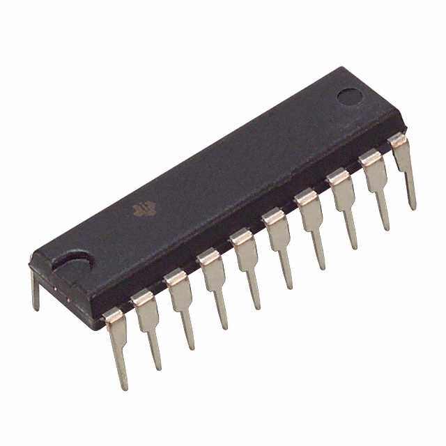
| 描述 | IC REG CTRLR BUCK BST 20DIP开关控制器 Phase Shift Resonant Controller |
| 产品分类 | |
| 品牌 | Texas Instruments |
| 产品手册 | |
| 产品图片 |
|
| rohs | 符合RoHS无铅 / 符合限制有害物质指令(RoHS)规范要求 |
| 产品系列 | 电源管理 IC,开关控制器 ,Texas Instruments UC3879N- |
| 数据手册 | |
| 产品型号 | UC3879N |
| PWM类型 | 电流/电压模式 |
| 产品目录页面 | |
| 产品种类 | 开关控制器 |
| 倍增器 | 无 |
| 其它名称 | 296-11335-5 |
| 分频器 | 无 |
| 包装 | 管件 |
| 升压 | 是 |
| 占空比 | 100% |
| 反向 | 无 |
| 反激式 | 无 |
| 商标 | Texas Instruments |
| 安装风格 | Through Hole |
| 封装 | Tube |
| 封装/外壳 | 20-DIP(0.300",7.62mm) |
| 封装/箱体 | PDIP-20 |
| 工作温度 | 0°C ~ 70°C |
| 工厂包装数量 | 20 |
| 开关频率 | 300 kHz |
| 最大工作温度 | + 70 C |
| 最小工作温度 | 0 C |
| 标准包装 | 20 |
| 电压-电源 | 11 V ~ 18 V |
| 类型 | Phase Shift Resonant Controller |
| 系列 | UC3879 |
| 输出数 | 4 |
| 输出电流 | 100 mA |
| 输出端数量 | 4 Output |
| 降压 | 是 |
| 隔离式 | 无 |
| 频率-最大值 | 300kHz |


- 商务部:美国ITC正式对集成电路等产品启动337调查
- 曝三星4nm工艺存在良率问题 高通将骁龙8 Gen1或转产台积电
- 太阳诱电将投资9.5亿元在常州建新厂生产MLCC 预计2023年完工
- 英特尔发布欧洲新工厂建设计划 深化IDM 2.0 战略
- 台积电先进制程称霸业界 有大客户加持明年业绩稳了
- 达到5530亿美元!SIA预计今年全球半导体销售额将创下新高
- 英特尔拟将自动驾驶子公司Mobileye上市 估值或超500亿美元
- 三星加码芯片和SET,合并消费电子和移动部门,撤换高东真等 CEO
- 三星电子宣布重大人事变动 还合并消费电子和移动部门
- 海关总署:前11个月进口集成电路产品价值2.52万亿元 增长14.8%


PDF Datasheet 数据手册内容提取
UC1879 UC2879 UC3879 www.ti.com SLUS230B–JUNE1998–REVISEDJUNE2007 PHASE SHIFT RESONANT CONTROLLER FEATURES DESCRIPTION • ProgrammableOutputTurnOnDelay;Zero The UC3879 controls a bridge power stage by phase DelayAvailable shifting the switching of one half-bridge with respect • CompatiblewithVoltageModeorCurrent to the other. This allows constant frequency pulse ModeTopologies width modulation in combination with resonant, zero-voltage switching for high efficiency • PracticalOperationatSwitchingFrequencies performance. The UC3879 can be configured to to300kHz provide control in either voltage mode or current • 10-MHzErrorAmplifier mode operation, with overcurrent shutdown for fast • PinProgrammableUndervoltageLockout faultprotection. • LowStartupCurrent–150m A Independently programmable time delays provide • SoftStartControl dead-time at the turn-on of each output stage, allowingtimeforeachresonantswitchinginterval. • OutputsActiveLowDuringUVLO BLOCK DIAGRAM Pleasebeawarethatanimportantnoticeconcerningavailability,standardwarranty,anduseincriticalapplicationsofTexas Instrumentssemiconductorproductsanddisclaimerstheretoappearsattheendofthisdatasheet. PRODUCTIONDATAinformationiscurrentasofpublicationdate. Copyright©1998–2007,TexasInstrumentsIncorporated Products conform to specifications per the terms of the Texas Instruments standard warranty. Production processing does not necessarilyincludetestingofallparameters.
UC1879 UC2879 UC3879 www.ti.com SLUS230B–JUNE1998–REVISEDJUNE2007 DESCRIPTION (CONTINUED) With the oscillator capable of operating in excess of 600 kHz, overall output switching frequencies to 300 kHz are practical. In addition to the standard free running mode, with the CLKSYNC pin, the user may configure the UC3879 to accept an external clock synchronization signal. Alternatively, up to three units can be locked togetherwiththeoperationalfrequencydeterminedbythefastestdevice. Protective features include an undervoltage lockout and overcurrent protection. Additional features include a 10-MHz error amplifier, a 5-V precision reference, and soft start. The UC3879 is available in 20 pin N, J, DW, andQand28pinLpackages. ABSOLUTE MAXIMUM RATINGS(1) PARAMETER VALUE UNIT Supplyvoltage(VC,VIN) 20 V Outputcurrent,sourceorsink,dc 20 Outputcurrent,source,sinkpeakfor0.1m satmaxfrequencyof300 mA 100 kHz Analoginputs (Pins1,2,3,4,5,6,14,15,17,18,19) –0.3to5.3 V (Pin16) –0.03toVIN Analogoutputs (Pins7,8,12,13) –0.3toV to0.3 V C Storagetemperaturerange –65(cid:176) Cto150(cid:176) C Junctiontemperature –55(cid:176) Cto150(cid:176) C (cid:176) C Leadtemperature(soldering,10sec) 300°C (1) Pinreferencesareto20-pinDILandSOICpackages.Allvoltagesarewithrespecttogroundunlessotherwisestated.Currentsare positiveinto,negativeoutofthespecifiedterminal. THERMAL CHARACTERISTICS overoperatingfree-airtemperaturerange(unlessotherwisenoted) PACKAGE q q JA JC J-20 70-85 28(1) N-20 80(2) 35 DW-20SOIC 45-95(2) 25 PLCC-20 43-75(2) 34 CLCC-20 N/A 5-8(2)(3) (1) q datavaluesstatedwerederivedfromMIL-STD-1835B.MIL-STD-1835Bstates"Thebaselinevaluesshownareworstcase(mean JC +2s)fora60x60milmicrocircuitdevicesilicondieandaplicablefordeviceswithdiesizesupto14400squaremils.Fordevicesdie sizesgreaterthan14400squaremilsusethefollowingvalues;dual-in-line,11(cid:176) C/W;flatpacl10(cid:176) C/W;pingridarray,10(cid:176) C/W". (2) Specifiedq (junction-to-ambient)isfordevicesmountedto5-in2FR4PCboardwithoneouncecopperwirewherenoted.When JA resistancerangeisgiven,lowervaluesarefor5-in2aluminumPCboard.TestPWBwas0.062inthickandtypicallyused0.635-mm tracewidthsforpowerpackagesand1.3-mmtracewidthsfornon-powerpackageswitha100x100milprobelandareaattheendof eachtrace. (3) q estimatedforbacksideofdevice,throughthemetalizedthermalconductionpads. JC 2 SubmitDocumentationFeedback
UC1879 UC2879 UC3879 www.ti.com SLUS230B–JUNE1998–REVISEDJUNE2007 ProductSelectionGuide TEMPERATURERANGE AVAILABLEPACKAGES UCC1879 –55(cid:176) Cto125(cid:176) C J,L UCC2879 –40(cid:176) Cto85(cid:176) C N,DW,Q,J,L UCC3879 0(cid:176) Cto70(cid:176) C N,DW,Q DIL-20, SOIC-2 J OR N PACKAGE, DW PACKAGE CLCC-28 (TOPVIEW) LPACKAGE (TOPVIEW) VREF 1 20 GND DELSETA-B CT UVSEL COMP 2 19 RAMP N/C CLKSYNC N/C N/C EA– 3 18 RT CS 4 17 CLKSYNC OUTC 4 6 7 8 9 10 11 RT DELSETC-D 5 16 UVSEL OUTB 3 13 RAMP SS 6 15 DELSETA-B PWRGND 2 14 GND VIN 1 15 N/C OUTD 7 14 CT VC 28 16 N/C OUTC 8 13 OUTA OUTC 27 17 VREF VC 9 12 OUTB OUTD 25 24 23 22 21 20 18 COMP VIN 10 11 PWRGND N/C EA– PLCC-20 N/C CS Q PACKAGE SS N/C (TOPVIEW) DELSETC-D DELSETC-D SS CS OUTD EA– 3 2 1 20 19 OUTC 4 18 COMP VC 5 17 VREF VIN 6 16 GND PWRGND 7 15 RAMP OUTB 8 14 RT 9 10 11 12 13 OUTA CLKSYNC CT UVSEL DELSETA-B SubmitDocumentationFeedback 3
UC1879 UC2879 UC3879 www.ti.com SLUS230B–JUNE1998–REVISEDJUNE2007 ELECTRICAL CHARACTERISTICS Unlessspecified;VC=VIN=V =12V,CT=470pF,RT=9.53k,R =R =4.8k,C =C UVSEL DELSETA-B DELSEC-D DELSETA-B DELSETC-D =0.01m F,T =T. A J PARAMETER TESTCONDITIONS MIN TYP MAX UNIT UndervoltageLockout V =VIN 9 10.75 12.5 UVSEL Startthreshold V =Open 12.5 15.25 16.5 UVSEL V V =VIN 1.15 1.75 2.15 UVSEL UVLOhysteresis V =Open 5.2 6 7.4 UVSEL Inputbias,UVSELpin V =VIN=8V 30 m A UVSEL SupplyCurrent VIN=V =8V,VC=18V, I startup UVSEL 150 600 VIN I =I DELSETA-B DELSETC-D=0 m A VIN=V =8V,VC=18V, I startup UVSEL 10 100 VC I =I DELSETA-B DELSETC-D=0 UC3879,UC2879 23 35 I operating VIN UC1879 23 36 mA I operating 4 8 VC VoltageReference Outputvoltage T =25(cid:176) C 4.92 5 5.08 V J Lineregulation 11V<VIN<18V 1 10 mV Loadregulation I =–10mA 5 20 VREF Totalvariation Line,Load,Temperature 4.875 5.125 V Shortcircuitcurrent VREF=0V,T =25(cid:176) C –60 –15 mA J ErrorAmplifier Erroramplifierinputvoltage 2.4 2.5 2.6 V Inputbiascurrent 0.6 3 m A AVOL 1V<VCOMP<4V 60 90 dB PSRR 11V<VIN<18V 85 100 Outputsinkcurrent V =1V 1 2.5 COMP mA Outputsourcecurrent V =4V –1.3 –0.5 COMP Outputvoltagehigh I =–0.5mA 4 4.7 5 COMP V Outputvoltagelow I =1mA 0 0.5 1 COMP Slewrate T =25(cid:176) C 6 11 V/m s A 4 SubmitDocumentationFeedback
UC1879 UC2879 UC3879 www.ti.com SLUS230B–JUNE1998–REVISEDJUNE2007 ELECTRICAL CHARACTERISTICS (continued) Unlessspecified;VC=VIN=V =12V,CT=470pF,RT=9.53k,R =R =4.8k,C =C UVSEL DELSETA-B DELSEC-D DELSETA-B DELSETC-D =0.01m F,T =T. A J PARAMETER TESTCONDITIONS MIN TYP MAX UNIT PWMComparator RAMPoffsetvoltage T =25(cid:176) C(1) 1.1 1.25 1.4 V J PWMphaseshift, VCOMP>VRAMPpeak+VRAMPoffset 98% 99.7% 102% TDELSETA-B,TDELSETC-D=0(2) VCOMP<ZeroPhaseShiftVoltage 0% 0.3% 2% Outputskew, VCOMP>VRAMPpeak+VRAMPoffset 10 TDELSETA-B,TDELSETC-D=0(2) VCOMP<ZeroPhaseShiftVoltage 10 ns Ramptooutputdelay, UC3879,UC2879 115 250 TDELSETA-B=0,TDELSETC-D=0 UC1879 115 300 Oscillator Initialaccuracy T =25(cid:176) C 180 200 220 kHz A Voltagestability 11V<VIN<18V 1 2 % Totalvariation Line,Temperature 160 200 240 kHz CLKSYNCthreshold 2.3 2.5 2.7 Clockouthigh 2.8 4 V Clockoutlow 0.5 1 1.5 Clockoutpulsewidth 400 600 ns Rampvalleyvoltage 0.2 0.4 V Ramppeakvoltage 2.8 2.9 3.2 CurrentLimit Inputbias V =3V 2 10 m A CS Thresholdvoltage 2.35 2.5 2.65 V DelaytoOUTA,B,C,D 160 300 ns Cycle-by-CycleCurrentLimit Inputbias V =2.2V 2 10 m A CS Thresholdvoltage 1.85 2 2.15 V Delaytooutputzerophase 110 300 ns (1) Rampoffsetvoltagehasatemperaturecoefficientofabout–4mV/(cid:176) C. 200 q= f% T (2) Phaseshiftpercentage(0%=0,100%=180)isdefinedas whereisthephaseshift,andandTaredefinedinFigure1.At0%phaseshift,istheoutputskew. SubmitDocumentationFeedback 5
UC1879 UC2879 UC3879 www.ti.com SLUS230B–JUNE1998–REVISEDJUNE2007 ELECTRICAL CHARACTERISTICS (continued) Unlessspecified;VC=VIN=V =12V,CT=470pF,RT=9.53k,R =R =4.8k,C =C UVSEL DELSETA-B DELSEC-D DELSETA-B DELSETC-D =0.01m F,T =T. A J PARAMETER TESTCONDITIONS MIN TYP MAX UNIT SoftStart/ResetDelay Chargecurrent V =0.5V –20 –9 –3 SS m A Dischargecurrent V =1V 120 230 SS Restartthreshold 4.3 4.7 V Dischargelevel 300 mV OutputDrivers OutputLowlevel I =10mA 0.3 0.4 OUT V OutputHighlevel I =–10mA,ReferencedtoVC 2.2 3 OUT DelaySet (3) Delaytime(4) R =R =4.8k 250 370 520 DELSETA-B DELSETC-D Delaytime(4) R =R =1.9k 100 155 220 ns DELSETA-B DELSETC-D Zerodelay(5) V =V =5V 5 DELSETA-B DELSETC-D (3) Delaytimecanbeprogrammedviaresistorsfromthedelaysetpinstoground. DelayTime=(0.89·10-10·RDELAY)sec TherecommendedrangeforR is1.9kW to10kW . DELAY (4) Delaytimeisdefinedas: æ1 ö delay=T·ç2-dutycycle÷ è ø whereTisdefinedinFigure1. (5) ThezerophaseshiftvoltageisthevoltagemeasuredatCOMPwhichforceszerophaseshift.Thisconditioncorrespondstozero effectiveoutputpower.Zerophaseshiftvoltagehasatemperaturecoefficientofabout–2mV/(cid:176) C. t DutyCycle= T Period=T TDHL(AtoC)=TDHL(BtoD)= Figure1.PhaseShift,OutputSkewandDelayTimeDefinitions 6 SubmitDocumentationFeedback
UC1879 UC2879 UC3879 www.ti.com SLUS230B–JUNE1998–REVISEDJUNE2007 PIN DESCRIPTIONS CLKSYNC (Bi-directional Clock and Synchronization): Used as an output, CLKSYNC provides a clock signal. As an input, this pin provides a synchronization point. Multiple UC3879s, each with their own local oscillator frequency, may be connected together by the CLKSYNC pin, and they will synchronize to the fastest oscillator. This pin may also be used to synchronize the UC3879 to an external clock, provided the frequency of the externalsignalishigherthanthefrequencyofthelocaloscillator. CLKSYNC is internally connected to an emitter follower pull-up and a current source pull-down (300 m A typical). Therefore, an external resistor to GND can be usedtoimprovetheCLKSYNCpin’sabilitytodrivecapacitiveloads. COMP (Error Amplifier Output): This pin is the output of the gain stage for overall feedback control. Error amplifier output voltage levels below 0.9 V forces zero phase shift. Since the error amplifier has a relatively low currentdrivecapability,theoutputmaybeoverriddenbydrivingitwithasufficientlylowimpedancesource. CT (Oscillator Frequency Set): After choosing RT to set the required upper end of the linear duty cycle range, thetimingcapacitor(CT)valueiscalculatedtosettheoscillatorfrequencyasfollows: Dlin CT= 1.08·RT·f Connect the timing capacitor directly between CT and GND. Use a high quality ceramic capacitor with low ESL and ESR for best results. A minimum CT value of 200 pF insures good accuracy and less susceptibility to circuit layoutparasitics.TheoscillatorandPWMaredesignedtoprovidepracticaloperationto600kHz. CS (Current Sense): This pin is the non-inverting input to the two current fault comparators whose references are set internally to fixed values of 2 V and 2.5 V. When the voltage at this pin exceeds 2 V, and the error amplifier output voltage exceeds the voltage on the ramp input, the phase shift limiting overcurrent comparator will limit the phase shifting on a cycle-by-cycle basis. When the voltage at this pin exceeds 2.5 V, the current fault latch is set, the outputs are forced OFF, and a soft start cycle is initiated. If a constant voltage above 2.5 V is applied to this pin the outputs are disabled and held low. When CS is brought below 2.5 V, the outputs will begin switching at 0 degrees phase shift before the SS pin begins to rise. This condition will not prematurely deliverpowertotheload. DELSETA-B, DELSETC-D (Output Delay Control): The user programmed currents from these pins to GND set the turn on delay for the corresponding output pair. This delay is introduced between the turn off of one switch and the turn on of another in the same leg of the bridge to allow resonant switching to take place. Separate delays are provided for the two half-bridges to accommodate differences in the resonant capacitor charging currents. EA– (Error Amplifier Inverting Input): This is normally connected to the voltage divider resistors which sense the power supply output voltage level. The loop compensation components are connected between this pin and COMP. GND (Signal Ground): All voltages are measured with respect to GND. The timing capacitor on CT, and bypass capacitorsonVREFandVINshouldbeconnecteddirectlytothegroundplanenearGND. OUTA – OUTD (Outputs A-D): The outputs are 100-mA totem pole output drivers optimized to drive FET driver devices. The outputs operate as pairs with a nominal 50% duty cycle. The A-B pair is intended to drive one half-bridge in the external power stage and is synchronized to the clock waveform. The C-D pair drives the other half-bridgewithswitchingphaseshiftedwithrespecttotheA-Boutputs. PWRGND (Power Ground): VC should be bypassed with a ceramic capacitor from VC to the section of the ground plane that is connected to PWRGND. Any required bulk reservoir capacitor should be connected in parallel. PWRGND and GND should be connected at a single point near the chip to optimize noise rejection and minimizeDCvoltagedrops. RAMP (Voltage Ramp): This pin is the input to the PWM comparator. Connect it to CT for voltage mode control. For current mode control, connect RAMP to CS and also to the output of the current sense transformer circuit. SlopecompensationcanbeachievedbyinjectingaportionoftherampvoltagefromCTtoRAMP. SubmitDocumentationFeedback 7
UC1879 UC2879 UC3879 www.ti.com SLUS230B–JUNE1998–REVISEDJUNE2007 PIN DESCRIPTIONS (continued) RT (Clock/Sync Duty Cycle Set Pin): The UC3879 oscillator produces a sawtooth waveform. The rising edge is generated by connecting a resistor from RT to GND and a capacitor from CT to GND (see CT pin description). During the rising edge, the modulator has linear control of the duty cycle. The duty cycle jumps to 100% when the voltage on COMP exceeds the oscillator peak voltage. Selection of RT should be done first, based on the requiredupperendofthelineardutycyclerange(D )asfollows: lin 2.5 RT= 10mA·(1-Dlin) RecommendedvaluesforRTrangefrom2.5kW to100kW . SS: Connect a capacitor between this pin and GND to set the soft start time. The voltage at SS will remain near zero volts as long as VIN is below the UVLO threshold. Soft start will be pulled up to about 4.8 V by an internal 9-m A current source when VIN and VREF become valid (assuming a non-fault condition). In the event of a current fault (CS voltage exceeding 2.5 V), soft start will be pulled to GND and then ramp to 4.8 V. If a fault occurs during the soft start cycle, the outputs will be immediately disabled and soft start must fully charge prior to resetting the fault latch. For paralleled controllers, the soft start pins may be paralleled to a single capacitor, butthechargecurrentswillbeadditive. UVSEL:Connecting this pin to VIN sets a turn on voltage of 10.75 V with 1.5 V of UVLO hysteresis. Leaving the pinopen-circuitedprogramsaturnonvoltageof15.25Vwith6Vofhysteresis. VC (Output Switch Supply Voltage): This pin supplies power to the output drivers and their associated bias circuitry.Thedifferencebetweentheoutputhighdrive and VC is typically 2.1 V. This supply should be bypassed directlytoPWRGNDwithalowESR/ESLcapacitor. VIN (Primary Chip Supply Voltage): This pin supplies power to the logic and analog circuitry on the integrated circuit that is not directly associated with driving the output stages. Connect VIN to a stable source above 12 V for normal operation. To ensure proper functionality, the UC3879 is inactive until VIN exceeds the upper undervoltagelockoutthreshold.ThispinshouldbebypasseddirectlytoGNDwithalowESR/ESLcapacitor. NOTE: When VIN exceeds the UVLO threshold the supply current (I ) jumps from about 100 IN Atogreaterthan20 mA. If the UC3879 is not connected to a well bypassed supply, it may immediately enter the UVLO state again. Therefore, sufficient bypass capacity mustbeaddedtoensurereliablestartup. VREF: This pin provides an accurate 5 V voltage reference. It is internally short circuit current limited. VREF is disabled while VIN is below the UVLO threshold. The circuit is also disabled until VREF reaches approximately 4.75V.ForbestresultsbypassVREFwitha0.1m F,lowESR/ESLcapacitor. ADDITIONAL INFORMATION Please refer to the following Unitrode publications for additional information. The following three topics are availableintheApplicationsHandbook. 1. Application Note U-154, The New UC3879 Phase- Shifted PWM Controller Simplifies the Design of Zero VoltageTransitionFull-BridgeConverters,byLaszloBalogh. 2. Application Note U-136, Phase Shifted, Zero Voltage Transition Design Considerations and the UC3875 PWMController,byBillAndreycak. 3. Design Note DN-63, The Current-Doubler Rectifier: An Alternative Rectification Technique for Push-Pull andBridgeConverters,byLaszloBalogh. 8 SubmitDocumentationFeedback
PACKAGE OPTION ADDENDUM www.ti.com 6-Feb-2020 PACKAGING INFORMATION Orderable Device Status Package Type Package Pins Package Eco Plan Lead/Ball Finish MSL Peak Temp Op Temp (°C) Device Marking Samples (1) Drawing Qty (2) (6) (3) (4/5) UC2879DW ACTIVE SOIC DW 20 25 Green (RoHS NIPDAU Level-2-260C-1 YEAR -40 to 85 UC2879DW & no Sb/Br) UC2879DWG4 ACTIVE SOIC DW 20 25 Green (RoHS NIPDAU Level-2-260C-1 YEAR -40 to 85 UC2879DW & no Sb/Br) UC2879DWTR ACTIVE SOIC DW 20 2000 Green (RoHS NIPDAU Level-2-260C-1 YEAR -40 to 85 UC2879DW & no Sb/Br) UC2879DWTRG4 ACTIVE SOIC DW 20 2000 Green (RoHS NIPDAU Level-2-260C-1 YEAR -40 to 85 UC2879DW & no Sb/Br) UC2879N ACTIVE PDIP N 20 18 Green (RoHS NIPDAU N / A for Pkg Type -40 to 85 UC2879N & no Sb/Br) UC2879NG4 ACTIVE PDIP N 20 18 Green (RoHS NIPDAU N / A for Pkg Type -40 to 85 UC2879N & no Sb/Br) UC3879DW ACTIVE SOIC DW 20 25 Green (RoHS NIPDAU Level-2-260C-1 YEAR 0 to 70 UC3879DW & no Sb/Br) UC3879DWG4 ACTIVE SOIC DW 20 25 Green (RoHS NIPDAU Level-2-260C-1 YEAR 0 to 70 UC3879DW & no Sb/Br) UC3879DWTR ACTIVE SOIC DW 20 2000 Green (RoHS NIPDAU Level-2-260C-1 YEAR 0 to 70 UC3879DW & no Sb/Br) UC3879N ACTIVE PDIP N 20 18 Green (RoHS NIPDAU N / A for Pkg Type 0 to 70 UC3879N & no Sb/Br) (1) The marketing status values are defined as follows: ACTIVE: Product device recommended for new designs. LIFEBUY: TI has announced that the device will be discontinued, and a lifetime-buy period is in effect. NRND: Not recommended for new designs. Device is in production to support existing customers, but TI does not recommend using this part in a new design. PREVIEW: Device has been announced but is not in production. Samples may or may not be available. OBSOLETE: TI has discontinued the production of the device. (2) RoHS: TI defines "RoHS" to mean semiconductor products that are compliant with the current EU RoHS requirements for all 10 RoHS substances, including the requirement that RoHS substance do not exceed 0.1% by weight in homogeneous materials. Where designed to be soldered at high temperatures, "RoHS" products are suitable for use in specified lead-free processes. TI may reference these types of products as "Pb-Free". RoHS Exempt: TI defines "RoHS Exempt" to mean products that contain lead but are compliant with EU RoHS pursuant to a specific EU RoHS exemption. Green: TI defines "Green" to mean the content of Chlorine (Cl) and Bromine (Br) based flame retardants meet JS709B low halogen requirements of <=1000ppm threshold. Antimony trioxide based flame retardants must also meet the <=1000ppm threshold requirement. (3) MSL, Peak Temp. - The Moisture Sensitivity Level rating according to the JEDEC industry standard classifications, and peak solder temperature. Addendum-Page 1
PACKAGE OPTION ADDENDUM www.ti.com 6-Feb-2020 (4) There may be additional marking, which relates to the logo, the lot trace code information, or the environmental category on the device. (5) Multiple Device Markings will be inside parentheses. Only one Device Marking contained in parentheses and separated by a "~" will appear on a device. If a line is indented then it is a continuation of the previous line and the two combined represent the entire Device Marking for that device. (6) Lead/Ball Finish - Orderable Devices may have multiple material finish options. Finish options are separated by a vertical ruled line. Lead/Ball Finish values may wrap to two lines if the finish value exceeds the maximum column width. Important Information and Disclaimer:The information provided on this page represents TI's knowledge and belief as of the date that it is provided. TI bases its knowledge and belief on information provided by third parties, and makes no representation or warranty as to the accuracy of such information. Efforts are underway to better integrate information from third parties. TI has taken and continues to take reasonable steps to provide representative and accurate information but may not have conducted destructive testing or chemical analysis on incoming materials and chemicals. TI and TI suppliers consider certain information to be proprietary, and thus CAS numbers and other limited information may not be available for release. In no event shall TI's liability arising out of such information exceed the total purchase price of the TI part(s) at issue in this document sold by TI to Customer on an annual basis. Addendum-Page 2
PACKAGE MATERIALS INFORMATION www.ti.com 11-Oct-2013 TAPE AND REEL INFORMATION *Alldimensionsarenominal Device Package Package Pins SPQ Reel Reel A0 B0 K0 P1 W Pin1 Type Drawing Diameter Width (mm) (mm) (mm) (mm) (mm) Quadrant (mm) W1(mm) UC2879DWTR SOIC DW 20 2000 330.0 24.4 10.8 13.3 2.7 12.0 24.0 Q1 UC3879DWTR SOIC DW 20 2000 330.0 24.4 10.8 13.3 2.7 12.0 24.0 Q1 PackMaterials-Page1
PACKAGE MATERIALS INFORMATION www.ti.com 11-Oct-2013 *Alldimensionsarenominal Device PackageType PackageDrawing Pins SPQ Length(mm) Width(mm) Height(mm) UC2879DWTR SOIC DW 20 2000 367.0 367.0 45.0 UC3879DWTR SOIC DW 20 2000 367.0 367.0 45.0 PackMaterials-Page2
None
PACKAGE OUTLINE DW0020A SOIC - 2.65 mm max height SCALE 1.200 SOIC C 10.63 SEATING PLANE TYP 9.97 A PIN 1 ID 0.1 C AREA 18X 1.27 20 1 13.0 2X 12.6 11.43 NOTE 3 10 11 0.51 20X 7.6 0.31 2.65 MAX B 7.4 0.25 C A B NOTE 4 0.33 TYP 0.10 0.25 SEE DETAIL A GAGE PLANE 0.3 1.27 0 - 8 0.1 0.40 DETAIL A TYPICAL 4220724/A 05/2016 NOTES: 1. All linear dimensions are in millimeters. Dimensions in parenthesis are for reference only. Dimensioning and tolerancing per ASME Y14.5M. 2. This drawing is subject to change without notice. 3. This dimension does not include mold flash, protrusions, or gate burrs. Mold flash, protrusions, or gate burrs shall not exceed 0.15 mm per side. 4. This dimension does not include interlead flash. Interlead flash shall not exceed 0.43 mm per side. 5. Reference JEDEC registration MS-013. www.ti.com
EXAMPLE BOARD LAYOUT DW0020A SOIC - 2.65 mm max height SOIC 20X (2) SYMM 1 20 20X (0.6) 18X (1.27) SYMM (R0.05) TYP 10 11 (9.3) LAND PATTERN EXAMPLE SCALE:6X SOOPLEDNEINRG MASK METAL MSOELTDAEL RU NMDAESRK SOOPLEDNEINRG MASK 0.07 MAX 0.07 MIN ALL AROUND ALL AROUND NON SOLDER MASK SOLDER MASK DEFINED DEFINED SOLDER MASK DETAILS 4220724/A 05/2016 NOTES: (continued) 6. Publication IPC-7351 may have alternate designs. 7. Solder mask tolerances between and around signal pads can vary based on board fabrication site. www.ti.com
EXAMPLE STENCIL DESIGN DW0020A SOIC - 2.65 mm max height SOIC 20X (2) SYMM 1 20 20X (0.6) 18X (1.27) SYMM 10 11 (9.3) SOLDER PASTE EXAMPLE BASED ON 0.125 mm THICK STENCIL SCALE:6X 4220724/A 05/2016 NOTES: (continued) 8. Laser cutting apertures with trapezoidal walls and rounded corners may offer better paste release. IPC-7525 may have alternate design recommendations. 9. Board assembly site may have different recommendations for stencil design. www.ti.com
IMPORTANTNOTICEANDDISCLAIMER TI PROVIDES TECHNICAL AND RELIABILITY DATA (INCLUDING DATASHEETS), DESIGN RESOURCES (INCLUDING REFERENCE DESIGNS), APPLICATION OR OTHER DESIGN ADVICE, WEB TOOLS, SAFETY INFORMATION, AND OTHER RESOURCES “AS IS” AND WITH ALL FAULTS, AND DISCLAIMS ALL WARRANTIES, EXPRESS AND IMPLIED, INCLUDING WITHOUT LIMITATION ANY IMPLIED WARRANTIES OF MERCHANTABILITY, FITNESS FOR A PARTICULAR PURPOSE OR NON-INFRINGEMENT OF THIRD PARTY INTELLECTUAL PROPERTY RIGHTS. These resources are intended for skilled developers designing with TI products. You are solely responsible for (1) selecting the appropriate TI products for your application, (2) designing, validating and testing your application, and (3) ensuring your application meets applicable standards, and any other safety, security, or other requirements. These resources are subject to change without notice. TI grants you permission to use these resources only for development of an application that uses the TI products described in the resource. Other reproduction and display of these resources is prohibited. No license is granted to any other TI intellectual property right or to any third party intellectual property right. TI disclaims responsibility for, and you will fully indemnify TI and its representatives against, any claims, damages, costs, losses, and liabilities arising out of your use of these resources. TI’s products are provided subject to TI’s Terms of Sale (www.ti.com/legal/termsofsale.html) or other applicable terms available either on ti.com or provided in conjunction with such TI products. TI’s provision of these resources does not expand or otherwise alter TI’s applicable warranties or warranty disclaimers for TI products. Mailing Address: Texas Instruments, Post Office Box 655303, Dallas, Texas 75265 Copyright © 2020, Texas Instruments Incorporated