ICGOO在线商城 > UC3872N
 Datasheet下载
- 型号: UC3872N
- 制造商: Texas Instruments
- 库位|库存: xxxx|xxxx
- 要求:
| 数量阶梯 | 香港交货 | 国内含税 |
| +xxxx | $xxxx | ¥xxxx |
查看当月历史价格
查看今年历史价格
UC3872N产品简介:
ICGOO电子元器件商城为您提供UC3872N由Texas Instruments设计生产,在icgoo商城现货销售,并且可以通过原厂、代理商等渠道进行代购。 提供UC3872N价格参考¥询价-¥询价以及Texas InstrumentsUC3872N封装/规格参数等产品信息。 你可以下载UC3872N参考资料、Datasheet数据手册功能说明书, 资料中有UC3872N详细功能的应用电路图电压和使用方法及教程。
| 参数 | 数值 |
| 产品目录 | 集成电路 (IC)半导体 |
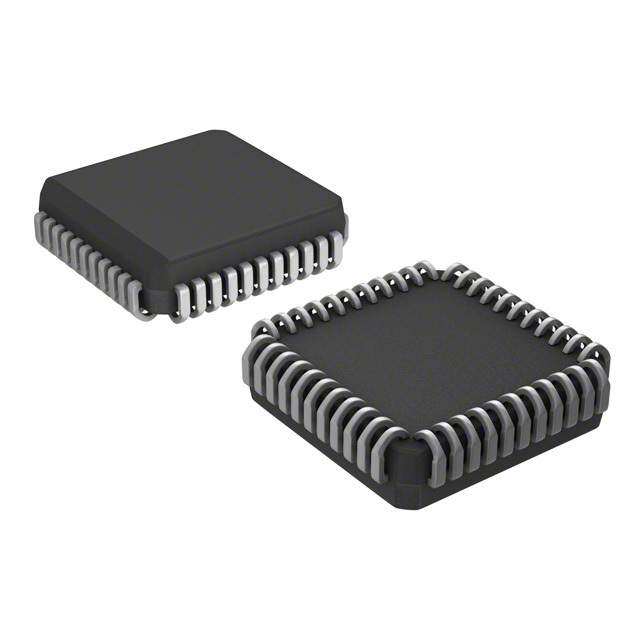
| 描述 | IC LAMP BALLAST CNTRLR 14-DIP显示驱动器和控制器 Resonant Lamp Ballast Controller |
| 产品分类 | |
| 品牌 | Texas Instruments |
| 产品手册 | |
| 产品图片 |
|
| rohs | 符合RoHS无铅 / 符合限制有害物质指令(RoHS)规范要求 |
| 产品系列 | 驱动器IC,显示驱动器和控制器,Texas Instruments UC3872N- |
| 数据手册 | http://www.ti.com/lit/pdf/slus178 |
| 产品型号 | UC3872N |
| 产品 | Fluorescent Lamp Driver |
| 产品目录页面 | |
| 产品种类 | 显示驱动器和控制器 |
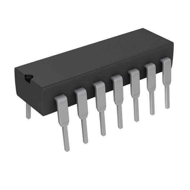
| 供应商器件封装 | 14-PDIP |
| 其它名称 | 296-11330-5 |
| 制造商卷带宽度 | - |
| 制造商卷带材料 | - |
| 制造商卷带直径 | - |
| 包装 | 管件 |
| 商标 | Texas Instruments |
| 图号 | 296; 4040049; N; 14 |
| 安装类型 | 通孔 |
| 安装风格 | Through Hole |
| 封装 | Tube |
| 封装/外壳 | 14-DIP(0.300",7.62mm) |
| 封装/箱体 | PDIP-14 |
| 工作温度 | 0°C ~ 70°C |
| 工厂包装数量 | 25 |
| 最大功率耗散 | 1 W |
| 最大工作温度 | + 70 C |
| 最小工作温度 | 0 C |
| 标准包装 | 25 |
| 电压-电源 | 4.5 V ~ 24 V |
| 电流-灌/拉输出 | - |
| 电流-电源 | 6mA |
| 电源电压 | 4.5 V to 24 V |
| 电源电流 | 6 mA |
| 类型 | 镇流器控制器 |
| 系列 | UC3872 |
| 调光 | 无 |
| 频率 | 57kHz ~ 78kHz |


- 商务部:美国ITC正式对集成电路等产品启动337调查
- 曝三星4nm工艺存在良率问题 高通将骁龙8 Gen1或转产台积电
- 太阳诱电将投资9.5亿元在常州建新厂生产MLCC 预计2023年完工
- 英特尔发布欧洲新工厂建设计划 深化IDM 2.0 战略
- 台积电先进制程称霸业界 有大客户加持明年业绩稳了
- 达到5530亿美元!SIA预计今年全球半导体销售额将创下新高
- 英特尔拟将自动驾驶子公司Mobileye上市 估值或超500亿美元
- 三星加码芯片和SET,合并消费电子和移动部门,撤换高东真等 CEO
- 三星电子宣布重大人事变动 还合并消费电子和移动部门
- 海关总署:前11个月进口集成电路产品价值2.52万亿元 增长14.8%

PDF Datasheet 数据手册内容提取
application UC1872 INFO UC2872 available UC3872 Resonant Lamp Ballast Controller FEATURES DESCRIPTION • Controls Different Types of Lamps: The UC3872 is a resonant lamp ballast controller optimized for driving Cold Cathode Fluorescent, Neon, and cold cathode fluorescent, neon, and other gas discharge lamps.The res- Gas Discharge onant power stage develops a sinusoidal lamp drive voltage, and mini- • Zero Voltage Switching (ZVS) of mizes switching loss and EMI generation. Lamp intensity adjustment is accomplishedwithabuckregulator,whichissynchronizedtotheexternal Push-Pull Drivers power stage’s resonant frequency. Suitable for automotive and battery • Accurate Control of Lamp Current powered applications, the UC3872 draws only 1µA when disabled. • Variable Lamp Intensity Control Soft start and open lamp detect circuitry have been incorporated to mini- • 1µA Disable Current mizecomponentstresses.Openlampdetectionisenabledatthecomple- tion of a soft start cycle. The chip is optimized for smooth duty cycle • 4.5V to 24V Operation control to 100%. • Open Lamp Detection Circuitry Other features include a precision 1.2% reference, undervoltage lockout, and accurate minimum and maximum frequency control. BLOCK DIAGRAM 3 VC 3.0V 2 AOUT VCC 10 UVLO REF 50k REF 9 (HIGH=ENABLE) PUSHPULL ENBL 11 OUTPUTS 0.1V + N-CHANNEL – COMP 4 INV 6 – OPEN TOGGLE 1 BOUT 20µA +EA LAMP DETECT T 50k 1.5V – PWM SS 5 – 1 + 200µA 0.2V R CT 7 + S 50k OSCILLATOR SENSE 12 COUT ZERODETECT OUT ZD 8 – BUCKDRIVE 0.5V + SYNC P-CHANNEL 13 PGND 14 GND Note:Pin numbers shown are for DIP package. UDG-99112 07/99
UC1872 UC2872 UC3872 ABSOLUTE MAXIMUM RATINGS CONNECTION DIAGRAMS Analog Inputs. . . . . . . . . . . . . . . . . . . . . . . . . . . . .−0.3 to +10V SOIC-16,SSOP-16 (TOP VIEW) VCC, VC Voltage. . . . . . . . . . . . . . . . . . . . . . . . . . . . . . . .+24V DW,M Package ZD Input Current High Impedance Source . . . . . . . . . . . . . . . . . . . . . .+10mA ZD Input Voltage Low Impedance Source . . . . . . . . . . . . . . . . . . . . . . . .+24V Power Dissipation at TA= 25°C. . . . . . . . . . . . . . . . . . . . . .1W Storage Temperature. . . . . . . . . . . . . . . . . . .−65°C to +150°C Lead Temperature. . . . . . . . . . . . . . . . . . . . . . . . . . . . . .300°C Note1:Currentsarepositiveinto,negativeoutofthespecified terminal. Note2:ConsultPackagingSectionofDatabookforthermallimi- tations and considerations of package. DIL-14 (TOP VIEW) PLCC-20 (Top View) N Package Q Package ELECTRICAL CHARACTERISTICS:Unless otherwise stated, these parameters apply for TJ=−55°C to +125°C for the UC1872, –40°C to +85°C for the UC2872,−0°C to +70°C for the UC3872; VCC= 5V, VC = 15V, VENBL= 5V, CT = 1nF, ZD = 1V. PARAMETER TEST CONDITIONS MIN TYP MAX UNITS Reference Section Output Voltage TJ= 25°C 2.963 3.000 3.037 V Over Temperature 2.940 3.000 3.060 V Line Regulation VCC = 4.75V to 18V 10 mV Load Regulation I = 0 to−5mA 10 mV O Oscillator Section Free Running Frequency T = 25°C 57 68 78 kHz J Maximum Synchronization Frequency T = 25°C 160 200 240 kHz J Charge Current V = 1.5V 180 200 220 µA CT Voltage Stability 2 % Temperature Stability 4 8 % Zero Detect Threshold 0.46 0.5 0.56 V Error Amp Section Input Voltage V = 2V 1.445 1.475 1.505 V O Input Bias Current −0.4 −2 µA Open Loop Gain V = 0.5 to 3V 65 90 dB O Output High V = 1.3V 3.1 3.5 3.9 V INV 2
UC1872 UC2872 UC3872 ELECTRICAL CHARACTERISTICS:Unless otherwise stated, these parameters apply for TJ=−55°C to +125°C for the UC1872, –40°C to +85°C for the UC2872,−0°C to +70°C for the UC3872; VCC= 5V, VC = 15V, VENBL= 5V, CT = 1nF, ZD = 1V. PARAMETER TEST CONDITIONS MIN TYP MAX UNITS Error Amp Section (cont.) Output Low V = 1.7V 0.1 0.2 V INV Output Source Current VINV= 1.3V, VO= 2V –350 –500 µA Output Sink Current V = 1.7V, V = 2V 10 20 mA INV O Common Mode Range 0 VIN-1V V Unity Gain Bandwidth T = 25°C (Note 4) 1 MHz J Open Lamp Detect Section Soft Start Threshold V = 0V 2.9 3.4 3.8 V INV Open Lamp Detect Threshold V = 4.2V 0.6 1.0 1.4 V SS Soft Start Current V = 2V 10 20 40 µA SS Output Section Output Low Level I = 0, Outputs A and B 0.05 0.2 V OUT I = 10mA 0.1 0.4 V OUT I = 100mA 1.5 2.2 V OUT Output High Level I = 0, Output C 13.9 14.9 V OUT I =−10mA 13.5 14.3 V OUT I =−100mA 12.5 13.5 V OUT Rise Time T = 25°C, Cl = 1nF (Note 4) 30 80 ns J Fall Time T = 25°C, Cl = 1nF (Note 4) 30 80 ns J Output Dynamics Out A and B Duty Cycle 48 49.9 50 % Out C Max Duty Cycle V = 1V 100 % INV Out C Min Duty Cycle V = 2V 0 % INV Under Voltage Lockout Section Startup Threshold Voltage 3.7 4.2 4.5 V Hysteresis 120 200 280 mV Enable Section Input High Threshold 2 V Input Low Threshold 0.8 V Input Current V = 5V 150 400 µA ENBL Supply Current Section VCC Supply Current VCC = 24V 6 14 mA VC Supply Current VC = 24V 5 12 mA ICC Disabled VCC = 24V, VENBL= 0V 1 10 µA Note3:Unlessotherwisespecified,allvoltagesarewithrespecttoground.Currentsarepositiveinto,andnegativeoutofthe specified terminal. Note 4:Guaranteed by design.Not 100% tested in production. 3
UC1872 UC2872 UC3872 PIN DESCRIPTIONS AOUT, BOUT: These outputs provide complementary INV: This pin is the inverting input to the error amplifier drive signals for the push-pull N-channel MOSFETs. and the input for the open lamp detect circuitry. If the Each one is high for 50% of the time, switching states voltage at INV is below the 1V open lamp detect thresh- each time a zero-detect is sensed. old, the outputs are disabled. COMP: COMP is the output terminal of the error ampli- PGND:Thispinisthehighcurrentgroundconnectionfor fier. Compensation components are normally connected the three output drivers. between COMP and INV. Connecting a capacitor from REF: This pin is connected to the 3V reference voltage this pin to ground limits turn on current and blanks the which is used for the internal logic. Bypass REF to open lamp detect signal allowing the lamp to start. groundwitha0.01µFceramiccapacitorforproperopera- COUT: This output directly drives the bulk regulator tion. P-channel MOSFET. COUT turn-on is synchronized to VC: VC is the power supply voltage connection for the eachzero-detect,andthereforeswitchesattwicethefre- output drivers.Bypass it to ground with a 0.1µF ceramic quency of AOUT and BOUT. The modulator controlling capacitor for proper operation. COUTisdesignedtoprovidesmoothcontrolupto100% duty cycle. VCC: VCC is the positive supply voltage for the chip.Its operating range is from 4.2V to 24V. Bypass VCC to CT: A capacitor connected between this pin and GND ground with a 0.1µF ceramic capacitor for proper opera- ground sets the synchronization frequency range. The tion. capacitor is charged with approximately 200µA, creating a linear ramp which is used by COUT’s (buck regulator ZD: The zero-detect input senses when the trans- driver) PWM comparator. former’s primary center tap voltage falls to zero to syn- chronize the sawtooth voltage waveform on CT. The ENBL:When ENBL is driven high the device is enabled. threshold is approximately 0.5V, providing a small When ENBL is pulled low, the IC is shut down and typi- amount of offset such that with propagation delay, cally draws 1µA. zero-volt switching occurs. A resistor (typically 10k) GND:This pin is the ground reference point for the inter- should be connected between ZD and the primary cen- nal reference and all thresholds. ter tap to limit input current at turn off. APPLICATION INFORMATION Figure 1 shows a complete application circuit using the form falls to zero. The actual threshold is 0.5 volts, UC3872 Resonant Lamp Ballast Controller. The IC pro- providing a small amount of anticipation to offset propa- vides all drive, control and housekeeping functions. The gation delay. buckoutputvoltage(transformercenter-tap)providesthe The synchronization pulse width is the time required for zero crossing and synchronization signals. the 4mA current sink to discharge the timing capacitor to The buck modulator drives a P-channel MOSFET di- 0.1 volts.This pulse width limits the minimum linear con- rectly, and operates over a 0-100% duty-cycle range. trol range of the buck regulator. The 200µA current Themodulationrangeincludes100%,allowingoperation source charges the capacitor to a maximum of 3 volts.A with minimal headroom. comparator blanks the zero detect signal until the capac- itor voltage exceeds 1 volt, preventing multiple synchro- The oscillator and synchronization circuitry are shown in nization pulse generation and setting the maximum Figure2.Theoscillatorisdesignedtosynchronizeovera frequency.Ifthecapacitorvoltagereaches3volts(azero 3:1 frequency range. In an actual application however, detection has not occurred) an internal clock pulse is the frequency range is only about 1.5:1. A zero detect generated to limit the minimum frequency. comparator senses the primary center-tap voltage, gen- eratingasynchronizationpulsewhentheresonantwave- 4
UC1872 UC2872 UC3872 APPLICATION INFORMATION (cont.) A unique protection feature incorporated in the UC3872 Other features are included to minimize external circuitry istheOpenLampDetectcircuit.Anopenlampinterrupts requirements.AlogiclevelenablepinshutsdowntheIC, the current feedback loop and causes very high second- allowing direct connection to a battery. During shut- ary voltage. Operation in this mode will usually break- down,theICtypicallydrawslessthan1µA.TheUC3872, down the transformer’s insulation, causing permanent operating from 4.5V to 24V, is compatible with almost all damage to the converter. The open lamp detect circuit, battery voltages used in portable computers and auto- shown in Figure 3 senses the lamp current feedback sig- motive applications. Undervoltage lockout circuitry dis- nal at the error amplifier’s input, and shuts down the out- ables operation until sufficient supply voltage is puts if insufficient signal is present. Soft start circuitry available, and a 1% voltage reference insures accurate limits initial turn-on currents and blanks the open lamp operation. detect signal. UDG-93018-2 Figure 1.Typical application. 5
UC1872 UC2872 UC3872 APPLICATIONS INFORMATION DISCHARGE COMPARATOR 0.1V + 200µA – MINFREQ CT 7 R COMPARATOR + Q 3.0V – S MAXFREQ COMPARATOR 4mA + – ZD 1.0V CLK ZERODETECT 8 – + 0.5V UDG-99005 Figure 2.UC3872 oscillator section. Figure 3.UC3872 open lamp detect circuitry. UNITRODE CORPORATION 7 CONTINENTAL BLVD.(cid:127) MERRIMACK, NH 03054 TEL.(603) 424-2410 FAX (603) 424-3460 6
PACKAGE OPTION ADDENDUM www.ti.com 4-May-2009 PACKAGING INFORMATION OrderableDevice Status(1) Package Package Pins Package EcoPlan(2) Lead/BallFinish MSLPeakTemp(3) Type Drawing Qty UC2872DW ACTIVE SOIC DW 16 40 Green(RoHS& CUNIPDAU Level-2-260C-1YEAR noSb/Br) UC2872DWG4 ACTIVE SOIC DW 16 40 Green(RoHS& CUNIPDAU Level-2-260C-1YEAR noSb/Br) UC2872DWTR ACTIVE SOIC DW 16 2000 Green(RoHS& CUNIPDAU Level-2-260C-1YEAR noSb/Br) UC2872DWTRG4 ACTIVE SOIC DW 16 2000 Green(RoHS& CUNIPDAU Level-2-260C-1YEAR noSb/Br) UC2872N ACTIVE PDIP N 14 25 Green(RoHS& CUNIPDAU N/AforPkgType noSb/Br) UC2872NG4 ACTIVE PDIP N 14 25 Green(RoHS& CUNIPDAU N/AforPkgType noSb/Br) UC2872Q ACTIVE PLCC FN 20 46 Green(RoHS& CUSN Level-2-260C-1YEAR noSb/Br) UC2872QG3 ACTIVE PLCC FN 20 46 Green(RoHS& CUSN Level-2-260C-1YEAR noSb/Br) UC3872DW ACTIVE SOIC DW 16 40 Green(RoHS& CUNIPDAU Level-2-260C-1YEAR noSb/Br) UC3872DWG4 ACTIVE SOIC DW 16 40 Green(RoHS& CUNIPDAU Level-2-260C-1YEAR noSb/Br) UC3872DWTR ACTIVE SOIC DW 16 2000 Green(RoHS& CUNIPDAU Level-2-260C-1YEAR noSb/Br) UC3872DWTRG4 ACTIVE SOIC DW 16 2000 Green(RoHS& CUNIPDAU Level-2-260C-1YEAR noSb/Br) UC3872M ACTIVE SSOP/ DBQ 16 75 Green(RoHS& CUNIPDAU Level-2-260C-1YEAR QSOP noSb/Br) UC3872MG4 ACTIVE SSOP/ DBQ 16 75 Green(RoHS& CUNIPDAU Level-2-260C-1YEAR QSOP noSb/Br) UC3872MTR ACTIVE SSOP/ DBQ 16 2500 Green(RoHS& CUNIPDAU Level-2-260C-1YEAR QSOP noSb/Br) UC3872MTRG4 ACTIVE SSOP/ DBQ 16 2500 Green(RoHS& CUNIPDAU Level-2-260C-1YEAR QSOP noSb/Br) UC3872N ACTIVE PDIP N 14 25 Green(RoHS& CUNIPDAU N/AforPkgType noSb/Br) UC3872NG4 ACTIVE PDIP N 14 25 Green(RoHS& CUNIPDAU N/AforPkgType noSb/Br) (1)Themarketingstatusvaluesaredefinedasfollows: ACTIVE:Productdevicerecommendedfornewdesigns. LIFEBUY:TIhasannouncedthatthedevicewillbediscontinued,andalifetime-buyperiodisineffect. NRND:Notrecommendedfornewdesigns.Deviceisinproductiontosupportexistingcustomers,butTIdoesnotrecommendusingthispartin anewdesign. PREVIEW:Devicehasbeenannouncedbutisnotinproduction.Samplesmayormaynotbeavailable. OBSOLETE:TIhasdiscontinuedtheproductionofthedevice. (2)EcoPlan-Theplannedeco-friendlyclassification:Pb-Free(RoHS),Pb-Free(RoHSExempt),orGreen(RoHS&noSb/Br)-pleasecheck http://www.ti.com/productcontentforthelatestavailabilityinformationandadditionalproductcontentdetails. TBD:ThePb-Free/Greenconversionplanhasnotbeendefined. Pb-Free(RoHS):TI'sterms"Lead-Free"or"Pb-Free"meansemiconductorproductsthatarecompatiblewiththecurrentRoHSrequirements forall6substances,includingtherequirementthatleadnotexceed0.1%byweightinhomogeneousmaterials.Wheredesignedtobesoldered athightemperatures,TIPb-Freeproductsaresuitableforuseinspecifiedlead-freeprocesses. Pb-Free(RoHSExempt):ThiscomponenthasaRoHSexemptionforeither1)lead-basedflip-chipsolderbumpsusedbetweenthedieand Addendum-Page1
PACKAGE OPTION ADDENDUM www.ti.com 4-May-2009 package, or 2) lead-based die adhesive used between the die and leadframe. The component is otherwise considered Pb-Free (RoHS compatible)asdefinedabove. Green(RoHS&noSb/Br):TIdefines"Green"tomeanPb-Free(RoHScompatible),andfreeofBromine(Br)andAntimony(Sb)basedflame retardants(BrorSbdonotexceed0.1%byweightinhomogeneousmaterial) (3) MSL, Peak Temp. -- The Moisture Sensitivity Level rating according to the JEDEC industry standard classifications, and peak solder temperature. Important Information and Disclaimer:The information provided on this page represents TI's knowledge and belief as of the date that it is provided. TI bases its knowledge and belief on information provided by third parties, and makes no representation or warranty as to the accuracy of such information. Efforts are underway to better integrate information from third parties. TI has taken and continues to take reasonable steps to provide representative and accurate information but may not have conducted destructive testing or chemical analysis on incomingmaterialsandchemicals.TIandTIsuppliersconsidercertaininformationtobeproprietary,andthusCASnumbersandotherlimited informationmaynotbeavailableforrelease. InnoeventshallTI'sliabilityarisingoutofsuchinformationexceedthetotalpurchasepriceoftheTIpart(s)atissueinthisdocumentsoldbyTI toCustomeronanannualbasis. Addendum-Page2
PACKAGE MATERIALS INFORMATION www.ti.com 29-Jul-2008 TAPE AND REEL INFORMATION *Alldimensionsarenominal Device Package Package Pins SPQ Reel Reel A0(mm) B0(mm) K0(mm) P1 W Pin1 Type Drawing Diameter Width (mm) (mm) Quadrant (mm) W1(mm) UC2872DWTR SOIC DW 16 2000 330.0 16.4 10.85 10.8 2.7 12.0 16.0 Q1 UC3872DWTR SOIC DW 16 2000 330.0 16.4 10.85 10.8 2.7 12.0 16.0 Q1 UC3872MTR SSOP/ DBQ 16 2500 330.0 12.4 6.4 5.2 2.1 8.0 12.0 Q1 QSOP PackMaterials-Page1
PACKAGE MATERIALS INFORMATION www.ti.com 29-Jul-2008 *Alldimensionsarenominal Device PackageType PackageDrawing Pins SPQ Length(mm) Width(mm) Height(mm) UC2872DWTR SOIC DW 16 2000 346.0 346.0 33.0 UC3872DWTR SOIC DW 16 2000 346.0 346.0 33.0 UC3872MTR SSOP/QSOP DBQ 16 2500 346.0 346.0 29.0 PackMaterials-Page2
IMPORTANTNOTICE TexasInstrumentsIncorporatedanditssubsidiaries(TI)reservetherighttomakecorrections,modifications,enhancements,improvements, andotherchangestoitsproductsandservicesatanytimeandtodiscontinueanyproductorservicewithoutnotice.Customersshould obtainthelatestrelevantinformationbeforeplacingordersandshouldverifythatsuchinformationiscurrentandcomplete.Allproductsare soldsubjecttoTI’stermsandconditionsofsalesuppliedatthetimeoforderacknowledgment. TIwarrantsperformanceofitshardwareproductstothespecificationsapplicableatthetimeofsaleinaccordancewithTI’sstandard warranty.TestingandotherqualitycontroltechniquesareusedtotheextentTIdeemsnecessarytosupportthiswarranty.Exceptwhere mandatedbygovernmentrequirements,testingofallparametersofeachproductisnotnecessarilyperformed. TIassumesnoliabilityforapplicationsassistanceorcustomerproductdesign.Customersareresponsiblefortheirproductsand applicationsusingTIcomponents.Tominimizetherisksassociatedwithcustomerproductsandapplications,customersshouldprovide adequatedesignandoperatingsafeguards. TIdoesnotwarrantorrepresentthatanylicense,eitherexpressorimplied,isgrantedunderanyTIpatentright,copyright,maskworkright, orotherTIintellectualpropertyrightrelatingtoanycombination,machine,orprocessinwhichTIproductsorservicesareused.Information publishedbyTIregardingthird-partyproductsorservicesdoesnotconstitutealicensefromTItousesuchproductsorservicesora warrantyorendorsementthereof.Useofsuchinformationmayrequirealicensefromathirdpartyunderthepatentsorotherintellectual propertyofthethirdparty,oralicensefromTIunderthepatentsorotherintellectualpropertyofTI. ReproductionofTIinformationinTIdatabooksordatasheetsispermissibleonlyifreproductioniswithoutalterationandisaccompanied byallassociatedwarranties,conditions,limitations,andnotices.Reproductionofthisinformationwithalterationisanunfairanddeceptive businesspractice.TIisnotresponsibleorliableforsuchaltereddocumentation.Informationofthirdpartiesmaybesubjecttoadditional restrictions. ResaleofTIproductsorserviceswithstatementsdifferentfromorbeyondtheparametersstatedbyTIforthatproductorservicevoidsall expressandanyimpliedwarrantiesfortheassociatedTIproductorserviceandisanunfairanddeceptivebusinesspractice.TIisnot responsibleorliableforanysuchstatements. TIproductsarenotauthorizedforuseinsafety-criticalapplications(suchaslifesupport)whereafailureoftheTIproductwouldreasonably beexpectedtocauseseverepersonalinjuryordeath,unlessofficersofthepartieshaveexecutedanagreementspecificallygoverning suchuse.Buyersrepresentthattheyhaveallnecessaryexpertiseinthesafetyandregulatoryramificationsoftheirapplications,and acknowledgeandagreethattheyaresolelyresponsibleforalllegal,regulatoryandsafety-relatedrequirementsconcerningtheirproducts andanyuseofTIproductsinsuchsafety-criticalapplications,notwithstandinganyapplications-relatedinformationorsupportthatmaybe providedbyTI.Further,BuyersmustfullyindemnifyTIanditsrepresentativesagainstanydamagesarisingoutoftheuseofTIproductsin suchsafety-criticalapplications. TIproductsareneitherdesignednorintendedforuseinmilitary/aerospaceapplicationsorenvironmentsunlesstheTIproductsare specificallydesignatedbyTIasmilitary-gradeor"enhancedplastic."OnlyproductsdesignatedbyTIasmilitary-grademeetmilitary specifications.BuyersacknowledgeandagreethatanysuchuseofTIproductswhichTIhasnotdesignatedasmilitary-gradeissolelyat theBuyer'srisk,andthattheyaresolelyresponsibleforcompliancewithalllegalandregulatoryrequirementsinconnectionwithsuchuse. TIproductsareneitherdesignednorintendedforuseinautomotiveapplicationsorenvironmentsunlessthespecificTIproductsare designatedbyTIascompliantwithISO/TS16949requirements.Buyersacknowledgeandagreethat,iftheyuseanynon-designated productsinautomotiveapplications,TIwillnotberesponsibleforanyfailuretomeetsuchrequirements. FollowingareURLswhereyoucanobtaininformationonotherTexasInstrumentsproductsandapplicationsolutions: Products Applications Amplifiers amplifier.ti.com Audio www.ti.com/audio DataConverters dataconverter.ti.com Automotive www.ti.com/automotive DLP®Products www.dlp.com Broadband www.ti.com/broadband DSP dsp.ti.com DigitalControl www.ti.com/digitalcontrol ClocksandTimers www.ti.com/clocks Medical www.ti.com/medical Interface interface.ti.com Military www.ti.com/military Logic logic.ti.com OpticalNetworking www.ti.com/opticalnetwork PowerMgmt power.ti.com Security www.ti.com/security Microcontrollers microcontroller.ti.com Telephony www.ti.com/telephony RFID www.ti-rfid.com Video&Imaging www.ti.com/video RF/IFandZigBee®Solutions www.ti.com/lprf Wireless www.ti.com/wireless MailingAddress:TexasInstruments,PostOfficeBox655303,Dallas,Texas75265 Copyright©2009,TexasInstrumentsIncorporated