ICGOO在线商城 > 集成电路(IC) > PMIC - 照明,镇流器控制器 > UC3871N
 Datasheet下载
- 型号: UC3871N
- 制造商: Texas Instruments
- 库位|库存: xxxx|xxxx
- 要求:
| 数量阶梯 | 香港交货 | 国内含税 |
| +xxxx | $xxxx | ¥xxxx |
查看当月历史价格
查看今年历史价格
UC3871N产品简介:
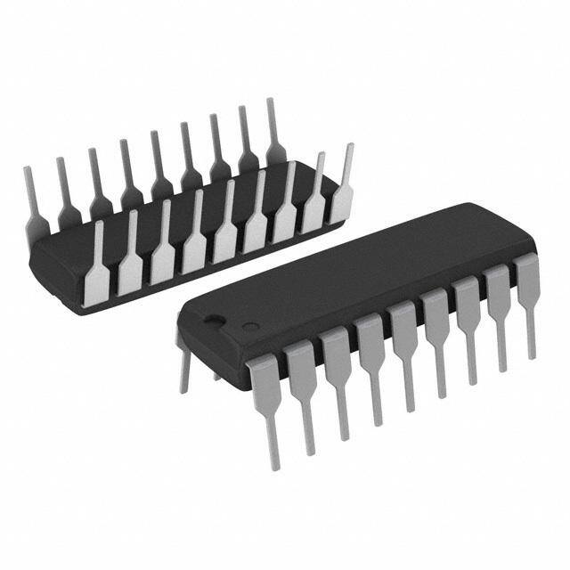
ICGOO电子元器件商城为您提供UC3871N由Texas Instruments设计生产,在icgoo商城现货销售,并且可以通过原厂、代理商等渠道进行代购。 UC3871N价格参考。Texas InstrumentsUC3871N封装/规格:PMIC - 照明,镇流器控制器, Fluorescent Lamp Controller Controller 57kHz ~ 78kHz No 18-PDIP。您可以下载UC3871N参考资料、Datasheet数据手册功能说明书,资料中有UC3871N 详细功能的应用电路图电压和使用方法及教程。
UC3871N是德州仪器(Texas Instruments)推出的一款专用照明控制芯片,属于PMIC中的镇流器控制器类别,主要用于驱动高强度气体放电灯(HID)和冷阴极荧光灯(CCFL)等照明系统。其典型应用场景包括汽车前大灯、高端车用照明系统以及工业或商业照明设备。

该芯片采用电流模式控制架构,具备高精度的电流调节能力,可实现稳定的灯管启动与运行控制。UC3871N支持升压(Boost)或半桥谐振转换器拓扑结构,适用于需要高压点火和恒功率运行的场合。在汽车应用中,常用于氙气大灯(HID Headlamps),能够提供快速启动、宽输入电压范围和良好的调光性能,提升行车安全性与照明质量。

此外,UC3871N集成多种保护功能,如过流保护、开路保护和短路保护,提高了系统可靠性。其工作温度范围较宽,适合在恶劣环境(如高温车载环境)中稳定运行。由于具备良好的动态响应和低待机功耗特性,也适用于对能效和稳定性要求较高的工业照明系统。

总之,UC3871N主要应用于需要高效、可靠镇流控制的高端照明场景,尤其在汽车HID大灯领域具有广泛使用价值。
| 参数 | 数值 |
| 产品目录 | 集成电路 (IC)半导体 |
| 描述 | IC FLUORESCENT LAMP DRVR 18-DIP显示驱动器和控制器 Resonant Fluorescent Lamp Driver |
| 产品分类 | |
| 品牌 | Texas Instruments |
| 产品手册 | |
| 产品图片 |
|
| rohs | 符合RoHS无铅 / 符合限制有害物质指令(RoHS)规范要求 |
| 产品系列 | 驱动器IC,显示驱动器和控制器,Texas Instruments UC3871N- |
| 数据手册 | |
| 产品型号 | UC3871N |
| 产品 | VFD Drivers |
| 产品目录页面 | |
| 产品种类 | 显示驱动器和控制器 |
| 供应商器件封装 | 18-PDIP |
| 其它名称 | 296-11327-5 |
| 制造商卷带宽度 | - |
| 制造商卷带材料 | - |
| 制造商卷带直径 | - |
| 包装 | 管件 |
| 单位重量 | 1.206 g |
| 商标 | Texas Instruments |
| 图号 | 296; 4040049; N; 18 |
| 安装类型 | 通孔 |
| 安装风格 | Through Hole |
| 封装 | Tube |
| 封装/外壳 | 18-DIP(0.300",7.62mm) |
| 封装/箱体 | PDIP-18 |
| 工作温度 | 0°C ~ 70°C |
| 工厂包装数量 | 20 |
| 最大工作温度 | + 70 C |
| 最小工作温度 | 0 C |
| 标准包装 | 20 |
| 电压-电源 | 4.5 V ~ 20 V |
| 电流-灌/拉输出 | - |
| 电流-电源 | 8mA |
| 类型 | 荧光灯控制器 |
| 系列 | UC3871 |
| 调光 | 无 |
| 频率 | 57kHz ~ 78kHz |


- 商务部:美国ITC正式对集成电路等产品启动337调查
- 曝三星4nm工艺存在良率问题 高通将骁龙8 Gen1或转产台积电
- 太阳诱电将投资9.5亿元在常州建新厂生产MLCC 预计2023年完工
- 英特尔发布欧洲新工厂建设计划 深化IDM 2.0 战略
- 台积电先进制程称霸业界 有大客户加持明年业绩稳了
- 达到5530亿美元!SIA预计今年全球半导体销售额将创下新高
- 英特尔拟将自动驾驶子公司Mobileye上市 估值或超500亿美元
- 三星加码芯片和SET,合并消费电子和移动部门,撤换高东真等 CEO
- 三星电子宣布重大人事变动 还合并消费电子和移动部门
- 海关总署:前11个月进口集成电路产品价值2.52万亿元 增长14.8%


PDF Datasheet 数据手册内容提取
UC1871 UC2871 UC3871 Resonant Fluorescent Lamp Driver FEATURES DESCRIPTION • 1m A ICC when Disabled The UC1871 Family of IC’s is optimized for highly efficient fluorescent lamp control. An additional PWM controller is integrated on the IC for applications re- • PWM Control for LCD Supply quiring an additional supply, as in LCD displays. When disabled the IC draws • Zero Voltage Switched (ZVS) on only 1m A, providing a true disconnect feature, which is optimum for battery Push-Pull Drivers powered systems. The switching frequency of all outputs are synchronized to the resonant frequency of the external passive network, which provides Zero • Open Lamp Detect Circuitry Voltage Switching on the Push-Pull drivers. • 4.5V to 20V Operation Soft-Start and open lamp detect circuitry have been incorporated to minimize • Non-saturating Transformer component stress. An open lamp is detected on the completion of a soft-start Topology cycle. • Smooth 100% Duty Cycle on The Buck controller is optimized for smooth duty cycle control to 100%, while Buck PWM and 0% to 95% on the flyback control ensures a maximum duty cycle of 95%. Flyback PWM Other features include a precision 1% reference, under voltage lockout, flyback current limit, and accurate minimum and maximum frequency control. BLOCK DIAGRAM Note: Pin numbers refer to DIL-18 and SOIC-18 packages only. UDG-92061-1 10/94
UC1871 UC2871 UC3871 ABSOLUTE MAXIMUM RATINGS Analog Inputs. . . . . . . . . . . . . . . . . . . . . . . . . - 0.3 to +10V Note 1: Currents are positive into, negative out of the specified ter- VCC, VC Voltage. . . . . . . . . . . . . . . . . . . . . . . . . . . . . +20V minal. Zero Detect Input Current Note 2: Consult Packaging Section of Databook for thermal High Impedance Source . . . . . . . . . . . . . . . . . . +10mA limitations and considerations of package. Zero Detect CONNECTION DIAGRAMS Low Impedance Source. . . . . . . . . . . . . . . . . . . . . +20V Power Dissipation at TA = 25(cid:176) C. . . . . . . . . . . . . . . . . . . 1W PLCC-20 (Top View) PACKAGE PIN FUNCTION Storage Temperature. . . . . . . . . . . . . . . . -65(cid:176) C to +150(cid:176) C Q Package FUNCTION PIN Lead Temperature . . . . . . . . . . . . . . . . . . . . . . . . . . 300(cid:176) C Gnd 1 B Out 2 DIL-18, SOIC-18 (TOP VIEW) A Out 3 J or N, DW Package VC 4 E/A 1 Comp 5 SS 6 E/A 1(-) 7 N/C 8 CT 9 Zero Detect 10 N/C 11 VREF 12 E/A 2(+) 13 E/A 2(-) 14 E/A 2 Comp 15 VCC 16 Enable 17 Flyback ISENSE 18 D Out 19 C Out 20 ELECTRICAL CHARACTERISTICS Unless otherwise stated, these parameters apply for TA = -55(cid:176) C to +125(cid:176) C for the UC1871; -25(cid:176) C to +85(cid:176) C for the UC2871; 0(cid:176) C to +70(cid:176) C for the UC3871; VCC = 5V, VC = 15V, VENABLE = 5V, CT = 1nF, Zero Det = 1V. PARAMETER TEST CONDITIONS MIN TYP MAX UNITS Reference Section Output Voltage TJ=25(cid:176) C 2.963 3.000 3.037 V Overtemp 2.940 3.000 3.060 V Line Regulation VCC = 4.75V to 18V 10 mV Load Regulation Io=0 to -5mA 10 mV Oscillator Section Free Running Freq TJ=25(cid:176) C 57 68 78 kHz Max Sync Frequency TJ=25(cid:176) C 160 200 240 kHz Charge Current VCT = 1.5V 180 200 220 m A Voltage Stability 2 % Temperature Stability 4 8 % Zero Detect Threshold 0.46 0.5 0.56 V Error Amp 1 Section Input Voltage VO = 2V 1.445 1.475 1.505 V Input Bias Current -0.4 -2 m A Open Loop Gain VO = 0.5 to 3V 65 90 dB Output High VEA(-) = 1.3V 3.1 3.5 3.9 V Output Low VEA(-) = 1.7V 0.1 0.2 V Output Source Current VEA(-) = 1.3V, Vo = 2V -350 -500 m A Output Sink Current VEA(-) = 1.7V, Vo = 2V 10 20 mA Common Mode Range 0 VIN-1V V Unity Gain Bandwidth TJ = 25(cid:176) C (Note 4) 1 MHz Maximum Source Impedance Note 5 100k W 2
UC1871 UC2871 UC3871 ELECTRICAL Unless otherwise stated, these parameters apply for TA = -55(cid:176) C to +125(cid:176) C for the UC1871; CHARACTERISTICS (cont.) -25(cid:176) C to +85(cid:176) C for the UC2871; 0(cid:176) C to +70(cid:176) C for the UC3871; VCC = 5V, VC = 15V, VENABLE = 5V, CT = 1nF, Zero Det = 1V. PARAMETER TEST CONDITIONS MIN TYP MAX UNITS Open Lamp Detect Section Soft Start Threshold VEA(-) = 0V 2.9 3.4 3.8 V Error Amp Threshold VSS = 4.2V 0.7 1.0 1.3 V Soft Start Current VSS = 2V 10 20 40 m A Error Amp 2 Section Input Offset Voltage VO = 2V 0 10 mV Input Bias Current -0.2 -1 m A Input Offset Current 0.5 m A Open Loop Gain VO = 0.5 to 3V 65 90 dB Output High VID = 100mV, VO = 2V 3.6 4 4.4 V Output Low VID = -100mv, VO = 2V 0.1 0.2 V Output Source Current VID = 100mV, VO = 2V -350 -500 m A Output Sink Current VID = -100mV, VO = 2V 10 20 mA Common Mode Range 0 VIN-2V V Unity Gain Bandwidth TJ = 25(cid:176) C (Note 4) 1 MHz Isense Section Threshold 0.475 0.525 0.575 V Output Section Output Low Level IOUT = 0, Outputs A and B 0.05 0.2 V IOUT = 10mA 0.1 0.4 V IOUT = 100mA 1.5 2.2 V Output High Level IOUT = 0, Outputs C and D 14.7 14.9 V IOUT = -10mA 13.5 14.3 V IOUT = -100mA 12.5 13.5 V Rise Time TJ = 25(cid:176) C, Cl = 1nF(Note 4) 30 80 ns Fall Time TJ = 25(cid:176) C, Cl = 1nF(Note 4) 30 80 ns Output Dynamics Out A and B Duty Cycle 48 49.9 50 % Out C Max Duty Cycle VEA1(-) = 1V 100 % Out C Min Duty Cycle VEA1(-) = 2V 0 % Out D Max Duty Cycle VEA2(+)- VEA2(-) = 100mV 92 96 % Out D Min Duty Cycle VEA2(+)- VEA2(-) = -100mV 0 % Under Voltage Lockout Section Start-Up Threshold 3.7 4.2 4.5 V Hysterisis 120 200 280 mV Enable Section Input High Threshold 2 V Input low Threshold 0.8 V Input Current VENABLE = 5V 150 400 m A Supply Current Section VCC Supply Current VCC = 20V 8 14 mA VC Supply Current VC=20V 7 12 mA ICC Disabled VCC = 20V, VENABLE = 0V 1 10 m A Note 3: Unless otherwise specified, all voltages are with respect to ground. Currents are positive into, and negative out of the specified terminal. Note 4: Guaranteed by design but not 100% tested in production. Note 5: Impedance below specified maximum guarantees proper operation of the Open Lamp Detect. 3
UC1871 UC2871 UC3871 TYPICAL APPLICATION Figure 1 APPLICATION INFORMATION Figure 1 shows a complete application circuit using the comparator senses the primary center-tap voltage, gen- UC3871 Resonant Fluorescent lamp and LCD driver. erating a synchronization pulse when the resonant wave- The IC provides all drive, control and housekeeping func- form falls to zero. The actual threshold is 0.5 volts, tions to implement CCFL and LCD converters. The buck providing a small amount of anticipation to offset propa- output voltage (transformer center-tap) provides the zero gation delay. crossing and synchronization signal. The LCD supply The synchronization pulse width is the time that the 4mA modulator is also synchronized to the resonant tank. current sink takes to discharge the timing capacitor to 0.1 The buck modulator drives a P-channel MOSFET di- volts. This pulse width sets the LCD supply modulator rectly, and operates over a 0-100% duty-cycle range. The minimum off time, and also limits the minimum linear modulation range includes 100%, allowing operation with control range of the buck modulator. The 200m A current minimal headroom. The LCD supply modulator also di- source charges the capacitor to a maximum of 3 volts. A rectly drives a P-channel MOSFET, but it’s duty-cycle is comparator blanks the zero detect signal until the capaci- limited to 95% to prevent flyback supply foldback. tor voltage exceeds 1 volt, preventing multiple synchroni- zation pulse generation and setting the maximum The oscillator and synchronization circuitry are shown in frequency. If the capacitor voltage reaches 3 volts (a zero Figure 2. The oscillator is designed to synchronize over a detection has not occurred) an internal clock pulse is 3:1 frequency range. In an actual application however, generated to limit the minimum frequency. the frequency range is only about 1.5:1. A zero detect 4
UC1871 UC2871 UC3871 APPLICATION INFORMATION (cont.) UC3871 Oscillator Section Figure 2 A unique protection feature incorporated in the UC3871 requirements. A logic level enable pin shuts down the IC, is the Open Lamp Detect circuit. An open lamp interrupts allowing direct connection to the battery. During shut- the current feedback loop and causes very high secon- down, the IC typically draws less than 1m A. The UC3871, dary voltage. Operation in this mode will usually break- operating from 4.5V to 20V, is compatible with almost all down the transformer’s insulation, causing permanent battery voltages used in portable computers. Under-volt- damage to the converter. The open lamp detect circuit, age lockout circuitry disables operation until sufficient shown in Figure 3 senses the lamp current feedback sig- supply voltage is available, and a 1% voltage reference nal at the error amplifiers input, and shuts down the out- insures accurate operation. Both inputs to the LCD sup- puts if insufficient signal is present. Soft-start circuitry ply error amplifier are uncommitted, allowing positive or limits initial turn-on currents and blanks the open lamp negative supply loop closure without additional circuitry. detect signal. The LCD supply modulator also incorporates cycle-by- cycle current limiting for added protection. Other features are included to minimize external circuitry UC1871 Open Lamp Detect Circuitry Figure 3 UNITRODE INTEGRATED CIRCUITS 7 CONTINENTAL BLVD. • MERRIMACK, NH 03054 TEL. (603) 424-2410 • FAX (603) 424-3460 5
PACKAGE OPTION ADDENDUM www.ti.com 29-May-2015 PACKAGING INFORMATION Orderable Device Status Package Type Package Pins Package Eco Plan Lead/Ball Finish MSL Peak Temp Op Temp (°C) Device Marking Samples (1) Drawing Qty (2) (6) (3) (4/5) 5962-9462201MVA OBSOLETE 18 TBD Call TI Call TI -55 to 125 5962-9462201Q2A OBSOLETE LCCC FK 20 TBD Call TI Call TI -55 to 125 UC1871J OBSOLETE CDIP J 18 TBD Call TI Call TI -55 to 125 UC1871J883B OBSOLETE CDIP J 18 TBD Call TI Call TI -55 to 125 UC1871L883B OBSOLETE TO/SOT L 20 TBD Call TI Call TI -55 to 125 UC2871DW ACTIVE SOIC DW 18 40 Green (RoHS CU NIPDAU Level-2-260C-1 YEAR -40 to 85 UC2871DW & no Sb/Br) UC2871DWG4 ACTIVE SOIC DW 18 40 Green (RoHS CU NIPDAU Level-2-260C-1 YEAR -40 to 85 UC2871DW & no Sb/Br) UC2871N LIFEBUY PDIP N 18 20 Green (RoHS CU NIPDAU N / A for Pkg Type -40 to 85 UC2871N & no Sb/Br) UC2871NG4 LIFEBUY PDIP N 18 20 Green (RoHS CU NIPDAU N / A for Pkg Type -40 to 85 UC2871N & no Sb/Br) UC3871DW ACTIVE SOIC DW 18 40 Green (RoHS CU NIPDAU Level-2-260C-1 YEAR 0 to 70 UC3871DW & no Sb/Br) UC3871DWG4 ACTIVE SOIC DW 18 40 Green (RoHS CU NIPDAU Level-2-260C-1 YEAR 0 to 70 UC3871DW & no Sb/Br) UC3871DWTR ACTIVE SOIC DW 18 2000 Green (RoHS CU NIPDAU Level-2-260C-1 YEAR 0 to 70 UC3871DW & no Sb/Br) UC3871N LIFEBUY PDIP N 18 20 Green (RoHS CU NIPDAU N / A for Pkg Type 0 to 70 UC3871N & no Sb/Br) UC3871NG4 LIFEBUY PDIP N 18 20 Green (RoHS CU NIPDAU N / A for Pkg Type 0 to 70 UC3871N & no Sb/Br) (1) The marketing status values are defined as follows: ACTIVE: Product device recommended for new designs. LIFEBUY: TI has announced that the device will be discontinued, and a lifetime-buy period is in effect. NRND: Not recommended for new designs. Device is in production to support existing customers, but TI does not recommend using this part in a new design. PREVIEW: Device has been announced but is not in production. Samples may or may not be available. OBSOLETE: TI has discontinued the production of the device. (2) Eco Plan - The planned eco-friendly classification: Pb-Free (RoHS), Pb-Free (RoHS Exempt), or Green (RoHS & no Sb/Br) - please check http://www.ti.com/productcontent for the latest availability information and additional product content details. TBD: The Pb-Free/Green conversion plan has not been defined. Addendum-Page 1
PACKAGE OPTION ADDENDUM www.ti.com 29-May-2015 Pb-Free (RoHS): TI's terms "Lead-Free" or "Pb-Free" mean semiconductor products that are compatible with the current RoHS requirements for all 6 substances, including the requirement that lead not exceed 0.1% by weight in homogeneous materials. Where designed to be soldered at high temperatures, TI Pb-Free products are suitable for use in specified lead-free processes. Pb-Free (RoHS Exempt): This component has a RoHS exemption for either 1) lead-based flip-chip solder bumps used between the die and package, or 2) lead-based die adhesive used between the die and leadframe. The component is otherwise considered Pb-Free (RoHS compatible) as defined above. Green (RoHS & no Sb/Br): TI defines "Green" to mean Pb-Free (RoHS compatible), and free of Bromine (Br) and Antimony (Sb) based flame retardants (Br or Sb do not exceed 0.1% by weight in homogeneous material) (3) MSL, Peak Temp. - The Moisture Sensitivity Level rating according to the JEDEC industry standard classifications, and peak solder temperature. (4) There may be additional marking, which relates to the logo, the lot trace code information, or the environmental category on the device. (5) Multiple Device Markings will be inside parentheses. Only one Device Marking contained in parentheses and separated by a "~" will appear on a device. If a line is indented then it is a continuation of the previous line and the two combined represent the entire Device Marking for that device. (6) Lead/Ball Finish - Orderable Devices may have multiple material finish options. Finish options are separated by a vertical ruled line. Lead/Ball Finish values may wrap to two lines if the finish value exceeds the maximum column width. Important Information and Disclaimer:The information provided on this page represents TI's knowledge and belief as of the date that it is provided. TI bases its knowledge and belief on information provided by third parties, and makes no representation or warranty as to the accuracy of such information. Efforts are underway to better integrate information from third parties. TI has taken and continues to take reasonable steps to provide representative and accurate information but may not have conducted destructive testing or chemical analysis on incoming materials and chemicals. TI and TI suppliers consider certain information to be proprietary, and thus CAS numbers and other limited information may not be available for release. In no event shall TI's liability arising out of such information exceed the total purchase price of the TI part(s) at issue in this document sold by TI to Customer on an annual basis. OTHER QUALIFIED VERSIONS OF UC1871, UC3871 : •Catalog: UC3871 •Military: UC1871 NOTE: Qualified Version Definitions: •Catalog - TI's standard catalog product •Military - QML certified for Military and Defense Applications Addendum-Page 2
PACKAGE MATERIALS INFORMATION www.ti.com 14-Jul-2012 TAPE AND REEL INFORMATION *Alldimensionsarenominal Device Package Package Pins SPQ Reel Reel A0 B0 K0 P1 W Pin1 Type Drawing Diameter Width (mm) (mm) (mm) (mm) (mm) Quadrant (mm) W1(mm) UC3871DWTR SOIC DW 18 2000 330.0 24.4 10.9 12.0 2.7 12.0 24.0 Q1 PackMaterials-Page1
PACKAGE MATERIALS INFORMATION www.ti.com 14-Jul-2012 *Alldimensionsarenominal Device PackageType PackageDrawing Pins SPQ Length(mm) Width(mm) Height(mm) UC3871DWTR SOIC DW 18 2000 367.0 367.0 45.0 PackMaterials-Page2
None
None
None
None
IMPORTANTNOTICE TexasInstrumentsIncorporatedanditssubsidiaries(TI)reservetherighttomakecorrections,enhancements,improvementsandother changestoitssemiconductorproductsandservicesperJESD46,latestissue,andtodiscontinueanyproductorserviceperJESD48,latest issue.Buyersshouldobtainthelatestrelevantinformationbeforeplacingordersandshouldverifythatsuchinformationiscurrentand complete.Allsemiconductorproducts(alsoreferredtohereinas“components”)aresoldsubjecttoTI’stermsandconditionsofsale suppliedatthetimeoforderacknowledgment. TIwarrantsperformanceofitscomponentstothespecificationsapplicableatthetimeofsale,inaccordancewiththewarrantyinTI’sterms andconditionsofsaleofsemiconductorproducts.TestingandotherqualitycontroltechniquesareusedtotheextentTIdeemsnecessary tosupportthiswarranty.Exceptwheremandatedbyapplicablelaw,testingofallparametersofeachcomponentisnotnecessarily performed. TIassumesnoliabilityforapplicationsassistanceorthedesignofBuyers’products.Buyersareresponsiblefortheirproductsand applicationsusingTIcomponents.TominimizetherisksassociatedwithBuyers’productsandapplications,Buyersshouldprovide adequatedesignandoperatingsafeguards. TIdoesnotwarrantorrepresentthatanylicense,eitherexpressorimplied,isgrantedunderanypatentright,copyright,maskworkright,or otherintellectualpropertyrightrelatingtoanycombination,machine,orprocessinwhichTIcomponentsorservicesareused.Information publishedbyTIregardingthird-partyproductsorservicesdoesnotconstitutealicensetousesuchproductsorservicesorawarrantyor endorsementthereof.Useofsuchinformationmayrequirealicensefromathirdpartyunderthepatentsorotherintellectualpropertyofthe thirdparty,oralicensefromTIunderthepatentsorotherintellectualpropertyofTI. ReproductionofsignificantportionsofTIinformationinTIdatabooksordatasheetsispermissibleonlyifreproductioniswithoutalteration andisaccompaniedbyallassociatedwarranties,conditions,limitations,andnotices.TIisnotresponsibleorliableforsuchaltered documentation.Informationofthirdpartiesmaybesubjecttoadditionalrestrictions. ResaleofTIcomponentsorserviceswithstatementsdifferentfromorbeyondtheparametersstatedbyTIforthatcomponentorservice voidsallexpressandanyimpliedwarrantiesfortheassociatedTIcomponentorserviceandisanunfairanddeceptivebusinesspractice. TIisnotresponsibleorliableforanysuchstatements. Buyeracknowledgesandagreesthatitissolelyresponsibleforcompliancewithalllegal,regulatoryandsafety-relatedrequirements concerningitsproducts,andanyuseofTIcomponentsinitsapplications,notwithstandinganyapplications-relatedinformationorsupport thatmaybeprovidedbyTI.Buyerrepresentsandagreesthatithasallthenecessaryexpertisetocreateandimplementsafeguardswhich anticipatedangerousconsequencesoffailures,monitorfailuresandtheirconsequences,lessenthelikelihoodoffailuresthatmightcause harmandtakeappropriateremedialactions.BuyerwillfullyindemnifyTIanditsrepresentativesagainstanydamagesarisingoutoftheuse ofanyTIcomponentsinsafety-criticalapplications. Insomecases,TIcomponentsmaybepromotedspecificallytofacilitatesafety-relatedapplications.Withsuchcomponents,TI’sgoalisto helpenablecustomerstodesignandcreatetheirownend-productsolutionsthatmeetapplicablefunctionalsafetystandardsand requirements.Nonetheless,suchcomponentsaresubjecttotheseterms. NoTIcomponentsareauthorizedforuseinFDAClassIII(orsimilarlife-criticalmedicalequipment)unlessauthorizedofficersoftheparties haveexecutedaspecialagreementspecificallygoverningsuchuse. OnlythoseTIcomponentswhichTIhasspecificallydesignatedasmilitarygradeor“enhancedplastic”aredesignedandintendedforusein military/aerospaceapplicationsorenvironments.BuyeracknowledgesandagreesthatanymilitaryoraerospaceuseofTIcomponents whichhavenotbeensodesignatedissolelyattheBuyer'srisk,andthatBuyerissolelyresponsibleforcompliancewithalllegaland regulatoryrequirementsinconnectionwithsuchuse. TIhasspecificallydesignatedcertaincomponentsasmeetingISO/TS16949requirements,mainlyforautomotiveuse.Inanycaseofuseof non-designatedproducts,TIwillnotberesponsibleforanyfailuretomeetISO/TS16949. Products Applications Audio www.ti.com/audio AutomotiveandTransportation www.ti.com/automotive Amplifiers amplifier.ti.com CommunicationsandTelecom www.ti.com/communications DataConverters dataconverter.ti.com ComputersandPeripherals www.ti.com/computers DLP®Products www.dlp.com ConsumerElectronics www.ti.com/consumer-apps DSP dsp.ti.com EnergyandLighting www.ti.com/energy ClocksandTimers www.ti.com/clocks Industrial www.ti.com/industrial Interface interface.ti.com Medical www.ti.com/medical Logic logic.ti.com Security www.ti.com/security PowerMgmt power.ti.com Space,AvionicsandDefense www.ti.com/space-avionics-defense Microcontrollers microcontroller.ti.com VideoandImaging www.ti.com/video RFID www.ti-rfid.com OMAPApplicationsProcessors www.ti.com/omap TIE2ECommunity e2e.ti.com WirelessConnectivity www.ti.com/wirelessconnectivity MailingAddress:TexasInstruments,PostOfficeBox655303,Dallas,Texas75265 Copyright©2015,TexasInstrumentsIncorporated