ICGOO在线商城 > 集成电路(IC) > PMIC - PFC(功率因数修正) > UC3854DW
 Datasheet下载
- 型号: UC3854DW
- 制造商: Texas Instruments
- 库位|库存: xxxx|xxxx
- 要求:
| 数量阶梯 | 香港交货 | 国内含税 |
| +xxxx | $xxxx | ¥xxxx |
查看当月历史价格
查看今年历史价格
UC3854DW产品简介:
ICGOO电子元器件商城为您提供UC3854DW由Texas Instruments设计生产,在icgoo商城现货销售,并且可以通过原厂、代理商等渠道进行代购。 UC3854DW价格参考¥10.99-¥22.52。Texas InstrumentsUC3854DW封装/规格:PMIC - PFC(功率因数修正), PFC IC Average Current 200kHz 16-SOIC。您可以下载UC3854DW参考资料、Datasheet数据手册功能说明书,资料中有UC3854DW 详细功能的应用电路图电压和使用方法及教程。
UC3854DW是由Texas Instruments(德州仪器)生产的一款PMIC - PFC(功率因数校正)芯片,广泛应用于高效率电源设计中。以下是其主要应用场景:

1. 工业设备:适用于工业自动化设备中的高效电源系统,例如可编程逻辑控制器(PLC)、伺服驱动器和变频器等。这些设备需要稳定的高功率输入,而UC3854DW可以有效提高功率因数并降低谐波失真。

2. 通信电源:在基站、路由器和其他通信设备的电源模块中,UC3854DW用于实现高效的功率转换,确保设备在不同负载条件下的稳定运行。

3. 消费电子:大功率家用电器如空调、洗衣机和冰箱等,需要PFC电路来满足能效标准。UC3854DW能够提供精确的控制,优化家电的能源使用效率。

4. 不间断电源(UPS):在UPS系统中,该芯片帮助实现更高效的功率转换,延长电池寿命,并减少能量损耗。

5. 新能源领域:在太阳能逆变器和风力发电系统中,UC3854DW用于提升功率因数,改善电网兼容性,同时提高整体系统的效率。

6. 电动车辆充电站:为电动车充电站提供高效且可靠的功率因数校正解决方案,确保快速充电的同时减少对电网的影响。

UC3854DW通过其先进的控制算法和高集成度特性,在上述应用中表现出色,能够显著提升系统的性能和效率。
| 参数 | 数值 |
| 产品目录 | 集成电路 (IC)半导体 |
| 描述 | IC PFC CTRLR AVERAGE CURR 16SOIC功率因数校正 - PFC Pwr Factor Pre- |
| 产品分类 | |
| 品牌 | Texas Instruments |
| 产品手册 | |
| 产品图片 |
|
| rohs | 符合RoHS无铅 / 符合限制有害物质指令(RoHS)规范要求 |
| 产品系列 | 电源管理 IC,功率因数校正 - PFC,Texas Instruments UC3854DW- |
| 数据手册 | |
| 产品型号 | UC3854DW |
| 产品目录页面 | |
| 产品种类 | 功率因数校正 - PFC |
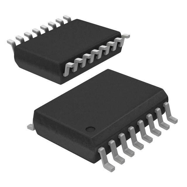
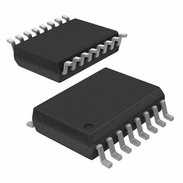
| 供应商器件封装 | 16-SOIC |
| 其它名称 | 296-11312-5 |
| 包装 | 管件 |
| 单位重量 | 473.700 mg |
| 商标 | Texas Instruments |
| 安装类型 | 表面贴装 |
| 安装风格 | SMD/SMT |
| 封装 | Tube |
| 封装/外壳 | 16-SOIC(0.295",7.50mm 宽) |
| 封装/箱体 | SOIC-16 |
| 工作温度 | 0°C ~ 70°C |
| 工厂包装数量 | 40 |
| 开关频率 | 118 kHz |
| 最大工作温度 | + 70 C |
| 最小工作温度 | 0 C |
| 标准包装 | 40 |
| 模式 | 平均电流 |
| 电压-电源 | 14.5 V ~ 30 V |
| 电流-启动 | 1.5mA |
| 系列 | UC3854 |
| 频率-开关 | 200kHz |

.jpg)


- 商务部:美国ITC正式对集成电路等产品启动337调查
- 曝三星4nm工艺存在良率问题 高通将骁龙8 Gen1或转产台积电
- 太阳诱电将投资9.5亿元在常州建新厂生产MLCC 预计2023年完工
- 英特尔发布欧洲新工厂建设计划 深化IDM 2.0 战略
- 台积电先进制程称霸业界 有大客户加持明年业绩稳了
- 达到5530亿美元!SIA预计今年全球半导体销售额将创下新高
- 英特尔拟将自动驾驶子公司Mobileye上市 估值或超500亿美元
- 三星加码芯片和SET,合并消费电子和移动部门,撤换高东真等 CEO
- 三星电子宣布重大人事变动 还合并消费电子和移动部门
- 海关总署:前11个月进口集成电路产品价值2.52万亿元 增长14.8%


PDF Datasheet 数据手册内容提取
Product Order Technical Tools & Support & Folder Now Documents Software Community UC1854,UC2854,UC3854 SLUS336A–JUNE1998–REVISEDDECEMBER2016 UCx854 High-Power Factor Preregulator 1 Features In addition, the UC1854 contains a power MOSFET- compatible gate driver, 7.5-V reference, line • ControlBoostPWMto0.99PowerFactor 1 anticipator, load-enable comparator, low-supply • LimitLine-CurrentDistortionto<5% detector,andovercurrentcomparator. • World-WideOperationWithoutSwitches The UC1854 uses average current-mode control to • FeedforwardLineRegulation accomplish fixed-frequency current control with • AverageCurrent-ModeControl stability and low distortion. Unlike peak current-mode, average current control accurately maintains • LowNoiseSensitivity sinusoidal line current without slope compensation • LowStartupSupplyCurrent andwithminimalresponsetonoisetransients. • Fixed-FrequencyPWMDrive The high reference voltage and high oscillator • Low-OffsetAnalogMultiplierandDivider amplitude of the UC1854 minimize noise sensitivity • 1-ATotem-PoleGateDriver while fast PWM elements permit chopping frequencies above 200 kHz. The UC1854 is used in • PrecisionVoltageReference single-phase and three-phase systems with line voltages that vary from 75 V to 275 V and line 2 Applications frequencies across the 50-Hz to 400-Hz range. To • OfflineAC-to-DCConverters reducetheburdenonthecircuitrythatsuppliespower to this device, the UC1854 features low starting • Medical,Industrial,Telecom,andITPower supplycurrent. Supplies • UninterruptiblePowerSupplies(UPS) These devices are available packaged in 16-pin plastic and ceramic dual in-line packages, and a • AppliancesandWhiteGoods varietyofsurface-mountpackages. 3 Description DeviceInformation(1) The UC1854 provides active-power factor correction PARTNUMBER PACKAGE BODYSIZE(NOM) for power systems that otherwise would draw non- SOIC(16) 7.50mm×10.30mm sinusoidal current from sinusoidal power lines. This device implements all the control functions necessary UC1854,UC2854, PLCC(20) 8.96mm×8.96mm to build a power supply capable of optimally using UC3854 CDIP(16) 6.92mm×19.56mm available power-line current while minimizing line- PDIP(16) 6.35mm×19.30mm current distortion. To do this, the UC1854 contains a (1) For all available packages, see the orderable addendum at voltage amplifier, an analog multiplier and divider, a theendofthedatasheet. currentamplifier,andafixed-frequencyPWM. BlockDiagram Line EMI Input Filter – + V40O0U VTDC VREF VCC 10 2 5 4 3 16 VREF ENA PKLMT MULTOUT ISENSE CAOUT GTDRV VSENSE 11 6 IAC UC3854 8 VRMS VAOUT 7 VCC CT SS RSET GND VREF 15 14 13 12 1 9 VCC VREF Copyright © 2016,Texas Instruments Incorporated 1 An IMPORTANT NOTICE at the end of this data sheet addresses availability, warranty, changes, use in safety-critical applications, intellectualpropertymattersandotherimportantdisclaimers.PRODUCTIONDATA.
UC1854,UC2854,UC3854 SLUS336A–JUNE1998–REVISEDDECEMBER2016 www.ti.com Table of Contents 1 Features.................................................................. 1 8.4 DeviceFunctionalModes........................................11 2 Applications........................................................... 1 9 ApplicationandImplementation........................ 12 3 Description............................................................. 1 9.1 ApplicationInformation............................................12 4 RevisionHistory..................................................... 2 9.2 TypicalApplication..................................................12 5 DeviceComparisonTable..................................... 3 10 PowerSupplyRecommendations..................... 16 6 PinConfigurationandFunctions......................... 3 11 Layout................................................................... 16 11.1 LayoutGuidelines.................................................16 7 Specifications......................................................... 5 11.2 LayoutExample....................................................17 7.1 AbsoluteMaximumRatings......................................5 12 DeviceandDocumentationSupport................. 18 7.2 ESDRatings..............................................................5 7.3 RecommendedOperatingConditions.......................6 12.1 DocumentationSupport........................................18 7.4 ThermalInformation..................................................6 12.2 RelatedLinks........................................................18 7.5 ElectricalCharacteristics...........................................6 12.3 ReceivingNotificationofDocumentationUpdates18 7.6 TypicalCharacteristics..............................................8 12.4 CommunityResources..........................................18 12.5 Trademarks...........................................................18 8 DetailedDescription............................................ 10 12.6 ElectrostaticDischargeCaution............................18 8.1 Overview.................................................................10 12.7 Glossary................................................................18 8.2 FunctionalBlockDiagram.......................................10 13 Mechanical,Packaging,andOrderable 8.3 FeatureDescription.................................................11 Information........................................................... 18 4 Revision History NOTE:Pagenumbersforpreviousrevisionsmaydifferfrompagenumbersinthecurrentversion. ChangesfromOriginal(June1998)toRevisionA Page • AddedApplicationssection,DeviceInformationtable,PinConfigurationandFunctionssection,Specifications section,ESDRatingstable,RecommendedOperatingConditionstable,DetailedDescriptionsection,Application andImplementationsection,PowerSupplyRecommendationssection,Layoutsection,DeviceandDocumentation Supportsection,andMechanical,Packaging,andOrderableInformationsection................................................................ 1 • AddedThermalInformationtable........................................................................................................................................... 6 • ChangedIACvalueinbothMultiplierOutputvsMultiplierInputsimagesfrommAtoµA. ................................................... 8 2 SubmitDocumentationFeedback Copyright©1998–2016,TexasInstrumentsIncorporated ProductFolderLinks:UC1854 UC2854 UC3854
UC1854,UC2854,UC3854 www.ti.com SLUS336A–JUNE1998–REVISEDDECEMBER2016 5 Device Comparison Table PARAMETER UC3854 UC3854A UC3854B Supplycurrent,OFF 2-mAmaximum 400-µAmaximum 400-µAmaximum Supplyvoltage(V ) 35-Vmaximum 22-Vmaximum 22-Vmaximum CC VCCturn-onthreshold 16-Vtypical 16-Vtypical 10.5-Vtypical VCCUVLOhysteresis 6-Vtypical 6-Vtypical 0.5-Vtypical Currentamplifierbandwidth 1-MHztypical 5-MHztypical 5-MHztypical Currentamplifieroffset 4-mV,–4-mVmaximum 0-mV,–4-mVmaximum 0-mV,–4-mVmaximum MULTOUTvoltage(high) 2.5-Vtypical 5-Vtypical 5-Vtypical Multipliergaintolerance Notspecified –0.9to–1.1 –0.9to–1.1 ENABLEpropagationdelay Notspecified 300-nstypical 300-nstypical VSENSEinput 7.5V 3V 3V IACvoltage 6-Vtypical 0.5-Vtypical 0.5-Vtypical Voltageamplifierclamp — Internal Internal Currentamplifierclamp — Internal Internal VREFgoodcircuitry — Internal Internal 6 Pin Configuration and Functions DW,J,andNPackages FNPackage 16-PinSOIC,CDIP,andPDIP 20-PinPLCC TopView TopView T V M R GND 1 16 GTDRV PKL GND NC GTD VCC PKLMT 2 15 VCC CAOUT 3 14 CT 3 2 1 0 9 2 1 ISENSE 4 13 SS CAOUT 4 18 CT MULTOUT 5 12 RSET ISENSE 5 17 SS IAC 6 11 VSENSE NC 6 16 NC VAOUT 7 10 ENA MULTOUT 7 15 RSET VRMS 8 9 VREF IAC 8 14 VSENSE 0 1 2 3 9 1 1 1 1 Not to scale Not to scale T S C F A U M N E N O R R E A V V V Copyright©1998–2016,TexasInstrumentsIncorporated SubmitDocumentationFeedback 3 ProductFolderLinks:UC1854 UC2854 UC3854
UC1854,UC2854,UC3854 SLUS336A–JUNE1998–REVISEDDECEMBER2016 www.ti.com PinFunctions PIN CDIP, I/O DESCRIPTION NAME PDIP, PLCC SOIC Currentamplifieroutput.Thisistheoutputofawide-bandwidthoperationalamplifierthatsensesline currentandcommandsthepulse-widthmodulator(PWM)toforcethecorrectcurrent.Thisoutput CAOUT 3 4 O swingsclosetoGND,allowingthePWMtoforcezerodutycyclewhennecessary.Thecurrent amplifierremainsactiveeveniftheICisdisabled.Thecurrent-amplifieroutputstageisanNPN emitter-followerpullupandan8-kΩresistortoground. Oscillatortimingcapacitor.AcapacitorfromCTtoGNDsetsthePWMoscillatorfrequency. UseEquation1: CT 14 18 I 1.25 F= R ´C SET T (1) Enable.ENAisalogicinputthatenablesthePWMoutput,voltagereference,andoscillator.ENA alsoreleasesthesoft-startclamp,allowingSStorise.Whennotinuse,connectENAtoa5-Vsupply ENA 10 13 I orpullENAhighwitha22-kΩresistor.TheENApinisnotintendedtobeusedasahighspeed shutdowntothePWMoutput. Ground.AllvoltagesaremeasuredwithrespecttoGND.VCCandVREFmustbebypasseddirectly toGNDwithan0.1-µForlargerceramiccapacitor.Thetimingcapacitordischargecurrentalso GND 1 2 — returnstothispin,sotheleadfromtheoscillatortimingcapacitortoGNDmustalsobeasshortand asdirectaspossible. Gatedrive.TheoutputofthePWMisatotem-poleMOSFETgatedriveronGTDRV.Thisoutputis internallyclampedto15VsothattheICoperateswithV ashighas35V.Useaseriesgate CC GTDRV 16 20 O resistorofatleast5ΩtopreventinteractionbetweenthegateimpedanceandtheGTDRVoutput driverthatmightcausetheGTDRVoutputtoovershootexcessively.SomeovershootoftheGTDRV outputisalwaysexpectedwhendrivingacapacitiveload. InputACcurrent.Thisinputtotheanalogmultiplierisacurrent.Themultiplieristailoredforverylow distortionfromthiscurrentinput(IAC)toMULTOUT,thisistheonlymultiplierinputthatmustbeused forsensinginstantaneouslinevoltage.ThenominalvoltageonIACis6V,inadditiontoaresistor IAC 6 8 I fromIACtorectified60Hz,connectaresistorfromIACtoREF.IftheresistortoVREFisone-fourth ofthevalueoftheresistortotherectifier,thenthe6-Voffsetiscancelled,andthelinecurrenthas minimalcross-overdistortion. Current-senseminus.Thisistheinvertinginputtothecurrentamplifier.Thisinputandthenon- ISENSE 4 5 I invertinginput,MULTOUT,remainfunctionaldowntoandbelowGND.Takecaretoavoidtaking theseinputsbelow–0.5VbecausetheyareprotectedwithdiodestoGND. Multiplieroutputandcurrent-senseplus.Theoutputoftheanalogmultiplierandthenon-inverting inputofthecurrentamplifierareconnectedtogetheratMULTOUT.Thecautionsabouttaking MULTOUT 5 7 I/O ISENSEbelow–0.5ValsoapplytoMULTOUT.Asthemultiplieroutputisacurrent,thisisahigh- impedanceinputsimilartoISENSE,sothecurrentamplifiercanbeconfiguredasadifferential amplifiertorejectGNDnoise.Figure9showsanexampleofusingthecurrentamplifierdifferentially. 1,6, NC — — Noconnection 11,16 Peakcurrentlimit.ThethresholdforPKLMTis0V.Connectthisinputtothenegativevoltageonthe PKLMT 2 3 I current-senseresistorasshowninFigure9.UsearesistortoVREFtooffsetthenegativecurrent- sensesignaluptoGND. Oscillatorchargingcurrentandmultiplierlimitset.AresistorfromRSETtoGNDprogramsoscillator RSET 12 15 I chargingcurrentandmaximummultiplieroutput.Multiplieroutputcurrentdoesnotexceed3.75V dividedbytheresistorfromRSETtoGND. Softstart.SSremainsatGNDaslongasthedeviceisdisabledorV istoolow.SSpullsupto CC over8Vbyaninternal14-mAcurrentsourcewhenbothV becomesvalidandtheICisenabled. CC SSactsasthereferenceinputtothevoltageamplifierifSSisbelowVREF.Withalargecapacitor SS 13 17 I fromSStoGND,thereferencetothevoltageregulatingamplifierrisesslowly,andincreasesthe PWMdutycycleslowly.Intheeventofadisablecommandorasupplydropout,SSquickly dischargestogroundanddisablesthePWM. Voltageamplifieroutput.Thisistheoutputoftheoperationalamplifierthatregulatesoutputvoltage. Likethecurrentamplifier,thevoltageamplifierremainsactiveeveniftheICisdisabledwitheither ENAorVCC.Thismeansthatlargefeedbackcapacitorsacrosstheamplifierstaychargedthrough VAOUT 7 9 O momentarydisablecycles.Voltageamplifieroutputlevelsbelow1Vinhibitmultiplieroutput.The voltageamplifieroutputisinternallylimitedtoapproximately5.8Vtopreventovershoot.Thevoltage amplifieroutputstageisanNPNemitter-followerpullupandan8-kΩresistortoground. 4 SubmitDocumentationFeedback Copyright©1998–2016,TexasInstrumentsIncorporated ProductFolderLinks:UC1854 UC2854 UC3854
UC1854,UC2854,UC3854 www.ti.com SLUS336A–JUNE1998–REVISEDDECEMBER2016 PinFunctions(continued) PIN CDIP, I/O DESCRIPTION NAME PDIP, PLCC SOIC Positivesupplyvoltage.ConnectVCCtoastablesourceofatleast20mAabove17Vfornormal operation.AlsobypassVCCdirectlytoGNDtoabsorbsupplycurrentspikesrequiredtocharge VCC 15 19 — externalMOSFETgatecapacitances.TopreventinadequateGTDRVsignals,thesedevicesare inhibitedunlessV exceedstheupperundervoltage-lockoutthresholdandremainsabovethelower CC threshold. Voltagereferenceoutput.VREFistheoutputofanaccurate7.5-Vvoltagereference.Thisoutputis capableofdelivering10mAtoperipheralcircuitryandisinternallyshort-circuitcurrentlimited.VREF VREF 9 12 O isdisabledandremainsat0VwhenV isloworwhenENAislow.BypassVREFtoGNDwithan CC 0.1-µForlargerceramiccapacitorforbeststability. RMSlinevoltage.TheoutputofaboostPWMisproportionaltotheinputvoltage,sowhentheline voltageintoalow-bandwidthboostPWM-voltageregulatorchanges,theoutputchangesimmediately VRMS 8 10 I andslowlyrecoverstotheregulatedlevel.Forthesedevices,theVRMSinputcompensatesforline voltagechangesifitisconnectedtoavoltageproportionaltotheRMSinputlinevoltage.Forbest control,theVRMSvoltagemuststaybetween1.5Vand3.5V. Voltageamplifierinvertinginput.Thisisnormallyconnectedtoafeedbacknetworkandtotheboost VSENSE 11 14 I converteroutputthroughadividernetwork. 7 Specifications 7.1 Absolute Maximum Ratings overoperatingfree-airtemperaturerange(unlessotherwisenoted)(1)(2)(3)(4)(5) MIN MAX UNIT Supplyvoltage VCC 35 V VSENSE,VRMS 11 InputVoltage ISENSE,MULTOUT 11 V PKLMT 5 50%dutycycle 1.5 GatedrivercurrentInputcurrent A Continuous 0.5 Inputcurrent RSET,IAC,PKLMT,ENA 10 mA Powerdissipation 1 W Storagetemperature,T –65 150 °C stg (1) StressesbeyondthoselistedunderAbsoluteMaximumRatingsmaycausepermanentdamagetothedevice.Thesearestressratings only,whichdonotimplyfunctionaloperationofthedeviceattheseoranyotherconditionsbeyondthoseindicatedunderRecommended OperatingConditions.Exposuretoabsolute-maximum-ratedconditionsforextendedperiodsmayaffectdevicereliability. (2) AllvoltageswithrespecttoGND. (3) Allcurrentsarepositiveintothespecifiedterminal. (4) ENAinputisinternallyclampedtoapproximately14V. (5) ConsultUnitrodeIntegratedCircuitsdatabookforinformationregardingthermalspecificationsandlimitations. 7.2 ESD Ratings VALUE UNIT Human-bodymodel(HBM),perANSI/ESDA/JEDECJS-001(1) ±2500 V Electrostaticdischarge V (ESD) Charged-devicemodel(CDM),perJEDECspecificationJESD22-C101(2) ±1500 (1) JEDECdocumentJEP155statesthat500-VHBMallowssafemanufacturingwithastandardESDcontrolprocess. (2) JEDECdocumentJEP157statesthat250-VCDMallowssafemanufacturingwithastandardESDcontrolprocess. Copyright©1998–2016,TexasInstrumentsIncorporated SubmitDocumentationFeedback 5 ProductFolderLinks:UC1854 UC2854 UC3854
UC1854,UC2854,UC3854 SLUS336A–JUNE1998–REVISEDDECEMBER2016 www.ti.com 7.3 Recommended Operating Conditions overoperatingfree-airtemperaturerange(unlessotherwisenoted) MIN MAX UNIT V Supplyvoltage 10 20 CC UC1854 –55 125 T Operatingjunctiontemperature UC2854 –40 85 °C J UC3854 0 70 7.4 Thermal Information UCx854 THERMALMETRIC(1) DW(SOIC) FN(PLCC) J(CDIP) N(PDIP) UNIT 16PINS 20PINS 16PINS 16PINS R Junction-to-ambientthermalresistance 71.5 — 25 40.8 °C/W θJA R Junction-to-case(top)thermalresistance 32.7 — — 26.8 °C/W θJC(top) R Junction-to-boardthermalresistance 36.3 — 5.5 20.9 °C/W θJB ψ Junction-to-topcharacterizationparameter 6.8 — 2.1 10.9 °C/W JT Junction-to-boardcharacterization ψ 35.8 — 5.4 20.7 °C/W JB parameter Junction-to-case(bottom)thermal R — — 3.4 — °C/W θJC(bot) resistance (1) Formoreinformationabouttraditionalandnewthermalmetrics,seetheSemiconductorandICPackageThermalMetricsapplication report. 7.5 Electrical Characteristics Unlessotherwisestated,V =18V,R =15kΩtoground,C =1.5nFtoground,V =1V,V =7.5V, CC SET T PKLMT ENA V =1.5V,I =100µA,V =0V,V =3.5V,V =5V,V =7.5V,noloadonSS,CAOUT,VAOUT, RMS AC ISENSE CAOUT VAOUT SENSE VREF,GTDRV,T =T,T =–55°Cto125°CfortheUC1854,T =–40°Cto85°CfortheUC2854, A J A A andT =0°Cto70°CfortheUC3854. A PARAMETER TESTCONDITIONS MIN TYP MAX UNIT OVERALL Supplycurrent,OFF V =0V 1.5 2 mA ENA Supplycurrent,ON 10 16 mA V turn-onthreshold 14.5 16 17.5 V CC V turn-offthreshold 9 10 11 V CC ENAthreshold,rising 2.4 2.55 2.7 V ENAthresholdhysteresis 0.2 0.25 0.3 V ENAinputcurrent V =0V –5 –0.2 5 µA ENA V inputcurrent V =5V –1 –0.01 1 µA RMS RMS VOLTAGEAMPLIFIER Voltageamplifieroffsetvoltage V =5V –8 8 mV VAOUT VSENSEbiascurrent –500 –25 500 nA Voltageamplifiergain 70 100 dB Voltageamplifieroutputswing 0.5 5.8 V Voltageamplifiershortcircuitcurrent V =0V –36 –20 –5 mA VAOUT SScurrent V =2.5V –20 –14 –6 µA SS CURRENTAMPLIFIER Currentamplifieroffsetvoltage –4 4 mV ISENSEbiascurrent –500 –120 500 nA Inputrange(ISENSE,MULTOUT) –0.3 2.5 V Currentamplifiergain 80 110 dB 6 SubmitDocumentationFeedback Copyright©1998–2016,TexasInstrumentsIncorporated ProductFolderLinks:UC1854 UC2854 UC3854
UC1854,UC2854,UC3854 www.ti.com SLUS336A–JUNE1998–REVISEDDECEMBER2016 Electrical Characteristics (continued) Unlessotherwisestated,V =18V,R =15kΩtoground,C =1.5nFtoground,V =1V,V =7.5V, CC SET T PKLMT ENA V =1.5V,I =100µA,V =0V,V =3.5V,V =5V,V =7.5V,noloadonSS,CAOUT,VAOUT, RMS AC ISENSE CAOUT VAOUT SENSE VREF,GTDRV,T =T,T =–55°Cto125°CfortheUC1854,T =–40°Cto85°CfortheUC2854, A J A A andT =0°Cto70°CfortheUC3854. A PARAMETER TESTCONDITIONS MIN TYP MAX UNIT Currentamplifieroutputswing 0.5 16 V Currentamplifiershort-circuitcurrent V =0V –36 –20 –5 mA CAOUT Currentamplifiergain–bandwidth T =25°C(1) 400 800 kHz product A REFERENCE Referenceoutputvoltage I =0mA,T =25°C 7.4 7.5 7.6 V REF A Referenceoutputvoltage I =0mA,overtemperature 7.35 7.5 7.65 V REF VREFloadregulation –10mA<I <0mA –15 5 15 mV REF VREFlineregulation 15V<V <35V –10 2 10 mV CC VREFshortcircuitcurrent V =0V –50 –28 –12 mA REF MULTIPLIER MultiplieroutcurrentIAClimited I =100µA,R =10kΩ,V =1.25V –220 –200 –180 µA AC SET RMS Multiplieroutcurrentzero I =0µA,R =15kΩ –2 –0.2 –2 µA AC SET I =450µA,R =15kΩ,V =1V, MultiplieroutcurrentRSETlimited AC SET RMS –280 –255 –220 µA V =6V VAOUT Multiplieroutcurrent I =50µA,V =2V,V =4V –50 –42 –33 µA AC RMS VAOUT Multiplieroutcurrent I =100µA,V =2V,V =2V –38 –27 –12 µA AC RMS VAOUT Multiplieroutcurrent I =200µA,V =2V,V =4V –165 –150 –105 µA AC RMS VAOUT Multiplieroutcurrent I =300µA,V =1V,V =2V –250 –225 –150 µA AC RMS VAOUT Multiplieroutcurrent I =100µA,V =1V,V =2V –95 –80 –60 µA AC RMS VAOUT Multipliergainconstant See (2) –1 V OSCILLATOR Oscillatorfrequency R =15kΩ 46 55 62 kHz SET Oscillatorfrequency R =8.2kΩ 86 102 118 kHz SET CTramppeak-to-valleyamplitude 4.9 5.4 5.9 V CTrampvalleyvoltage 0.8 1.1 1.3 V GATEDRIVER(GTDRV) Maximumgatedriveroutputvoltage 0-mAloadongatedriver,18V<V <35V 13 14.5 18 V CC Gatedriveroutputvoltagehigh –200-mAloadongatedriver,V =15V 12 12.8 V CC Gatedriveroutputvoltagelow,OFF V =0V,50-mAloadongatedriver 0.9 1.5 V CC Gatedriveroutputvoltagelow 200-mAloadongatedriver 1 2.2 V Gatedriveroutputvoltagelow 10-mAloadongatedriver 0.1 0.4 V PeakGatedrivercurrent 10nFfromgatedrivertoGND 1 A Gatedriverriseandfalltime 1nFfromgatedrivertoGND 35 ns Gatedrivermaximumdutycycle V =7V 95% CAOUT CURRENTLIMIT PKLMToffsetvoltage –10 10 mV PKLMTinputcurrent V =–0.1V –200 –100 µA PKLMT PKLMTtogatedriverdelay V fallingfrom50to–50mV 175 ns PKLMT (1) Specifiedbydesign.Notproductiontested. k´I ´(VAOut-1) I = AC MultOut V 2 (2) Multipliergainconstant(k)isdefinedby: RMS Copyright©1998–2016,TexasInstrumentsIncorporated SubmitDocumentationFeedback 7 ProductFolderLinks:UC1854 UC2854 UC3854
UC1854,UC2854,UC3854 SLUS336A–JUNE1998–REVISEDDECEMBER2016 www.ti.com 7.6 Typical Characteristics T =T =25°C A J 120 120 Phase Phase 100 100 Margin Margin degrees 80 degrees 80 60 60 40 40 Open-Loop Open-Loop Gain 20 Gain 20 dB dB 0 0 -20 -20 0.1 1 10 100 1000 10000 0.1 1 10 100 1000 10000 Frequency Frequency kHz kHz Figure1.CurrentAmplifierGainandPhasevsFrequency Figure2.VoltageAmplifierGainandPhasevsFrequency 100% 600 95% Mult Out=3V 500 Mult Out=2V 90% Mult Out=1 Mult Out=0V Duty 85% 400 Cycle 80% Multiplier Output 300 75% μA VRMS=2V, VAOut=5V 70% 200 1 10 100 RSET, kΩ 100 0 0 100 200 300 400 500 600 700 800 IAC,μA Figure3.Gate-DriveMaximumDutyCycle Figure4.MultiplierOutputvsVoltageOnMULTOUT 600 250 VRMS=1.5V VRMS=3V 500 VAOut=5V VAOut=3.5V 200 400 150 300 VAOut=3V Mult Out VAOut=2.5V Mult Out μA μA 100 200 VAOut=2V VAOut=1.25V 50 100 VAOut=1.25V 0 0 0 100 200 300 400 500 0 100 200 300 400 500 IAC,mA IAC,mA VMULTOUT=0V VMULTOUT=0V Figure5.MultiplierOutputvsMultiplierInputs Figure6.MultiplierOutputvsMultiplierInputs 8 SubmitDocumentationFeedback Copyright©1998–2016,TexasInstrumentsIncorporated ProductFolderLinks:UC1854 UC2854 UC3854
UC1854,UC2854,UC3854 www.ti.com SLUS336A–JUNE1998–REVISEDDECEMBER2016 Typical Characteristics (continued) T =T =25°C A J 160 140 VRMS=4V VRMS=5V 140 VAOut=5V 120 VAOut=5V 120 VAOut=4V 100 100 Mult Out 80 μA 80 VAOut=3V Mult Out, VAOut=3V μA 60 60 VAOut=2V 40 40 VAOut=1.5V VAOut=1.25V 20 20 0 0 0 100 200 300 400 500 0 100 200 300 400 500 IAC,μA IAC,μA VMULTOUT=0V VMULTOUT=0V Figure7.MultiplierOutputvsMultiplierInputs Figure8.MultiplierOutputvsMultiplierInputs Copyright©1998–2016,TexasInstrumentsIncorporated SubmitDocumentationFeedback 9 ProductFolderLinks:UC1854 UC2854 UC3854
UC1854,UC2854,UC3854 SLUS336A–JUNE1998–REVISEDDECEMBER2016 www.ti.com 8 Detailed Description 8.1 Overview The UC3854 provides active power factor correction for systems that otherwise would draw non-sinusoidal current from sinusoidal power lines. This device implements all the control functions necessary to build a power supplycapableofoptimallyusingavailablepower-linecurrentwhileminimizinglinecurrentdistortion. The UC3854 uses average current-mode control to accomplish fixed-frequency current control with stability and low distortion. The UC3854, with average current mode control, allows the boost stage to move between continuous and discontinuous modes of operation without a performance change. Unlike peak current-mode, average current control accurately maintains sinusoidal line current without slope compensation and with minimal responsetonoisetransients. The UC3854 implements all the control functions necessary to build a power supply capable of optimally using available power-line current while minimizing line-current distortion. The UC3854 contains a voltage amplifier, an analog multiplier and divider, a current amplifier, and a fixed-frequency PWM. In addition, the UC3854 contains a power MOSFET compatible gate driver, 7.5-V reference, line anticipator, load-enable comparator, low-supply detector,andover-currentcomparator. 8.2 Functional Block Diagram 10 SubmitDocumentationFeedback Copyright©1998–2016,TexasInstrumentsIncorporated ProductFolderLinks:UC1854 UC2854 UC3854
UC1854,UC2854,UC3854 www.ti.com SLUS336A–JUNE1998–REVISEDDECEMBER2016 8.3 Feature Description TheUC3854integratedcircuitcontainsallthecircuitsnecessarytocontrolapowerfactorcorrector.TheUC3854 is designed to implement average current mode control but is flexible enough to be used for a wide variety of powertopologiesandcontrolmethods. Thetopleftcorner,oftheUC3854blockdiagram,containstheundervoltagelockoutcomparatorandtheenable comparator. The output of both of these comparators must be true to allow the device to operate. The inverting input to the voltage error amplifier is connected to pin VSENSE. The diodes shown around the voltage error amplifier are intended to represent the functioning of the internal circuits rather than to show the actual devices. The diodes shown in the block diagram are ideal diodes and indicate that the non-inverting input to the error amplifierisconnectedtothe7.5-VDCreferencevoltageundernormaloperationbutisalsousedforthesoft-start function.Thisconfigurationletsthevoltagecontrolloopbeginoperationbeforetheoutputvoltagehasreachedits operating point and eliminates the turn-on overshoot which plagues many power supplies. The diode shown between VSENSE and the inverting input of the error amplifier is also an ideal diode and is shown to eliminate confusion about whether there might be an extra diode drop added to the reference or not. In the actual device we do it with differential amplifiers. An internal current source is also provided for charging the soft-start timing capacitor. The output of the voltage error amplifier is available on pin VAOUT, of the UC3854, and it is also an input to the multiplier. The other input to the multiplier is lAC, and this is the input for the programming wave shape from the input rectifiers. This pin is held, internally, at 6 V and is a current input. The feedforward input is V , and its FF value is squared before being fed into the divider input of the multiplier. The current (I ) from the RSET pin is SET also used in the multiplier to limit the maximum output current. The output current of the multiplier is I and it MO flowsoutofpinMULTOUTwhichisalsoconnectedtothenon-invertinginputofthecurrenterroramplifier. The inverting input of the current amplifier is connected to pin ISENSE. The output of the current error amplifier connectstothepulsewidthmodulation(PWM)comparatorwhereitiscomparedtotheoscillatorramponpinCT. The oscillator and the comparator drive the set-reset flip-flop which, in turn, drives the high current output on pin GTDRV. The output voltage is clamped internally to the UC3854 at 15 V so that power MOSFETs do not have their gates over driven. An emergency peak current limit is provided on pin PKLMT and it shuts off the output pulse when it is pulled slightly below ground. The reference voltage output is connected to pin VREF and the inputvoltageisconnectedtopinVCC. 8.4 Device Functional Modes Thisdevicehasnofunctionalmodes. Copyright©1998–2016,TexasInstrumentsIncorporated SubmitDocumentationFeedback 11 ProductFolderLinks:UC1854 UC2854 UC3854
UC1854,UC2854,UC3854 SLUS336A–JUNE1998–REVISEDDECEMBER2016 www.ti.com 9 Application and Implementation NOTE Information in the following applications sections is not part of the TI component specification, and TI does not warrant its accuracy or completeness. TI’s customers are responsible for determining suitability of components for their purposes. Customers should validateandtesttheirdesignimplementationtoconfirmsystemfunctionality. 9.1 Application Information The UC3854 control IC is generally applicable to the control of AC-DC power supplies that require Active Power Factor Correction off Universal AC line. Applications using this IC generally meets the Class D equipment input current harmonics standards per EN61000-3-2. This standard applies to equipment with rated powers higher than75W. Performance of the UC3854 Power Factor correction IC in a 250-W application example has been evaluated using a precision PFC and THD instrument. The result was a power factor of 0.999 and Total Harmonic Distortion(THD)of3.81%,measuredtothe50thlinefrequencyharmonicatnominallineandfullload. 9.2 Typical Application The circuit of Figure 9 shows a typical application of the UC3854 as a preregulator with high power factor and efficiency. The assembly consists of two distinct parts: the control circuit centering on the UC3854 and the power section. The power section is a boost converter, with the inductor operating in continuous mode. In this mode, the duty cycle is dependent on the ratio between input and output voltages; also, the input current has low switching- frequency ripple, which means that the line noise is low. Furthermore, the output voltage must be higher than the peakvalueofthehighestexpectedAClinevoltage,andallcomponentsmustberatedaccordingly. At full load, this preregulator exhibits a power factor of 0.99 at any power line voltage from 80 V to 260 V . RMS This same circuit is used at higher power levels with minor modifications to the power stage. See Optimizing Performance in UC3854 Power Factor Correction Applications and UC3854 Controlled Power Factor Correction CircuitDesign. 12 SubmitDocumentationFeedback Copyright©1998–2016,TexasInstrumentsIncorporated ProductFolderLinks:UC1854 UC2854 UC3854
UC1854,UC2854,UC3854 www.ti.com SLUS336A–JUNE1998–REVISEDDECEMBER2016 Typical Application (continued) 6A Vrec ~ +Vout - + 1mH 0.1µF ~ UHV806 R19 t° 511k Vcc 1µF 450µF 385VDCOut + ~ ~ R3 - 10k R14 0.25Ohms GND GND Isense Vrec Multi_Out Vcc R13 R15 R18R9 R10 R12 R17 910K 30K 100 4K 4K 1K6 10 3W C9 620pF R8 24K C2 D6 C10470pF 100uF D1 C8 22V R11 C5 GND GND GND 62pF 10k 0.1uF GND D5 R16 220k R7 180k C7 7 5 4 3 2 9 15 ENA 9R140k 47nF 111068 VAOUTIVEVARNSCEMANSMULTOUTSESSISEN CACTOUT PKLMTRSETGREFTDRGNVCDCV 1U61 0C.31uF 9R15k 13 14 12 1 DIN45820 C4 C1 C11 C6 R6 0.01uF820pFR1 0.1uF 0.5uF20k 15k GND Copyright © 2016,Texas Instruments Incorporated BoostinductorisfabricatedwithARNOLDMPPtoroidalcorepartnumberA-438381-2,usinga55-turnprimaryanda 13-turnsecondary. Figure9. 250-WPreregulatorApplication Copyright©1998–2016,TexasInstrumentsIncorporated SubmitDocumentationFeedback 13 ProductFolderLinks:UC1854 UC2854 UC3854
UC1854,UC2854,UC3854 SLUS336A–JUNE1998–REVISEDDECEMBER2016 www.ti.com Typical Application (continued) 9.2.1 DesignRequirements Forthisdesignexample,usetheparameterslistedinTable1astheinputparameters. Table1.DesignParameters DESIGNPARAMETER MIN TYP MAX UNIT V RMSinputvoltage 80 260 V IN RMS V Outputvoltage 390 V OUT f AClinefrequency 47 65 Hz Line P OUT(m Maximumoutputpower 250 W ax) 9.2.2 DetailedDesignProcedure In the control section, the UC3854 provides PWM pulses (GTDRV) to the power MOSFET gate. The duty cycle ofthisoutputissimultaneouslycontrolledbyfourseparateinputstothechip. Table2.OutputDutyCycle INPUTPIN FUNCTION VSENSE OutputDCvoltage IAC Linevoltagewaveform ISENSE,MULTOUT Linecurrent VRMS RMSlinevoltage Additional controls of an auxiliary nature are provided. They are intended to protect the switching power MOSFETSfromcertaintransientconditions. Table3.AdditionalControlsoftheOutputDutyCycle INPUTPIN FUNCTION ENA Startupdelay SS Softstart PKLMT Maximumcurrentlimit 9.2.2.1 ProtectionInputs ENA (Enable): The ENA input must reach 2.5 V before the VREF and GTDRV outputs are enabled. This provides a means to shut down the gate in case of trouble, or to add a time delay at power up. A hysteresis gap of 200 mV is provided at this terminal to prevent erratic operation. Undervoltage protection is provided directly at VCC, where the on and off thresholds are 16 V and 10 V. If the ENA input is unused, it must be pulled up to V CC throughacurrent-limitingresistorof100kΩ. SS (Soft Start): The voltage at SS pin reduces the reference voltage used by the error amplifier to regulate the output DC voltage. With SS open, the reference voltage is typically 7.5 V. An internal current source delivers approximately 14 mA from SS. Thus a capacitor (C ) connected between SS and ground charges linearly from SS 0Vto7.5Vin[0.54× C (µF)]s. SS PKLMT (Peak Current Limit): Use PKLIM to establish the highest value of current to be controlled by the power MOSFET. With the resistor divider values shown in Figure 9, the 0-V threshold at PKLIM is reached when the voltage drop across the 0.25-Ω current-sense resistor is 7.5 V × 2 k / 10 k = 1.5 V, corresponding to 6 A. TI recommendsabypasscapacitorfromPKLIMtoGNDtofilteroutveryhighfrequencynoise. 9.2.2.2 ControlInputs VSENSE (Output DC Voltage Sense): The threshold voltage for the VSENSE input is 7.5 V and the input bias current is typically 50 nA. The values shown in Figure 9 are for an output voltage of 400-V DC. In this circuit, the voltage amplifier operates with a constant low-frequency gain for minimum output excursions. The 47-nF feedback capacitor places a 15-Hz pole in the voltage loop that prevents 120-Hz ripple from propagating to the inputcurrent. 14 SubmitDocumentationFeedback Copyright©1998–2016,TexasInstrumentsIncorporated ProductFolderLinks:UC1854 UC2854 UC3854
UC1854,UC2854,UC3854 www.ti.com SLUS336A–JUNE1998–REVISEDDECEMBER2016 IAC (Line Waveform): To force the line current waveshape to follow the line voltage, a sample of the power line voltage in waveform is introduced at IAC. This signal is multiplied by the output of the voltage amplifier in the internalmultipliertogenerateareferencesignalforthecurrentcontrolloop. This input is not a voltage, but a current (hence I ), and is set up by the 220-kΩ and 910-kΩ resistive divider AC (see Figure 12). The voltage at IAC is internally held at 6 V, and the two resistors are chosen so that the current flowing into IAC varies from zero (at each zero-crossing) to about 400 µA at the peak of the waveshape. The followingformulasareusedtocalculatetheseresistors: Vpk 260VAC´ 2 R = = =910k AC I 400mA ACpk where • V isthepeaklinevoltage (2) PK R R AC =220k REF= 4 (3) ISENSE and MULTOUT (Line Current): The voltage drop across the 0.25-Ω current-sense resistor is applied to ISENSE and MULTOUT as shown. The current-sense amplifier also operates with high low-frequency gain, but unlike the voltage amplifier, it is set up to give the current-control loop a very wide bandwidth. This bandwidth enables the line current to follow the line voltage as closely as possible. In the present example, this amplifier hasazeroatabout500Hz,andagainofabout18dBthereafter. VRMS (RMS Line Voltage): An important feature of the UC3854 preregulator is that it operates with a three-to- onerangeofinputlinevoltages,coveringeverythingfromlowlineintheUS(85VAC)tohighlineinEurope(255 VAC). This is done using line feedforward, which keeps the input power constant with varying input voltage (assumingconstantloadpower).Todothis,themultiplierdividesthelinecurrentbythesquareoftheRMSvalue of the line voltage. The voltage applied to VRMS, proportional to the average of the rectified line voltage and proportional to the RMS value, is squared in the UC3854, and then used as a divisor by the multiplier block. The multiplieroutput,atMULTOUT,isacurrentthatincreaseswiththecurrentatIACandthevoltageatVAOUT,and decreaseswiththesquareofthevoltageatVRMS. PWMFrequency:ThePWMoscillatorfrequencyinFigure9 is100kHz.ThisvalueisdeterminedbyC atpinCT T and R at pin RSET. R must be chosen first because it affects the maximum value of I according to the SET SET MULT equationEquation4. -3.75 V I = MULTMAX R SET (4) ThiseffectivelysetsamaximumPWM-controlledcurrent.WithR =15k, SET -3.75 V I = =-250µA MULT MAX 15k (5) AlsonotethatthemultiplieroutputcurrentneverexceedstwiceI . AC With the 4-kΩ resistor from MULTOUT to the 0.25-Ω current-sense resistor, the maximum current in the current- senseresistoris: -I ´4k MULT I = MAX =-4 A MAX 0.25 W (6) Having thus selected R , the current sense resistor, and the resistor from MULTOUT to the current sense SET resistor,calculateC forthedesiredPWMoscillatorfrequencyfromEquation7. T 1.25 C = T F´R SET (7) Copyright©1998–2016,TexasInstrumentsIncorporated SubmitDocumentationFeedback 15 ProductFolderLinks:UC1854 UC2854 UC3854
UC1854,UC2854,UC3854 SLUS336A–JUNE1998–REVISEDDECEMBER2016 www.ti.com 9.2.3 ApplicationCurves 700 1000 600 RiseTime 500 FallTime 400 ns 300 100pF Frequency 200 kHz 100 200pF 100 500pF 0 0 0.01 0.02 0.03 0.04 0.05 1nF Load Capacitance,μF 10nF5nF 3nF2nF 10 1 10 100 RSET,kΩ Figure10.Gate-DriveRiseandFallTime Figure11.OscillatorFrequencyvsRSETandCT 10 Power Supply Recommendations Bypass the VCC pin directly to the GND pin, using a ceramic capacitor of at least 0.1 µF. This bypass capacitor absorbssupplycurrentspikesrequiredtochargeexternalMOSFETgatecapacitances. VCC must be connected to a stable source that can deliver at least 20 mA. The VCC supply must exceed the VCC turnon threshold to start switching operation and must remain above the VCC turnoff threshold for normal operation. A secondary winding on the PFC boost inductor can be used to deliver a regulated auxiliary bias supply with few external components as shown in Figure 12. Unlike more conventional and unregulated single diode or bridge rectifier techniques, this approach uses two diodes in a full wave configuration. This arrangement develops two separate voltages across capacitors C1 and C2 each with 120-Hz components. However, when these two are summedatcapacitorC3,thelinevariationsarecancelled,andaregulatedauxiliarybiasisobtained.Thenumber ofturnsonthesecondarywindingadjuststhebiassupplyvoltage. A bootstrap resistor and storage capacitor must be added, as shown in Figure 12 when V is obtained from a CC PFC boost inductor auxiliary winding. These parts must be added to ensure the UC3854 controller has sufficient VCC voltage to start up and operate through the soft-start process until sufficient voltage is available from the auxiliarywinding. 11 Layout 11.1 Layout Guidelines Figure 12 and Figure 13 show good layout practice. The timing capacitor (C1) and bypass capacitors for VCC and VREF (C3 and C5) must be connected directly from their respective pins to GND through the shortest route. Ensure that the ISEN and MULTOUT pins do not drop more than 0.5 V below the GND pin; accomplished by connecting a Schottky diode (D6) between GND and MULTOUT pins. The local controller GND must be connected to the power circuit at a single point between the source of the power MOSFET and the current sense resistor (R14). The power trace running between the power MOSFET source and current sense resistor (R14) must be kept short. Traces from the upper terminals of R9 and R10 must run directly to each side of the current senseresistorandnotbesharedwithanyothersignal. To minimize the possiblity of interference caused by magnetic coupling from the boost inductor, the device must be located at least 1 in. away from the boost inductor. TI recommends the device not be placed underneath magneticelements. 16 SubmitDocumentationFeedback Copyright©1998–2016,TexasInstrumentsIncorporated ProductFolderLinks:UC1854 UC2854 UC3854
UC1854,UC2854,UC3854 www.ti.com SLUS336A–JUNE1998–REVISEDDECEMBER2016 11.2 Layout Example Figure12. LayoutDiagram(TopView) Figure13. LayoutDiagram(BottomView) Copyright©1998–2016,TexasInstrumentsIncorporated SubmitDocumentationFeedback 17 ProductFolderLinks:UC1854 UC2854 UC3854
UC1854,UC2854,UC3854 SLUS336A–JUNE1998–REVISEDDECEMBER2016 www.ti.com 12 Device and Documentation Support 12.1 Documentation Support 12.1.1 RelatedDocumentation Forrelateddocumentationseethefollowing: • OptimizingPerformanceinUC3854PowerFactorCorrectionApplications (SLUA172) • UC3854ControlledPowerFactorCorrectionCircuitDesign (SLUA144) 12.2 Related Links The table below lists quick access links. Categories include technical documents, support and community resources,toolsandsoftware,andquickaccesstosampleorbuy. Table4.RelatedLinks TECHNICAL TOOLS& SUPPORT& PARTS PRODUCTFOLDER SAMPLE&BUY DOCUMENTS SOFTWARE COMMUNITY UC1854 Clickhere Clickhere Clickhere Clickhere Clickhere UC2854 Clickhere Clickhere Clickhere Clickhere Clickhere UC3854 Clickhere Clickhere Clickhere Clickhere Clickhere 12.3 Receiving Notification of Documentation Updates To receive notification of documentation updates, navigate to the device product folder on ti.com. In the upper right corner, click on Alert me to register and receive a weekly digest of any product information that has changed.Forchangedetails,reviewtherevisionhistoryincludedinanyreviseddocument. 12.4 Community Resources The following links connect to TI community resources. Linked contents are provided "AS IS" by the respective contributors. They do not constitute TI specifications and do not necessarily reflect TI's views; see TI's Terms of Use. TIE2E™OnlineCommunity TI'sEngineer-to-Engineer(E2E)Community.Createdtofostercollaboration amongengineers.Ate2e.ti.com,youcanaskquestions,shareknowledge,exploreideasandhelp solveproblemswithfellowengineers. DesignSupport TI'sDesignSupport QuicklyfindhelpfulE2Eforumsalongwithdesignsupporttoolsand contactinformationfortechnicalsupport. 12.5 Trademarks E2EisatrademarkofTexasInstruments. Allothertrademarksarethepropertyoftheirrespectiveowners. 12.6 Electrostatic Discharge Caution Thesedeviceshavelimitedbuilt-inESDprotection.Theleadsshouldbeshortedtogetherorthedeviceplacedinconductivefoam duringstorageorhandlingtopreventelectrostaticdamagetotheMOSgates. 12.7 Glossary SLYZ022—TIGlossary. Thisglossarylistsandexplainsterms,acronyms,anddefinitions. 13 Mechanical, Packaging, and Orderable Information The following pages include mechanical, packaging, and orderable information. This information is the most current data available for the designated devices. This data is subject to change without notice and revision of thisdocument.Forbrowser-basedversionsofthisdatasheet,refertotheleft-handnavigation. 18 SubmitDocumentationFeedback Copyright©1998–2016,TexasInstrumentsIncorporated ProductFolderLinks:UC1854 UC2854 UC3854
PACKAGE OPTION ADDENDUM www.ti.com 6-Feb-2020 PACKAGING INFORMATION Orderable Device Status Package Type Package Pins Package Eco Plan Lead/Ball Finish MSL Peak Temp Op Temp (°C) Device Marking Samples (1) Drawing Qty (2) (6) (3) (4/5) 5962-9326101MEA ACTIVE CDIP J 16 1 TBD Call TI N / A for Pkg Type -55 to 125 5962-9326101ME A UC1854J/883B UC1854J ACTIVE CDIP J 16 1 TBD Call TI N / A for Pkg Type -55 to 125 UC1854J UC1854J883B ACTIVE CDIP J 16 1 TBD Call TI N / A for Pkg Type -55 to 125 5962-9326101ME A UC1854J/883B UC2854BJ ACTIVE CDIP J 16 1 TBD Call TI N / A for Pkg Type -40 to 85 UC2854BJ UC2854DW ACTIVE SOIC DW 16 40 Green (RoHS NIPDAU Level-2-260C-1 YEAR -40 to 85 UC2854DW & no Sb/Br) UC2854DWTR ACTIVE SOIC DW 16 2000 Green (RoHS NIPDAU Level-2-260C-1 YEAR -40 to 85 UC2854DW & no Sb/Br) UC2854DWTRG4 ACTIVE SOIC DW 16 2000 Green (RoHS NIPDAU Level-2-260C-1 YEAR -40 to 85 UC2854DW & no Sb/Br) UC2854N ACTIVE PDIP N 16 25 Green (RoHS NIPDAU N / A for Pkg Type -40 to 85 UC2854N & no Sb/Br) UC3854DW ACTIVE SOIC DW 16 40 Green (RoHS NIPDAU Level-2-260C-1 YEAR 0 to 70 UC3854DW & no Sb/Br) UC3854DWG4 ACTIVE SOIC DW 16 40 Green (RoHS NIPDAU Level-2-260C-1 YEAR 0 to 70 UC3854DW & no Sb/Br) UC3854DWTR ACTIVE SOIC DW 16 2000 Green (RoHS NIPDAU Level-2-260C-1 YEAR 0 to 70 UC3854DW & no Sb/Br) UC3854DWTRG4 ACTIVE SOIC DW 16 2000 Green (RoHS NIPDAU Level-2-260C-1 YEAR 0 to 70 UC3854DW & no Sb/Br) UC3854N ACTIVE PDIP N 16 25 Green (RoHS NIPDAU N / A for Pkg Type 0 to 70 UC3854N & no Sb/Br) UC3854NG4 ACTIVE PDIP N 16 25 Green (RoHS NIPDAU N / A for Pkg Type 0 to 70 UC3854N & no Sb/Br) (1) The marketing status values are defined as follows: ACTIVE: Product device recommended for new designs. LIFEBUY: TI has announced that the device will be discontinued, and a lifetime-buy period is in effect. NRND: Not recommended for new designs. Device is in production to support existing customers, but TI does not recommend using this part in a new design. PREVIEW: Device has been announced but is not in production. Samples may or may not be available. Addendum-Page 1
PACKAGE OPTION ADDENDUM www.ti.com 6-Feb-2020 OBSOLETE: TI has discontinued the production of the device. (2) RoHS: TI defines "RoHS" to mean semiconductor products that are compliant with the current EU RoHS requirements for all 10 RoHS substances, including the requirement that RoHS substance do not exceed 0.1% by weight in homogeneous materials. Where designed to be soldered at high temperatures, "RoHS" products are suitable for use in specified lead-free processes. TI may reference these types of products as "Pb-Free". RoHS Exempt: TI defines "RoHS Exempt" to mean products that contain lead but are compliant with EU RoHS pursuant to a specific EU RoHS exemption. Green: TI defines "Green" to mean the content of Chlorine (Cl) and Bromine (Br) based flame retardants meet JS709B low halogen requirements of <=1000ppm threshold. Antimony trioxide based flame retardants must also meet the <=1000ppm threshold requirement. (3) MSL, Peak Temp. - The Moisture Sensitivity Level rating according to the JEDEC industry standard classifications, and peak solder temperature. (4) There may be additional marking, which relates to the logo, the lot trace code information, or the environmental category on the device. (5) Multiple Device Markings will be inside parentheses. Only one Device Marking contained in parentheses and separated by a "~" will appear on a device. If a line is indented then it is a continuation of the previous line and the two combined represent the entire Device Marking for that device. (6) Lead/Ball Finish - Orderable Devices may have multiple material finish options. Finish options are separated by a vertical ruled line. Lead/Ball Finish values may wrap to two lines if the finish value exceeds the maximum column width. Important Information and Disclaimer:The information provided on this page represents TI's knowledge and belief as of the date that it is provided. TI bases its knowledge and belief on information provided by third parties, and makes no representation or warranty as to the accuracy of such information. Efforts are underway to better integrate information from third parties. TI has taken and continues to take reasonable steps to provide representative and accurate information but may not have conducted destructive testing or chemical analysis on incoming materials and chemicals. TI and TI suppliers consider certain information to be proprietary, and thus CAS numbers and other limited information may not be available for release. In no event shall TI's liability arising out of such information exceed the total purchase price of the TI part(s) at issue in this document sold by TI to Customer on an annual basis. OTHER QUALIFIED VERSIONS OF UC1854, UC2854, UC2854BM, UC3854 : •Catalog: UC3854, UC2854B •Enhanced Product: UC2854B-EP •Military: UC2854M, UC1854 NOTE: Qualified Version Definitions: •Catalog - TI's standard catalog product Addendum-Page 2
PACKAGE OPTION ADDENDUM www.ti.com 6-Feb-2020 •Enhanced Product - Supports Defense, Aerospace and Medical Applications •Military - QML certified for Military and Defense Applications Addendum-Page 3
GENERIC PACKAGE VIEW DW 16 SOIC - 2.65 mm max height 7.5 x 10.3, 1.27 mm pitch SMALL OUTLINE INTEGRATED CIRCUIT This image is a representation of the package family, actual package may vary. Refer to the product data sheet for package details. 4224780/A www.ti.com
PACKAGE OUTLINE DW0016A SOIC - 2.65 mm max height SCALE 1.500 SOIC C 10.63 SEATING PLANE TYP 9.97 A PIN 1 ID 0.1 C AREA 14X 1.27 16 1 10.5 2X 10.1 8.89 NOTE 3 8 9 0.51 16X 0.31 7.6 B 7.4 0.25 C A B 2.65 MAX NOTE 4 0.33 TYP 0.10 SEE DETAIL A 0.25 GAGE PLANE 0.3 0 - 8 0.1 1.27 0.40 DETAIL A (1.4) TYPICAL 4220721/A 07/2016 NOTES: 1. All linear dimensions are in millimeters. Dimensions in parenthesis are for reference only. Dimensioning and tolerancing per ASME Y14.5M. 2. This drawing is subject to change without notice. 3. This dimension does not include mold flash, protrusions, or gate burrs. Mold flash, protrusions, or gate burrs shall not exceed 0.15 mm, per side. 4. This dimension does not include interlead flash. Interlead flash shall not exceed 0.25 mm, per side. 5. Reference JEDEC registration MS-013. www.ti.com
EXAMPLE BOARD LAYOUT DW0016A SOIC - 2.65 mm max height SOIC 16X (2) SEE SYMM DETAILS 1 16 16X (0.6) SYMM 14X (1.27) 8 9 R0.05 TYP (9.3) LAND PATTERN EXAMPLE SCALE:7X METAL SOLDER MASK SOLDER MASK METAL OPENING OPENING 0.07 MAX 0.07 MIN ALL AROUND ALL AROUND NON SOLDER MASK SOLDER MASK DEFINED DEFINED SOLDER MASK DETAILS 4220721/A 07/2016 NOTES: (continued) 6. Publication IPC-7351 may have alternate designs. 7. Solder mask tolerances between and around signal pads can vary based on board fabrication site. www.ti.com
EXAMPLE STENCIL DESIGN DW0016A SOIC - 2.65 mm max height SOIC 16X (2) SYMM 1 16 16X (0.6) SYMM 14X (1.27) 8 9 R0.05 TYP (9.3) SOLDER PASTE EXAMPLE BASED ON 0.125 mm THICK STENCIL SCALE:7X 4220721/A 07/2016 NOTES: (continued) 8. Laser cutting apertures with trapezoidal walls and rounded corners may offer better paste release. IPC-7525 may have alternate design recommendations. 9. Board assembly site may have different recommendations for stencil design. www.ti.com
None
None
IMPORTANTNOTICEANDDISCLAIMER TI PROVIDES TECHNICAL AND RELIABILITY DATA (INCLUDING DATASHEETS), DESIGN RESOURCES (INCLUDING REFERENCE DESIGNS), APPLICATION OR OTHER DESIGN ADVICE, WEB TOOLS, SAFETY INFORMATION, AND OTHER RESOURCES “AS IS” AND WITH ALL FAULTS, AND DISCLAIMS ALL WARRANTIES, EXPRESS AND IMPLIED, INCLUDING WITHOUT LIMITATION ANY IMPLIED WARRANTIES OF MERCHANTABILITY, FITNESS FOR A PARTICULAR PURPOSE OR NON-INFRINGEMENT OF THIRD PARTY INTELLECTUAL PROPERTY RIGHTS. These resources are intended for skilled developers designing with TI products. You are solely responsible for (1) selecting the appropriate TI products for your application, (2) designing, validating and testing your application, and (3) ensuring your application meets applicable standards, and any other safety, security, or other requirements. These resources are subject to change without notice. TI grants you permission to use these resources only for development of an application that uses the TI products described in the resource. Other reproduction and display of these resources is prohibited. No license is granted to any other TI intellectual property right or to any third party intellectual property right. TI disclaims responsibility for, and you will fully indemnify TI and its representatives against, any claims, damages, costs, losses, and liabilities arising out of your use of these resources. TI’s products are provided subject to TI’s Terms of Sale (www.ti.com/legal/termsofsale.html) or other applicable terms available either on ti.com or provided in conjunction with such TI products. TI’s provision of these resources does not expand or otherwise alter TI’s applicable warranties or warranty disclaimers for TI products. Mailing Address: Texas Instruments, Post Office Box 655303, Dallas, Texas 75265 Copyright © 2020, Texas Instruments Incorporated