ICGOO在线商城 > UC3832N
 Datasheet下载
- 型号: UC3832N
- 制造商: Texas Instruments
- 库位|库存: xxxx|xxxx
- 要求:
| 数量阶梯 | 香港交货 | 国内含税 |
| +xxxx | $xxxx | ¥xxxx |
查看当月历史价格
查看今年历史价格
UC3832N产品简介:
ICGOO电子元器件商城为您提供UC3832N由Texas Instruments设计生产,在icgoo商城现货销售,并且可以通过原厂、代理商等渠道进行代购。 提供UC3832N价格参考以及Texas InstrumentsUC3832N封装/规格参数等产品信息。 你可以下载UC3832N参考资料、Datasheet数据手册功能说明书, 资料中有UC3832N详细功能的应用电路图电压和使用方法及教程。
| 参数 | 数值 |
| 产品目录 | 集成电路 (IC)半导体 |
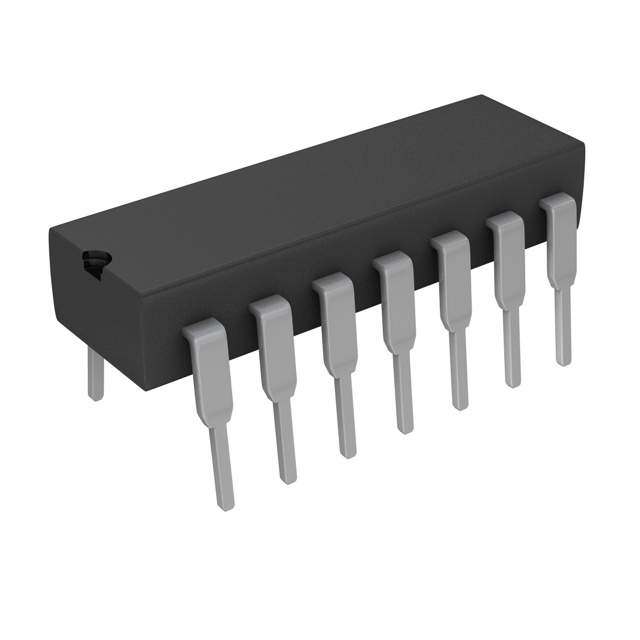
| 描述 | IC REG CTRLR SGL 2V 14-DIP低压差电压控制器 Precision LDO Linear |
| 产品分类 | PMIC - 稳压器 - 线性晶体管驱动器集成电路 - IC |
| 品牌 | Texas Instruments |
| 产品手册 | |
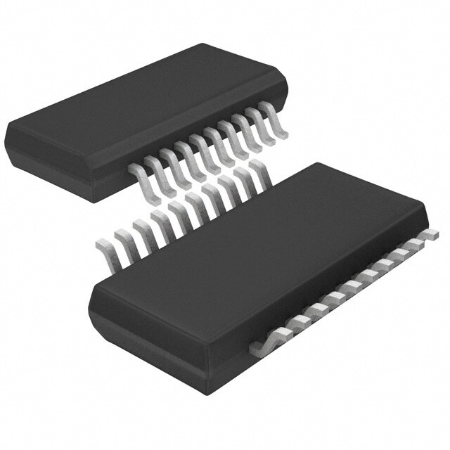
| 产品图片 |
|
| rohs | 符合RoHS无铅 / 符合限制有害物质指令(RoHS)规范要求 |
| 产品系列 | 电源管理 IC,低压差电压控制器,Texas Instruments UC3832N- |
| 数据手册 | |
| 产品型号 | UC3832N |
| 产品目录页面 | |
| 产品种类 | 低压差电压控制器 |
| 供应商器件封装 | 14-PDIP |
| 其它名称 | 296-11273-5 |
| 包装 | 管件 |
| 商标 | Texas Instruments |
| 安装风格 | Through Hole |
| 封装 | Tube |
| 封装/外壳 | 14-DIP(0.300",7.62mm) |
| 封装/箱体 | PDIP-14 |
| 工作温度 | 0°C ~ 70°C |
| 工厂包装数量 | 25 |
| 最大工作温度 | + 70 C |
| 最大输入电压 | 40 V |
| 最小工作温度 | 0 C |
| 最小输入电压 | 4.5 V |
| 标准包装 | 25 |
| 电压-输入 | 4.5 V ~ 36 V |
| 电压-输出 | 2V |
| 电流-电源 | 3.3mA |
| 电源电流 | 3.3 mA |
| 类型 | 正,固定式 |
| 系列 | UC3832 |
| 输出数 | 1 |
| 输出电压 | 2 V |
| 输出电流 | 450 mA |
| 输出类型 | Fixed |


- 商务部:美国ITC正式对集成电路等产品启动337调查
- 曝三星4nm工艺存在良率问题 高通将骁龙8 Gen1或转产台积电
- 太阳诱电将投资9.5亿元在常州建新厂生产MLCC 预计2023年完工
- 英特尔发布欧洲新工厂建设计划 深化IDM 2.0 战略
- 台积电先进制程称霸业界 有大客户加持明年业绩稳了
- 达到5530亿美元!SIA预计今年全球半导体销售额将创下新高
- 英特尔拟将自动驾驶子公司Mobileye上市 估值或超500亿美元
- 三星加码芯片和SET,合并消费电子和移动部门,撤换高东真等 CEO
- 三星电子宣布重大人事变动 还合并消费电子和移动部门
- 海关总署:前11个月进口集成电路产品价值2.52万亿元 增长14.8%


PDF Datasheet 数据手册内容提取
UC1832 UC2832/3 UC3832/3 Precision Low Dropout Linear Controllers FEATURES DESCRIPTION • Precision 1% Reference The UC2832 and UC3833 series of precision linear regulators include all the control functions required in the design of very low dropout linear regulators. • Over-Current Sense Threshold Additionally, they feature an innovative duty-ratio current limiting technique Accurate to 5% which provides peak load capability while limiting the average power dissipa- • Programmable Duty-Ratio tion of the external pass transistor during fault conditions. When the load cur- Over-Current Protection rent reaches an accurately programmed threshold, a gated-astable timer is • 4.5 V to 36 V Operation enabled, which switches the regulator’s pass device off and on at an externally programmable duty-ratio. During the on-time of the pass element, the output • 100mA Output Drive, Source, or current is limited to a value slightly higher than the trip threshold of the duty-ra- Sink tio timer. The constant-current-limit is programmable on the UCx832 to allow • Under-Voltage Lockout higher peak current during the on-time of the pass device. With duty-ratio con- trol, high initial load demands and short circuit protection may both be accom- Additional Features of the UC2832 modated without extra heat sinking or foldback current limiting. Additionally, if series: the timer pin is grounded, the duty-ratio timer is disabled, and the IC operates • Adjustable Current Limit to in constant-voltage/constant-current regulating mode. Current Sense Ratio These IC’s include a 2 Volt (– 1%) reference, error amplifier, UVLO, and a high • Separate +VIN terminal current driver that has both source and sink outputs, allowing the use of either NPN or PNP external pass transistors. Safe operation is assured by the inclu- • Programmable Driver Current sion of under-voltage lockout (UVLO) and thermal shutdown. Limit The UC3833 family includes the basic functions of this design in a low-cost, 8- • Access to VREF and E/A(+) pin mini-dip package, while the UC2832 series provides added versatility with • Logic-Level Disable Input the availability of 14 pins. Packaging options include plastic (N suffix), or ce- ramic (J suffix). Specified operating temperature ranges are: commercial (0°C to 70°C), order UC3832/3 (N or J); and industrial (–40°C to 85°C), order UC2832/3 (N or J). Surface mount packaging is also available. BLOCK DIAGRAMS UDG-92040 SLUS387A - JUNE 1994 - REVISED - MAY 2003
UC1832 UC2832/3 UC3832/3 ABSOLUTE MAXIMUM RATINGS Supply Voltage +VIN. . . . . . . . . . . . . . . . . . . . . . . . . . . . . . . 40V Driver Output Current (Sink or Source) . . . . . . . . . . . . . 450mA Note 1: Unless otherwise indicated, voltages are referenced to ground and currents are positive into, negative out of, the speci- Driver Sink to Source Voltage . . . . . . . . . . . . . . . . . . . . . . . 40V fied terminals. TRC Pin Voltage. . . . . . . . . . . . . . . . . . . . . . . . . . –0.3V to 3.2V Note 2: See Unitrode Integrated Circuits databook for Other Input Voltages. . . . . . . . . . . . . . . . . . . . . . . –0.3V to +VIN information regarding thermal specifications and limitations of Operating Junction Temperature (note 2) . . . –55°C to +150°C packages. Storage Temperature. . . . . . . . . . . . . . . . . . . –65°C to +150°C Lead Temperature (Soldering, 10 Seconds) . . . . . . . . . . 300(cid:176) C CONNECTION DIAGRAMS UC2832 UC3833 DIL-14 (Top View) DIL-8 (Top View) J Or N Package J Or N Package SOIC-16 (Top View) SOIC-16 (Top View) DW Package DW Package LCC-20 & PLCC-20 PACKAGE PIN FUNCTION LCC-20 & PLCC-20 PACKAGE PIN FUNCTION L & Q Package FUNCTION PIN L & Q Package FUNCTION PIN (Top View) N/C 1 (Top View) +VIN & C/S(+) 1 +VIN 2 N/C 2 Comp/Shutdown 3 N/C 3 E/A(+) 4 N/C 4 +2V REF 5 Comp/Shutdown 5 N/C 6 Gnd 6 Gnd 7 N/C 7 Logic Disable 8 N/C 8 Limit 9 N/C 9 Source 10 Source 10 N/C 11 N/C 11 E/A(-) 12 E/A(-) 12 Sink 13 N/C 13 VADJ 14 N/C 14 N/C 15-17 Sink 15 Timer RC 18 Timer RC 16 Current Sense(-) 19 Current Sense(+) 17 Current Sense(+) 20 N/C 18-20 2
UC1832 UC2832/3 UC3832/3 ELECTRICAL CHARACTERISTICS: Unless otherwise stated, specifications hold for TA = 0°C to 70°C for the UC3832/3, –40°C to 85°C for the UC2832/3, +VIN = 15V, Driver sink = +VIN, C/S(+) voltage = +VIN. TA=TJ. PARAMETER TEST CONDITIONS MIN TYP MAX UNITS Input Supply Supply Current +VIN = 6 V 6.5 10 mA +VIN = 36 V 9.5 15 mA Logic Disable = 2 V (UCx832 only) 3.3 mA Reference Section Output Voltage (Note 3) TJ = 25(cid:176) C, IDRIVER = 10 mA 1.98 2.00 2.02 V over temperature, IDRIVER = 10 mA 1.96 2.00 2.04 V Load Regulation (UCx832 only) IO = 0 to 10 m -10 -5.0 mV Line Regulation +VIN = 4.5 V to 36 V, IDRIVER = 10 m 0.033 0.5 mV/V Under-Voltage Lockout Threshold 3.6 4.5 V Logic Disable Input (UCx832 only) Threshold Voltage 1.3 1.4 1.5 V Input Bias Current Logic Disable = 0 V -5.0 -1.0 m A Current Sense Section Comparator Offset 95 100 105 mV Over Temperature 93 100 107 mV Amplifier Offset (UCx833 only) 110 135 170 mV Amplifier Offset (UCx832 only) VADJ = Open 110 135 170 mV VADJ = 1 V 180 235 290 mV VADJ = 0 V 250 305 360 mV Input Bias Current VCM = +VIN 65 100 135 m A Input Offset Current (UCx832 only) VCM = +VIN -10 10 m A Amplifier CMRR (UCx832 only) VCM = 4.1 V to + VIN + 0.3 80 dB Transconductance ICOMP = – 100 m A 65 mS VADJ Input Current (UCx832 only) VADJ = 0V -10 -1 m A Timer Inactive Leakage Current C/S(+) = C/S(-) = +VIN; TRC pin = 2 V 0.25 1.0 m A Active Pullup Current C/S(+) = +VIN, C/S(-) = +VIN - 0.4V; TRC pin = 0 V -345 -270 -175 m A Duty Ratio (note 4) ontime/period, RT = 200k, CT = 0.27m F 4.8 % Period (notes 4,5) ontime + offtime, RT = 200k, CT = 0.27m F 36 ms Upper Trip Threshold (Vu) 1.8 V Lower Trip Threshold (Vl) 0.9 V Trip Threshold Ratio Vu/Vl 2.0 V/V Error Amplifier Input Offset Voltage (UCx832 only) VCM = VCOMP = 2 V -8.0 8.0 mV Input Bias Current VCM = VCOMP = 2 V -4.5 -1.1 m A Input Offset Current (UCx832 only) VCM = VCOMP = 2 V -1.5 1.5 m A AVOL VCOMP = 1 V to 13 V 50 70 dB CMRR (UCx832 only) VCM = 0V to +VIN - 3 V 60 80 dB PSRR (UCx832 only) VCM = 2 V, +VIN = 4.5 V to 36 90 dB Transconductance ICOMP = – 10 m A 4.3 mS VOH ICOMP = 0, Volts below +VIN .95 1.3 V VOL ICOMP = 0 .45 0.7 V IOH VCOMP = 2 V -700 -500 -100 m A 3
UC1832 UC2832/3 UC3832/3 ELECTRICAL CHARACTERISTICS (cont.) Unless otherwise stated, specifications hold for TA = 0°C to 70°C for the UC3832/3, –40°C to 85°C for the UC2832/3, +VIN = 15 V, Driver sink = +VIN, C/S(+) voltage = +VIN. TA=TJ. PARAMETER TEST CONDITIONS MIN TYP MAX UNITS Error Amplifier (cont.) IOL VCOMP = 2 V, C/S(-) = +VIN 100 500 700 m A VCOMP = 2 V, C/S(-) = +VIN - 0.4 V 2 6 mA Driver Maximum Current Driver Limit & Source pins common; TJ = 25°C 200 300 400 mA Over Temperature 100 300 450 mA Limiting Voltage (UCx832 only) Driver Limit to Source voltage at current limit, ISOURCE = -10 mA; TJ = 25°C (Note 6) .72 V Internal Current Sense Resistance TJ = 25°C (Note 6) 2.4 W Pull-Up Current at Driver Sink Compensation/Shutdown = 0.4 V; Driver Sink = +VIN - 1V -800 -300 -100 m A Compensation/Shutdown = 0.4 V, +VIN = 36 V; Driver Sink = 35 V -1000 -300 -75 m A Pull-Down Current at Driver Source Compensation/Shutdown = 0.4 V; Driver Source = 1 V 150 300 700 m A Saturation Voltage Sink to Source Driver Source = 0 V; Driver Current = 100 mA 1.5 V Maximum Source Voltage Driver Sink = +VIN, Driver Current = 100 mA Volts below + VIN 3.0 V UVLO Sink Leakage +VIN = C/S(+) = C/S(-) = 2.5 V, Driver Sink = 15 V, Driver Source = 0 V, TA = 25°C 25 m A Maximum Reverse Source Voltage Compensation/Shutdown = 0 V; ISOURCE = 100 m A, +VIN = 3 V 1.6 V Thermal Shutdown 160 °C Note 3: On the UCx833 this voltage is defined as the regulating level at the error amplifier inverting input, with the error amplifier driving VSOURCE to 2 V. Note 4: These parameters are first-order supply-independent, however both may vary with supply for +VIN less than about 4 V. This supply variation will cause a slight change in the timer period and duty cycle, although a high off-time/on-time ratio will be main- tained. Note 5: With recommended RT value of 200k, TOFF » RT CT * ln(Vu/Vl) – 10%. Note 6: The internal current limiting voltage has a temperature dependence of approximately -2.0 mV/°C, or -2800 ppm/°C. The inter- nal 2.4 W sense resistor has a temperature dependance of approximately +1500 ppm/°C. APPLICATION AND OPERATION INFORMATION NPN Pass (Local 100mA Regulator) (UCx833) UDG-92041-1 4
UC1832 UC2832/3 UC3832/3 APPLICATION AND OPERATION INFORMATION (cont.) PNP Pass (Low Drop-Out Regulator) (UCx833) UDG-92042-1 NPN Pass (Medium Power, Low Drop-Out Regulator) (UCx832) UDG-92043-1 Estimating Maximum Load Capacitance For any power supply, the rate at which the total output Current Sense Amplifier Offset Voltage and K = capacitance can be charged depends on the maximum 100mA output current available and on the nature of the load. For » 1.35 for UCx833, and is variable from 1.35 to 3.05 a constant-current current-limited power supply, the out- with VADJ for the UCx832. put will come up if the load asks for less than the maxi- mum available short-circuit limit current. For a worst-case constant-current load of value just less than ITH, CMAX can be estimated from: To guarantee recovery of a duty-ratio current-limited power supply from a short-circuited load condition, there CMAX = ((K- 1)ITH) (TON), VOUT is a maximum total output capacitance which can be where VOUT is the nominal regulator output voltage. charged for a given unit ON time. The design value of ON time can be adjusted by changing the timing capacitor. For a resistive load of value RL, the value of CMAX can be Nominally, TON = 0.693 x 10k x CT. estimated from: Typically, the IC regulates output current to a maximum of CMAX = TON • 1 . IMAX = K x ITH, where ITH is the timer trip-point current, RL In [(1- K •V ITOHU T• RL) - 1] 5
UC1832 UC2832/3 UC3832/3 APPLICATION AND OPERATION INFORMATION (cont.) Current Sense Amplifier Offset Voltage vs VADJ UCx832/33 Timer Function UCx832/33 Current Sense Input Configuration Load current, timing capacitor voltage, and output voltage of the regulator under fault conditions. 6
UC1832 UC2832/3 UC3832/3 APPLICATION AND OPERATION INFORMATION (cont.) UNITRODE CORPORATION 7 CONTINENTAL BLVD. • MERRIMACK, NH 03054 TEL. (603) 424-2410 • FAX (603) 424-3460 7
PACKAGE OPTION ADDENDUM www.ti.com 12-May-2015 PACKAGING INFORMATION Orderable Device Status Package Type Package Pins Package Eco Plan Lead/Ball Finish MSL Peak Temp Op Temp (°C) Device Marking Samples (1) Drawing Qty (2) (6) (3) (4/5) 5962-9326501M2A ACTIVE LCCC FK 20 1 TBD POST-PLATE N / A for Pkg Type -55 to 125 5962- 9326501M2A UC1832L/ 883B 5962-9326501MCA ACTIVE CDIP J 14 1 TBD A42 N / A for Pkg Type -55 to 125 5962-9326501MC A UC1832J/883B 5962-9326501V2A ACTIVE LCCC FK 20 1 TBD POST-PLATE N / A for Pkg Type 5962- 9326501V2A UC1832L QMLV 5962-9326501VCA ACTIVE CDIP J 14 1 TBD A42 N / A for Pkg Type 5962-9326501VC A UC1832JQMLV UC1832J ACTIVE CDIP J 14 1 TBD A42 N / A for Pkg Type -55 to 125 UC1832J UC1832J883B ACTIVE CDIP J 14 1 TBD A42 N / A for Pkg Type -55 to 125 5962-9326501MC A UC1832J/883B UC1832L883B ACTIVE LCCC FK 20 1 TBD POST-PLATE N / A for Pkg Type -55 to 125 5962- 9326501M2A UC1832L/ 883B UC2832DW ACTIVE SOIC DW 16 40 Green (RoHS CU NIPDAU Level-2-260C-1 YEAR -25 to 85 UC2832DW & no Sb/Br) UC2832DWTR ACTIVE SOIC DW 16 2000 Green (RoHS CU NIPDAU Level-2-260C-1 YEAR -25 to 85 UC2832DW & no Sb/Br) UC2833DW ACTIVE SOIC DW 16 40 Green (RoHS CU NIPDAU Level-2-260C-1 YEAR -40 to 85 UC2833DW & no Sb/Br) UC2833DWG4 ACTIVE SOIC DW 16 40 Green (RoHS CU NIPDAU Level-2-260C-1 YEAR -40 to 85 UC2833DW & no Sb/Br) UC2833DWTR ACTIVE SOIC DW 16 2000 Green (RoHS CU NIPDAU Level-2-260C-1 YEAR -40 to 85 UC2833DW & no Sb/Br) UC2833J OBSOLETE CDIP JG 8 TBD Call TI Call TI -40 to 85 UC2833N LIFEBUY PDIP P 8 50 Green (RoHS CU NIPDAU N / A for Pkg Type -40 to 85 UC2833N & no Sb/Br) Addendum-Page 1
PACKAGE OPTION ADDENDUM www.ti.com 12-May-2015 Orderable Device Status Package Type Package Pins Package Eco Plan Lead/Ball Finish MSL Peak Temp Op Temp (°C) Device Marking Samples (1) Drawing Qty (2) (6) (3) (4/5) UC3832DW ACTIVE SOIC DW 16 40 Green (RoHS CU NIPDAU Level-2-260C-1 YEAR 0 to 70 UC3832DW & no Sb/Br) UC3832DWG4 ACTIVE SOIC DW 16 40 Green (RoHS CU NIPDAU Level-2-260C-1 YEAR 0 to 70 UC3832DW & no Sb/Br) UC3832N LIFEBUY PDIP N 14 25 Green (RoHS CU NIPDAU N / A for Pkg Type 0 to 70 UC3832N & no Sb/Br) UC3832NG4 LIFEBUY PDIP N 14 25 Green (RoHS CU NIPDAU N / A for Pkg Type 0 to 70 UC3832N & no Sb/Br) UC3833DW ACTIVE SOIC DW 16 40 Green (RoHS CU NIPDAU Level-2-260C-1 YEAR 0 to 70 UC3833DW & no Sb/Br) UC3833DWTR ACTIVE SOIC DW 16 2000 Green (RoHS CU NIPDAU Level-2-260C-1 YEAR 0 to 70 UC3833DW & no Sb/Br) UC3833J OBSOLETE CDIP JG 8 TBD Call TI Call TI 0 to 70 UC3833N LIFEBUY PDIP P 8 50 Green (RoHS CU NIPDAU N / A for Pkg Type 0 to 70 UC3833N & no Sb/Br) UC3833NG4 LIFEBUY PDIP P 8 50 Green (RoHS CU NIPDAU N / A for Pkg Type 0 to 70 UC3833N & no Sb/Br) (1) The marketing status values are defined as follows: ACTIVE: Product device recommended for new designs. LIFEBUY: TI has announced that the device will be discontinued, and a lifetime-buy period is in effect. NRND: Not recommended for new designs. Device is in production to support existing customers, but TI does not recommend using this part in a new design. PREVIEW: Device has been announced but is not in production. Samples may or may not be available. OBSOLETE: TI has discontinued the production of the device. (2) Eco Plan - The planned eco-friendly classification: Pb-Free (RoHS), Pb-Free (RoHS Exempt), or Green (RoHS & no Sb/Br) - please check http://www.ti.com/productcontent for the latest availability information and additional product content details. TBD: The Pb-Free/Green conversion plan has not been defined. Pb-Free (RoHS): TI's terms "Lead-Free" or "Pb-Free" mean semiconductor products that are compatible with the current RoHS requirements for all 6 substances, including the requirement that lead not exceed 0.1% by weight in homogeneous materials. Where designed to be soldered at high temperatures, TI Pb-Free products are suitable for use in specified lead-free processes. Pb-Free (RoHS Exempt): This component has a RoHS exemption for either 1) lead-based flip-chip solder bumps used between the die and package, or 2) lead-based die adhesive used between the die and leadframe. The component is otherwise considered Pb-Free (RoHS compatible) as defined above. Green (RoHS & no Sb/Br): TI defines "Green" to mean Pb-Free (RoHS compatible), and free of Bromine (Br) and Antimony (Sb) based flame retardants (Br or Sb do not exceed 0.1% by weight in homogeneous material) (3) MSL, Peak Temp. - The Moisture Sensitivity Level rating according to the JEDEC industry standard classifications, and peak solder temperature. (4) There may be additional marking, which relates to the logo, the lot trace code information, or the environmental category on the device. Addendum-Page 2
PACKAGE OPTION ADDENDUM www.ti.com 12-May-2015 (5) Multiple Device Markings will be inside parentheses. Only one Device Marking contained in parentheses and separated by a "~" will appear on a device. If a line is indented then it is a continuation of the previous line and the two combined represent the entire Device Marking for that device. (6) Lead/Ball Finish - Orderable Devices may have multiple material finish options. Finish options are separated by a vertical ruled line. Lead/Ball Finish values may wrap to two lines if the finish value exceeds the maximum column width. Important Information and Disclaimer:The information provided on this page represents TI's knowledge and belief as of the date that it is provided. TI bases its knowledge and belief on information provided by third parties, and makes no representation or warranty as to the accuracy of such information. Efforts are underway to better integrate information from third parties. TI has taken and continues to take reasonable steps to provide representative and accurate information but may not have conducted destructive testing or chemical analysis on incoming materials and chemicals. TI and TI suppliers consider certain information to be proprietary, and thus CAS numbers and other limited information may not be available for release. In no event shall TI's liability arising out of such information exceed the total purchase price of the TI part(s) at issue in this document sold by TI to Customer on an annual basis. OTHER QUALIFIED VERSIONS OF UC1832, UC1832-SP, UC2832, UC3832, UC3833 : •Catalog: UC3832, UC1832 •Enhanced Product: UC2832-EP •Military: UC1832, UC1833 •Space: UC1832-SP NOTE: Qualified Version Definitions: •Catalog - TI's standard catalog product •Enhanced Product - Supports Defense, Aerospace and Medical Applications •Military - QML certified for Military and Defense Applications •Space - Radiation tolerant, ceramic packaging and qualified for use in Space-based application Addendum-Page 3
PACKAGE MATERIALS INFORMATION www.ti.com 18-Aug-2014 TAPE AND REEL INFORMATION *Alldimensionsarenominal Device Package Package Pins SPQ Reel Reel A0 B0 K0 P1 W Pin1 Type Drawing Diameter Width (mm) (mm) (mm) (mm) (mm) Quadrant (mm) W1(mm) UC2832DWTR SOIC DW 16 2000 330.0 16.4 10.75 10.7 2.7 12.0 16.0 Q1 UC2833DWTR SOIC DW 16 2000 330.0 16.4 10.75 10.7 2.7 12.0 16.0 Q1 UC3833DWTR SOIC DW 16 2000 330.0 16.4 10.75 10.7 2.7 12.0 16.0 Q1 PackMaterials-Page1
PACKAGE MATERIALS INFORMATION www.ti.com 18-Aug-2014 *Alldimensionsarenominal Device PackageType PackageDrawing Pins SPQ Length(mm) Width(mm) Height(mm) UC2832DWTR SOIC DW 16 2000 367.0 367.0 38.0 UC2833DWTR SOIC DW 16 2000 367.0 367.0 38.0 UC3833DWTR SOIC DW 16 2000 367.0 367.0 38.0 PackMaterials-Page2
MECHANICAL DATA MCER001A – JANUARY 1995 – REVISED JANUARY 1997 JG (R-GDIP-T8) CERAMIC DUAL-IN-LINE 0.400 (10,16) 0.355 (9,00) 8 5 0.280 (7,11) 0.245 (6,22) 1 4 0.065 (1,65) 0.045 (1,14) 0.063 (1,60) 0.020 (0,51) MIN 0.310 (7,87) 0.015 (0,38) 0.290 (7,37) 0.200 (5,08) MAX Seating Plane 0.130 (3,30) MIN 0.023 (0,58) 0°–15° 0.015 (0,38) 0.100 (2,54) 0.014 (0,36) 0.008 (0,20) 4040107/C 08/96 NOTES: A. All linear dimensions are in inches (millimeters). B. This drawing is subject to change without notice. C. This package can be hermetically sealed with a ceramic lid using glass frit. D. Index point is provided on cap for terminal identification. E. Falls within MIL STD 1835 GDIP1-T8 • POST OFFICE BOX 655303 DALLAS, TEXAS 75265
None
None
None
None
None
None
IMPORTANTNOTICE TexasInstrumentsIncorporatedanditssubsidiaries(TI)reservetherighttomakecorrections,enhancements,improvementsandother changestoitssemiconductorproductsandservicesperJESD46,latestissue,andtodiscontinueanyproductorserviceperJESD48,latest issue.Buyersshouldobtainthelatestrelevantinformationbeforeplacingordersandshouldverifythatsuchinformationiscurrentand complete.Allsemiconductorproducts(alsoreferredtohereinas“components”)aresoldsubjecttoTI’stermsandconditionsofsale suppliedatthetimeoforderacknowledgment. TIwarrantsperformanceofitscomponentstothespecificationsapplicableatthetimeofsale,inaccordancewiththewarrantyinTI’sterms andconditionsofsaleofsemiconductorproducts.TestingandotherqualitycontroltechniquesareusedtotheextentTIdeemsnecessary tosupportthiswarranty.Exceptwheremandatedbyapplicablelaw,testingofallparametersofeachcomponentisnotnecessarily performed. TIassumesnoliabilityforapplicationsassistanceorthedesignofBuyers’products.Buyersareresponsiblefortheirproductsand applicationsusingTIcomponents.TominimizetherisksassociatedwithBuyers’productsandapplications,Buyersshouldprovide adequatedesignandoperatingsafeguards. TIdoesnotwarrantorrepresentthatanylicense,eitherexpressorimplied,isgrantedunderanypatentright,copyright,maskworkright,or otherintellectualpropertyrightrelatingtoanycombination,machine,orprocessinwhichTIcomponentsorservicesareused.Information publishedbyTIregardingthird-partyproductsorservicesdoesnotconstitutealicensetousesuchproductsorservicesorawarrantyor endorsementthereof.Useofsuchinformationmayrequirealicensefromathirdpartyunderthepatentsorotherintellectualpropertyofthe thirdparty,oralicensefromTIunderthepatentsorotherintellectualpropertyofTI. ReproductionofsignificantportionsofTIinformationinTIdatabooksordatasheetsispermissibleonlyifreproductioniswithoutalteration andisaccompaniedbyallassociatedwarranties,conditions,limitations,andnotices.TIisnotresponsibleorliableforsuchaltered documentation.Informationofthirdpartiesmaybesubjecttoadditionalrestrictions. ResaleofTIcomponentsorserviceswithstatementsdifferentfromorbeyondtheparametersstatedbyTIforthatcomponentorservice voidsallexpressandanyimpliedwarrantiesfortheassociatedTIcomponentorserviceandisanunfairanddeceptivebusinesspractice. TIisnotresponsibleorliableforanysuchstatements. Buyeracknowledgesandagreesthatitissolelyresponsibleforcompliancewithalllegal,regulatoryandsafety-relatedrequirements concerningitsproducts,andanyuseofTIcomponentsinitsapplications,notwithstandinganyapplications-relatedinformationorsupport thatmaybeprovidedbyTI.Buyerrepresentsandagreesthatithasallthenecessaryexpertisetocreateandimplementsafeguardswhich anticipatedangerousconsequencesoffailures,monitorfailuresandtheirconsequences,lessenthelikelihoodoffailuresthatmightcause harmandtakeappropriateremedialactions.BuyerwillfullyindemnifyTIanditsrepresentativesagainstanydamagesarisingoutoftheuse ofanyTIcomponentsinsafety-criticalapplications. Insomecases,TIcomponentsmaybepromotedspecificallytofacilitatesafety-relatedapplications.Withsuchcomponents,TI’sgoalisto helpenablecustomerstodesignandcreatetheirownend-productsolutionsthatmeetapplicablefunctionalsafetystandardsand requirements.Nonetheless,suchcomponentsaresubjecttotheseterms. NoTIcomponentsareauthorizedforuseinFDAClassIII(orsimilarlife-criticalmedicalequipment)unlessauthorizedofficersoftheparties haveexecutedaspecialagreementspecificallygoverningsuchuse. OnlythoseTIcomponentswhichTIhasspecificallydesignatedasmilitarygradeor“enhancedplastic”aredesignedandintendedforusein military/aerospaceapplicationsorenvironments.BuyeracknowledgesandagreesthatanymilitaryoraerospaceuseofTIcomponents whichhavenotbeensodesignatedissolelyattheBuyer'srisk,andthatBuyerissolelyresponsibleforcompliancewithalllegaland regulatoryrequirementsinconnectionwithsuchuse. TIhasspecificallydesignatedcertaincomponentsasmeetingISO/TS16949requirements,mainlyforautomotiveuse.Inanycaseofuseof non-designatedproducts,TIwillnotberesponsibleforanyfailuretomeetISO/TS16949. Products Applications Audio www.ti.com/audio AutomotiveandTransportation www.ti.com/automotive Amplifiers amplifier.ti.com CommunicationsandTelecom www.ti.com/communications DataConverters dataconverter.ti.com ComputersandPeripherals www.ti.com/computers DLP®Products www.dlp.com ConsumerElectronics www.ti.com/consumer-apps DSP dsp.ti.com EnergyandLighting www.ti.com/energy ClocksandTimers www.ti.com/clocks Industrial www.ti.com/industrial Interface interface.ti.com Medical www.ti.com/medical Logic logic.ti.com Security www.ti.com/security PowerMgmt power.ti.com Space,AvionicsandDefense www.ti.com/space-avionics-defense Microcontrollers microcontroller.ti.com VideoandImaging www.ti.com/video RFID www.ti-rfid.com OMAPApplicationsProcessors www.ti.com/omap TIE2ECommunity e2e.ti.com WirelessConnectivity www.ti.com/wirelessconnectivity MailingAddress:TexasInstruments,PostOfficeBox655303,Dallas,Texas75265 Copyright©2015,TexasInstrumentsIncorporated