ICGOO在线商城 > UC2914N
 Datasheet下载
- 型号: UC2914N
- 制造商: Texas Instruments
- 库位|库存: xxxx|xxxx
- 要求:
| 数量阶梯 | 香港交货 | 国内含税 |
| +xxxx | $xxxx | ¥xxxx |
查看当月历史价格
查看今年历史价格
UC2914N产品简介:
ICGOO电子元器件商城为您提供UC2914N由Texas Instruments设计生产,在icgoo商城现货销售,并且可以通过原厂、代理商等渠道进行代购。 提供UC2914N价格参考以及Texas InstrumentsUC2914N封装/规格参数等产品信息。 你可以下载UC2914N参考资料、Datasheet数据手册功能说明书, 资料中有UC2914N详细功能的应用电路图电压和使用方法及教程。
| 参数 | 数值 |
| 产品目录 | 集成电路 (IC)半导体 |
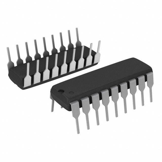
| 描述 | IC 5V TO 35V PWR MANAGER 18-DIP热交换电压控制器 5-35V Single Industral Temp. |
| 产品分类 | |
| 品牌 | Texas Instruments |
| 产品手册 | |
| 产品图片 |
|
| rohs | 符合RoHS无铅 / 符合限制有害物质指令(RoHS)规范要求 |
| 产品系列 | 电源管理 IC,热交换电压控制器,Texas Instruments UC2914N- |
| 数据手册 | |
| 产品型号 | UC2914N |
| 产品 | Controllers & Switches |
| 产品目录页面 | |
| 产品种类 | 热交换电压控制器 |
| 供应商器件封装 | 18-PDIP |
| 其它名称 | 296-2502-5 |
| 内部开关 | 无 |
| 功能引脚 | CT, /FAULT, IMAX, LR, OSC, OSCB, PLIM, PMP, PMPB, REF, /SD, VPUMP |
| 包装 | 管件 |
| 单位重量 | 1.206 g |
| 可编程特性 | 自动重试,断路器,限流,故障超时,闭锁故障 |
| 商标 | Texas Instruments |
| 安装类型 | 通孔 |
| 安装风格 | Through Hole |
| 封装 | Tube |
| 封装/外壳 | 18-DIP(0.300",7.62mm) |
| 封装/箱体 | PDIP-18 |
| 工作温度 | -40°C ~ 85°C |
| 工作温度范围 | - 40 C to + 85 C |
| 工厂包装数量 | 20 |
| 应用 | 通用 |
| 标准包装 | 20 |
| 特性 | UVLO |
| 电压-电源 | 5 V ~ 35 V |
| 电流-电源 | 12mA |
| 电流-输出(最大值) | - |
| 电源电压-最大 | 35 V |
| 电源电压-最小 | 5 V |
| 电源电流 | 20 mA |
| 类型 | 热交换控制器 |
| 系列 | UC2914 |
| 通道数 | 1 |
| 通道数量 | 1 Channel |


- 商务部:美国ITC正式对集成电路等产品启动337调查
- 曝三星4nm工艺存在良率问题 高通将骁龙8 Gen1或转产台积电
- 太阳诱电将投资9.5亿元在常州建新厂生产MLCC 预计2023年完工
- 英特尔发布欧洲新工厂建设计划 深化IDM 2.0 战略
- 台积电先进制程称霸业界 有大客户加持明年业绩稳了
- 达到5530亿美元!SIA预计今年全球半导体销售额将创下新高
- 英特尔拟将自动驾驶子公司Mobileye上市 估值或超500亿美元
- 三星加码芯片和SET,合并消费电子和移动部门,撤换高东真等 CEO
- 三星电子宣布重大人事变动 还合并消费电子和移动部门
- 海关总署:前11个月进口集成电路产品价值2.52万亿元 增长14.8%


PDF Datasheet 数据手册内容提取
(cid:1)(cid:2)(cid:3)(cid:4)(cid:5)(cid:6) (cid:1)(cid:2)(cid:7)(cid:4)(cid:5)(cid:6) (cid:8) SLUS425C − DECEMBER 2003 − REVISED JULY 2004 (cid:9)(cid:10)(cid:11) (cid:12)(cid:13) (cid:7)(cid:9)(cid:10)(cid:11) (cid:14)(cid:15)(cid:16) (cid:17)(cid:18)(cid:19)(cid:20) (cid:20)(cid:15)(cid:18)(cid:21)(cid:22) (cid:23)(cid:19)(cid:24)(cid:19)(cid:25)(cid:21)(cid:22) FEATURES DESCRIPTION (cid:1) 5-V to 35-V Operation The UC3914 family of hot swap power managers (cid:1) Precision Maximum Current Control provides complete power management, hot swap (cid:1) Precision Fault Threshold and fault handling capability. Integrating this part (cid:1) and a few external components, allows a board to Programmable Average Power Limiting be swapped in or out upon failure or system (cid:1) Programmable Overcurrent Limit modification without removing power to the (cid:1) Shutdown Control hardware, while maintaining the integrity of the (cid:1) Charge Pump for Low R High-Side powered system. Complementary output drivers DS(on) Drive and diodes have been integrated for use with (cid:1) external capacitors as a charge pump to ensure W Latch Reset Function Available sufficient gate drive to the external N-channel (cid:1) Output Drive V Clamping E GS MOSFET transistor for low R . All control and DS(on) (cid:1) I Fault Output Indication housekeeping functions are integrated and V (cid:1) 18-Pin DIL and SOIC Packages externally programmable and include the fault E current level, maximum output sourcing current, R maximum fault time and average power limiting of P SIMPLIFIED APPLICATION DIAGRAM the external FET. The UC3914 features a duty T ratio current limiting technique, which provides C peak load capability while limiting the average U power dissipation of the external pass transistor D during fault conditions. The fault level is fixed at 6 9 18 16 VCC 50 mV with respect to VCC to minimize total O OSC PMP REF IMAX dropout. R P 1 PMPB VCC 2 The fault current level is set with an external current sense resistor. The maximum allowable UC2914/UC3914 sourcing current is programmed by using a resistor divider from VCC to REF to set the voltage 5 OSCB SENSE 17 on IMAX. The maximum current level, when the output appears as a current source is (VVCC − 7 VPUMP V )/R . OUT 11 IMAX SENSE This part is offered in both 18-pin DW wide-body 4 SD VOUTS 12 (SOIC) and dual-in-line (DIL) packages. VOUT 10 FAULT PLIM 14 GND LR CT 1 13 15 VOUT VCC UDG−03114 Please be aware that an important notice concerning availability, standard warranty, and use in critical applications of TexasInstruments semiconductor products and disclaimers thereto appears at the end of this data sheet. (cid:20)(cid:22)(cid:15)(cid:26)(cid:1)(cid:2)(cid:16) (cid:20)(cid:22)(cid:21)(cid:11)(cid:27)(cid:21)(cid:18) (cid:28)(cid:29)(cid:30)(cid:13)(cid:31)!"(cid:12)(cid:28)(cid:13)(cid:29) #(cid:13)(cid:29)#$(cid:31)(cid:29)% &(cid:31)(cid:13)’(#(cid:12)% (cid:28)(cid:29) (cid:12))$ (cid:30)(cid:13)(cid:31)!"(cid:12)(cid:28)*$ (cid:13)(cid:31) Copyright 2003, Texas Instruments Incorporated ’$%(cid:28)+(cid:29) &)"%$ (cid:13)(cid:30) ’$*$,(cid:13)&!$(cid:29)(cid:12)- (cid:2))"(cid:31)"#(cid:12)$(cid:31)(cid:28)%(cid:12)(cid:28)# ’"(cid:12)" "(cid:29)’ (cid:13)(cid:12))$(cid:31) %&$#(cid:28)(cid:30)(cid:28)#"(cid:12)(cid:28)(cid:13)(cid:29)% "(cid:31)$ ’$%(cid:28)+(cid:29) +(cid:13)",%- (cid:16)$."% (cid:27)(cid:29)%(cid:12)(cid:31)(!$(cid:29)(cid:12)% (cid:31)$%$(cid:31)*$% (cid:12))$ (cid:31)(cid:28)+)(cid:12) (cid:12)(cid:13) #)"(cid:29)+$ (cid:13)(cid:31) ’(cid:28)%#(cid:13)(cid:29)(cid:12)(cid:28)(cid:29)($ (cid:12))$%$ &(cid:31)(cid:13)’(#(cid:12)% /(cid:28)(cid:12))(cid:13)((cid:12) (cid:29)(cid:13)(cid:12)(cid:28)#$- www.ti.com 1
(cid:1)(cid:2)(cid:3)(cid:4)(cid:5)(cid:6) (cid:1)(cid:2)(cid:7)(cid:4)(cid:5)(cid:6) (cid:8) SLUS425C − DECEMBER 2003 − REVISED JULY 2004 DESCRIPTION (continued) When the output current is less than the fault level, the external output transistor remains switched on. When the output current exceeds the fault level, but is less than the maximum sourcing level programmed by IMAX, the output remains switched on, and the fault timer starts to charge C , a timing capacitor. Once C charges T T to 2.5 V, the output device is turned off and C is slowly discharged. Once C is discharged to 0.5 V, the device T T performs a retry and the output transistor is switched on again. The UC3914 offers two distinct reset modes. In one mode with LR left floating or held low, the device tries to reset itself repeatedly if a fault occurs as described above. In the second mode with LR held high, once a fault occurs, the output is latched off until either LR is toggled low, the part is shutdown then re−enabled using SD, or the power to the part is turned off and then on again. ABSOLUTE MAXIMUM RATINGS over operating free-air temperature range unless otherwise noted.(1)(2) UC2914 UNIT UC3914 Input supply voltage VCC 40 SD, LR 12 VV MMaaxxiimmuumm ffoorrcceedd vvoollttaaggee IMAX VCC W FAULT 20 MMaaxxiimmuumm ccuurrrreenntt mmAA PLIM 10 E I Maximum voltage FAULT 40 V V Reference output current internally limited A E R Storage temperature range, Tstg −65 to 150 P Junction temperature range, TJ −55 to 150 °CC Lead temperature 1,6 mm (1/16 inch) from case for 10 seconds 300 T (1)Stresses beyond those listed under absolute maximum ratings may cause permanent damage to the device. These are stress ratings only, C and functional operation of the device at these or any other conditions beyond those indicated under recommended operating conditions is U not implied. Exposure to Absolute Maximum Rated conditions for extended periods may affect device reliability D (2)Currents are positive into and negative out of the specifief terminal unless otherwise noted. All voltage values are with respect to the network ground terminal. O R RECOMMENDED OPERATING CONDITIONS P MIN NOM MAX UNIT Supply voltage, VCC 5 35 V UC2914 −40 85 OOppeerraattiinngg ffrreeee--aaiirr tteemmppeerraattuurree rraannggee,, TTAA °°CC UC3914 0 70 2 www.ti.com
(cid:1)(cid:2)(cid:3)(cid:4)(cid:5)(cid:6) (cid:1)(cid:2)(cid:7)(cid:4)(cid:5)(cid:6) (cid:8) SLUS425C − DECEMBER 2003 − REVISED JULY 2004 ELECTRICAL CHARACTERISTICS TA = 0°C to 70°C for the UC3914, −40°C to 85°C for the UC2914, VCC = 12V, VPUMP = VPUMP(max), SD = 5 V, CP1 = CP2 = CPUMP= 0.01 µF. TA = TJ. (Unless otherwise specified) PARAMETER TEST CONDITIONS MIN TYP MAX UNIT SUPPLY CURRENTS 8 15 IICCCC SSuuppppllyy ccuurrrreenntt((22)) mmAA VCC = 35 V 12 20 ICCSD Shutdown supply current SD = 0 V, 500 900 µA UVLO turn−on threshold voltage 4.0 4.4 V UVLO hysteresis 55 120 250 mV FAULT TIMING TJ = 25°C, wrt VCC −55 −50 −45 OOvveerrccuurrrreenntt tthhrreesshhoolldd mmVV Over operating temperature wrt VCC −57 −50 −42 IMAX input bias 1 3 µAA VCT = 1 V −140 −100 −60 IICCTT__CCHHGG CCTT cchhaarrggee ccuurrrreenntt VCT = 1 V, overload condition −6.0 −3.0 −1.5 mA ICT_DSCH CT discharge current VCT = 1 V 2.0 3.0 4.5 µA VCT_FLT CT fault threshold voltage 2.25 2.50 2.75 W VV VCT_RST CT reset threshold voltage 0.45 0.50 0.55 E Output duty cycle Fault condition, IPL = 0 A 1.5% 3.0% 4.5% I V OUTPUT E VVOUTS = VCC, VPUMP = VPUMP(max), R −1.5 −1.0 wrt VPUMP P VVOOHH HHiigghh--lleevveell oouuttppuutt vvoollttaaggee VVOUTS = VCC, VPUMP = VPUMP(max), −2.0 −1.5 IOUT = −2 mA, wrt VPUMP T C IOUT = 0 A 0.8 1.3 VV U IOUT = 5 mA 1 2 VVOOLL LLooww--lleevveell oouuttppuutt vvoollttaaggee D IOUT = 25 mA, VVOUTS = 0 V overload condition 1.2 1.8 O VOUT(cl) Output clamp voltage VOUTS = 0 V 11.5 13.0 14.5 R tRISE Rise time(1) COUT = 1 nF 750 1250 P nnss tFALL Fall time(1) COUT = 1 nF 250 500 LINEAR CURRENT AMPLIFIER VIO Input offset voltage −15 0 15 mV Voltage gain 60 80 dB VIMAX = VOUT, VSENSE = VVCC, wrt VCC −20 0 20 VVIIMMAAXX IIMMAAXX ccoonnttrrooll vvoollttaaggee mmVV VIMAX = VOUT, VSENSE = VREF, wrt REF −20 0 20 SENSE input bias 1.5 3.5 µA SHUTDOWN Shutdown threshold voltage 0.6 1.5 2.0 V input current SD = 5 V 150 300 µA Delay to output time(1) 0.5 2.0 µs (1)Ensured by design. Not production tested. (2)A mathematical averaging is used to determine this value. See Application Section for more information. www.ti.com 3
(cid:1)(cid:2)(cid:3)(cid:4)(cid:5)(cid:6) (cid:1)(cid:2)(cid:7)(cid:4)(cid:5)(cid:6) (cid:8) SLUS425C − DECEMBER 2003 − REVISED JULY 2004 ELECTRICAL CHARACTERISTICS TA = 0°C to 70°C for the UC3914, −40°C to 85°C for the UC2914, VCC = 12V, VPUMP = VPUMP(max), SD = 5 V, CP1 = CP2 = CPUMP= 0.01 µF. TA = TJ. (Unless otherwise specified) PARAMETER TEST CONDITIONS MIN TYP MAX UNIT CHARGE PUMP fOSC, Oscillator frequency OSC, OSCB 60 150 250 kHz fOSCB VOH High-level output voltage IOSC = −5 mA 10.0 11.0 11.6 VV VOL Low-level output voltage IOSC = 5 mA 0.2 0.5 Output clamp voltage VCC = 25 V 18.5 20.5 22.5 V ILIM Output current limit High side only −20 −10 −3 mA IDIODE = 10 mA, measured from PMP to Pump diode voltage drop 0.5 0.9 1.3 PMPB, PMPB to VPUMP PMP clamp voltage VCC = 25 V 18.5 20.5 22.5 VVOUTS = VCC charge pump disable threshold, 20 22 24 VCC = 12 V VVPPUUMMPP mmaaxxiimmuumm vvoollttaaggee VVOUTS = VCC charge pump disable threshold, V 42 45 48 VCC = 35 V W VVOUTS = VCC charge pump re-enable 0.3 0.7 1.4 threshold, VCC = 12 V E VVPPUUMMPP hhyysstteerreessiiss I VVOUTS = VCC charge pump re-enable 0.25 0.70 1.40 V threshold, VCC = 35 V E REFERENCE R REF output voltage wrt VCC −2.25 −2.00 −1.75 V P REF current limit 12.5 20.0 50.0 mA T Load regulation 1 mA ≤ IVREF ≤ 5 mA 25 60 C Line regulation 5 V ≤ VVCC ≤ 35 V 25 100 mmVV U FAULT D Low-level output voltage IFAULT = 1 mA 100 200 mV O Output leakage VFAULT = 35 V 10 500 nA R LATCH P Latch release threshold voltage High-to-low 0.6 1.4 2.0 V Input current VLR = 5 V 500 750 µA POWER LIMITING IPLIM = 200 µA In fault mode 0.6% 1.3% 2.0% DDuuttyy ccyyccllee ccoonnttrrooll IPLIM = 3 mA In fault mode 0.05% 0.12% 0.20% OVERLOAD Delay-to-output time(1) 500 1250 ns Threshold voltage wrt IMAX −250 −200 −150 mV (1)Ensured by design. Not production tested. (2)A mathematical averaging is used to determine this value. See Application Section for more information. 4 www.ti.com
(cid:1)(cid:2)(cid:3)(cid:4)(cid:5)(cid:6) (cid:1)(cid:2)(cid:7)(cid:4)(cid:5)(cid:6) (cid:8) SLUS425C − DECEMBER 2003 − REVISED JULY 2004 AVAILABLE OPTIONS PACKAGED DEVICES TA PLASTIC DIL−18 PLASTIC SOIC (N) (DW)(1) −40°C to 85°C UC2914N UC2914DW 0°C to 70°C UC3914N UC3914DW (1)The DW package is available taped and reeled. Add an TR suffix to the device type (e.g. UC2914DWTR) to order quantities of 2,000 devices per reel. DIL−18 SOIC−18 N PACKAGE DW PACKAGE (TOP VIEW) (TOP VIEW) GND 1 18 REF GND 1 18 REF VCC 2 17 SENSE VCC 2 17 SENSE N/C 3 16 IMAX N/C 3 16 IMAX SD 4 15 CT SD 4 15 CT OSCB 5 14 PLIM OSCB 5 14 PLIM OSC 6 13 LR OSC 6 13 LR W VPUMP 7 12 VOUTS VPUMP 7 12 VOUTS PMPB 8 11 OUT E PMPB 8 11 OUT PMP 9 10 FAULT I PMP 9 10 FAULT V E R BLOCK DIAGRAM P T C U D O R P UDG−95134−2 www.ti.com 5
(cid:1)(cid:2)(cid:3)(cid:4)(cid:5)(cid:6) (cid:1)(cid:2)(cid:7)(cid:4)(cid:5)(cid:6) (cid:8) SLUS425C − DECEMBER 2003 − REVISED JULY 2004 TERMINAL FUNCTIONS TERMINAL II//OO DDEESSCCRRIIPPTTIIOONN NAME NO. A capacitor is connected to this pin in order to set the maximum fault time. The minimum fault time must be more than the time to charge external load capacitance. The fault time is defined as shown in equation (1) CT 15 I/O where ICH = 100 µA + IPL, where IPL is the current into the power limit pin. Once the fault time is reached the output shuts down for a time given by equation (2) where IDIS is nominally 3 µA.. Open collector output which pulls low upon any of the following conditions: timer fault, shutdown, UVLO. This FAULT 10 O pin MUST be pulled up to VVCC or another supply through a suitable impedance. GND 1 − Ground reference for the device. This pin programs the maximum allowable sourcing current. Since REF is a −2-V reference (with respect to VCC), a voltage divider can be derived from VCC to REF in order to generate the program level for the IMAX IMAX 16 I pin. The current level at which the output appears as a current source is equal to the voltage on the IMAX pin, with respect to VCC, divided by the current sense resistor. If desired, a controlled current startup can be pro- grammed with a capacitor on IMAX to VCC. If this pin is held high and a fault occurs, the timer is prevented from resetting the fault latch when CT is dis- charged below the reset comparator threshold. The part does not retry until this pin is brought to a logic low or a LR 13 I power-on-reset occurs. Pulling this pin low before the reset time is reached does not clear the fault until the reset time is reached. Floating or holding this pin low results in the part repeatedly trying to reset itself if a fault occurs. W OUT 11 O Output drive to the MOSFET pass element. Internal clamping ensures that the maximum VGS drive is 15 V. E OSC 6 O CCoommpplleemmeennttaarryy oouuttppuutt ddrriivveerrss ffoorr iinntteerrmmeeddiiaattee cchhaarrggee ppuummpp ssttaaggeess.. AA 00..0011--µµFF ccaappaacciittoorr sshhoouulldd bbee ppllaacceedd I OSCB 5 O between OSC and PMP, and OSCB and PMPB. V This feature ensures that the average MOSFET power dissipation is controlled. A resistor is connected from this E PLIM 14 I pin to VCC. Current flows into PLIM, adding to the fault timer charge current, reducing the duty cycle from the R typical 3% level. When IPL >> 100 µA then the average MOSFET power dissipation is given by equation (3). P PMP 9 I CCoommpplleemmeennttaarryy ppiinnss wwhhiicchh ccoouuppllee cchhaarrggee ppuummpp ccaappaacciittoorrss ttoo iinntteerrnnaall ddiiooddeess aanndd aarree uusseedd ttoo pprroovviiddee cchhaarrggee T PMPB 8 I to the reservoir capacitor tied to VPUMP. Typical capacitor values used are 0.01-µF. C −2-V reference with respect to VCC used to program the IMAX pin voltage. A 0.1-µF ceramic or tantalum ca- REF 18 O pacitor MUST be tied between this pin and VCC to ensure proper operation of the device. U D When this TTL-compatible input is brought to a logic low, the output of the linear amplifier is driven low, FAULT SD 4 I is pulled low and the device is put into a low power mode. The ABSOLUTE maximum voltage that can be O placed on this pin is 12 V. R Input voltage from the current sense resistor. When there is greater than 50 mV on this pin with respect to SENSE 17 I P VCC, a fault is sensed and CT begins to charge. Input voltage to the device. The voltage range is from 4.5 V to 35 V. The minimum input voltage required for VCC 2 I operation is 4.5 V. VOUTS 12 O Source connection of external N-channel MOSFET and sensed output voltage of load. Charge pump output voltage. A capacitor should be tied between this pin and VOUTS with a typical value be- VPUMP 7 O ing 0.01-µF. 2(cid:2)C T (cid:1) T FAULT I CH (1) 2(cid:2)C T (cid:1) T SD I DIS (2) P (cid:1)I (cid:2)3(cid:2)10(cid:3)6(cid:2)R FET(avg) MAX PL (3) 6 www.ti.com
(cid:1)(cid:2)(cid:3)(cid:4)(cid:5)(cid:6) (cid:1)(cid:2)(cid:7)(cid:4)(cid:5)(cid:6) (cid:8) SLUS425C − DECEMBER 2003 − REVISED JULY 2004 APPLICATION INFORMATION The UC3914 is to be used in conjunction with external passive components and an N-channel MOSFET to facilitate hot swap capability of application modules. A typical application setup is given in Figure 1. C1 CP1 R1 R2 VCC PMP OSC REF IMAX 9 6 18 16 VCC Toggle VCC − 2 V Reference Overload PMPB Q 250 kHz Comparator 200 mV 8 T Oscillator CP2 Q + + − VOUT + 10 V OSCB 5 (45 VMAX) +− OCovmerpcaurraretonrt 50 mV VCC V= F5A0U mLVT VPUMP 7 TAom Lpilnifeiearr VCC VCC + + 2 − C2 Undervoltage CPUMP Lockout 4.0 V/ 3.8 V 3 mA 103 µA To VOUT VPUMP SD 4 W SENSE RSENSE 17 H = Close H = Close E FAULT10 LFaatuclht − 2.5 V TLoinear +− 11 OUT VI Q S + Amplifier 15 V E RFAULT R Q R − VOUTS 12 P To VCC TFimauinltg + 0.5 V 3 µA PLIM RPL Circuitry − 1.4 V 14 T GND C 1 + U D 13 15 O LR CT CT R To VOUT P UDG−98194 Figure 1. Typical Application The term hot swap refers to the system requirement that submodules be swapped in or out upon failure or system modification without removing power to the operating hardware. The integrity of the power bus must not be compromised due to the addition of an unpowered module. Significant power bus glitches can occur due to the substantial initial charging current of on-board module bypass capacitance and other load conditions (for more information on hot swapping and power management applications, see SLUA157). The UC3914 provides protection by monitoring and controlling the output current of an external N-channel MOSFET to charge this capacitance and provide load current. The addition of the N-channel MOSFET, a sense resistor, R , and SENSE two other resistors, R1 and R2, sets the programmed maximum current level the N-channel MOSFET can source to charge the load in a controlled manner. The equation for this current, I , is: MAX V (cid:3)V I (cid:1) VCC IMAX MAX R SENSE (4) where (cid:1) V is the voltage generated at the IMAX pin IMAX www.ti.com 7
(cid:1)(cid:2)(cid:3)(cid:4)(cid:5)(cid:6) (cid:1)(cid:2)(cid:7)(cid:4)(cid:5)(cid:6) (cid:8) SLUS425C − DECEMBER 2003 − REVISED JULY 2004 APPLICATION INFORMATION Analysis of the application circuit shows that VIMAX (with respect to GND) can be defined as: (cid:5) (cid:6) V (cid:1)V (cid:4) VCC(cid:3)VREF (cid:2)R1(cid:1) 2V(cid:2)R1(cid:4)V IMAX REF R1(cid:4)R2 R1(cid:4)R2 REF (5) where (cid:1) V is the voltage on the REF pin, an internally generated potential 2-V below VCC REF The UC3914 also has an internal overcurrent comparator which monitors the voltage between SENSE and VCC. If this voltage exceeds 50 mV, the comparator determines that a fault has occurred, and a timing capacitor, CT, begins to charge. This can be rewritten as a current which causes a fault, I : FAULT I (cid:1) 50mV FAULT R SENSE (6) FAULT TIMING Figure 2 shows the circuitry associated with the fault timing function of the UC3914. A typical fault mode, where W the overload comparator and current source I3 do not factor into operation (switch S2 is open), is first considered. Once the voltage across R exceeds 50 mV, a fault has occurred. This causes the timing E SENSE capacitor, C , to charge with a combination of 100 µA (I1) plus the current from the power limiting circuitry (I ). I T PL V E To VCC Overload R Comparator P RPLPLIM SENSE T 14 VCC VCC + + IMAX 0.2 V C IPL I3 I1 U 103 µA 3 mA D VCC 50 mV + Fault O 2 + S1 S2 Comparator R 2.5 V FAULT LATCH P RSENSE + S Q To H=CLOSE H=CLOSE Output SENSE R Q Drive 17 H=OFF I2 3 µA 0.5 V + Reset VOUTS Comparator To 12 Output 15 To LOAD CT CT UDG−03158 Figure 2. Fault Timing Circuitry Including Power Limit and Overcurrent 8 www.ti.com
(cid:1)(cid:2)(cid:3)(cid:4)(cid:5)(cid:6) (cid:1)(cid:2)(cid:7)(cid:4)(cid:5)(cid:6) (cid:8) SLUS425C − DECEMBER 2003 − REVISED JULY 2004 APPLICATION INFORMATION Figure 3 shows typical fault timing waveforms for the external N-channel MOSFET output current, the voltage on the CT pin, and the output load voltage, V , with LR left floating or grounded. OUT W E I V E R P T C U D UDG−97054 O R Figure 3. Typical Timing Diagram P Table 1. Fault Timing Conditions TIME CONDITION t0 Normal conditions. Output current is nominal, output voltage is at positive rail, VCC t1 Fault control reached. Output current rises above the programmed fault value, CT begins to charge at 100-µA + IPL. Maximum current reached. Output current reaches the programmed maximum level and becomes a constant cur- t2 rent with value IMAX. t3 Fault occurs. CT has charged to 2.5 V, fault output goes low, the FET turns off allowing no output current to flow, VVOUTS discharges to GND. t4 Retry. CT has discharged to 0.5 V, but fault current is still exceeded, CT begins charging again, FET is on, VOUT increases. t5 = t3 Illustrates < 3% duty cycle depending upon RPL selected. t6=t4 t7=t0 Fault released, normal condition. Return to normal operation of the load. www.ti.com 9
(cid:1)(cid:2)(cid:3)(cid:4)(cid:5)(cid:6) (cid:1)(cid:2)(cid:7)(cid:4)(cid:5)(cid:6) (cid:8) SLUS425C − DECEMBER 2003 − REVISED JULY 2004 APPLICATION INFORMATION The output voltage waveforms have assumed an R-C characteristic load and time constants vary depending upon the component values. Prior to time t0, the load is fully charged to almost V and the N-channel VCC MOSFET is supplying the current, I , to the load. At t0, the current begins to ramp up due to a change in the OUT load conditions until, at t1, the fault current level, I , has been reached to cause switch S1 to close. This FAULT results in C being charged with the current sources I1 and I . During this time, V remains almost equal T PL OUT to V except for small losses from voltage drops across the sense resistor and the N-channel MOSFET. The VCC output current reaches the programmed maximum level, I , at t2. The CT voltage continues to rise since I MAX MAX is still greater than I . The load output voltage drops because the current load requirements have become FAULT greater than the controlled maximum sourcing current. The CT voltage reaches the upper comparator threshold (Figure 2) of 2.5 V at t3, which promptly shuts off the gate drive to the N-channel MOSFET (not shown but can be inferred from the fact that no output current is provided to the load), latches in the fault and opens switch S1 disconnecting the charging currents I1 and I from CT. PL Since no output current is supplied, the load voltage decays at a rate determined by the load characteristics and the capacitance. The 3-µA current source, I2, discharges C to the 0.5-V reset comparator threshold. This time T is significantly longer than the charging time and is the basis for the duty cycle current limiting technique. When the CT voltage reaches 0.5 V at t4, the part performs a retry, allowing the N-channel MOSFET to again source current to the load and cause VOUT to rise. In this particular example, IMAX is still sourced by the N-channel W MOSFET at each attempted retry and the fault timing sequence is repeated until time t7 when the load E requirements change to I . Since I is less than the fault current level at this time, switch S1 is opened, OUT OUT I I2 discharges C and V rises almost to the level of VCC. V T OUT E Figure 4 shows fault timing waveforms similar to those depicted in Figure 3 except that the latch reset (LR) R function is utilized. Operation is the same as described above until t4 when the voltage on CT reaches the reset P threshold. Holding LR high prevents the latch from being reset, preventing the device from performing a retry (sourcing current to the load). The UC3914 is latched off until either LR is pulled to a logic low, or the chip is T forced into an under voltage lockout (UVLO) condition and back out of UVLO causing the latch to automatically C perform a power on reset. Figure 4 illustrates LR being toggled low at t5, causing the part to perform a retry. U Time t6 again illustrates what happens when a fault is detected. The LR pin is toggled low and back high at time D t7, prior to the voltage on the CT pin hitting the reset threshold. This information tells the UC3914 to allow the O part to perform a retry when the lower reset threshold is reached, which occurs at t8. Time t9 corresponds to R when load conditions change to where a fault is not present as described for Figure 3. P 10 www.ti.com
(cid:1)(cid:2)(cid:3)(cid:4)(cid:5)(cid:6) (cid:1)(cid:2)(cid:7)(cid:4)(cid:5)(cid:6) (cid:8) SLUS425C − DECEMBER 2003 − REVISED JULY 2004 APPLICATION INFORMATION W E I V E R P T C U D O UDG−97055 R Figure 4. Typical Timing Diagram Using Latch Reset (LR) Function P Table 2. Fault Timing Conditions with Latch Reset Function TIME CONDITION t0 Normal conditions. Output current is nominal, output voltage is at positive rail, VCC t1 Fault control reached. Output current rises above the programmed fault value, CT begins to charge at 100-µA + IPL. Maximum current reached. Output current reaches the programmed maximum level and becomes a constant cur- t2 rent with value IMAX. t3 Fault occurs. CT has charged to 2.5 V, fault output goes low, the FET turns off allowing no output current to flow, VVOUTS discharges to GND. t4 Reset comparator threshold reached but no retry since LR pin held high. t5 LR toggled low, N-channel MOSFET turned on and sources current to load. t6=t3 t7 LR toggled low before VCT reaches reset comparator threshold, causing retry. t8 Since LR toggled low during present cycle, N-channel MOSFET turned on and sources current to load. t9=t0 Fault released, normal condition. Return to normal operation of the load. www.ti.com 11
(cid:1)(cid:2)(cid:3)(cid:4)(cid:5)(cid:6) (cid:1)(cid:2)(cid:7)(cid:4)(cid:5)(cid:6) (cid:8) SLUS425C − DECEMBER 2003 − REVISED JULY 2004 APPLICATION INFORMATION Power Limiting The power limiting circuitry is designed to only source current into the CT pin. To implement this feature, a resistor, R , should be placed between VCC and PLIM. The current, I (show in Figure 2) is given by the PL PL following expression: V (cid:3)V I (cid:1) VCC VOUTS, forV (cid:7)1V(cid:4)V PL R VOUTS CT PL (7) where (cid:1) V is the voltage on the CT pin CT For V < 1 V + V the common mode range of the power limiting circuitry causes I = 0 A leaving only VOUTS CT PL the 100-µA current source to charge C . V − V represents the voltage across the N-channel MOSFET T VCC VOUTS pass device. This feature limits average power dissipation in the pass device. Note that under a fault condition where the output current is just above the fault level, but less than the maximum level, V ~ V , I = 0 A and the VOUTS VCC PL W C charging current is 100 µA. T E During a fault, the CT pin charges at a rate determined by the internal charging current and the external timing I V capacitor, C . Once C charges to 2.5 V, the fault comparator trips and sets the fault latch. When this occurs, T T E OUT is pulled down to VOUTS, causing the external N-channel MOSFET to shut off and the charging switch, R S1, to open. C is discharged with I2 until the V potential reaches 0.5 V. Once this occurs, the fault latch resets T CT P (unless LR is being held high, whereby a fault can only be cleared by pulling this pin low or going through a power-on-reset cycle), which re-enables the output of the linear amplifier and allows the fault circuitry to regain T control of the charging switch. If a fault is still present, the overcurrent comparator closes the charging switch C causing the cycle to repeat. Under a constant fault the duty cycle is given by: U D 3(cid:1)A DutyCycle(cid:1) O IPL(cid:4)100(cid:1)A (8) R Average power dissipation can be limited using the PLIM pin. Average power dissipation in the pass element P is given by: (cid:5) (cid:6) P (cid:1) V (cid:3)V (cid:2)I (cid:2)DutyCycle FET(avg) VCC VOUTS MAX (9) (cid:5) (cid:6) 3(cid:1)A (cid:1) V (cid:3)V (cid:2)I (cid:2) VCC VOUTS MAX I (cid:4)100(cid:1)A PL V − V is the drain to source voltage across the MOSFET. When I >> 100 µA, the duty cycle equation VCC VOUTS PL given above can be rewritten as: R (cid:2)3(cid:1)A DutyCycle(cid:1)(cid:5) PL (cid:6) V (cid:3)V VCC VOUTS (10) and the average power dissipation of the MOSFET is given by: (cid:5) (cid:6) R (cid:2)3(cid:1)A PFET(avg)(cid:1) VVCC(cid:3)VVOUTS (cid:2)IMAX(cid:2)(cid:5)V PL(cid:3)V (cid:6)(cid:1)IMAX(cid:2)RPL(cid:2)3(cid:1)A VCC VOUTS (11) The average power is limited by the programmed I current and the appropriate value for R . MAX PL 12 www.ti.com
(cid:1)(cid:2)(cid:3)(cid:4)(cid:5)(cid:6) (cid:1)(cid:2)(cid:7)(cid:4)(cid:5)(cid:6) (cid:8) SLUS425C − DECEMBER 2003 − REVISED JULY 2004 APPLICATION INFORMATION OVERLOAD COMPARATOR The linear amplifier in the UC3914 ensures that the external N-channel MOSFET does not source more than the current I , defined in equation (4): MAX V (cid:3)V I (cid:1) VCC IMAX MAX R SENSE In the event that output current exceeds the programmed IMAX current by more than 200-mV/R , the SENSE output of the linear amplifier is immediately pulled low (with respect to VOUTS) providing no gate drive to the N-channel MOSFET, and preventing current from being delivered to the load. This situation could occur if the external N-channel MOSFET is not responding to a command from the UC3914 or output load conditions change quickly to cause an overload condition before the linear amplifier can respond. For example, if the N-channel MOSFET is sourcing current into a load and the load suddenly becomes short circuited, an overload condition may occur. The short circuit causes the V of the N-channel MOSFET to immediately increase, GS resulting in increased load current and voltage drop across R . If this drop exceeds the overload SENSE comparator threshold, the amplifier output is quickly pulled low. It also causes the CT pin to begin charging with I3, a 3-mA current source (refer to Figure 2) and continue to charge until approximately 1-V below VVCC, where W it is clamped. This allows a constant fault to show up on FAULT and since the voltage on CT charges past 2.5 V E only in an overload fault condition, it can be used for detection of output N-channel MOSFET failure or to build I redundancy into the system. V E ESTIMATING MINIMUM TIMING CAPACITANCE R P The startup time of the device may not exceed the fault time for the application. Since the timing capacitor, C , T determines the fault time, its minimum value can be determined by calculating the startup time of the device. T C The startup time is dependent upon several external components. A load capacitor, C , should be tied LOAD between VOUTS and GND. Its value should be greater than that of C , the reservoir capacitor tied from U PUMP VPUMP to VOUTS (see Figure 4). Given values of C , R , R , V and the resistors determining D LOAD LOAD SENSE VCC the voltage on IMAX, the user can calculate the approximate startup time of the node V . This time must be O OUT less than the time it takes for CT to charge to 2.5 V. Assuming the user has determined the fault current, RSENSE R can be calculated by: P R (cid:1)50mV SENSE I FAULT (12) I is the maximum current the UC3914 allows through the transistor, M1. During startup with an output MAX capacitor, M1 can be modeled as a constant current source of value I using equation (4). MAX Given this information, calculation of startup time is now possible via the following: Using a constant-current load model, use this equation: (cid:5) (cid:6) C (cid:2)V TSTART(cid:1) (cid:5)ILOAD(cid:3)I VCC(cid:6) MAX LOAD (13) Using a resistive load model, use this equation: (cid:5) (cid:6) V T (cid:1)(cid:3)R (cid:2)C (cid:2)(cid:8)n 1(cid:3) VCC START LOAD LOAD I (cid:2)R MAX LOAD (14) www.ti.com 13
(cid:1)(cid:2)(cid:3)(cid:4)(cid:5)(cid:6) (cid:1)(cid:2)(cid:7)(cid:4)(cid:5)(cid:6) (cid:8) SLUS425C − DECEMBER 2003 − REVISED JULY 2004 APPLICATION INFORMATION The only remaining external component which may affect the minimum timing capacitor is the optional power limiting resistor, R . If the addition of R is desirable, its value can be determined from the Power Limiting PL PL section of this datasheet. The minimum timing capacitor values are now given by the following equations. Using a constant-current load model, use this equation: (cid:5) (cid:6) (cid:10) (cid:12) V (cid:9)(cid:9)10(cid:3)4(cid:2)RPL(cid:4) V2CC (cid:9)(cid:9) CT (cid:1)T (cid:2)(cid:9) (cid:9) min START 2(cid:2)R PL (cid:11) (cid:13) (15) Using a resistive load model, use this equation: (cid:5) (cid:5) (cid:6)(cid:6) CT (cid:1) 10(cid:3)4(cid:2)RPL(cid:4)VVCC(cid:3) IMAX(cid:2)RLOAD (cid:2)TSTART(cid:4) VVCC (cid:2)R (cid:2)C (min) 2(cid:2)R 2(cid:2)R LOAD LOAD PL PL (16) OUTPUT CURRENT SOFTSTART W The external MOSFET output current can be increased at a user-defined rate to ensure that the output voltage E comes up in a controlled fashion by adding capacitor C , as shown in Figure 5. The one constraint that the I SS V UC3914 places on the soft-start time is that the charge pump time constant must be much less than the soft-start E time constant to ensure proper soft-start operation. The time constant determining the startup time of the charge R pump is given by: P (cid:2) (cid:1)R (cid:2)C CP OUT PUMP (17) T C R is the output impedance of the charge pump given by: OUT U D R (cid:1) 1 OUT f (cid:2)C O PUMP P (18) R where f is the charge pump frequency (125 kHz) and C = C = C are the charge pump flying capacitors. PUMP P P1 P2 P For typical values of CP1, CP2 and CPUMP (0.01-µF) and a switching frequency of 125 kHz, the output impedance is 800 Ω and the charge pump time constant is 8 µs. The charge pump should be close to being fully charged in 3 time constants or 24 µs. By placing a capacitor from VCC to IMAX, the voltage at IMAX, which sets the maximum output current of the MOSFET, exponentially decays from VCC to the desired value set by R1 and R2. The output current of the MOSFET is controlled via soft-start as long as the soft-start time constant (τ ) SS is much greater than the charge pump time constant τ , given by: CP (cid:2) (cid:1)(cid:5)R1(cid:14)R2(cid:6)(cid:2)C SS SS (19) 14 www.ti.com
(cid:1)(cid:2)(cid:3)(cid:4)(cid:5)(cid:6) (cid:1)(cid:2)(cid:7)(cid:4)(cid:5)(cid:6) (cid:8) SLUS425C − DECEMBER 2003 − REVISED JULY 2004 APPLICATION INFORMATION MINIMIZING TOTAL DROPOUT UNDER LOW VOLTAGE OPERATION In a typical application, the UC3914 is used to control the output current of an external N-channel MOSFET during hot swapping situations. Once the load has been fully charged, the desired output voltage on the load, V , needs to be as close to VCC as possible to minimize total dropout. For a resistive load, R , the output OUT LOAD voltage is given by: R V (cid:1) LOAD (cid:2)V OUT R (cid:4)R (cid:4)R VCC LOAD SENSE DS(on) (20) R sets the fault current, I . R , the on-resistance of the N-channel MOSFET, should be made SENSE FAULT DS(on) as small as possible to ensure V is as close to VCC as possible. For a given N-channel MOSFET, the OUT manufacturer specifies the R for a certain V (i. e., between 7 V to 10 V). The source potential of the DS(on) GS N-channel MOSFET is V . In order to ensure sufficient V , this requires the gate of the N-channel MOSFET, OUT GS which is the output of the linear amplifier, to be many volts higher than V . The UC3914 provides the capability VCC to generate this voltage through the addition of three capacitors, C , C and C as shown in Figure 6. P1 P2 PUMP These capacitors should be used in conjunction with the complementary output drivers and internal diodes included on-chip to create a charge pump or voltage tripler. The circuit boosts V by utilizing capacitors C , W VCC P1 C and C in such a way that the voltage at VPUMP approximately equals three times the voltage at VCC P2 PUMP E minus five times the voltage drop of the diodes, almost tripling the input supply voltage to the device. I V (cid:5) (cid:6) (cid:5) (cid:6) V (cid:1) 3(cid:2)V (cid:3) 5(cid:2)V E VPUMP VCC DIODE (21) R On each complete cycle, C is charged to approximately (V − V (unless VCC is greater than 15 V P1 VCC DIODE) P causing internal clamping to limit this charging voltage to about 13 V) when the output Q of the toggle flip-flop T is low. When Q is transitioned low (and Q correspondingly is brought high), the negative side of C is pulled P2 C to ground, and C charges C up to approximately: P1 P2 U (cid:5) (cid:6) (cid:5) (cid:6) V (cid:1) 2(cid:2)V (cid:3) 3(cid:2)V D CP2 VCC DIODE (22) O CP1+ R C1 To VCC P PMP VCC OSC CSS 9 2 6 D1 R1 R2 18 16 2 PMPB D3 REF IMAX VCC 8 TOGGLE M1 + CP2 D3 FLIP FLOP Q 6 OSC OUT 11 OSCB UC2914 VOUT 5 QT CP1 9 PMP VOUTS 12 L 250 kHz O OSC 8 OSCB A CPUMP D 7 CP2 + VPUMP 5 PMPB VPUMP 7 CLOAD CVPUMP UDG−03178 To VOUT Figure 5. MOSFET Softstart Diagram Figure 6. Charge Pump Block Diagram www.ti.com 15
(cid:1)(cid:2)(cid:3)(cid:4)(cid:5)(cid:6) (cid:1)(cid:2)(cid:7)(cid:4)(cid:5)(cid:6) (cid:8) SLUS425C − DECEMBER 2003 − REVISED JULY 2004 APPLICATION INFORMATION When Q is toggled high, the negative side of CP2 is brought to (V − V ). Since the voltage across a CC DIODE capacitor cannot change instantaneously with time, the positive side of the capacitor swings up to: V (cid:1)3(cid:2)V (cid:3)4(cid:2)V PMPB CC DIODE (23) This charges C up to: PUMP V (cid:1)3(cid:2)V (cid:3)5(cid:2)V CPUMP CC DIODE (24) The maximum output voltage of the linear amplifier is actually less than this because of the ability of the amplifier to swing to within approximately 1 V of V . Due to inefficiencies of the charge pump, the UC3914 may not PUMP have sufficient gate drive to fully enhance a standard power MOSFET when operating at input voltages below 7 V. Logic level MOSFETs could be used depending on the application but are limited by their lower current capability. For applications requiring operation below 7 V, there are two ways to increase the charge pump output voltage. Figure 7 shows the typical tripler of Figure 6 enhanced with three external schottky diodes. Placing the schottky diodes in parallel with the internal charge pump diodes decreases the voltage drop across each diode thereby increasing the overall efficiency and output voltage of the charge pump. Figure 8 shows a way to use the existing drivers with external diodes (or Schottky diodes for even higher pump W voltages but with additional cost) and capacitors to make a voltage quadrupler. The additional charge pump E stage provides a sufficient pump voltage to generate the maximum VGS: I V V (cid:1)4(cid:2)V (cid:3)7(cid:2)V VPUMP CC DIODE (25) E R CP2 P CP1 T CP1 C D2 U PMP VCC OSC D 9 2 6 D3 O D1 CP3 D1 R PMPB D2 OSCB VCC OSC PMPB P 8 Toggle 5 2 6 8 Flip−Flop CP2 D3 Q Toggle OSCB Flip−Flop 5 QT Q 250 kHz D4 VPUMP Oscillator QT 9 PMP 7 250 kHz 7 VPUMP Oscillator CPUMP CPUMP To VOUT To VOUT Figure 8. Low Voltage Operation to Produce Figure 7. Enhanced Charge Pump Higher Pump Voltage 16 www.ti.com
(cid:1)(cid:2)(cid:3)(cid:4)(cid:5)(cid:6) (cid:1)(cid:2)(cid:7)(cid:4)(cid:5)(cid:6) (cid:8) SLUS425C − DECEMBER 2003 − REVISED JULY 2004 APPLICATION INFORMATION Operation is similar to the case described above. This additional circuitry is not necessary for higher input voltages because the UC3914 has internal clamping which only allows V to be 10 V greater than V . PUMP VOUTS Table 3 characterizes the UCx914 charge pump in its standard configuration, with external schottky diodes, and configured as a voltage quadrupler. NOTE: The voltage quadrupler is unnecessary for input voltages above 7.0 V due to the internal clamping action. Table 3. Charge Pump Characteristics EXTERNAL INPUT INTERNAL SCHOTTKY QUADRUPLER VOLTAGE DIODES (VCC) (VGS) D(IVOGDSE)S (VGS) 4.5 4.57 6.8 8.7 5.0 5.80 7.9 8.8 5.5 6.60 8.6 8.9 6.0 7.60 8.8 9.0 W 6.5 8.70 8.8 9.0 7.0 8.80 9.0 9.0 E I 9.0 9.20 9.4 9.1 V 10.0 9.30 9.4 9.3 E R ICC SPECIFICATIONS P The I operating measurement is actually a mathematical calculation. The charge pump voltage is constantly T CC being monitored with respect to both V and V to determine whether the pump requires servicing. If there C CC OUTS is insufficient voltage on this pin, the charge pump drivers are alternately switched to raise the voltage of the U pump (see Figure 9). Once the voltage on the pump is high enough, the drivers and other charge pump related D circuitry are shutdown to conserve current. The pump voltage decays due to internal loading until it reaches a O low enough level to turn the drivers back on. The chip requires significantly different amounts of current during R these two modes of operation and the following mathematical calculation is used to calculate the average P current: I (cid:2)T (cid:4)I (cid:2)T I (cid:1) CCdrivers(on) ON CCdrivers(off) OFF CC T (cid:4)T ON OFF (26) Since the charge pump does not always require servicing, the user may think that the charge pump frequency is much less than the datasheet specification. This is not the case as the free-running frequency is guaranteed to be within the datasheet limits. The charge pump servicing frequency can make it appear as though the drivers are operating at a much lower frequency www.ti.com 17
(cid:1)(cid:2)(cid:3)(cid:4)(cid:5)(cid:6) (cid:1)(cid:2)(cid:7)(cid:4)(cid:5)(cid:6) (cid:8) SLUS425C − DECEMBER 2003 − REVISED JULY 2004 APPLICATION INFORMATION Pump Upper Level PUMP Pump Lower Level Pump Servicing Oscillator Frequency Frequency OSC W E VI OSCB E R TON TOFF TIME UDG−98144 P Figure 9. Charge Pump Waveforms T C U D O R P 18 www.ti.com
(cid:1)(cid:2)(cid:3)(cid:4)(cid:5)(cid:6) (cid:1)(cid:2)(cid:7)(cid:4)(cid:5)(cid:6) (cid:8) SLUS425C − DECEMBER 2003 − REVISED JULY 2004 TYPICAL CHARACTERISTICS LINEAR AMPLIFIER OFFSET VOLTAGE FAULT THRESHOLD VOLTAGE vs vs JUNCTION TEMPERATURE JUNCTION TEMPERATURE 3.5 −48.0 −48.5 3.0 V m V −49.0 ge − 2.5 d − m Volta 2.0 shol −49.5 et hre −50.0 s T Off 1.5 ult ut Fa −50.5 np − − I 1.0 LT O U −51.0 VI FA V 0.5 W −51.5 E 0 −52.0 I −55 −25 5 35 65 95 125 −55 −25 5 35 65 95 125 V E TJ − Junction Temperature − °C TJ − Junction Temperature − °C R Figure 10 Figure 11 P T TIMING CAPACITOR CHARGE CURRENT REFERENCE VOLTAGE C vs vs U JUNCTION TEMPERATURE JUNCTION TEMPERATURE −92 2.040 D A µ− O nt R e urr −96 2.035 P C V e − g e ar g h a r C −100 Volt 2.030 acito nce p e g Ca −104 Refer 2.025 min − F Ti E − R T) −108 V 2.020 C G( H C I −112 2.015 −55 −25 5 35 65 95 125 −55 −25 5 35 65 95 125 TJ − Junction Temperature − °C TJ − Junction Temperature − °C Figure 12 Figure 13 www.ti.com 19
(cid:1)(cid:2)(cid:3)(cid:4)(cid:5)(cid:6) (cid:1)(cid:2)(cid:7)(cid:4)(cid:5)(cid:6) (cid:8) SLUS425C − DECEMBER 2003 − REVISED JULY 2004 TYPICAL CHARACTERISTICS INPUT BIAS CURRENT vs TIMING CAPACITOR DISCHARGE CURRENT JUNCTION TEMPERATURE vs JUNCTION TEMPERATURE 2.0 A 3.7 µ − SENSE Input Bias nt e r r u C 1.5 e 3.6 A g µ− har nt sc e Di urr or s C 1.0 cit 3.5 a a Bi ap − C S g A n BI mi I 0.5 Ti 3.4 W IMAX Input Bias − CT) E G( I H V S 0 D 3.3 E −55 −25 5 35 65 95 125 I −55 −25 5 35 65 95 125 R TJ − Junction Temperature − °C TJ − Junction Temperature − °C P Figure 14 Figure 15 T C SAFETY RECOMMENDATIONS U D Although the UC3914 is designed to provide system protection for all fault conditions, all integrated circuits can O ultimately fail short. For this reason, if the UC3914 is intended for use in safety critical applications where UL R or some other safety rating is required, a redundant safety device such as a fuse should be placed in series with P the device. The UC3914 prevents the fuse from blowing in virtually all fault conditions, increasing system reliability and reducing maintainence cost, in addition to providing the hot swap benefits of the device. 20 www.ti.com
PACKAGE OPTION ADDENDUM www.ti.com 10-Jun-2014 PACKAGING INFORMATION Orderable Device Status Package Type Package Pins Package Eco Plan Lead/Ball Finish MSL Peak Temp Op Temp (°C) Device Marking Samples (1) Drawing Qty (2) (6) (3) (4/5) UC2914DW ACTIVE SOIC DW 18 40 Green (RoHS CU NIPDAU Level-2-260C-1 YEAR -40 to 85 UC2914DW & no Sb/Br) UC2914DWTR ACTIVE SOIC DW 18 2000 Green (RoHS CU NIPDAU Level-2-260C-1 YEAR -40 to 85 UC2914DW & no Sb/Br) UC2914N ACTIVE PDIP N 18 20 Green (RoHS CU NIPDAU N / A for Pkg Type -40 to 85 UC2914N & no Sb/Br) UC3914DW ACTIVE SOIC DW 18 40 Green (RoHS CU NIPDAU Level-2-260C-1 YEAR 0 to 70 UC3914DW & no Sb/Br) UC3914DWTR ACTIVE SOIC DW 18 2000 Green (RoHS CU NIPDAU Level-2-260C-1 YEAR 0 to 70 UC3914DW & no Sb/Br) UC3914DWTRG4 ACTIVE SOIC DW 18 2000 Green (RoHS CU NIPDAU Level-2-260C-1 YEAR 0 to 70 UC3914DW & no Sb/Br) UC3914N ACTIVE PDIP N 18 20 Green (RoHS CU NIPDAU N / A for Pkg Type 0 to 70 UC3914N & no Sb/Br) (1) The marketing status values are defined as follows: ACTIVE: Product device recommended for new designs. LIFEBUY: TI has announced that the device will be discontinued, and a lifetime-buy period is in effect. NRND: Not recommended for new designs. Device is in production to support existing customers, but TI does not recommend using this part in a new design. PREVIEW: Device has been announced but is not in production. Samples may or may not be available. OBSOLETE: TI has discontinued the production of the device. (2) Eco Plan - The planned eco-friendly classification: Pb-Free (RoHS), Pb-Free (RoHS Exempt), or Green (RoHS & no Sb/Br) - please check http://www.ti.com/productcontent for the latest availability information and additional product content details. TBD: The Pb-Free/Green conversion plan has not been defined. Pb-Free (RoHS): TI's terms "Lead-Free" or "Pb-Free" mean semiconductor products that are compatible with the current RoHS requirements for all 6 substances, including the requirement that lead not exceed 0.1% by weight in homogeneous materials. Where designed to be soldered at high temperatures, TI Pb-Free products are suitable for use in specified lead-free processes. Pb-Free (RoHS Exempt): This component has a RoHS exemption for either 1) lead-based flip-chip solder bumps used between the die and package, or 2) lead-based die adhesive used between the die and leadframe. The component is otherwise considered Pb-Free (RoHS compatible) as defined above. Green (RoHS & no Sb/Br): TI defines "Green" to mean Pb-Free (RoHS compatible), and free of Bromine (Br) and Antimony (Sb) based flame retardants (Br or Sb do not exceed 0.1% by weight in homogeneous material) (3) MSL, Peak Temp. - The Moisture Sensitivity Level rating according to the JEDEC industry standard classifications, and peak solder temperature. (4) There may be additional marking, which relates to the logo, the lot trace code information, or the environmental category on the device. Addendum-Page 1
PACKAGE OPTION ADDENDUM www.ti.com 10-Jun-2014 (5) Multiple Device Markings will be inside parentheses. Only one Device Marking contained in parentheses and separated by a "~" will appear on a device. If a line is indented then it is a continuation of the previous line and the two combined represent the entire Device Marking for that device. (6) Lead/Ball Finish - Orderable Devices may have multiple material finish options. Finish options are separated by a vertical ruled line. Lead/Ball Finish values may wrap to two lines if the finish value exceeds the maximum column width. Important Information and Disclaimer:The information provided on this page represents TI's knowledge and belief as of the date that it is provided. TI bases its knowledge and belief on information provided by third parties, and makes no representation or warranty as to the accuracy of such information. Efforts are underway to better integrate information from third parties. TI has taken and continues to take reasonable steps to provide representative and accurate information but may not have conducted destructive testing or chemical analysis on incoming materials and chemicals. TI and TI suppliers consider certain information to be proprietary, and thus CAS numbers and other limited information may not be available for release. In no event shall TI's liability arising out of such information exceed the total purchase price of the TI part(s) at issue in this document sold by TI to Customer on an annual basis. Addendum-Page 2
PACKAGE MATERIALS INFORMATION www.ti.com 24-Jul-2013 TAPE AND REEL INFORMATION *Alldimensionsarenominal Device Package Package Pins SPQ Reel Reel A0 B0 K0 P1 W Pin1 Type Drawing Diameter Width (mm) (mm) (mm) (mm) (mm) Quadrant (mm) W1(mm) UC2914DWTR SOIC DW 18 2000 330.0 24.4 10.9 12.0 2.7 12.0 24.0 Q1 UC3914DWTR SOIC DW 18 2000 330.0 24.4 10.9 12.0 2.7 12.0 24.0 Q1 PackMaterials-Page1
PACKAGE MATERIALS INFORMATION www.ti.com 24-Jul-2013 *Alldimensionsarenominal Device PackageType PackageDrawing Pins SPQ Length(mm) Width(mm) Height(mm) UC2914DWTR SOIC DW 18 2000 367.0 367.0 45.0 UC3914DWTR SOIC DW 18 2000 367.0 367.0 45.0 PackMaterials-Page2
None
None
IMPORTANTNOTICE TexasInstrumentsIncorporatedanditssubsidiaries(TI)reservetherighttomakecorrections,enhancements,improvementsandother changestoitssemiconductorproductsandservicesperJESD46,latestissue,andtodiscontinueanyproductorserviceperJESD48,latest issue.Buyersshouldobtainthelatestrelevantinformationbeforeplacingordersandshouldverifythatsuchinformationiscurrentand complete.Allsemiconductorproducts(alsoreferredtohereinas“components”)aresoldsubjecttoTI’stermsandconditionsofsale suppliedatthetimeoforderacknowledgment. TIwarrantsperformanceofitscomponentstothespecificationsapplicableatthetimeofsale,inaccordancewiththewarrantyinTI’sterms andconditionsofsaleofsemiconductorproducts.TestingandotherqualitycontroltechniquesareusedtotheextentTIdeemsnecessary tosupportthiswarranty.Exceptwheremandatedbyapplicablelaw,testingofallparametersofeachcomponentisnotnecessarily performed. TIassumesnoliabilityforapplicationsassistanceorthedesignofBuyers’products.Buyersareresponsiblefortheirproductsand applicationsusingTIcomponents.TominimizetherisksassociatedwithBuyers’productsandapplications,Buyersshouldprovide adequatedesignandoperatingsafeguards. TIdoesnotwarrantorrepresentthatanylicense,eitherexpressorimplied,isgrantedunderanypatentright,copyright,maskworkright,or otherintellectualpropertyrightrelatingtoanycombination,machine,orprocessinwhichTIcomponentsorservicesareused.Information publishedbyTIregardingthird-partyproductsorservicesdoesnotconstitutealicensetousesuchproductsorservicesorawarrantyor endorsementthereof.Useofsuchinformationmayrequirealicensefromathirdpartyunderthepatentsorotherintellectualpropertyofthe thirdparty,oralicensefromTIunderthepatentsorotherintellectualpropertyofTI. ReproductionofsignificantportionsofTIinformationinTIdatabooksordatasheetsispermissibleonlyifreproductioniswithoutalteration andisaccompaniedbyallassociatedwarranties,conditions,limitations,andnotices.TIisnotresponsibleorliableforsuchaltered documentation.Informationofthirdpartiesmaybesubjecttoadditionalrestrictions. ResaleofTIcomponentsorserviceswithstatementsdifferentfromorbeyondtheparametersstatedbyTIforthatcomponentorservice voidsallexpressandanyimpliedwarrantiesfortheassociatedTIcomponentorserviceandisanunfairanddeceptivebusinesspractice. TIisnotresponsibleorliableforanysuchstatements. Buyeracknowledgesandagreesthatitissolelyresponsibleforcompliancewithalllegal,regulatoryandsafety-relatedrequirements concerningitsproducts,andanyuseofTIcomponentsinitsapplications,notwithstandinganyapplications-relatedinformationorsupport thatmaybeprovidedbyTI.Buyerrepresentsandagreesthatithasallthenecessaryexpertisetocreateandimplementsafeguardswhich anticipatedangerousconsequencesoffailures,monitorfailuresandtheirconsequences,lessenthelikelihoodoffailuresthatmightcause harmandtakeappropriateremedialactions.BuyerwillfullyindemnifyTIanditsrepresentativesagainstanydamagesarisingoutoftheuse ofanyTIcomponentsinsafety-criticalapplications. Insomecases,TIcomponentsmaybepromotedspecificallytofacilitatesafety-relatedapplications.Withsuchcomponents,TI’sgoalisto helpenablecustomerstodesignandcreatetheirownend-productsolutionsthatmeetapplicablefunctionalsafetystandardsand requirements.Nonetheless,suchcomponentsaresubjecttotheseterms. NoTIcomponentsareauthorizedforuseinFDAClassIII(orsimilarlife-criticalmedicalequipment)unlessauthorizedofficersoftheparties haveexecutedaspecialagreementspecificallygoverningsuchuse. OnlythoseTIcomponentswhichTIhasspecificallydesignatedasmilitarygradeor“enhancedplastic”aredesignedandintendedforusein military/aerospaceapplicationsorenvironments.BuyeracknowledgesandagreesthatanymilitaryoraerospaceuseofTIcomponents whichhavenotbeensodesignatedissolelyattheBuyer'srisk,andthatBuyerissolelyresponsibleforcompliancewithalllegaland regulatoryrequirementsinconnectionwithsuchuse. TIhasspecificallydesignatedcertaincomponentsasmeetingISO/TS16949requirements,mainlyforautomotiveuse.Inanycaseofuseof non-designatedproducts,TIwillnotberesponsibleforanyfailuretomeetISO/TS16949. Products Applications Audio www.ti.com/audio AutomotiveandTransportation www.ti.com/automotive Amplifiers amplifier.ti.com CommunicationsandTelecom www.ti.com/communications DataConverters dataconverter.ti.com ComputersandPeripherals www.ti.com/computers DLP®Products www.dlp.com ConsumerElectronics www.ti.com/consumer-apps DSP dsp.ti.com EnergyandLighting www.ti.com/energy ClocksandTimers www.ti.com/clocks Industrial www.ti.com/industrial Interface interface.ti.com Medical www.ti.com/medical Logic logic.ti.com Security www.ti.com/security PowerMgmt power.ti.com Space,AvionicsandDefense www.ti.com/space-avionics-defense Microcontrollers microcontroller.ti.com VideoandImaging www.ti.com/video RFID www.ti-rfid.com OMAPApplicationsProcessors www.ti.com/omap TIE2ECommunity e2e.ti.com WirelessConnectivity www.ti.com/wirelessconnectivity MailingAddress:TexasInstruments,PostOfficeBox655303,Dallas,Texas75265 Copyright©2014,TexasInstrumentsIncorporated