ICGOO在线商城 > TUSB2140BN
 Datasheet下载
- 型号: TUSB2140BN
- 制造商: Texas Instruments
- 库位|库存: xxxx|xxxx
- 要求:
| 数量阶梯 | 香港交货 | 国内含税 |
| +xxxx | $xxxx | ¥xxxx |
查看当月历史价格
查看今年历史价格
TUSB2140BN产品简介:
ICGOO电子元器件商城为您提供TUSB2140BN由Texas Instruments设计生产,在icgoo商城现货销售,并且可以通过原厂、代理商等渠道进行代购。 提供TUSB2140BN价格参考以及Texas InstrumentsTUSB2140BN封装/规格参数等产品信息。 你可以下载TUSB2140BN参考资料、Datasheet数据手册功能说明书, 资料中有TUSB2140BN详细功能的应用电路图电压和使用方法及教程。
| 参数 | 数值 |
| 产品目录 | 集成电路 (IC) |
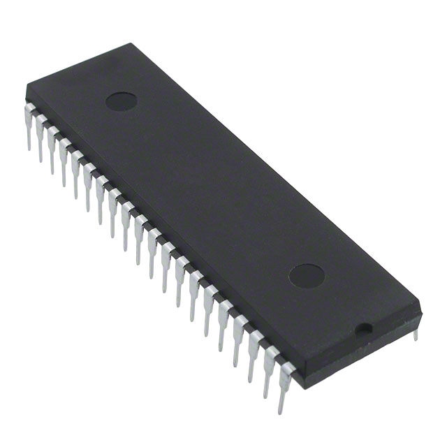
| 描述 | IC USB 4-PORT HUB 40-DIP |
| 产品分类 | |
| 品牌 | Texas Instruments |
| 数据手册 | 点击此处下载产品Datasheethttp://www.ti.com/lit/pdf/mpdi008 |
| 产品图片 |
|
| 产品型号 | TUSB2140BN |
| rohs | 含铅 / 不符合限制有害物质指令(RoHS)规范要求 |
| 产品系列 | - |
| 供应商器件封装 | 40-PDIP |
| 其它名称 | 296-1973 |
| 包装 | 管件 |
| 协议 | USB 1.1 |
| 双工 | - |
| 安装类型 | 通孔 |
| 封装/外壳 | 40-DIP(0.600",15.24mm) |
| 工作温度 | 0°C ~ 70°C |
| 接收器滞后 | 700mV |
| 数据速率 | - |
| 标准包装 | 10 |
| 电压-电源 | 3 V ~ 5.25 V |
| 类型 | 收发器 |
| 驱动器/接收器数 | 1/1 |


PDF Datasheet 数据手册内容提取
TUSB2140B Data Manual 4-Port Hub With an Embedded Function for the Universal Serial Bus SLLS313A March 1999
IMPORTANT NOTICE Texas Instruments and its subsidiaries (TI) reserve the right to make changes to their products or to discontinue any product or service without notice, and advise customers to obtain the latest version of relevant information to verify, before placing orders, that information being relied on is current and complete. All products are sold subject to the terms and conditions of sale supplied at the time of order acknowledgement, including those pertaining to warranty, patent infringement, and limitation of liability. TI warrants performance of its semiconductor products to the specifications applicable at the time of sale in accordance with TI’s standard warranty. Testing and other quality control techniques are utilized to the extent TI deems necessary to support this warranty. Specific testing of all parameters of each device is not necessarily performed, except those mandated by government requirements. CERTAIN APPLICATIONS USING SEMICONDUCTOR PRODUCTS MAY INVOLVE POTENTIAL RISKS OF DEATH, PERSONAL INJURY, OR SEVERE PROPERTY OR ENVIRONMENTAL DAMAGE (“CRITICAL APPLICATIONS”). TI SEMICONDUCTOR PRODUCTS ARE NOT DESIGNED, AUTHORIZED, OR WARRANTED TO BE SUITABLE FOR USE IN LIFE-SUPPORT DEVICES OR SYSTEMS OR OTHER CRITICAL APPLICATIONS. INCLUSION OF TI PRODUCTS IN SUCH APPLICATIONS IS UNDERSTOOD TO BE FULLY AT THE CUSTOMER’S RISK. In order to minimize risks associated with the customer’s applications, adequate design and operating safeguards must be provided by the customer to minimize inherent or procedural hazards. TI assumes no liability for applications assistance or customer product design. TI does not warrant or represent that any license, either express or implied, is granted under any patent right, copyright, mask work right, or other intellectual property right of TI covering or relating to any combination, machine, or process in which such semiconductor products or services might be or are used. TI’s publication of information regarding any third party’s products or services does not constitute TI’s approval, warranty or endorsement thereof. Copyright 1999, Texas Instruments Incorporated
Contents Section Title Page 1 Introduction . . . . . . . . . . . . . . . . . . . . . . . . . . . . . . . . . . . . . . . . . . . . . . . . . . . . . . . . . . . . . . . 1–1 1.1 Features . . . . . . . . . . . . . . . . . . . . . . . . . . . . . . . . . . . . . . . . . . . . . . . . . . . . . . . . . . . . . . 1–1 1.1.1 Hub . . . . . . . . . . . . . . . . . . . . . . . . . . . . . . . . . . . . . . . . . . . . . . . . . . . . . . . . . . . . 1–1 1.1.2 Embedded Function . . . . . . . . . . . . . . . . . . . . . . . . . . . . . . . . . . . . . . . . . . . . . . 1–2 1.1.3 General Characteristics . . . . . . . . . . . . . . . . . . . . . . . . . . . . . . . . . . . . . . . . . . . 1–2 1.2 Terminal Assignments . . . . . . . . . . . . . . . . . . . . . . . . . . . . . . . . . . . . . . . . . . . . . . . . . . 1–2 1.3 Terminal Functions . . . . . . . . . . . . . . . . . . . . . . . . . . . . . . . . . . . . . . . . . . . . . . . . . . . . . 1–3 1.4 Device-Numbering Convention and Ordering Information . . . . . . . . . . . . . . . . . . . 1–5 1.5 Related Documents Referenced . . . . . . . . . . . . . . . . . . . . . . . . . . . . . . . . . . . . . . . . . 1–5 2 Functional Description . . . . . . . . . . . . . . . . . . . . . . . . . . . . . . . . . . . . . . . . . . . . . . . . . . . . . 2–1 2.1 Functional Block Diagram . . . . . . . . . . . . . . . . . . . . . . . . . . . . . . . . . . . . . . . . . . . . . . . 2–1 2.2 USB Transceiver. . . . . . . . . . . . . . . . . . . . . . . . . . . . . . . . . . . . . . . . . . . . . . . . . . . . . . . 2–1 2.3 Clock Generator . . . . . . . . . . . . . . . . . . . . . . . . . . . . . . . . . . . . . . . . . . . . . . . . . . . . . . . 2–1 2.4 Serial Interface Engine (SIE) . . . . . . . . . . . . . . . . . . . . . . . . . . . . . . . . . . . . . . . . . . . . 2–2 2.5 SIE Interface Logic . . . . . . . . . . . . . . . . . . . . . . . . . . . . . . . . . . . . . . . . . . . . . . . . . . . . . 2–2 2.6 Hub Command Decoder . . . . . . . . . . . . . . . . . . . . . . . . . . . . . . . . . . . . . . . . . . . . . . . . 2–2 2.7 Frame Timer . . . . . . . . . . . . . . . . . . . . . . . . . . . . . . . . . . . . . . . . . . . . . . . . . . . . . . . . . . 2–2 2.8 Suspend/Resume Logic . . . . . . . . . . . . . . . . . . . . . . . . . . . . . . . . . . . . . . . . . . . . . . . . 2–2 2.9 Hub Repeater . . . . . . . . . . . . . . . . . . . . . . . . . . . . . . . . . . . . . . . . . . . . . . . . . . . . . . . . . 2–2 2.10 Port Logic. . . . . . . . . . . . . . . . . . . . . . . . . . . . . . . . . . . . . . . . . . . . . . . . . . . . . . . . . . . . . 2–2 2.11 Power Control Logic. . . . . . . . . . . . . . . . . . . . . . . . . . . . . . . . . . . . . . . . . . . . . . . . . . . . 2–2 2.12 Embedded Function Control Logic . . . . . . . . . . . . . . . . . . . . . . . . . . . . . . . . . . . . . . . 2–3 2.13 Embedded Function Control/Status Registers . . . . . . . . . . . . . . . . . . . . . . . . . . . . . 2–3 2.14 Embedded Function FIFOs. . . . . . . . . . . . . . . . . . . . . . . . . . . . . . . . . . . . . . . . . . . . . . 2–3 2.15 Embedded Function I2C Interface . . . . . . . . . . . . . . . . . . . . . . . . . . . . . . . . . . . . . . . . 2–3 3 Internal Registers . . . . . . . . . . . . . . . . . . . . . . . . . . . . . . . . . . . . . . . . . . . . . . . . . . . . . . . . . 3–1 3.1 Address Map . . . . . . . . . . . . . . . . . . . . . . . . . . . . . . . . . . . . . . . . . . . . . . . . . . . . . . . . . . 3–2 3.2 Register Functional Description . . . . . . . . . . . . . . . . . . . . . . . . . . . . . . . . . . . . . . . . . . 3–4 3.2.1 Interrupt Register . . . . . . . . . . . . . . . . . . . . . . . . . . . . . . . . . . . . . . . . . . . . . . . . 3–4 3.2.2 Interrupt Mask Register . . . . . . . . . . . . . . . . . . . . . . . . . . . . . . . . . . . . . . . . . . . 3–5 3.2.3 Function Address Register . . . . . . . . . . . . . . . . . . . . . . . . . . . . . . . . . . . . . . . . 3–5 3.2.4 Endpoint 0 Transmit FIFO . . . . . . . . . . . . . . . . . . . . . . . . . . . . . . . . . . . . . . . . . 3–6 3.2.5 Endpoint 0 Transmit Byte Count Register . . . . . . . . . . . . . . . . . . . . . . . . . . . 3–6 3.2.6 Endpoint 0 Transmit Control Register . . . . . . . . . . . . . . . . . . . . . . . . . . . . . . . 3–7 3.2.7 Endpoint 0 Transmit Status Register. . . . . . . . . . . . . . . . . . . . . . . . . . . . . . . . 3–8 3.2.8 Endpoint 0 Transmit FIFO Flags Register . . . . . . . . . . . . . . . . . . . . . . . . . . . 3–9 3.2.9 Endpoint 0 Receive FIFO . . . . . . . . . . . . . . . . . . . . . . . . . . . . . . . . . . . . . . . . . 3–9 3.2.10Endpoint 0 Receive Byte Count Register . . . . . . . . . . . . . . . . . . . . . . . . . . . . 3–9 iii
3.2.11Endpoint 0 Receive Control Register . . . . . . . . . . . . . . . . . . . . . . . . . . . . . . 3–10 3.2.12Endpoint 0 Receive Status Register . . . . . . . . . . . . . . . . . . . . . . . . . . . . . . . 3–11 3.2.13Endpoint 0 Receive FIFO Flags Register . . . . . . . . . . . . . . . . . . . . . . . . . . . 3–12 3.2.14Endpoint 1 Transmit FIFO . . . . . . . . . . . . . . . . . . . . . . . . . . . . . . . . . . . . . . . . 3–12 3.2.15Endpoint 1 Transmit Byte Count Register . . . . . . . . . . . . . . . . . . . . . . . . . . 3–12 3.2.16Endpoint 1 Transmit Control Register . . . . . . . . . . . . . . . . . . . . . . . . . . . . . . 3–13 3.2.17Endpoint 1 Transmit Status Register. . . . . . . . . . . . . . . . . . . . . . . . . . . . . . . 3–14 3.2.18Endpoint 1 Transmit FIFO Flags Register . . . . . . . . . . . . . . . . . . . . . . . . . . 3–15 3.2.19PID Low-Byte Register . . . . . . . . . . . . . . . . . . . . . . . . . . . . . . . . . . . . . . . . . . 3–15 3.2.20PID High-Byte Register . . . . . . . . . . . . . . . . . . . . . . . . . . . . . . . . . . . . . . . . . . 3–16 3.2.21VID Low-Byte Register . . . . . . . . . . . . . . . . . . . . . . . . . . . . . . . . . . . . . . . . . . 3–16 3.2.22VID High-Byte Register . . . . . . . . . . . . . . . . . . . . . . . . . . . . . . . . . . . . . . . . . . 3–16 4 Device Operation . . . . . . . . . . . . . . . . . . . . . . . . . . . . . . . . . . . . . . . . . . . . . . . . . . . . . . . . . . 4–1 4.1 Device Initialization . . . . . . . . . . . . . . . . . . . . . . . . . . . . . . . . . . . . . . . . . . . . . . . . . . . . 4–1 4.2 Hub . . . . . . . . . . . . . . . . . . . . . . . . . . . . . . . . . . . . . . . . . . . . . . . . . . . . . . . . . . . . . . . . . . 4–1 4.3 Embedded Function . . . . . . . . . . . . . . . . . . . . . . . . . . . . . . . . . . . . . . . . . . . . . . . . . . . . 4–1 4.3.1 Interrupt Handler. . . . . . . . . . . . . . . . . . . . . . . . . . . . . . . . . . . . . . . . . . . . . . . . . 4–1 4.3.2 Function Reset and USB Reset . . . . . . . . . . . . . . . . . . . . . . . . . . . . . . . . . . . . 4–1 4.3.3 Enumeration . . . . . . . . . . . . . . . . . . . . . . . . . . . . . . . . . . . . . . . . . . . . . . . . . . . . 4–2 4.3.4 Control Transfers . . . . . . . . . . . . . . . . . . . . . . . . . . . . . . . . . . . . . . . . . . . . . . . . 4–2 4.3.5 Interrupt Transfers . . . . . . . . . . . . . . . . . . . . . . . . . . . . . . . . . . . . . . . . . . . . . . . 4–2 4.3.6 Suspend and Remote Wake-Up . . . . . . . . . . . . . . . . . . . . . . . . . . . . . . . . . . . 4–3 4.3.7 I2C Interface . . . . . . . . . . . . . . . . . . . . . . . . . . . . . . . . . . . . . . . . . . . . . . . . . . . . 4–3 4.4 Over-Current Detection and Power Switching . . . . . . . . . . . . . . . . . . . . . . . . . . . . . . 4–5 4.5 Clock Output Generation. . . . . . . . . . . . . . . . . . . . . . . . . . . . . . . . . . . . . . . . . . . . . . . . 4–5 4.6 Power Supply Sequencing . . . . . . . . . . . . . . . . . . . . . . . . . . . . . . . . . . . . . . . . . . . . . . 4–6 5 Electrical Specifications . . . . . . . . . . . . . . . . . . . . . . . . . . . . . . . . . . . . . . . . . . . . . . . . . . . 5–1 5.1 Absolute Maximum Ratings Over Operating Free-air Temperature Range . . . . . 5–1 5.2 Recommended Operating Conditions . . . . . . . . . . . . . . . . . . . . . . . . . . . . . . . . . . . . . 5–1 5.3 Electrical Characteristics Over Recommended Ranges of Operating Free-air Temperature and Supply Voltage. . . . . . . . . . . . . . . . . . . . . . . . . . . . . . . . . . . . . . . . . 5–2 5.4 Timing Characteristics . . . . . . . . . . . . . . . . . . . . . . . . . . . . . . . . . . . . . . . . . . . . . . . . . . 5–3 5.4.1 Timing Characteristics for USB Transceivers . . . . . . . . . . . . . . . . . . . . . . . . 5–3 5.4.2 Timing Characteristics for I2C Interface . . . . . . . . . . . . . . . . . . . . . . . . . . . . . 5–5 5.4.3 Timing Characteristics for Remote Wake-Up. . . . . . . . . . . . . . . . . . . . . . . . . 5–7 6 USB Overview Description . . . . . . . . . . . . . . . . . . . . . . . . . . . . . . . . . . . . . . . . . . . . . . . . . 6–1 6.1 Application Information . . . . . . . . . . . . . . . . . . . . . . . . . . . . . . . . . . . . . . . . . . . . . . . . . 6–2 6.2 Bus-Powered Hub, Ganged Port Power Management . . . . . . . . . . . . . . . . . . . . . . 6–4 6.3 Self-Powered Hub, Ganged Port Power Management . . . . . . . . . . . . . . . . . . . . . . 6–5 6.4 Self-Powered Hub, Individual Port Power Management . . . . . . . . . . . . . . . . . . . . . 6–6 Appendix A Firmware Development . . . . . . . . . . . . . . . . . . . . . . . . . . . . . . . . . . . . . . . . . . . . A–1 Appendix B Firmware Example . . . . . . . . . . . . . . . . . . . . . . . . . . . . . . . . . . . . . . . . . . . . . . . . . B–1 Appendix C Flow Chart for the Firmware Sample Code . . . . . . . . . . . . . . . . . . . . . . . . . . C–1 Appendix D Mechanical Data . . . . . . . . . . . . . . . . . . . . . . . . . . . . . . . . . . . . . . . . . . . . . . . . . . D–1 iv
List of Illustrations Figure Title Page 5–1 Differential Driver Switching Load . . . . . . . . . . . . . . . . . . . . . . . . . . . . . . . . . . . . . . . . . 5–3 5–2 USB Data Signal Rise and Fall Times . . . . . . . . . . . . . . . . . . . . . . . . . . . . . . . . . . . . . . 5–4 5–3 Differential Receiver Input Sensitivity vs Common Mode Input Range . . . . . . . . . . 5–4 5–4 Single-Ended Receiver Input Signal Parameter Definitions . . . . . . . . . . . . . . . . . . . 5–5 5–5 SCL and SDA Timing . . . . . . . . . . . . . . . . . . . . . . . . . . . . . . . . . . . . . . . . . . . . . . . . . . . . 5–5 5–6 Start and Stop Conditions . . . . . . . . . . . . . . . . . . . . . . . . . . . . . . . . . . . . . . . . . . . . . . . . 5–5 5–7 Output Acknowledge . . . . . . . . . . . . . . . . . . . . . . . . . . . . . . . . . . . . . . . . . . . . . . . . . . . . 5–6 5–8 Single Byte Write Transfer. . . . . . . . . . . . . . . . . . . . . . . . . . . . . . . . . . . . . . . . . . . . . . . . 5–6 5–9 Multiple Byte Write Transfer . . . . . . . . . . . . . . . . . . . . . . . . . . . . . . . . . . . . . . . . . . . . . . 5–6 5–10 Single Byte Read Transfer . . . . . . . . . . . . . . . . . . . . . . . . . . . . . . . . . . . . . . . . . . . . . . . 5–7 5–11 Multiple Byte Read Transfer . . . . . . . . . . . . . . . . . . . . . . . . . . . . . . . . . . . . . . . . . . . . . . 5–7 5–12 Remote Wake-Up . . . . . . . . . . . . . . . . . . . . . . . . . . . . . . . . . . . . . . . . . . . . . . . . . . . . . . . 5–7 6–1 USB Tiered Configuration Example . . . . . . . . . . . . . . . . . . . . . . . . . . . . . . . . . . . . . . . . 6–1 6–2 Typical I2C Interface Connection to a Microcontroller . . . . . . . . . . . . . . . . . . . . . . . . 6–2 6–3 Resonator Clock Circuit . . . . . . . . . . . . . . . . . . . . . . . . . . . . . . . . . . . . . . . . . . . . . . . . . 6–2 6–4 Crystal Tuning Circuit . . . . . . . . . . . . . . . . . . . . . . . . . . . . . . . . . . . . . . . . . . . . . . . . . . . . 6–3 6–5 TUSB2140B Bus-Powered Hub, Ganged Port Power Management Application . . 6–4 6–6 TUSB2140B Self-Powered Hub, Ganged Port Power Management Application . . 6–5 6–7 TUSB2140B Self-Powered Hub, Individual-Port Power Management Application . . . . . . . . . . . . . . . . . . . . . . . . . . . . . . . . . . . . . . . . . . . . . . . . . . . . . . . . . . . . . 6–6 A–1 Flow Chart for TUSB2140B Firmware . . . . . . . . . . . . . . . . . . . . . . . . . . . . . . . . . . . . . A–2 A–2 Endpoint 0 Transmit Interrupt Service Routine . . . . . . . . . . . . . . . . . . . . . . . . . . . . . . A–3 A–3 Endpoint 0 Receive Interrupt Service Routine . . . . . . . . . . . . . . . . . . . . . . . . . . . . . . A–5 A–4 Endpoint 1 Transmit Interrupt Service Routine . . . . . . . . . . . . . . . . . . . . . . . . . . . . . . A–6 C–1 Flow Chart for TUSB2140B Firmware (Sample Code) . . . . . . . . . . . . . . . . . . . . . . . . C–1 C–2 Endpoint 0 Receive Interrupt Service Routine . . . . . . . . . . . . . . . . . . . . . . . . . . . . . . C–2 C–3 Endpoint 0 Transmit Interrupt Service Routine . . . . . . . . . . . . . . . . . . . . . . . . . . . . . . C–3 v
vi
1 Introduction The TUSB2140B is a compound USB device that provides an external 4-port hub and an embedded function that is virtually connected to an internal fifth hub port. The TUSB2140B is fully compatible with the USB, version 1.0, specification and the embedded function is fully compatible with the USB display-device class specification. The USB hub has a control endpoint and an interrupt endpoint. The embedded function also includes a control endpoint and an interrupt endpoint to support USB data transfers. The FIFOs and control registers associated with the endpoints are fully integrated within the device. An Inter IC(I2C), 2-wire serial bus provides an interface for any local micro-controller unit (MCU) to access the FIFOs and control registers. The TUSB2140B hub has the default power-on vendor ID (VID) of 0451H and a product ID (PID) of 2140H for the hub which will be displayed as General-Purpose USB Hub during enumeration. When custom vendor and product ID’s are desired for the external 4-port USB hub, the default VID/PID values can be replaced with custom values that are firmware based. When new VID/PID values are desired, they must be down-loaded through the I2C interface before the MCU connects the embedded function. The VID and PID for the embedded functions are always firmware based. The TUSB2140B hub supports power switching to the downstream ports for either individual or ganged power management modes. External power-management devices are required to switch power and to detect over-current conditions. See Application Information in Section 6. The TUSB2140B provides the required inputs and outputs needed for the power-management devices to control power switching and to monitor any over-current conditions. In the ganged mode, all PWRON signals switch simultaneously and all OVRCUR inputs should be tied together and driven by the same signal. The TUSB2140B requires a 48-MHz clock signal to sample data from the upstream port and to generate a synchronized 12-MHz USB clock signal. The hub supports the flexibility to use either a 48-MHz oscillator, a 48-MHz resonator, or a crystal tuned to 48-MHz. When an oscillator is used, the oscillator output must be connected to the XTAL1 terminal and the XTAL2 terminal should remain open. An oscillator with a TTL level output may be used if the output does not exceed 3.6-V maximum. When an oscillator is used, the TUSB2140B device will not be able to go into low-power suspend mode because the oscillator will always drive a 48-MHz clock signal into the TUSB2140B. A better implementation is to use a passive device such as a resonator or a crystal because when the TUSB2140B suspends, the resonator and crystal will also stop operation. For a resonator or crystal implementation, the XTAL1 terminal should be used as the input and the XTAL2 terminal should be used as the feedback path. See Figure 6–3 for resonator connection. Because the crystal is required to resonate at 48-MHz, a tuning circuit may be required such as shown in Figure 6–4. USB-compatible transceivers are provided for all upstream and downstream ports. All external downstream ports support both full-speed and low-speed connections by automatically setting the slew rate according to the speed of the device attached to the port. 1.1 Features The main features of the TUSB2140B hub and embedded function are listed in the following sections. 1.1.1 Hub • Universal Serial Bus (USB) Version 1.0 Compatible • Includes Serial Interface Engine (SIE) • All Four External Downstream Ports Support Full-Speed and Low-Speed Operations • Integrated USB Transceivers • Power Switching and Over-Current Conditions are Reported for Per Port or Ganged Modes • Supports default or custom Product ID (PID) and Vendor ID (VID) 1–1
1.1.2 Embedded Function • USB Display Class Compatible • Supports both Control and Interrupt Data Transfers • Integrated FIFOs and Control/Status Registers • Supports Interrupt Driven Operation to Minimize Local Micro-Controller Polling • Supports USB Remote Wake-Up • Supports Custom Product ID (PID) and Vendor ID (VID) 1.1.3 General Characteristics • Low-Power CMOS Technology • Generates a Clock Output With a Frequency of 12 MHz, 8 MHz, 6 MHz, or 4 MHz • Available in a 40-Pin Dip Package or a 44-Pin LQFP Package • Requires a 48-MHz Crystal, a 48–MHz Resonator, or 48-MHz Oscillator Input • Uses a 3.3 V and 5 V Power Supply 1.2 Terminal Assignments N PACKAGE (TOP VIEW) WAKEUP 1 40 VCC5V CLKOUT 2 39 SCL GND 3 38 SDA CLKSEL0 4 37 IRQ CLKSEL1 5 36 PWRON5 OVRCUR5 6 35 FUNCSUSP OVRCUR2 7 34 PWRON2 PWRON1 8 33 VCC3V OVRCUR1 9 32 OVRCUR3 DP0 10 31 PWRON3 DM0 11 30 GND GND 12 29 XTAL1 DP1 13 28 XTAL2 DM1 14 27 OSCOFF BUSPWR 15 26 PWRON4 GANGED 16 25 OVRCUR4 DP2 17 24 RESET DM2 18 23 DM4 V 3V 19 22 DP4 CC DP3 20 21 DM3 1–2
PGT PACKAGE (TOP VIEW) NCCLKSEL1 CLKSEL0 GND CLKOUT WAKEUP V 5VCCSCL SDA RQ PWRON5 I 44 4342 41 40 3938 3736 35 34 OVRCUR5 1 33 NC OVRCUR2 2 32 FUNCSUSP PWRON1 3 31 PWRON2 OVRCUR1 4 30 VCC3V DP0 5 29 OVRCUR3 DM0 6 28 PWRON3 GND 7 27 GND DP1 8 26 XTAL1 DM1 9 25 XTAL2 BUSPWR 10 24 OSCOFF NC 11 23 PWRON4 1213 14 1516 17 1819 20 21 22 D2 2 V 3 3 44 T 4 C EP M 3 P M PM E R N ANGD D V CCD D DD RES RCU G V O NC – No internal connection 1.3 Terminal Functions TERMINAL PGT N I/O DESCRIPTION NAME NO. NO. BUSPWR 10 15 I Port power indicator. BUSPWR is an active low input that indicates whether the ports and the hub source power from the USB bus or are self-powered by the local power supply. When a microcontroller is connected to the TUSB2140B, the hub must be self-powered and it is mandatory for this pin to be connected to 3.3 V. This standard TTL input must not change dynamically during operation. CLKOUT 40 2 O Clock output. Depending on the configuration of CLKSEL0 and CLKSEL1, CLKOUT is a selected clock output of 12 MHz, 8 MHz, 6 MHz, or 4 MHz. DM1 – DM4 9, 14, 14, 18, I/O Data minus USB differential data pairs. DM1 – DM4 support up to four 17, 19 21, 23 negative-signal downstream USB ports. DP1 – DP4 8, 13, 13, 17, I/O Data plus USB differential data pairs. DP1 – DP4 support up to four 16, 18 20, 22 positive-signal downstream USB ports. DM0 6 11 I/O Data minus USB differential data. DM0 is used for the upstream USB port cable pair and negative signal. DP0 5 10 I/O Data plus USB differential data. DP0 is used for the upstream USB port cable pair and positive signal. 1–3
1.3 Terminal Functions (continued) TERMINAL PGT N I/O DESCRIPTION NAME NO. NO. FUNCSUSP 32 35 O Function port suspend. FUNCSUSP is an active high output that indicates if the port that connects to the embedded function has been selectively suspended. See Suspend and Remote Wake-Up in section 4.3.6 for further information. GANGED 12 16 I Power switch/over-current detection mode select. GANGED selects between gang or per port switching for over-current detection of the downstream ports. This pin should be set dependent upon how the external power management devices are configured. This standard TTL input must not change dynamically during operation. GND 7, 27, 3, 12, Ground. All terminals must be tied to ground for proper operation. 41 30 IRQ 35 37 O Interrupt. IRQ is an active low output to the micro-controller that indicates an interrupt condition has occurred. OSCOFF 24 27 I Oscillator off. OSCOFF disables the internal oscillator for quiescent current draw (ICCQ) testing. OSCOFF must be tied low for normal operation. OVRCUR1 – 4, 2, 29, 9, 7, 32, I Over-current indicators. OVRCUR1 – OVRCUR5 are active low, standard OVRCUR5 21, 1 25, 6 TTL inputs. One over-current indicator is available for each of the four downstream ports. These inputs are internally gated when port power switching is ganged. The unused terminals must be tied high. PWRON1 – 3, 31, 8, 34, O Power on/off control switches. PWRON1 – PWRON5 are active low, PWRON5 28, 23, 31, 26, open-drain outputs. One power on/off control switch is used for each of 34 36 the four downstream ports. All outputs are switched together when the port power switching is ganged. RESET 20 24 I Reset. RESET is a TTL input with hysteresis and must be asserted at power up for conformance to USB. RESET is an active low and must be asserted for at least 250 ns for all logic to be properly re-initialized. However, asserting the RESET for longer than 5 ms could cause the TUSB2140B to NAK too long and be ignored by the USB host. SCL 37 39 I Serial clock. SCL is the clock signal for the I2C serial interface and is 5-V tolerant. SDA 36 38 I/O Serial data. SDA is the bidirectional data signal for the I2C serial interface and is 5-V tolerant. SDA uses an open-drain output driver. VCC3V 15, 30 19, 33 3.3-V supply voltage VCC5V 38 40 5-V supply voltage WAKEUP 39 1 I Function port remote wake-up. WAKEUP is an active high input used by the micro-controller to initiate a remote wake-up from a suspended mode. WAKEUP is 5-V tolerant. See Suspend and Remote Wake-Up in section 4.3.6 for further information. XTAL1 26 29 I Crystal 1. XTAL1 is a 48-MHz clock input. Operation at 48-MHz is four times the USB full-speed bit rate of 12 Mbps. XTAL2 25 28 O Crystal 2. XTAL2 is a 48-MHz feedback output for crystals and resonators. Operation at 48-MHz is four times the USB full-speed bit rate of 12 Mbps. CLKSEL0, 42, 43 4, 5 I Clock select inputs. CLKSEL0 and CLKSEL1 determine the CLKOUT CLKSEL1 frequency (See Table 4–2). 1–4
1.4 Device-Numbering Convention and Ordering Information T USB 2 1 40 B N Texas Instruments Universal Serial Bus Hub Device Hub Generation Type 2 1 = Embedded Function with I C 0 = Pure Hub Number of Downstream Ports 40 = 4 Downstream USB Ports Version Number Package Type PDIP 40 pins N LQFP 44 pins PGT 1.5 Related Documents Referenced • Universal Serial Bus Specification version 1.0 dated January 19, 1996. • Inter IC (I2C) Specification 1–5
1–6
2 Functional Description The functional block diagram for the TUSB2140B is shown in Section 2.1. The description for the function blocks follow Section 2.1. For additional information, including USB signaling specifications, packet protocol, and hub functionality, please refer to the Universal Serial Bus Specification version 1.0 dated January 19, 1996. 2.1 Functional Block Diagram DP0 DM0 10 11 USB Transceiver 27 OSCOFF 29, 28 XTAL1, XTAL2 4, 5 Clock CLKSEL0, CLKSEL1 Suspend/Resume 2 Generator CLKOUT Hub Repeater Logic and SIE 24 State Machine and Frame Timer RESET Signal Router 1 WAKEUP 35 FUNCSUSP 38 SIE Interface I2C 39 SDA FIFOs SCL Logic Slave 37 IRQ Port 1 Logic Function Control Control Status Logic Registers Port 4 Hub/Device Logic Command Embedded Function Decoder USB USB Transceiver Transceiver 16 GANGED 22 23 13 14 15 Power Control Logic BUSPWR 9, 7, 32, 25, 6 DP4 DM4 DP1 DM1 OVRCUR1 – OVRCUR5 8, 34, 31, 26, 36 PWRON1 – PWRON5 NOTE A: Terminal numbers shown are for the N package 2.2 USB Transceiver The TUSB2140B provides integrated transceivers for all the USB ports. The transceivers include a differential output driver, a differential input receiver and two single ended inputs. The transceiver for each port connects to the appropriate DP and DM differential signal pair. 2.3 Clock Generator Utilizing the 48-MHz input signal, the clock generator logic generates the CLKOUT output signal in addition to the various internal clock signals. The TUSB2140B internal clocks consist of the 48-MHz clock, a 12-MHz clock, and a USB clock. The USB clock also has a frequency of 12-MHz. The USB clock is the same as the 12-MHz clock when the TUSB2140B is transmitting data and is derived from the data when the TUSB2140B is receiving data. 2–1
2.4 Serial Interface Engine (SIE) The serial interface engine logic manages the USB packet protocol requirements for the packets being received and transmitted by the TUSB2140B. For packets being received, the SIE decodes the packet identifier field (PID) to determine the type of packet being received and ensures the PID is valid. For token packets and data packets being received, the SIE calculates the packet CRC and compares the value to the CRC contained in the packet to verify that the packet was not corrupted during transmission. For token packets and data packets being transmitted, the SIE generates the CRC that is transmitted with the packet. For packets being transmitted, the SIE also generates the synchronization field (SYNC) which is the eight bit field at the beginning of each packet. In addition, the SIE generates the correct PID for all packets being transmitted. Another major function of the SIE is the overall serial-to-parallel conversion of the data packets being received and the parallel-to-serial conversion of the data packets being transmitted. 2.5 SIE Interface Logic The SIE interface logic provides the control logic that interfaces the SIE to the hub control logic and the embedded function control logic. One of the major functions of the SIE interface logic is to decode the function address from the SIE to determine if either the hub or embedded function is being addressed. In addition, the endpoint address field is decoded to determine which particular endpoint of the hub or embedded function is being addressed. The SIE interface logic also managers the multiplexing of the byte-wide transmit data signals and other control signals from the hub control logic and embedded function control logic. 2.6 Hub Command Decoder The hub command decoder logic manages the overall control of the hub including the decode and execution of host initiated control commands, as well as the status change endpoint. During USB interrupt transfers, the USB host uses the status change endpoint to acquire hub status and port status change information. 2.7 Frame Timer The frame timer logic generates the end of frame (EOF) signal which is used mainly to ensure that all downstream traffic is completed during each frame period. In addition, since the frame timer counts 1.0 ms periods, the EOF signal is used by other logic that needs to time events based on multiples of 1.0 ms periods. The hub frame timer logic is locked to the host frame timer logic by the host generated Start of Frame (SOF) packets. 2.8 Suspend/Resume Logic The suspend/resume logic is used to detect the suspend/resume states and to generate the signals used to control the overall device during the suspend/resume states. See Suspend and Remote Wake-Up in section 4.3.6 for further information. 2.9 Hub Repeater The hub repeater logic manages the connectivity of the root port and the downstream ports on a per-packet basis. The data flow of the USB packets through the TUSB2140B from the root port to the downstream ports and vice-a-versa is totally asynchronous. 2.10 Port Logic The port logic manages the overall state of a particular downstream port. Each downstream port has unique port logic which controls the connect/disconnect, enable/disable, suspend/resume and reset states of the port. 2.11 Power Control Logic The power control logic generates the PWRON1 thru PWRON5 output signals based on the GANGED, BUSPWR, and OVRCUR input signals. 2–2
2.12 Embedded Function Control Logic The Function control logic (FCL) manages communication between the local microcontroller Unit (MCU) and the Serial interface engine (SIE). The local MCU directs the operation of the FCL through the control and status registers. One of the major functions performed by the FCL is to move data to and from the internal FIFOs during the control and interrupt endpoint transfer operations. 2.13 Embedded Function Control/Status Registers The control and status registers allow the local MCU to control and monitor transfer operations done by the TUSB2140B. A separate set of registers is used to control the transmit and receive operations for the control endpoint which is endpoint 0. In addition, a separate set of registers is provided for the interrupt endpoint transmit operations, which is endpoint 1. Also, an interrupt and interrupt mask register is provided to control the conditions that generate the IRQ output signal. 2.14 Embedded Function FIFOs The TUSB2140B internal FIFOs provide a buffer between the SIE and the local MCU. There are three 8-byte by 8-bit FIFOs provided. There is a separate transmit and receive FIFO provided for the control endpoint, which is endpoint 0. In addition, there is a transmit FIFO provided for the interrupt endpoint, which is endpoint 1. 2.15 Embedded Function I2C Interface The I2C Interface logic provides a two-wire serial interface that is used by a local MCU or device needing serial access to the TUSB2140B control/status registers and FIFOs. The interface allows single byte read and writes to the registers and multiple byte read and writes to the FIFOs. Note that the transmit FIFOs are write only and the receive FIFOs are read only from the local MCU side. 2–3
2–4
3 Internal Registers The TUSB2140B provides a set of control and status registers to be used by the local microcontroller unit to control the overall operation of the embedded function. The control and status registers allow the local MCU to control and monitor USB transfers to both the control endpoint and the interrupt endpoint of the embedded function. There is a separate set of registers provided for the control endpoint transmit and receive operations. In addition, there is a separate set of registers provided for the transmit operations of the interrupt endpoint. Also, an interrupt and interrupt mask register is provided to control the conditions that generate the IRQ output signal. 3–1
3 3.1 Address Map – 2 MSB LSB AADDDDRREESSSS NNAAMMEE 7 6 5 4 3 2 1 0 00h FSUSP FRST EP1TX EP0RX EP0TX Interrupt Register 01h FSUSP FRST EP1TX EP0RX EP0TX Interrupt Mask Register 02h FEN FA6 FA5 FA4 FA3 FA2 FA1 FA0 Function Address Register 03h 04h D7 D6 D5 D4 D3 D2 D1 D0 EP0 TX FIFO 05h BCNT3 BCNT2 BCNT1 BCNT0 EP0 TX Byte Count Register 06h TXCLR TXSTL TXFEN TXEN EP0 TX Control Register 07h TXSEQ STSGE STALL NACK ERROR ACK EP0 TX Status Register 08h EMPT FULL UNDR OVRR EP0 TX FIFO Flags Register 09h D7 D6 D5 D4 D3 D2 D1 D0 EP0 RX FIFO 0Ah BCNT3 BCNT2 BCNT1 BCNT0 EP0 RX Byte Count Register 0Bh RXCLR RXSTL RXFEN RXEN EP0 RX Control Register 0Ch RXSEQ SETUP RXFSW STSGE STALL NACK ERROR ACK EP0 RX Status Register 0Dh EMPT FULL UNDR OVRR EP0 RX FIFO Flags Register 0Eh 0Fh 10h D7 D6 D5 D4 D3 D2 D1 D0 EP1 TX FIFO 11h BCNT3 BCNT2 BCNT1 BCNT0 EP1 TX Byte Count Register 12h TXCLR TXSOW TXSTL TXFEN TXEN EP1 TX Control Register 13h TXSEQ STALL NACK ERROR ACK EP1 TX Status Register 14h EMPT FULL UNDR OVRR EP1 TX FIFO Flags Register 15h PID(7) PID(6) PID(5) PID(4) PID(3) PID(2) PID(1) PID(0) Hub Product ID, Low Byte Register 16h PID(15) PID(14) PID(13) PID(12) PID(11) PID(10) PID(9) PID(8) Hub Product ID, High Byte Register 17h VID(7) VID(6) VID(5) VID(4) VID(3) VID(2) VID(1) VID(0) Hub Vendor ID, Low Byte Register 18h VID(15) VID(14) VID(13) VID(12) VID(11) VID(10) VID(9) VID(8) Hub Vendor ID, High Byte Register 19h
3.1 Address Map (continued) MSB LSB AADDDDRREESSSS NNAAMMEE 7 6 5 4 3 2 1 0 1Ah 1Bh 1Ch 1Dh 1Eh 1Fh 3 – 3
3.2 Register Functional Description The following sections contain the functional descriptions for each register and the individual register bits. Note that firmware should write a 0 to reserved bits and ignore any value read from reserved bits. 3.2.1 Interrupt Register The interrupt register bits are used to indicate when an interrupt condition is pending. If one or more of the interrupt bits are set, the TUSB2140B interrupt output signal (IRQ) will be asserted until the interrupt condition(s) is cleared. One or more of the interrupt bits can be masked by setting the corresponding bit in the interrupt mask register. If the interrupt mask bit is set, the corresponding interrupt bit will still be set when an interrupt condition occurs. However, the IRQ output signal will not be asserted. This feature is provided for systems that detect pending interrupt conditions with a polling scheme rather than by monitoring the IRQ output signal. 7 0 – – – FSUSP FRST EP1TX EP0RX EP0TX BIT MNEMONIC NAME DESCRIPTION 7:5 – Reserved Reserved for future use. 4 FSUSP Function suspend The function suspend interrupt bit is set in response to the hub suspend logic detecting a global suspend condition or a selective suspend condition for the embedded function. To enable the TUSB2140B to enter a low–power suspend state which includes disabling the clocks, this bit must be cleared by the local MCU. This bit is cleared by writing a 1 to this register. This bit is read/write and is cleared by power-on reset. 3 FRST Function reset The function reset interrupt bit is set in response to the host initiating a port reset on the function port. To enable the function reset, this bit must be cleared by the local MCU. When a function reset occurs, all of the Function Interface logic within the TUSB2140B will be reset except the endpoint 0 receive enable bit (RXEN), the endpoint 0 transmit enable bit (TXEN), the function reset interrupt bit (FRST) and all of the interrupt mask bits. This bit is cleared by writing a 1 to this register. This bit is read/write and is cleared by power-on reset. 2 EP1TX Endpoint 1 The endpoint 1 transmit interrupt bit is set in response to the endpoint transmit interrupt 1 transmit acknowledge status bit (ACK), the endpoint 1 transmit FIFO over-run flag bit (OVRR), or the endpoint 1 transmit FIFO under-run flag bit (UNDR) being set. This bit is cleared by clearing the corresponding status or FIFO flag bit that caused the interrupt. This bit is read-only and is cleared by power-on reset. 1 EP0RX Endpoint 0 The endpoint 0 receive interrupt bit is set in response to the endpoint 0 receive interrupt receive acknowledge status bit (ACK), the endpoint 0 receive FIFO over-run flag bit (OVRR), or the endpoint 0 receive FIFO under-run flag bit (UNDR) being set. This bit is cleared by clearing the corresponding status or FIFO flag bit that caused the interrupt. This bit is read-only and is cleared by power-on reset. 0 EP0TX Endpoint 0 The endpoint 0 transmit interrupt bit is set in response to the endpoint transmit interrupt 0 transmit acknowledge status bit (ACK), the endpoint 0 transmit FIFO over-run flag bit (OVRR), or the endpoint 0 transmit FIFO under-run flag bit (UNDR) being set. This bit is cleared by clearing the corresponding status or FIFO flag bit that caused the interrupt. This bit is read-only and is cleared by power-on reset. 3–4
3.2.2 Interrupt Mask Register The interrupt mask register bits are used to mask the corresponding interrupt bits. 7 0 – – – FSUSP FRST EP1TX EP0RX EP0TX BIT MNEMONIC NAME DESCRIPTION 7:4 – Reserved Reserved for future use 4 FSUSP Function suspend The function suspend interrupt mask bit is set to interrupt mask enable the function suspend interrupt bit. This bit is read/write and is cleared by power–on reset. 3 FRST Function reset interrupt mask The function reset interrupt mask bit is set to enable the function reset interrupt bit. This bit is read/write and is cleared by power-on reset. 2 EP1TX Endpoint 1 transmit interrupt mask The endpoint 1 transmit interrupt mask bit is set to enable the endpoint 1 transmit interrupt bit. This bit is read/write and is cleared by power-on reset. 1 EP0RX Endpoint 0 receive interrupt mask The endpoint 0 receive interrupt mask bit is set to enable the endpoint 0 receive interrupt bit. This bit is read/write and is cleared by power-on reset. 0 EP0TX Endpoint 0 transmit interrupt mask The endpoint 0 transmit interrupt mask bit is set to enable the endpoint 0 transmit interrupt bit. This bit is read/write and is cleared by power-on reset. 3.2.3 Function Address Register The function address register contains the current setting of the USB device address assigned to the function. During enumeration of the function, the function address is loaded into this register automatically by the TUSB2140B Function Control Logic when a Set Address request is received from the USB host. This register is read only and is used only for diagnostic purposes. 7 0 FEN FA6 FA5 FA4 FA3 FA2 FA1 FA0 BIT MNEMONIC NAME DESCRIPTION 7 FEN Function enabled The function enabled bit is set when the embedded function port has been enabled by the host with a set port feature request. This bit is read-only and is cleared by power-on reset. 6:0 FA(6:0) Function address The function address register value is set to the current device address assigned to the function. These bits are read/write-able and are cleared by power-on reset. The function address is updated when the MCU receives a set-address control transfer for the embedded function from the host. The MCU will then update the function address from the micro-controller firmware through the I2C interface. 3–5
3.2.4 Endpoint 0 Transmit FIFO 7 0 D7 D6 D5 D4 D3 D2 D1 D0 BIT MNEMONIC NAME DESCRIPTION 7:0 D(7:0) Transmit Endpoint 0 transmit FIFO data is written to the transmit FIFO on a byte-to-byte FIFO data basis. These bits are write-only. 3.2.5 Endpoint 0 Transmit Byte Count Register 7 0 – – – – BCNT3 BCNT2 BCNT1 BCNT0 BIT MNEMONIC NAME DESCRIPTION 7:4 – Reserved Reserved for future use. 3:0 BCNT(3:0) Transmit The transmit byte count register should be loaded with the number of bytes to be byte count transmitted. The byte count should be the number of bytes in the data packet that was loaded into the transmit FIFO. When the local MCU writes to the byte count register, the EP0 transmit FIFO enable bit (TXFEN) will automatically be set. Also, the byte count register does not decrement as data is transmitted. These bits are read/write and are cleared by power-on reset. 3–6
3.2.6 Endpoint 0 Transmit Control Register The transmit control register is used to store bits which control various functions and operating modes of the function interface logic within the TUSB2140B. 7 0 TXCLR – – – TXSTL – TXFEN TXEN BIT MNEMONIC NAME DESCRIPTION 7 TXCLR Transmit The transmit clear bit is set to reset the transmit FIFO pointers and flags. This bit clear should be set in response to a transmit FIFO over–run or under-run condition. After the FIFO pointers are reset, this bit will be automatically cleared. In addition, the FIFO empty flag will be set and the other FIFO flags will be cleared upon completion of the FIFO reset. This bit is read/write and is cleared by power-on reset. 6 – Reserved Reserved for future use 5 – Reserved Reserved for future use 4 – Reserved Reserved for future use 3 TXSTL Transmit The transmit stall bit is set to enable a STALL handshake to be returned in stall response to the next valid In Transaction. This bit is automatically cleared if a new Setup Stage Transaction is successfully received. This bit is read/write and is cleared by power-on reset. 2 – Reserved Reserved for future use 1 TXFEN Transmit The transmit FIFO enable bit is set to enable the transmission of data in the FIFO transmit FIFO when the next valid in transaction occurs. This bit is automatically enable set when the local MCU writes to the EP0 transmit byte count register and is automatically cleared when the EP0 transmit acknowledge status bit (ACK) is set. This bit is also automatically cleared if a new setup stage transaction is successfully received or the EP0 transmit clear bit (TXCLR) is set. If the transmit enable bit is not set, the device returns a NACK handshake. If the transmit stall control bit (TXSTL) is set, a STALL handshake is returned instead of a NACK handshake. This bit is read/write and is cleared by power-on reset. 0 TXEN Transmit The transmit enable bit is set to enable the transmit endpoint. For endpoint 0, the enable control endpoint, both a receive and transmit endpoint are required. Therefore, the transmit enable and receive enable bits must both be set before the device will be enumerated. If either of these bits is not set, the function port will remain in the disconnected state. This bit is read/write and is cleared by power-on reset. 3–7
3.2.7 Endpoint 0 Transmit Status Register The transmit status register is used to store bits which report status information about the operating conditions of the function control logic within the TUSB2140B. 7 0 TXSEQ – – STSGE STALL NACK ERROR ACK BIT MNEMONIC NAME DESCRIPTION 7 TXSEQ Transmit The transmit sequence bit value determines the data packet PID to be sequence used for the next data packet to be transmitted for the next In data stage transaction. This bit is automatically set at the end of a successful setup stage transaction and is automatically toggled at the end of each successful in data stage transaction. If this bit is a 0, a DATA0 PID is sent in the data packet. If this bit is a 1, a DATA1 PID is sent in the data packet. This bit is read only and is cleared by power-on reset. 6 – Reserved Reserved for future use 5 – Reserved Reserved for future use 4 STSGE In status stage The in status stage bit is set when the function control logic detects the status stage transaction of a control transfer. This bit will be automatically cleared at the beginning of the next setup stage transaction. This bit is read-only and is cleared by power-on reset. 3 STALL Stall The stall status bit is set at the end of an in transaction if a STALL handshake packet is returned to the host instead of a data packet. The function control logic will automatically return a STALL handshake to the host if a valid in transaction is received and the transmit stall control bit is set. This stall status bit will be automatically updated at the end of the next valid in transaction. This bit is read-only and is cleared by power-on reset. 2 NACK No acknowledge The no acknowledge status bit is set at the end of an In Transaction if a NACK handshake packet is returned to the host instead of a data packet. The function control logic will automatically return a NACK handshake to the host if a valid In Transaction is received and there is not a data packet in the transmit FIFO ready to be transmitted. This bit will be automatically updated at the end of the next valid in transaction. This bit is read-only and is cleared by power-on reset. 1 ERROR Error The error status bit is set at the end of an in transaction if a timeout, bit-stuff, CRC, force transmit or other errors occur. This bit will be automatically updated at the end of the next valid in transaction. This bit is read-only and is cleared by power-on reset. 0 ACK Acknowledge The acknowledge status bit is set at the end of an in transaction if the data packet in the transmit FIFO was sent successfully and an acknowledge handshake was received from the host. When this bit is set, the endpoint 0 transmit interrupt bit is also set. The acknowledge status bit should be cleared by the local MCU in order to clear the interrupt condition. This bit will be automatically cleared at the beginning of the next setup stage transaction. This bit is read/write and is cleared by power-on reset. 3–8
3.2.8 Endpoint 0 Transmit FIFO Flags Register The transmit FIFO flags register is used to store bits which report status information about the transmit FIFO operating condition. 7 0 – – – – EMPT FULL UNDR OVRR BIT MNEMONIC NAME DESCRIPTION 7:4 – Reserved Reserved for future use 3 EMPT Transmit The transmit FIFO empty flag is set when the transmit FIFO is empty. This bit FIFO is cleared when the FIFO is no longer empty. This bit is read-only and is set empty by power-on reset. 2 FULL Transmit The transmit FIFO full flag is set when the transmit FIFO is full. This bit is FIFO full cleared when the FIFO is no longer full. This bit is read-only and is cleared by power-on reset. 1 UNDR Transmit The transmit FIFO under-run flag is set when the transmit FIFO is empty and FIFO the function control logic attempts to read another byte from the FIFO. This will under-run happen if the number of bytes actually written to the transmit FIFO is less than the value loaded into the transmit byte count register. When this bit is set, the endpoint 0 transmit interrupt bit is also set. To clear the FIFO under-run condition, the transmit FIFO clear control bit should be set. After the FIFO has been cleared, this bit and the endpoint 0 transmit interrupt bit will be automatically cleared. This bit is read-only and is cleared by power-on reset. 0 OVRR Transmit The transmit FIFO over-run flag is set when the transmit FIFO is full and the FIFO local MCU attempts to write another byte to the FIFO. When this bit is set, the over-run endpoint 0 transmit interrupt bit is also set. To clear the FIFO over-run condition, the transmit FIFO clear control bit should be set. After the FIFO has been cleared, this bit and the endpoint 0 transmit interrupt bit will be automatically cleared. This bit is read-only and is cleared by power-on reset. 3.2.9 Endpoint 0 Receive FIFO 7 0 D7 D6 D5 D4 D3 D2 D1 D0 BIT MNEMONIC NAME DESCRIPTION 7:0 D(7:0) Receive Endpoint 0 receive FIFO data is read from the receive FIFO on a byte-to-byte FIFO data basis. These bits are read-only. 3.2.10 Endpoint 0 Receive Byte Count Register 7 0 – – – – BCNT3 BCNT2 BCNT1 BCNT0 BIT MNEMONIC NAME DESCRIPTION 7:4 – Reserved Reserved for future use 3:0 BCNT(3:0) Receive The receive byte count register is loaded with the number of bytes in the data byte count packet received into the endpoint 0 receive FIFO for a valid setup stage transaction or OUT Transaction. The receive FIFO byte count register does not decrement as data is read from the FIFO. These bits are read-only and are cleared by power-on reset. 3–9
3.2.11 Endpoint 0 Receive Control Register The receive control register is used to store bits which control various functions and operating modes of the function interface logic within the TUSB2140B device. 7 0 RXCLR – – – RXSTL – RXFEN RXEN BIT MNEMONIC NAME DESCRIPTION 7 RXCLR Receive clear The receive clear bit is set to reset the receive FIFO pointers and flags. This bit should be set in response to a receive FIFO over–run or under-run condition. After the FIFO pointers are reset, this bit will be automatically cleared. In addition, the FIFO empty flag will be set and the other FIFO flags will be cleared upon completion of the FIFO reset. This bit is read/write and is cleared by power-on reset. 6 – Reserved Reserved for future use 5 – Reserved Reserved for future use 4 – Reserved Reserved for future use 3 RXSTL Receive stall The receive stall bit is set to enable a STALL handshake to be returned in response to the next valid out transaction. This bit does not effect a setup stage transaction. The setup stage transaction must always be accepted, unless there is a data packet error or a time out error, so that a clear feature endpoint Stall request can be received from the host. This bit is automatically cleared if a new setup stage transaction is successfully received. This bit is read/write and is cleared by power-on reset. 2 – Reserved Reserved for future use 1 RXFEN Receive FIFO The receive FIFO enable bit is set to enable the reception of data into the enable receive FIFO when the next valid out transaction occurs. This bit is automatically cleared when the local EP0 receive acknowledge status bit (ACK) is set. This bit is also automatically cleared if a new setup stage transaction is successfully received or the EP0 receive clear bit (RXCLR) is set. If the receive enable bit is not set, the device returns a NACK handshake. If the receive stall control bit (RXSTL) is set, a STALL handshake is returned instead of a NACK handshake. This bit does not effect a setup stage transaction. The setup stage transaction must always be accepted, unless there is a data packet error or a time-out error. This bit is read/write and is cleared by power-on reset. 0 RXEN Receive The receive enable bit is set to enable the receive endpoint. For endpoint enable 0, the control endpoint, both a receive and transmit endpoint are required. Therefore, the transmit enable and receive enable bits must both be set before the device will be enumerated. If either of these bits is not set, the function port will remain in the disconnected state. This bit is read/write and is cleared by power-on reset. 3–10
3.2.12 Endpoint 0 Receive Status Register The receive status register is used to store bits which report status information about the operating conditions of the function control logic within the TUSB2140B device. 7 0 RXSEQ SETUP RXFSW STSGE STALL NACK ERROR ACK BIT MNEMONIC NAME DESCRIPTION 7 RXSEQ Receive The receive sequence bit is toggled by the function control logic at the end of sequence an out data stage transaction if a valid data packet is received and the data packet PID matches the expected PID. The receive sequence bit is initialized to a 1 at the end of a successful setup stage transaction. This bit is read-only and is cleared by power-on reset. 6 SETUP Setup stage The setup stage transaction bit is set at the end of a successful Setup Stage transaction Transaction to indicate that the data packet in the receive FIFO is a setup stage transaction data packet. This bit is cleared by writing a 1 to this register. To read the receive FIFO, the local MCU must first clear the setup stage transaction bit (SETUP). This bit is read/write and is cleared by power-on reset. 5 RXFSW Receive FIFO The receive FIFO setup stage transaction data packet write bit is set at the setup stage beginning of a setup stage transaction and is cleared at the end of setup stage transaction transaction. This bit indicates that the receive FIFO is being over-written with data packet data from the setup stage transaction data packet. This bit, in conjunction with write the setup stage bit (SETUP), is used to indicate when a new setup stage transaction has occurred and data in the receive FIFO from a previous out data stage transaction may have been over-written. This bit is read-only and is cleared by power-on reset. 4 STSGE In status The in status stage bit is set when the function control logic detects the status stage stage transaction of a control transfer. This bit will be automatically cleared at the beginning of the next setup stage transaction. This bit is read-only and is cleared by power-on reset. 3 STALL Stall The stall status bit is set at the end of an out transaction if a STALL handshake packet is returned to the host. The function control logic will automatically return a STALL handshake to the host if a valid out transaction is received and the receive stall control bit is set. This stall status bit will automatically be updated at the end of the next valid out transaction. This bit is read-only and is cleared by power-on reset. 2 NACK No The no acknowledge status bit is set at the end of an out transaction if a NACK acknowledge handshake packet is returned to the host. The Function Control Logic will automatically return a NACK handshake to the host if a valid out transaction is received and the receive FIFO enable bit has not been set. This bit will be automatically updated at the end of the next valid out transaction. This bit is read-only and is cleared by power-on reset. 1 ERROR Error The error status bit is set at the end of an out transaction if a timeout, bit-stuff, CRC, force receive or other errors occur. This bit will be automatically updated at the end of the next valid out transaction. This bit is read-only and is cleared by power-on reset. 0 ACK Acknowledge The acknowledge status bit is set at the end of an out transaction if the data packet was received successfully and an acknowledge handshake was sent to the host. When this bit is set, the endpoint 0 receive interrupt bit is also set. The acknowledge status bit should be cleared by the local MCU in order to clear the interrupt condition. This bit will be automatically cleared at the beginning of the next setup stage transaction. This bit is read/write and is cleared by power-on reset. 3–11
3.2.13 Endpoint 0 Receive FIFO Flags Register The receive FIFO flags register is used to store bits which report status information about the receive FIFO operating condition. 7 0 – – – – EMPT FULL UNDR OVRR BIT MNEMONIC NAME DESCRIPTION 7:4 – Reserved Reserved for future use. 3 EMPT Receive The receive FIFO empty flag is set when the receive FIFO is empty. This bit FIFO is cleared when the FIFO is no longer empty. This bit is read-only and is set empty by power-on reset. 2 FULL Receive The receive FIFO full flag is set when the receive FIFO is full. This bit is cleared FIFO full when the FIFO is no longer full. This bit is read-only and is cleared by power-on reset. 1 UNDR Receive The receive FIFO under-run flag is set when the receive FIFO is empty and FIFO when the local MCU attempts to read a byte from the FIFO. When this bit is set, under-run the endpoint 0 receive interrupt bit is also set. To clear the FIFO under-run condition, the receive FIFO clear control bit should be set. After the FIFO has been cleared, this bit and the endpoint 0 receive interrupt bit will be automatically cleared. This bit is read-only and is cleared by power-on reset. 0 OVRR Receive The receive FIFO over-run flag is set when the receive FIFO is full and the FIFO function control Logic attempts to write another byte to the FIFO. When this bit over-run is set, the endpoint 0 receive interrupt bit is also set. To clear the FIFO over-run condition, the receive FIFO clear control bit should be set. After the FIFO has been cleared, this bit and the endpoint 0 receive interrupt bit will be automatically cleared. This bit is read-only and is cleared by power-on reset. 3.2.14 Endpoint 1 Transmit FIFO 7 0 D7 D6 D5 D4 D3 D2 D1 D0 BIT MNEMONIC NAME DESCRIPTION 7:0 D(7:0) Transmit Endpoint 1 transmit FIFO data is written to the transmit FIFO on a byte-to-byte FIFO data basis. These bits are write-only. 3.2.15 Endpoint 1 Transmit Byte Count Register 7 0 – – – – BCNT3 BCNT2 BCNT1 BCNT0 BIT MNEMONIC NAME DESCRIPTION 7:4 – Reserved Reserved for future use. 3:0 BCNT(3:0) Transmit The transmit byte count register should be loaded with the number of bytes to byte count be transmitted. The byte count should be the number of bytes in the data packet that was loaded into the transmit FIFO. When the local MCU writes to the byte count register, the EP1 transmit FIFO enable bit (TXFEN) will automatically be set. Also, the byte count register does not decrement as data is transmitted. These bits are read/write and are cleared by power-on reset. 3–12
3.2.16 Endpoint 1 Transmit Control Register The transmit control register is used to store bits which control various functions and operating modes of the function interface logic within the TUSB2140B device. 7 0 TXCLR TXSOW – – TXSTL – TXFEN TXEN BIT MNEMONIC NAME DESCRIPTION 7 TXCLR Transmit clear The transmit clear bit is set to reset the transmit FIFO pointers and flags. This bit should be set in response to a transmit FIFO over–run or under-run condition. After the FIFO pointers are reset, this bit will be automatically cleared. In addition, the FIFO empty flag will be set and the other FIFO flags will be cleared upon completion of the FIFO reset. This bit is read/write and is cleared by power-on reset. 6 TXSOW Transmit sequence The transmit sequence bit over-write bit is set to enable the local MCU bit over-write to write to the transmit sequence bit (TXSEQ). See the EP1TX Transmit Status Register. This bit is read/write and is cleared by power-on reset. 5 – Reserved Reserved for future use 4 – Reserved Reserved for future use 3 TXSTL Transmit stall The transmit stall bit is set to enable a STALL handshake to be returned in response to the next valid in transaction. This bit is read/write and is cleared by power-on reset. 2 – Reserved Reserved for future use 1 TXFEN Transmit FIFO The transmit FIFO enable bit is set to enable the transmission of data enable in the transmit FIFO when the next valid in transaction occurs. This bit is automatically set when the local MCU writes to the EP1 transmit byte count register and is automatically cleared when the EP1 transmit acknowledge status bit (ACK) is set. This bit is also automatically cleared if the EP1 transmit clear bit (TXCLR) is set. If the transmit enable bit is not set, the device returns a NACK handshake. If the transmit stall control bit (TXSTL) is set, a STALL handshake is returned instead of a NACK handshake. This bit is read/write and is cleared by power-on reset. 0 TXEN Transmit enable The transmit enable bit is set to enable the transmit endpoint. This bit is read/write and is cleared by power-on reset. 3–13
3.2.17 Endpoint 1 Transmit Status Register The transmit status register is used to store bits which report status information about the operating conditions of the Function Control Logic within the TUSB2140B device. 7 0 TXSEQ – – – STALL NACK ERROR ACK BIT MNEMONIC NAME DESCRIPTION 7 TXSEQ Transmit sequence The transmit sequence bit value determines the data packet PID to be used for the next data packet to be transmitted during the next in data stage transaction. This bit is automatically toggled at the end of a successful In Transaction. If this bit is a 0, a DATA0 PID is sent in the data packet. If this bit is a 1, a DATA1 PID is sent in the data packet. The local MCU can write to this bit if the transmit sequence bit over-write (TXSOW) is set. This bit is read/write and is cleared by power-on reset. 6 – Reserved Reserved for future use 5 – Reserved Reserved for future use 4 – Reserved Reserved for future use 3 STALL Stall The stall status bit is set at the end of an in transaction if a STALL handshake packet is returned to the host instead of a data packet. The function control logic will automatically return a STALL handshake to the host if a valid in transaction is received and the transmit stall control bit is set. This stall status bit will be automatically updated at the end of the next valid in transaction. This bit is read-only and is cleared by power-on reset. 2 NACK No acknowledge The no acknowledge status bit is set at the end of an In Transaction if a NACK handshake packet is returned to the host instead of a data packet. The function control logic will automatically return a NACK handshake to the host if a valid In Transaction is received and there is not a data packet in the transmit FIFO ready to be transmitted. This bit will be automatically updated at the end of the next valid In Transaction. This bit is read-only and is cleared by power-on reset. 1 ERROR Error The error status bit is set at the end of an in transaction if a timeout, bit-stuff, CRC, force transmit or other errors occur. This bit will be automatically updated at the end of the next valid in transaction. This bit is read-only and is cleared by power-on reset. 0 ACK Acknowledge The acknowledge status bit is set at the end of an in transaction if the data packet in the transmit FIFO was sent successfully and an acknowledge handshake was received from the host. When this bit is set, the endpoint 1 transmit interrupt bit is also set. The acknowledge status bit should be cleared by the local MCU in order to clear the interrupt condition. This bit is read/write and is cleared by power-on reset. 3–14
3.2.18 Endpoint 1 Transmit FIFO Flags Register The transmit FIFO flags register is used to store bits which report status information about the transmit FIFO operating condition. 7 0 – – – – EMPT FULL UNDR OVRR BIT MNEMONIC NAME DESCRIPTION 7:4 – Reserved Reserved for future use 3 EMPT Transmit FIFO empty The transmit FIFO empty flag is set when the transmit FIFO is empty. This bit is cleared when the FIFO is no longer empty. This bit is read-only and is set by power-on reset. 2 FULL Transmit FIFO full The transmit FIFO full flag is set when the transmit FIFO is full. This bit is cleared when the FIFO is no longer full. This bit is read-only and is cleared by power-on reset. 1 UNDR Transmit FIFO under-run The transmit FIFO under-run flag is set when the transmit FIFO is empty and the function control logic attempts to read another byte from the FIFO. This will happen if the number of bytes actually written to the transmit FIFO is less than the value loaded into the transmit byte count register. When this bit is set, the endpoint 1 transmit interrupt bit is also set. To clear the FIFO under-run condition, the transmit FIFO clear control bit should be set. After the FIFO has been cleared, this bit and the endpoint 1 transmit interrupt bit will be automatically cleared. This bit is read-only and is cleared by power-on reset. 0 OVRR Transmit FIFO over-run The transmit FIFO over-run flag is set when the transmit FIFO is full and the local MCU attempts to write another byte to the FIFO. When this bit is set, the endpoint 1 transmit interrupt bit is also set. To clear the FIFO over-run condition, the transmit FIFO clear control bit should be set. After the FIFO has been cleared, this bit and the endpoint 1 transmit interrupt bit will be automatically cleared. This bit is read-only and is cleared by power-on reset. 3.2.19 PID Low-Byte Register The PID low-byte register is used to store the lower eight bits of the PID information for the USB hub. This register has the power-up default value of 40h, but can be replaced by any custom value downloaded through the I2C interface from the firmware that resides on the local microcontroller. 7 0 PID(7) PID(6) PID(5) PID(4) PID(3) PID(2) PID(1) PID(0) 3–15
3.2.20 PID High-Byte Register The PID high-byte register is used to store the higher eight bits of the PID information for the USB hub. This register has the power-up default value of 21h, but can be replaced by any custom value downloaded through the I2C interface from the firmware that resides on the local microcontroller. 7 0 PID(15) PID(14) PID(13) PID(12) PID(11) PID(10) PID(9) PID(8) 3.2.21 VID Low-Byte Register The VID low-byte register is used to store the lower eight bits of the VID information for the USB hub. This register has the power-up default value of 51h, but can be replaced by any custom value downloaded through the I2C interface from the firmware that resides on the local microcontroller. 7 0 VID(7) VID(6) VID(5) VID(4) VID(3) VID(2) VID(1) VID(0) 3.2.22 VID High-Byte Register The VID high-byte register is used to store the higher eight bits of the VID information for the USB hub. This register has the power-up default value of 04h, but can be replaced by any custom value downloaded through the I2C interface from the firmware that resides on the local microcontroller. 7 0 VID(15) VID(14) VID(13) VID(12) VID(11) VID(10) VID(9) VID(8) NOTE: The default VID = 0451h and PID = 2140h will be displayed as General Purpose USB Hub during enumeration. Section 4.3 explains the order of operation for downloading the custom IDs in more detail. 3–16
4 Device Operation The operation of the TUSB2140B is explained in the following sections. For additional information on USB, please refer to the Universal Serial Bus Specification version 1.0 dated January 19, 1996. Chapter 11 of the specification contains very detailed information on the hub operations. 4.1 Device Initialization When a power-on reset is applied to the TUSB2140B, the device is automatically configured as a stand-alone hub with five downstream ports. In addition, all of the registers associated with the embedded function are initialized as defined in Section 3.2, Register Functional Descriptions. Both the hub and the embedded function power-up with a default function address of zero, and the embedded function is disconnected. To connect the embedded function to the downstream port 5 of the hub, the MCU must set the receive enable bit (RXEN) to 1 and the transmit enable bit (TXEN) to a 1. 4.2 Hub The hub within the TUSB2140B supports a maximum of 4 external downstream ports and the embedded function. The embedded function must be connected to downstream port 5 before the hub begins functioning. The hub is a separate logical device and contains a separate control endpoint and interrupt endpoint from the embedded function. The hub automatically handles all USB standard device commands addressed to the hub function address. Because the hub is a state machine approach instead of being based on a microcontroller, the only software required to support the hub function is the generic USB driver, on the host side, that supports the hub-class. 4.3 Embedded Function The embedded function within the TUSB2140B supports USB control and interrupt data transfers by providing FIFOs, control/status registers, and the USB bus interface to be used by a local MCU. The embedded function is a separate logical device, and therefore, the embedded function requires a unique function address. To enumerate the embedded function, the TUSB2140B hub must first be enumerated and configured. In addition, the embedded function must be connected to downstream port 5 of the hub, which is accomplished by setting the embedded function endpoint 0 receive enable bit (RXEN) and transmit enable bit (TXEN) to a 1. After power-on reset, the device will NAK and wait for the embedded function to be connected by the MCU. When new VIDs/PIDs are desired for the USB hub, they must be loaded through the I2C interface before the MCU is connected to the embedded function by enabling the TXEN bit and the RXEN bit. 4.3.1 Interrupt Handler The interrupt handler monitors the various conditions that can cause interrupts and asserts the appropriate interrupt bit when an interrupt condition is pending. If one or more of the interrupt bits is set, the TUSB2140B interrupt output signal (IRQ) will be asserted until the interrupt condition(s) is cleared. The interrupt bits are enabled by setting the corresponding bit in the interrupt mask register. If the interrupt mask bit is cleared, the corresponding interrupt bit will still be set when an interrupt condition occurs. However, the IRQ output signal will not be asserted. This feature is provided for systems that detect pending interrupt conditions with a polling scheme rather than monitoring the IRQ output signal. 4.3.2 Function Reset and USB Reset To reset the embedded function, the host initiates a port reset on the function port which sets the function reset interrupt bit. The function reset will not be enabled unless the MCU clears the function reset interrupt bit (FRST). When a function reset occurs, all of the function interface logic within the TUSB2140B will be reset except the endpoint 0 receive enable bit (RXEN), the endpoint 0 transmit enable bit (TXEN), the FRST, and all of the interrupt mask bits. In addition, the local MCU should respond by setting the default 4–1
configuration, and then should clear the FRST interrupt bit. The USB RESET will only reset the hub logic and not the embedded function logic. 4.3.3 Enumeration After enumeration of the hub and the connection of the embedded function, the host should enable, reset, and set the function address of the embedded function. To enable the port, the host should first power-on the port, which should result in the PWRON5 output signal being asserted. When the embedded function has been enabled, the function enabled bit (FEN), bit 7 of the function address register, will also be set. When the host initiates the port reset for the embedded function, the function reset bit (FRST), bit 3 of the interrupt register, will be set. If the corresponding mask bit is a 1, then the IRQ output signal will be asserted. The local MCU should respond to the FRST by setting the default configuration for the device and then clearing the FRST interrupt bit. To set the function address, the host should initiate the set address command. The embedded function will automatically decode the set address command and set the function address within the embedded function to the address requested by the host. 4.3.4 Control Transfers Control transfers to the embedded function require multiple transactions which use both the embedded function endpoint 0 receive and transmit endpoints. The three types of control transfers are control write, control write with no-data stage and control read. All USB commands, except the set address command, are passed by the embedded function logic to the local MCU which does the decoding. The set address command is handled completely by the embedded function. After the set address command is complete, the function address can be read by the local MCU from the function address register (see Firmware Development Flow Diagram in Appendix A). 4.3.4.1 Control Read Transfers A control read transfer is used by the host to read data from the embedded function. A control read transfer requires a setup stage transaction, at least one in data stage transaction, and an out status stage transaction. As a result, the setup stage transaction and the out status stage transaction use the endpoint 0 receive endpoint and the in data stage transactions use the endpoint 0 transmit endpoint. 4.3.4.2 Control Write Transfers A control write transfer is used by the host to write data to the embedded function. A control write transfer requires a setup stage transaction, at least one out data stage transaction, and an in status stage transaction. As a result, the setup stage transaction and the out data stage transactions use the endpoint 0 receive endpoint and the in status stage transaction uses the endpoint 0 transmit endpoint. 4.3.4.3 Control Write Transfers with No-Data Stages A control write transfer with no-data stages is used by the host to write data to the embedded function. A control write transfer with no-data stages requires a setup stage transaction, no data stage transactions, and an in status stage transaction. As a result, the setup stage transaction uses the endpoint 0 receive endpoint and the in status stage transaction uses the endpoint 0 transmit endpoint. The data written to the function by the host is contained in the setup stage transaction data packet and is limited to two bytes. 4.3.5 Interrupt Transfers The transfer of interrupt type data is accomplished by the TUSB2140B using the interrupt endpoint, which is transmit endpoint 1. In addition to the endpoint 1 transmit FIFO, the operation of transmit endpoint 1 requires the use of 4 registers, which are the endpoint 1 TX byte count register, TX control register, TX status register and TX FIFO flags register. The steps to be followed to transfer interrupt data are as follows: 1. The local MCU loads the data packet to be transmitted into the endpoint 1 transmit FIFO. The endpoint 1 transmit FIFO is 8 bytes deep, and therefore, the maximum data packet size is 8 bytes. 4–2
If a FIFO over-run occurs while loading the data packet, the MCU sets the FIFO clear bit (TXCLR) to clear the FIFO. After the over-run condition is cleared, the MCU loads the data packet into the FIFO again. The FIFO over-run condition results in the FIFO over-run bit (OVRR) being set and the endpoint 1 transmit interrupt bit (EP1TX) being set. The FIFO clear bit (TXCLR) is cleared automatically after the FIFO clear is complete. The MCU should poll the FIFO clear bit to determine when the FIFO clear is complete. After the FIFO clear is complete, the MCU should clear the FIFO over-run bit (OVRR), which automatically clears the endpoint 1 transmit interrupt bit (EP1TX). 2. Next, the local MCU loads the data packet byte count into the endpoint 1 transmit byte count register. Writing the byte count automatically sets the transmit FIFO enable bit (TXFEN) to enable the FCL to send the data packet when the next endpoint 1 In Transaction occurs. 3. At the end of the In Transaction, if the data packet was sent successfully and an acknowledge (ACK) handshake was received from the host, the acknowledge status bit (ACK) and the endpoint 1 transmit interrupt bit (EP1TX) are set. First the interrupt register is read to determine that an endpoint 1 transmit interrupt (EP1TX) has occurred. Then the status register is read to determine that the source of the interrupt was the acknowledge bit (ACK). Note that the transmit FIFO enable bit (TXFEN) is automatically cleared when the ACK bit is set. Finally, the MCU clears the acknowledge status bit (ACK), which automatically clears the interrupt bit (EP1TX). 4.3.6 Suspend and Remote Wake-Up The TUSB2140B embedded function supports both suspend and remote wake-up. The ability to support remote wake-up should be reported by the function to the host in the configuration descriptor for the embedded function. In addition, the host should be able to enable and disable the remote wake-up feature using the set feature device and clear feature device commands. The TUSB2140B will assert the function suspend interrupt bit (FSUSP) if either a global suspend of the entire bus or a selective suspend of the embedded function is detected by the hub. In order for the TUSB2140B to enter a low power suspend state, the local MCU must clear the FSUSP bit. In the low power suspend state, the power control logic within the TUSB2140B will assert the function suspend output signal, FUNCSUSP. In addition, to reduce power consumption to a minimum, the TUSB2140B will disable all clocks including the CLKOUT output signal. The hub logic will shut off the clock only when the MCU enables the logic by clearing the FUNCSUSP interrupt bit. The remote wake-up function allows the local MCU or other logic to initiate a wake-up telling the host to resume USB operations. To initiate the remote wake-up, the active high WAKEUP input signal to the TUSB2140B should be asserted as shown in Figure 5–12. The WAKEUP input to the device will be ignored unless the embedded function is enabled. 4.3.7 I2C Interface The TUSB2140B uses a bidirectional two-wire serial interface to access the internal registers and FIFOs used for the embedded function operations. This serial interface is compatible with the I2C (Inter IC) bus protocol and supports both 100 kbps and 400 kbps data transfer rates. The TUSB2140B is a slave only device on the bus with an assigned I2C device address as shown below in Table 4–1. Table 4–1. I2C Device Address A6 A5 A4 A3 A2 A1 A0 R/W 0 1 0 1 1 1 0 4.3.7.1 Data Transfers The two-wire serial interface uses the serial clock signal, SCL, and the serial data signal, SDA. As stated above, the TUSB2140B is a slave only device, and therefore, the SCL signal is an input only. The SDA signal is a bidirectional signal that uses an open-drain output to allow the TUSB2140B to be wire-ORed with other devices that use open-drain or open-collector outputs. 4–3
All read and write data transfers on the serial bus are initiated by a master device. The master device is also responsible for generating the clock signal used by the TUSB2140B for all data transfers. The data is transferred on the bus serially one bit at a time. However, the protocol requires that the address and data information be transferred in byte (8-bit) format with the most-significant bit (MSB) transferred first. In addition, each byte transferred on the bus is acknowledged by the receiving device with an acknowledge bit. Each transfer operation begins with the master device driving a start condition on the bus and ends with the master device driving a stop condition on the bus. The timing relationship between the SCL and SDA signals for each bit transferred on the bus is shown in Figure 5–5. As shown, the SDA signal must be stable while the SCL signal is high, which also means that the SDA signal can only change states while the SCL signal is low. The timing relationship between the SCL and SDA signals for the start and stop conditions is shown in Figure 5–6. As shown, the start condition is defined as a high-to-low transition of the SDA signal while the SCL signal is high. Also, as shown, the stop condition is defined as a low-to-high transition of the SDA signal while the SCL signal is high. When the TUSB2140B is the device receiving address or data information, the TUSB2140B will acknowledge each byte received by driving the SDA signal low during the acknowledge SCL period. During the acknowledge SCL period, the master device must stop driving the SDA signal. If the TUSB2140B is unable to receive a byte, the SDA signal will not be driven low and should be pulled high external to the TUSB2140B device. A high during the SCL period indicates a not-acknowledge to the master device. After receiving a not-acknowledge from the TUSB2140B, the master device should generate a stop condition. The output acknowledge timing is shown in Figure 5–7. Read and write data transfers to the TUSB2140B internal registers are done using single byte data transfers. However, read and write data transfers to the TUSB2140B internal FIFOs can be done with either single or multiple byte data transfers. 4.3.7.2 Single Byte Write As shown in Figure 5–8, a single byte data write transfer begins with the master device transmitting a start condition followed by the I2C device address and the read/write bit (refer to Table 4–1). The read/write bit determines the direction of the data transfer. For a write data transfer, the read/write bit should be a 0. After receiving the correct I2C device address and the read/write bit, the TUSB2140B should respond with an acknowledge bit. Next, the master device should transmit the address byte corresponding to the TUSB2140B internal register or FIFO being accessed (see Section 3.1). After receiving the address byte, the TUSB2140B should again respond with an acknowledge bit. Next, the master device should transmit the data byte to be written to the register or FIFO being addressed. After receiving the data byte, the TUSB2140B should again respond with an acknowledge bit. Finally, the master device should transmit a stop condition to complete the single byte data write transfer. 4.3.7.3 Multiple Byte Write A multiple byte data write transfer is identical to a single byte data write transfer except that multiple data bytes are transmitted by the master device to the TUSB2140B as shown in Figure 5–9. After receiving each data byte, the TUSB2140B should respond with an acknowledge bit. 4–4
4.3.7.4 Single Byte Read As shown in Figure 5–10, a single byte data read transfer begins with the master device transmitting a start condition followed by the I2C device address and the read/write bit (refer to Table 4–1). For the data read transfer, both a write and a read are actually done. Initially, a write is done to transfer the address byte of the internal register or FIFO to be read. As a result, the read/write bit should be a 0. After receiving the I2C device address and the read/write bit the TUSB2140B should respond with an acknowledge bit. Also, after sending the address byte, the master device should transmit another start condition followed by the I2C device address and the read/write bit again. This time the read/write bit should be a 1 indicating a read transfer. After receiving the I2C device address and the read/write bit the TUSB2140B should again respond with an acknowledge bit. Next, the TUSB2140B should transmit the data byte from the register or FIFO being addressed. After receiving the data byte, the master device should transmit a not-acknowledge followed by a stop condition to complete the single byte data read transfer. 4.3.7.5 Multiple Byte Read A multiple byte data read transfer is identical to a single byte data read transfer except that multiple data bytes are transmitted by the TUSB2140B to the master device as shown in Figure 5–11. Except for the last data byte, the master device should respond with an acknowledge bit after receiving each data byte. 4.4 Over-Current Detection and Power Switching The TUSB2140B provides an active low over-current input signal for each downstream port including the embedded function. External circuitry is required to detect an over-current condition for each port and to assert the appropriate over-current input. When an over-current input is asserted using individual port power management, the TUSB2140B will de-assert the power-on output signal corresponding to the over-current input. The external circuitry should remove power from the appropriate downstream port when the power-on output is de-asserted. In addition, the over-current condition will be reported to the host by the TUSB2140B hub controller. If the ganged port power management mode is used, the GANGED input to the TUSB2140B is set to a 1, then the power-on outputs are all de-asserted at the same time, when any of the over-current inputs are asserted. 4.5 Clock Output Generation The TUSB2140B generates a clock output signal, CLKOUT, that is synchronous to the 48 MHz crystal input. The CLKOUT signal frequency is selected using the two clock select inputs, CLKSEL0 and CLKSEL1. As shown in Table 4–2, the CLKOUT frequency can be selected to be 12 MHz, 8 MHz, 6 MHz or 4 MHz. Table 4–2. Clock Output Signal Frequency CLKSEL1 CLKSEL0 CLKOUT FREQUENCY 0 0 12 MHz 0 1 8 MHz 1 0 6 MHz 1 1 4 MHz The TUSB2140B will only shut off the clock only when the MCU enables it to do so by clearing the FUNCSUSP interrupt bit. See Suspend and Remote Wake-Up in section 4.3.6 for further information. 4–5
4.6 Power Supply Sequencing Turning power supplies on and off with a mixed 5-V/3.3-V system is an important consideration. To avoid possible damage to the TUSB2140B device, proper power sequencing is required. The basic turn on requirement is that the 5-V and 3.3-V power supplies should start ramping from 0 V and reach 95 percent of the final voltage values within 25 ms of each other. The turn-off requirement is that the 5-V and 3.3-V power supplies should start ramping from the steady-state voltage and reach 5 percent of these values with 25 ms of each other. In addition, the difference between the two voltages should never exceed 3.6 V while turning on or off. Normally, in a mixed voltage system, the 3.3-V supply is generated from a voltage regulator running from the 5-V supply. A voltage regulator, such as TI’s TPS7133, can be used to meet these power sequencing requirements. 4–6
5 Electrical Specifications 5.1 Absolute Maximum Ratings Over Operating Free-Air Temperature Range (Unless Otherwise Noted)† Supply voltage range, V 3V (see Note 1) . . . . . . . . . . . . . . . . . . . . . . . . . –0.5 V to 3.8 V CC Supply voltage range, V 5V (see Note 1) . . . . . . . . . . . . . . . . . . . . . . . . . –0.5 V to 5.5 V CC Input voltage range, V:(3.3 V 3V) . . . . . . . . . . . . . . . . . . . . . . –0.5 V to V 3V + 0.5 V I CC CC (5 V 5V) . . . . . . . . . . . . . . . . . . . . . . . . . –0.5 V to V 5V + 0.5 V CC CC Output voltage range, VO (3.3 VCC3V) . . . . . . . . . . . . . . . . . . . . –0.5 V to VCC3V + 0.5 V Input clamp current, I , (V < 0 V or V > V 3V) . . . . . . . . . . . . . . . . . . . . . . . . . ±20 mA IK I I CC Output clamp current, IOK, (VO < 0 V or VO > VCC3V) . . . . . . . . . . . . . . . . . . . . ±20 mA Storage temperature range, T . . . . . . . . . . . . . . . . . . . . . . . . . . . . . . . . . –65°C to 150°C stg Operating free-air temperature range, T . . . . . . . . . . . . . . . . . . . . . . . . . . . . 0°C to 70°C A †Stresses beyond those listed under “absolute maximum ratings” may cause permanent damage to the device. These are stress ratings only, and functional operation of the device at these or any other conditions beyond those indicated under “recommended operating conditions” is not implied. Exposure to absolute-maximum-rated conditions for extended periods may affect device reliability. NOTE 1: All voltage levels are with respect to GND. 5.2 Recommended Operating Conditions MIN NOM MAX UNIT Supply voltage, VCC3V 3 3.3 3.6 V Supply voltage, VCC5V 4.75 5 5.25 V Input voltage, TTL/LVCMOS, VI 0 VCC3V V Input voltage, 5-V tolerant TTL, VI 0 VCC5V V Output voltage, TTL/LVCMOS, VO 0 VCC3V V High-level input voltage, signal-ended receiver, VIH(REC) 2 VCC3V V Low-level input voltage, signal-ended receiver, VIL(REC) 0 0.8 V High-level input voltage, TTL/LVCMOS, VIH(TTL) 2 VCC3V V High-level input voltage, 5-V tolerant TTL, VIH(TTL) 2 VCC5V V Low-level input voltage, TTL/LVCMOS, VIL(TTL) 0 0.8 V Low-level input voltage, 5-V tolerant TTL, VIL(TTL) 0 0.8 V Operating junction temperature, TJ 0 115 °C External series, differential driver resistor, R(DRV) 27 W Operating (dc differential driver) high speed mode, f(OPRH) 12 Mb/s Operating (dc differential driver) low speed mode, f(OPRL) 1.5 Mb/s Common mode, input range, differential receiver, V(ICR) 0.8 2.5 V Input transition times, tt, TTL/LVCMOS 0 6 ns 5–1
5.3 Electrical Characteristics Over Recommended Ranges of Operating Free-Air Temperature and Supply Voltage (Unless Otherwise Noted) PARAMETER TEST CONDITIONS MIN MAX UNIT TTL/LVCMOS IOH = –4 mA VCC3V – 0.6 R(DRV) = 15 kW to 2.8 VOH High-level output voltage GND V UUSSBB ddaattaa lliinneess IOH = –12 mA (with- VCC – 0.5 out R(DRV)) TTL/LVCMOS IOL = 4 mA 0.5 R(DRV) = 1.5 k W to 0.3 VOL Low-level output voltage 3.6 V V UUSSBB ddaattaa lliinneess IOL = 12 mA (without 0.5 R(DRV)) Positive input threshold TTL/LVCMOS 2 V VVIITT+ voltage Single-ended 0.8 V ≤ VICR ≤ 2.5 V 1.8 V Neggative-input threshold TTL/LVCMOS 0.8 V VVIITT– voltage Single-ended 0.8 V ≤ VICR ≤ 2.5 V 1 V Input hyysteresis† TTL/LVCMOS 0.25 0.7 V VVhhys (VT+ – VT–) Single-ended 0.8 V ≤ VICR ≤ 2.5 V 300 500 mV Higgh-impedance output TTL/LVCMOS V = VCC or GND‡ ±10 m A IIOOZZ current USB data lines 0 V ≤ VO ≤ VCC ±10 m A 5–V tolerant, 3-state output, IOZH high-impedance state VO = 5.5 V 85 m A current IIL Low-level input current TTL/LVCMOS VI = GND –1 m A IIH High-level input current TTL/LVCMOS VI = VCC 1 m A zo(DRV) Driver output impedance USB data lines Static VOH or VOL 7.1 19.9 W VID Differential input voltage USB data lines 0.8 V ≤ VICR ≤ 2.5 V 0.2 V Normal operation 100 mA IICCCC IInnppuutt ssuuppppllyy ccuurrrreenntt Suspend mode 1 m A †Applies for input buffers with hysteresis ‡Applies for open drain buffers 5–2
5.4 Timing Characteristics 5.4.1 Timing Characteristics for USB Transceivers Full Speed Mode PARAMETER TEST CONDITIONS MIN MAX UNIT tr Transition rise time for DPor DM See Figure 5–1 and Figure 5–2 4 20 ns tf Transition fall time for DPor DM See Figure 5–1 and Figure 5–2 4 20 ns t(RFM) Rise/fall time matching at crossing point (tr/tf) x 100 90 110 % VO(CRS) Signal crossover output voltage 1.3 2.0 V Low Speed Mode PARAMETER TEST CONDITIONS MIN MAX UNIT tr Transition rise time for DPor DM CSeLe = F 5ig0u preF 1to a 3n5d0 F pigFu,re 2 75 300 ns tf Transition fall time for DPor DM CSeLe = F 5ig0u preF 1to a 3n5d0 F pigFu,re 2 75 300 ns t(RFM) Rise/fall time matching at crossing point (tr/tf) x 100 80 120 % VO(CRS) Signal crossover output voltage CL = 50 pF to 350 pF 1.3 2.0 V Characterization Measurement Point V(TERM) = 2.8 V DP 22 W Full 1.5 kW 15 kW CL DM 22 W Low 15 kW CL Figure 5–1. Differential Driver Switching Load 5–3
tr(DP) DM VOH 90% 90% 10% 10% DP VOL tf(DP) (a) DP Rise and Fall Time tr(DM) DM VOH 90% 90% 10% 10% DP VOL tf(DM) (b) DM Fall and Rise Time NOTE: Figures (a) and (b) represent the same waveform but have been separated for clarity. The tr/tf ratio is measured as tr(DP)/tf(DM) and tr(DM)/tf(DP) at each crossover point. Figure 5–2. USB Data Signal Rise and Fall Times 1.5 V – vity 1.3 siti n e S ut 1 p n r I e v ei c e R ntial 0.5 e r e Diff – 0.2 D VI 0 0 1 2 3 4 0.8 2.5 3.6 VICR – Common Mode Input Range – V Figure 5–3. Differential Receiver Input Sensitivity vs Common Mode Input Range 5–4
VCC Logic high Vhys VIH VIT+ VIT– VIL Logic low 0 V Figure 5–4. Single-Ended Receiver Input Signal Parameter Definitions 5.4.2 Timing Characteristics for I2C Interface STANDARD FAST MODE PARAMETER MODE UNITS MIN MAX MIN MAX fSCL Clock frequency, SCL 0 100 0 400 kHz tw(H) Pulse duration, SCL high 4 0.6 m s tw(L) Pulse duration, SCL low 4.7 1.3 m s tr Rise time, SCL and SDA 1000 300 ns tf Fall time, SCL and SDA 300 300 ns tsu1 Setup time, SDA to SCL 250 100 ns th1 Hold time, SCL to SDA 0 0 ns tbuf Bus free time between stop and start condition 4.7 1.3 m s tsu2 Setup time, SCL to start condition 4.7 0.6 m s th2 Hold time, start condition to SCL 4 0.6 m s tsu3 Setup time, SCL to stop condition 4 0.6 m s t t t t w(H) w(L) r f SCL t t su1 h1 SDA Figure 5–5. SCL and SDA Timing SCL t t t t su2 h2 su3 buf SDA Start Condition Stop Condition Figure 5–6. Start and Stop Conditions 5–5
5 – 6 SCL 1 2 8 9 SDA IN SDA OUT Figure 5–7. Output Acknowledge Start Condition Acknowledge Acknowledge Acknowledge SDA A6 A5 A4 A3 A2 A1 A0 R/W ACK * * * A4 A3 A2 A1 A0 ACK D7 D6 D5 D4 D3 D2 D1 D0 ACK I2C Device Address and FIFO or Register Address Data Byte Stop Read/Write Bit Condition * Don’t Care Bits Figure 5–8. Single Byte Write Transfer Start Condition Acknowledge Acknowledge Acknowledge Acknowledge SDA A6 A5 A1 A0 R/W ACK * * * A4 A3 A1 A0 ACK D7 D6 D1 D0 ACK D7 D6 D1 D0 ACK I2C Device Address and FIFO or Register Address First Data Byte Other Last Data Byte Stop Read/Write Bit Data Bytes Condition * Don’t Care Bits Figure 5–9. Multiple Byte Write Transfer
Repeat Start Condition Start Not Condition Acknowledge Acknowledge Acknowledge Acknowledge SDA A6 A5 A1 A0 R/W ACK * * * A4 A0 ACK A6 A5 A1 A0 R/W ACK D7 D6 D1 D0 ACK I2C Device Address and FIFO or Register Address I2C Device Address and Data Byte Stop Read/Write Bit Read/Write Bit Condition * Don’t Care Bits Figure 5–10. Single Byte Read Transfer Repeat Start Condition Start Not Condition Acknowledge Acknowledge Acknowledge Acknowledge Acknowledge SDA A6 A0 R/W ACK * * * A4 A0 ACK A6 A0 R/W ACK D7 D0 ACK D7 D6 D1 D0 ACK I2C Device Address and FIFO or Register Address I2C Device Address and First Data Byte Other Last Data Byte Stop Read/Write Bit Read/Write Bit Data Bytes Condition * Don’t Care Bits Figure 5–11. Multiple Byte Read Transfer 5.4.3 Timing Characteristics for Remote Wake-Up PARAMETER TEST CONDITIONS MIN MAX UNITS tw(H) Pulse duration, WAKEUP high 0.6 10 m s t w(H) WAKEUP 5– Figure 5–12. Remote Wake-Up 7
5–8
6 USB Overview Description A major advantage of USB is the ability to connect 127 functions configured in up to 6 logical layers (tiers) to a single personal computer (see Figure 6–1). PC With Root Hub Monitor With 4-Port Hub (Self-Powered) Keyboard Printer With 4-Port Hub With 4-Port Hub Modem Telephone (Bus-Powered) (Self-Powered) Left Mouse Right Scanner Digital Speaker Speaker Scanner Figure 6–1. USB Tiered Configuration Example Another advantage of USB is that all peripherals are connected using a standardized 4-wire cable which provides both communication and power distribution. The three power configurations are bus-powered, self-power and high-power mode. For all three configurations, 100 mA is the maximum current that may be drawn from the USB 5 V line during power-up. For bus-power mode, a hub can draw a maximum of 500 mA from the 5 V line of the USB cable. A bus-powered hub must always be connected downstream to a self-powered hub unless it is the only hub connected to the PC and there are no high-powered functions connected downstream. In the self-power mode, the hub is connected to its own power supply and can supply up to 500 mA to each downstream port. High-powered functions may draw a maximum of 500 mA and may only be connected downstream to self-powered hubs. Per USB Specification, in the bus-powered mode, each downstream port can provide a maximum of 100 mA of current, and in the self-powered mode, each downstream port can provide a maximum of 500 mA of current. Both bus-powered and self-powered hubs require over-current protection for all downstream ports. The two types of protection are individual port management (individual port basis) or ganged port management (multiple port basis). Individual port management requires power management devices for each individual downstream port, but adds robustness to your USB system because, in the event of an over-current condition, the USB host will only power-down the port that has the condition. The ganged configuration uses fewer power management devices and thus has lower system costs, but in the event of an over-current condition on any of the downstream ports, all the ganged ports will be disabled by the USB host. Using a combination of the BUSPWR and GANGED inputs, the TUSB2140B supports four modes of power management: Bus-pPowered hub with either individual port power management or ganged port power management and the self-powered hub with either individual port power management or ganged port power management. When a local micro-controller is connected to the TUSB2140B, the BUSPWR terminal must be pulled to 3.3 V, thus only allowing the self-powered mode with either individual-port or ganged-port power management modes. Texas Instruments supplies complete hub solutions that include this TUSB2140B, the TUSB2043 (4–port), and the TUSB2073 (7-port) hubs along with the power management chips needed to implement a fully USB Specification 1.0 compliant system. See Figure 6–4, 6–5 and 6–6 for example configurations. 6–1
6.1 Application Information The following sections provide examples of how to connect the TUSB2140B chip for different working modes. The terminal number assigned for Figures 6–2, 6–4, 6–5 and 6–6 are for the TUSB2140BN DIP package. Figure 6–2 shows a typical application for the I2C pin-out portion of the TUSB2140B. Depending on the clock rate needed for the MCU, the specific pin configuration for CLKSEL0 and CLKSEL1 is listed on Table 4–2. The 2140B requires a 48-MHz clock signal for correct operation. Figures 6–3 and 6–4 are two examples of how to generate the required 48-MHz signal. Figures 6–4, 6–5 and 6–6 show typical applications for the hub pin-out portion of the TUSB2140B. TUSB2140B I2C Interface 6 48–SMigHnza Cl l†ock 29 XTAL1 OPVWRCRUORN55 36 Power Management Chips ‡ 28 XTAL2 40 VCC 5V 5 V 5.1 kW 5.1 kW 3.3 V 39 SCL 1.5 kW 38 SDA 5 37 CLKSEL1 IRQ Any Micro-Controller 4 CLKSEL0 FUNCSUSP 35 Unit (MCU) 3 1 GND WAKEUP 2 CLKOUT †See Figures 6–3 and 6–4. ‡Depending on the application, connect as shown in Figures 6–4, 6–5, or 6–6. NOTE: The CLKSEL1 and CLKSEL0 pins are configured for a 4.0 MHz output at the CLKOUT pin (see Table 4.2) Terminal numbers shown are for the N package Figure 6–2. Typical I2C Interface Connection to a Microcontroller Ceralock XTAL1 Resonator XTAL2 C1 C2 NOTES: A. A simple way to achieve the required 48-MHz clock signal is to use a resonator such as the Ceralock resonator in Figure 6–3. MuRata Electronics, Inc. manufactures a surface mount version, P/N CSACV48.00MXJ4XXXX–TC20, and two dip versions, P/N CSA48.00MXZ4XXXX and P/N CST48.00MXW4XXXX. To meet the ±0.25% total frequency tolerance defined by USB specifications, MuRata will make special sorting available with customers actual PCB, using the TUSB2140B. The above XXXX in the part number determined with the customers PCB. MuRata will assign a full part number when sorting is complete. Please contact the local MuRata sales office for assistance. B. The exact values of the load capacitors C1 and C2 are dependant on the capacitance of the board layout. Increasing the capacitance decreases the amplitude of the clock signal. If the capacitors are too large, the amplitude of the clock signal will not be large enough for the successful numeration of the TUSB2140B by the USB host. Below are the recommended part numbers with the load capacitor values: CSACV48.00MXJ4XXXX–TC20 (without a built-in load capacitor): C1 = C2 = Open; CSA48.00MXZ4XXXX (without a built-in load capacitor): C1 = C2 = 5 pF; CST48.00MXW4XXXX (with built-in load capacitor): C1 = C2 = Open. Ceralock is a trademark of MuRata Electronics Incorporated. Figure 6–3. Resonator Clock Circuit 6–2
6.1 Application Information (continued) R70 2.2 kW XTAL1 XTAL2 Y1 C66 C68 47 pF 1000 pF L1 5.6 m H C67 12 pF NOTE A: This application shows a third harmonic 48-MHz crystal, P/N HC-18/U 48-MHz, manufactured by US Crystal, Inc. Since the first harmonic of most crystals is not 48-MHz, a tuning circuit such as this must be used to tune the crystal to the required 48-MHz clock signal. When tuning the crystal (Y1) for different board implementations, the capacitor (C67) and the resistor (R70) are subject to change and the other components should remain the same. Figure 6–4. Crystal Tuning Circuit 6–3
6.2 Bus-Powered Hub, Ganged Port Power Management When used in bus-powered mode, the TUSB2140B supports up to four downstream ports by controlling a TPS2041 device which is capable of supplying 100 mA of current to each downstream port. Bus-powered hubs must implement power switching to ensure current demand is held below 100 mA when the hub is hot-plugged into the system. Utliizing the TPS2041 for ganged power management provides overcurrent protection for the downstream ports. The SN75240 transient suppressors reduce inrush current and voltage spikes on the data lines. The OVRCUR signals should be tied together for a ganged operation. operation. TUSB2140B HUB Portion 3.3 V BUSPWR Upstream Port 1.5 kW Downstream GANGED 3.3 V Ports D + DP0 DP1 D + D – SN75240† DM0 DM1 A C 15 kW Ferrite Beads D – A C B D 15 kW GND B D SN75240† 5 V DP2 3.3 V LDO DM2 15 kW 100 m F§ 5 V 4.7 m F 5 V 15 kW 0.1 m F 3.3 V VCC D + GND GND 4.7 m F DP3 D – DM3 Ferrite Beads A C 15 kW GND B D 15 kW XTAL1 SN75240† 5 V 48-MHz DP4 SCigloncakl‡ DM4 15 kW 100 m F§ XTAL21 15 kW D + 3.3 V D – OCSOFF TPS2041 Ferrite Beads 15 kW IN 1 m F GND IN PWRON1 EN 5 V System Power-On Reset RESET PWRON2 OC PWRON3 100 m F§ PWRON4 OUT OUT D + OVRCUR1 D – OVRCUR2 Ferrite Beads OVRCUR3 GND GND OVRCUR4 5 V †TPS2041 and SN75240 are Texas Instruments devices. The TPS2041 is a single enable, single out 100 m F§ power distribution switch device. The TPS2042 is its dual version and the TPS2044 is the quad version. ‡See Figures 6–3 and 6–4. §120 m F per hub is the minimum required per the USB specification, version 1.1. However, TI recommends a 100 m F low ESR tantulum capacitor per port for immunity to voltage droop. NOTES: A. Terminal numbers shown are for the N package. B. LDS is a 5 V to 3.3 V voltage regulator. Figure 6–5. TUSB2140B Bus-Powered Hub, Ganged Port Power Management Application 6–4
6.3 Self-Powered Hub, Ganged Port Power Management The TUSB2140B can also be implemented for ganged port power management in a self-powered configuration. The implementation is very similar to the bus-powered example with the exception that a self-powered port supplies 500 mA of current to each downstream port. The over-current protection can be provided by a TPS2044 quad device. 3.3 V TUSB2140B HUB Portion 3.3 V Upstream 1.5 kW Port BUSPWR Downstream Ports D + DP0 GANGED D – SN75240† DM0 DP1 D + DM1 D – A C 15 kW Ferrite Beads 5 V B D A C 15 kW GND 3.3 V LDO B D 5 V SN75240† 4.7 m F DP2 5 V GND 0.1 m F G3N.3D V 4.7 m F VCC DM2 15 kW 100 m F§ 15 kW DP3 D + DM3 D – XTAL1 15 kW 48-MHz 15 kW A C Ferrite Beads Clock B D GND Signal‡ SN75240† XTAL2 DP4 5 V DM4 15 kW 100 m F§ 15 kW System 3.3 V RESET Power-On Reset 15 kW D + GND TPS2044† D – PWRON1 EN1 IN1 Ferrite Beads PWRON2 EN2 IN2 GND PWRON3 EN3 PWRON4 EN4 5 V OVRCUR1 OC1 100 m F§ OVRCUR2 OC2 OVRCUR3 OC3 D + OVRCUR4 OC4 D – OUT1 Ferrite Beads OUT2 GND OUT3 OCSOFF OUT4 5 V 100 m F§ 5-V Board Power Supply †TPS2044 and SN75240 are Texas Instruments devices. ‡See Figures 6–3 and 6–4. §120 m F per hub is the minimum required per the USB specification, version 1.1. However, TI recommends a 100 m F low ESR tantulum capacitor per port for immunity to voltage droop. NOTES: A. Terminal numbers shown are for the N package. B. LDS is a 5 V to 3.3 V voltage regulator. Figure 6–6. TUSB2140B Self-Powered Hub, Ganged Port Power Management Application 6–5
6.4 Self-Powered Hub, Individual Port Power Management In a self-powered configuration, the TUSB2140B can be implemented for individual port-power management when used with the TPS2044 because it is capable of supplying 500 mA of current to each downstream port and can provide current limiting on a per port basis. When the hub detects a fault on a downstream port, power is removed from only the port with the fault and the remaining ports continue to operate normally. Self-powered hubs are required to implement overcurrent protection and report overcurrent conditions. The SN75240 transient suppressors reduce inrush current and voltage spikes on thedatalines. TUSB2140B 3.3 V HUB Portion Downstream 3.3 V Ports BUSPWR UPoprsttream 1.5 kW DDMP11 DD +– A C 15 kW D + DP0 GANGED B D 15 kW GND D – SN75240† DM0 DP2 SN75240† 5 V A C DM2 15 kW B D 5 V 15 kW 100 m F§ 3.3 V LDO 5 V DP3 4.7 m F DM3 GND 0.1 m F GN3.D3 V 4.7 m F VCC AB CD 1155 k kWW DD +– SN75240† GND DP4 DM4 3.3 V TPS2044† 5 V 15 kW XTAL1 OUT1 100 m F§ PWRON1 EN1 48-MHz 3.3 V OUT2 Clock D + Signal‡ 15 kW OUT3 D – XTAL2 PWRON2 EN2 OUT4 3.3 V GND 15 kW OCSOFFPWRON3 EN3 5 V 3.3 V 100 m F§ 15 kW PWRON4 EN4 D + System RESET D – Power-On Reset 15 kW OVRCUR1 OC1 15 kW GND OVRCUR2 OC2 IN1 IN2 GND OVRCUR3 OC3 0.1 m F 5 V OVRCUR4 OC4 5-V Board Power 100 m F§ Supply †TPS2044 and SN75240 are Texas Instruments devices. Two TPS2042 devices can be substituted for the TPS2044. ‡See Figures 6–3 and 6–4. §120 m F per hub is the minimum required per the USB specification, version 1.1. However, TI recommends a 100 m F low ESR tantulum capacitor per port for immunity to voltage droop. NOTES: A. Terminal numbers shown are for the N package. B. LDS is a 5 V to 3.3 V voltage regulator. Figure 6–7. TUSB2140B Self-Powered Hub, Individual-Port Power Management Application 6–6
Appendix A Firmware Development Overview of Firmware The flowchart for the main structure of the software program is depicted in Figure A-1. Power up causes all bits in the interrupt register to be set to zeros which then sets the pin IRQ = 1 (no interrupt). After power up, the embedded function must then be enabled (connected logically) to the hub. Enabling the embedded function results from enabling endpoint 0. Endpoint 0 is enabled by setting the EP0 TXEN and EP0 RXEN bits to 1. The interrupt mask register bits then need to be set to 1 in order to allow the corresponding bits of the interrupt register to assert the IRQ signal. Each bit of the interrupt register corresponds to a different interrupt that could occur. The interrupt routines are EP0 transmit, EP0 receive, EP1 transmit, function reset, and function suspend. If any of the five interrupt routines are not desired, the corresponding bit in the interrupt mask register should remain a 0, thus disabling the interrupt bit from asserting the IRQ signal. If the interrupt endpoint (endpoint 1) functionality is desired, the endpoint 1 enable bit (EP1EN) should be set. Now that the proper bits have been set per the above paragraph, the microcontroller will then be in idle state and ready for an occurrence of an interrupt. Upon an interrupt (IRQ=0), the MCU will read the value stored in the interrupt register and based on the value, it will execute one of the five interrupt routines. However, the host controller may decide to initiate a reset or another setup transaction before the current interrupt routine has been completed. The reset or setup transaction will cause hardware to write 0 to all the bits in the interrupt register and the IRQ bit will be set to 1. Then, the hardware will set a bit in the interrupt register that signals the new interrupt conditions. If an error occurs, the ACK handshake may become corrupted which will cause the device to hang because the host and function may disagree on whether the transaction was completed successfully. (Please see the Error Handling on the Last Data Transaction section of the USB Specification for further explanation of error handling by the USB host.) In order to deal with errors, the software must implement a timeout timer which is used to tell the micro-controller when to check the STSGE bit of the EP0 TX status register. If the timer times out, the microcontroller should set the RXFEN bit to 1 in the EP0 RX control register. This will enable the FIFO to receive the data from the host once again. A–1
Enable Endpoint 0 Set Interrupt Mask Register Bits If Endpoint 1 is Needed, Set EP1EN Yes No No IRQ = 1 Time Out Identify Interrupt By Reading Yes Interrupt Register Yes EP0 Transmit No STSGE Yes EP0TX Service Routine Error Enable No Enable Stall RX FIFO Yes EP0 Receive EP0RX Service Routine No Yes EP1 Transmit EP1TX Service Routine No Yes Function Reset FRST Service Routine No Yes Clear Function FSUSP Suspend Interrupt No Figure A–1. Flow Chart for TUSB2140B Firmware A–2
Endpoint 0 Transmit Service Routine The flow diagram for the endpoint 0 transmit service routine is shown in Figure A-2. After detecting that the endpoint 0 transmit interrupt bit (EP0TX) has been set, the MCU should branch to the endpoint 0 transmit service routine. First, the endpoint 0 transmit status register should be read to determine the source of the interrupt. If a successful transmit transaction has occurred, the endpoint 0 transmit acknowledge bit (ACK) will be set. The MCU should clear the interrupt condition by clearing the ACK bit. If the next transaction should be an in data stage, the MCU should load the endpoint 0 transmit FIFO with the next data packet, write the new byte count value to the endpoint 0 transmit byte count register, and reset the timeout timer. However, if the next transaction should be an out status stage, the MCU should set the endpoint 0 receive FIFO enable bit (RXFEN) to allow the status stage to be successfully acknowledged. If the EP0TX interrupt resulted from an endpoint 0 transmit FIFO under-run or over-run condition, the endpoint 0 transmit FIFO under-run (UNDR) or over-run (OVRR) bit will be set, respectively. The under-run or over-run condition should be cleared by setting the endpoint 0 transmit clear bit (TXCLR). EP0TX = 1 Check Transmit Status by Reading TX Status Register No Yes ACK No Clear Interrupt by Writing UNDR ACK = 0 in TX Status Register In Data Next Transaction Out Status Stage For EP0 Yes Clear Transmit FIFO OVRR and Interrupt by No SETUP Writing TXCLR = 1 in EMPT Stop Timeout TX Control Register Yes Timer Load New Data to No Error Transmit FIFO Stall EP0 Write The Number of Data Bytes to TX Byte Count Register Which Also Enables Transmit FIFO Enable EP0 Reset Timeout Timer Receive FIFO RETURN Figure A–2. Endpoint 0 Transmit Interrupt Service Routine A–3
Endpoint 0 Receive Service Routine The flow diagram for the endpoint 0 receive service routine is shown in Figure A-3. After detecting that the endpoint 0 receive interrupt bit (EP0RX) has been set, the MCU should branch to the endpoint 0 receive service routine. First, the endpoint 0 receive status register should be read to determine the source of the interrupt. If a receive transaction has occurred, the endpoint 0 receive acknowledge bit (ACK) will be set. In addition, if the transaction was a setup stage transaction, the endpoint 0 receive setup stage transaction bit (SETUP) will also be set. The MCU should clear the ACK and SETUP bits to clear the interrupt. Note that the SETUP bit must be cleared to enable reading the endpoint 0 receive FIFO. Next, the endpoint 0 receive byte count should be read to determine the number of bytes in the FIFO. Then the FIFO data should be read based on the byte count value. If a FIFO under-run occurs while reading the FIFO, the endpoint 0 receive FIFO under-run bit (UNDR) will be set to indicate the condition. To clear an under-run condition, the MCU should set the endpoint 0 receive clear bit (RXCLR). After successfully reading the data packet from the receive FIFO, the MCU should branch to either the setup stage, out data stage, or out status stage routine based on the current transaction stage flags. In the out data stage routine, the MCU should set the endpoint 0 receive FIFO enable bit (RXFEN) to allow the next data stage data packet to be received. However, if the last data stage is detected, then the MCU should write a value of zero to the endpoint 0 transmit byte count register, which will automatically set the endpoint 0 transmit FIFO enable bit (TXFEN). As a result, the TUSB2140B will acknowledge the next In status stage transaction from the host. In the setup stage routine, the MCU should decode the received data to determine the request type. In addition, the data stage length, direction of data transfer, and direction of status stage should be determined. The MCU should take the appropriate action for each control transfer based on this information. A control read for instance, requires the MCU to load data into the endpoint 0 transmit FIFO for each In data stage. The transmit FIFO can hold a maximum of eight bytes per in data stage transaction. Also, the MCU must enable the endpoint 0 receive FIFO to allow the control read out status stage to be successfully acknowledged. During endpoint 0 receive operations, a receive FIFO over-run condition could occur, which is indicated by an endpoint 0 receive interrupt being generated and the endpoint 0 receive FIFO over-run bit (OVRR) being set. The over-run condition can be cleared by setting the endpoint 0 receive clear bit (RXCLR) in the control register. Once in the endpoint 0 service routine, if the MCU determines that neither the ACK bit or OVRR bit has been set, then the MCU should return to the main program. This scenario can occur when a new setup stage transaction is received while the MCU is branching from the main program to the receive service routine. When the new setup stage is received, the ACK bit will automatically be cleared. A–4
EP0RX = 1 Check Receive Status by Reading Receive Status Register Yes No ACK SETUP = 1 STSGE = 1 SETUP or STSGE Check Overrun by Reading RX Flag Register SETUP = 0 No STSGE = 0 OVRR Setup Stage Data Stage Status Stage Clear Interrupt Clear Interrupt Clear Interrupt Yes and Set Flag and Set Flag Read The Number of Bytes of Data From RX Byte Count Register Read Data From RXFIFO Yes Clear RX FIFO by Enabling UNDR RX CLR in RX Control Register No OUT Status OUT Data Current Transaction Stage SETUP Stop Timer Stop Timer Reset Timeout Timer No-Data CTL Write CTL Write Decode Command Yes Next Stage Status CTL Read No Enable Load TX FIFO Write 0 to Enable Enable RX FIFO and Write to TX TX Byte RX FIFO TX FIFO Byte Count Reg. Count Reg. RETURN Figure A–3. Endpoint 0 Receive Interrupt Service Routine A–5
Endpoint 1 Transmit Service Routine The flow diagram for the endpoint 1 transmit service routine is shown in Figure A-4. After detecting the endpoint 1 transmit interrupt bit (EP1TX) has been set, the MCU should branch to the endpoint 1 transmit service routine. First, the endpoint 1 transmit status register should be read to determine the source of the interrupt. If a successful transmit transaction has occurred, the endpoint 1 transmit acknowledge bit (ACK) will be set. The MCU should clear the interrupt condition by clearing the ACK bit. Next, the MCU should load the endpoint 1 transmit FIFO with the next data packet and write the new byte count value to the endpoint 1 transmit byte count register. If the EP1TX interrupt resulted from an endpoint 1 transmit FIFO under-run or over-run condition, the endpoint 1 transmit FIFO under-run (UNDR) or over-run (OVRR) bit will be set, respectively. The under-run or over-run condition should be cleared by setting the endpoint 1 transmit clear bit (TXCLR). EP1TX = 1 Check Transmit Status by Reading TX Status Register No Yes ACK No Yes Clear Interrupt by Writing UNDR ACK = 0 in TX Status Register Yes Clear Transmit FIFO OVRR and Interrupt by No Writing TXCLR = 1 in EMPT TX Control Register No Yes Error Load New Data to Stall EP1 Transmit FIFO Write The Number of Data Bytes to TX Byte Count Register and Enable Transmit FIFO RETURN Figure A–4. Endpoint 1 Transmit Interrupt Service Routine A–6
Function Reset Service Routine After detecting the function reset interrupt bit (FRST) has been set, the MCU should branch to the function reset service routine. As a result of the TUSB2140B device receiving the USB function reset, all control and status registers will be cleared except the interrupt mask register bits, the endpoint 0 receive enable bit (RXEN), the endpoint 0 transmit enable bit (TXEN) and the function reset interrupt bit (FRST). To clear the function reset interrupt, the MCU should write 08h to the interrupt register. Function Suspend Service Routine When a global or selective suspend condition is detected by the TUSB2140B device, the function suspend interrupt bit (FSUSP) will be set. After detecting the FSUSP bit has been set, the MCU should complete the current routine being processed then write 10h to the interrupt register in order to clear the function suspend interrupt. As a result of the FSUSP bit being cleared by the MCU, the TUSB2140B device will enter the low-power suspend mode and will disable the device clocks. A–7
A–8
Appendix B Firmware Example const BYTE DeviceDescriptor[SIZEOF_DEVICE_DESCRIPTOR] = { SIZEOF_DEVICE_DESCRIPTOR, /*bLength*/ DESC_TYPE_DEVICE, /*bDescriptorType*/ 0x00, 0x01, /*bcdUsb*/ USB_MONITOR_CLASS, /*bDeviceClass*/ USB_MONITOR_SUBCLASS, /*bDeviceSubClass*/ USB_MONITOR_PROTOCOL, /*bDeviceProtocol*/ EP0_MAX_PACKET_SIZE, /*bMaxPacketSize0*/ VENDOR_ID_L, VENDOR_ID_H, /*idVendor*/ PRODUCT_ID_L, PRODUCT_ID_H, /*idProduct*/ MINOR_DEVICE_VER, MAJOR_DEVICE_VER, /*bcdDevice*/ 0x00, /*iManufacturer*/ 0x00, /*iProduct*/ 0x00, /*iSerialNumber*/ 0x01 /*bNumConfigurations*/ }; #define SIZEOF_CONFIG_DESC_GROUP SIZEOF_CONFIG_DESCRIPTOR + SIZEOF_INTERFACE_DESCRIPTOR + SIZEOF_HID_DESCRIPTOR + SIZEOF_ENDPOINT_DESCRIPTOR const BYTE ConfigDescriptorGroup[SIZEOF_CONFIG_DESC_GROUP] = { /* Configuration Descriptor*/ SIZEOF_CONFIG_DESCRIPTOR, /*bLength*/ DESC_TYPE_CONFIG, /*bDescriptorType*/ SIZEOF_CONFIG_DESC_GROUP, 0x00, /*wTotalLength*/ 0x01, /*bNumInterfaces*/ 0x01, /*bConfigurationValue*/ 0x00, /*iConfiguration*/ CFG_DESC_ATTR_SELF_POWERED, /*bmAttributes*/ 0x00, /*MaxPower*/ /* Interface Descriptor*/ SIZEOF_INTERFACE_DESCRIPTOR, /*bLength*/ DESC_TYPE_INTERFACE, /*bDescriptorType*/ 0x00, /*bInterfaceNumber*/ 0x00, /*bAlternateSetting*/ 0x01, /*bNumEndpoints*/ USB_MONITOR_CLASS, /*bInterfaceClass*/ USB_MONITOR_SUBCLASS, /*bInterfaceSubClass*/ USB_MONITOR_PROTOCOL, /*bInterfaceProtocol*/ 0x00, /*iInterface*/ /* HID Descriptor*/ SIZEOF_HID_DESCRIPTOR, /*bLength*/ DESC_TYPE_HID, /*bDescriptorType*/ 0x00, 0x01, /*bcdHid*/ 0x00, /*bCountryCode*/ 0x01, /*bNumDescriptors*/ DESC_TYPE_REPORT, /*bSubDescriptorType*/ SIZEOF_REPORT_DESCRIPTOR, 0x00, /*wSubDescriptorLength*/ /* Endpoint Descriptor*/ SIZEOF_ENDPOINT_DESCRIPTOR, /*bLength*/ DESC_TYPE_ENDPOINT, /*bDescriptorType*/ 0x01 | EP_DESC_ADDR_DIR_IN, /*bEndpointAddress*/ EP_DESC_ATTR_TYPE_INT, /*bmAttributes*/ 0x08, 0x00, /*wMaxPacketSize*/ 0xFF /*bInterval*/ }; #define INT_DESC_OFFSET SIZEOF_CONFIG_DESCRIPTOR #define HID_DESC_OFFSET INT_DESC_OFFSET + SIZEOF_INTERFACE_DESCRIPTOR #define ENDP_DESC_OFFSET HID_DESC_OFFSET + SIZEOF_HID_DESCRIPTOR B–1
/* ––––––––––––––– Global Variables –––––––––––––––*/ DEVICE_REQUEST DeviceRequest; /*Holds last 8 byte device request*/ /* received by endpoint 0*/ BYTE UtilBuf[EP0_MAX_PACKET_SIZE]; /*Holds DataIn/DataOut stage packets*/ /* received or transmitted by endpoint 0*/ BYTE Ep0TxBytesRemaining; /*Holds count of bytes remaining to be*/ /* transmitted by endpoint 0. A value*/ /* of 0 means that a 0 length data packet*/ /* should be transmitted. A value of 0xFF*/ /* means that transfer is complete.*/ BYTE Ep0RxCount; /*Holds number of bytes to be read from EP0 Rx FIFO */ BYTE far * Ep0TxBufferPtr; /*Pointer to buffer of bytes remaining*/ /* to be transmitted by endpoint 0*/ BYTE ConfiguredFlag; /*Set to 1 when USB device has been*/ /* configured, set to 0 when unconfigured*/ BYTE RemoteWakeupEnabledFlag; /*Set to 1 when remote wakeup is enable,*/ /* set to 0 when not enabled*/ BYTE Endpoint1StallFlag; /*Set to 1 when endpoint 1 is stalled,*/ /* set to 0 when not stalled*/ BYTE IdleDuration; /*Contains the value sent in the last*/ /* SetIdle command to any ReportId*/ BYTE ActiveProtocol; /*Set to 0 when boot protocol is active,*/ /* set to 1 when report protocol is active*/ /* =================================== Code ===================================*/ void main (void) /*––––––––––––––––––––––––––––––––––––––––––––––––––––––––––––––––––––––––––––* | This function initializes the TUSB2140 part and then enters the main | | program loop. | | | | Input: Nothing | | | | Uses: Nothing | | | | Output: Nothing | | | | Modifies: Nothing | *––––––––––––––––––––––––––––––––––––––––––––––––––––––––––––––––––––––––––––*/ { WORD LoopCount; BYTE temp; SetLedState (3, 0); /* Signal start of firmware execution */ UsbDataInitialize(); /* Init global variables */ I2CInitialize(); /* Init CPU / platform I2C modules */ VirtualControlInitialize(); /* Reset and init monitor / DDC */ UsbInitialize(); /* Init TUSB2140 registers */ LoopCount = 0; while (TRUE) { CheckUsbInterrupt(); ++LoopCount; if (((LoopCount > 20000) && (ConfiguredFlag == 0)) || ((LoopCount > 5000) && (ConfiguredFlag == 1))) { LoopCount = 0; SetLedState (3, !GetLedState (3)); } } } B–2
void UsbDataInitialize (void) /*––––––––––––––––––––––––––––––––––––––––––––––––––––––––––––––––––––––––––––* | This function initializes global variables to a know state. | | | | Input: Nothing | | | | Uses: Nothing | | | | Output: Nothing | | | | Modifies: Ep0TxBytesRemaining = Set to 0xFF to indicate no data is pending | | on the endpoint 0 transmit FIFO | | Ep0TxBufferPtr = Set to NULL | | ConfiguredFlag = Set to 0x00 | | RemoteWakeupEnabledFlag = Set to 0x00 | | Endpoint1StallFlag = Set to 0x00 | | IdleDuration = Set to 0x00 | | ActiveProtocol = Set to 0x00 | *––––––––––––––––––––––––––––––––––––––––––––––––––––––––––––––––––––––––––––*/ { /* Clear any bytes remaining to be tranmitted on endpoint 0*/ Ep0TxBytesRemaining = 0xFF; Ep0TxBufferPtr = NULL; /* Set device state to unconfigured*/ ConfiguredFlag = 0x00; /* Set remote wakeup to disabled*/ RemoteWakeupEnabledFlag = 0x00; /* Set endpoint 1 to not stalled*/ Endpoint1StallFlag = 0x00; /* Set idle time to infinite*/ IdleDuration = 0x00; /* Set current protocol to boot*/ ActiveProtocol = 0x00; } void UsbInitialize (void) /*––––––––––––––––––––––––––––––––––––––––––––––––––––––––––––––––––––––––––––* | This function initializes the TUSB2140 internal registers allowing the | | device to be enumerated. Relevant global variables are also cleared. | | | | Input: Nothing | | | | Uses: Nothing | | | | Output: Nothing | | | | Modifies: Nothing | *––––––––––––––––––––––––––––––––––––––––––––––––––––––––––––––––––––––––––––*/ { BYTE i; Delay (2000); WakeupTusb2140(); Delay (5); /* Perform register read / write test on the interrupt mask register to ensure the I2C connection to the TUSB2140 is working properly */ for (i=0; i<=0x1F; i++) { WriteTusb2140Reg (REG_INTERRUPT_MASK, i); if (ReadTusb2140Reg (REG_INTERRUPT_MASK) != i) { SetLedState (5, 1); while(TRUE); } } B–3
/* Program the 2140A’s hub vendor and product ID registers */ WriteTusb2140Reg (REG_HUB_PRODUCT_ID_L, HUB_PRODUCT_ID_L); WriteTusb2140Reg (REG_HUB_PRODUCT_ID_H, HUB_PRODUCT_ID_H); WriteTusb2140Reg (REG_HUB_VENDOR_ID_L, HUB_VENDOR_ID_L); WriteTusb2140Reg (REG_HUB_VENDOR_ID_H, HUB_VENDOR_ID_H); /* Disable the EP0 transmit and receive FIFOs*/ ClearTusb2140RegBits (REG_EP0_TX_CONTROL, BIT_EN); ClearTusb2140RegBits (REG_EP0_RX_CONTROL, BIT_EN); /* Clear all three FIFOs*/ SetTusb2140RegBits (REG_EP0_TX_CONTROL, BIT_CLR); SetTusb2140RegBits (REG_EP0_RX_CONTROL, BIT_CLR); SetTusb2140RegBits (REG_EP1_TX_CONTROL, BIT_CLR); /* Delay 100ms */ Delay (100); /* Enable USB interrupts due to USB reset, EP0 Tx, EP0 Rx, and EP1 Tx */ WriteTusb2140Reg (REG_INTERRUPT_MASK, (BIT_FRST | BIT_EP1TX | BIT_EP0RX | BIT_EP0TX)); /* Enable the EP0 transmit and receive FIFOs*/ SetTusb2140RegBits (REG_EP0_TX_CONTROL, BIT_EN); SetTusb2140RegBits (REG_EP0_RX_CONTROL, BIT_EN); } void UsbInterruptHandler (void) /*––––––––––––––––––––––––––––––––––––––––––––––––––––––––––––––––––––––––––––* | This function handles an interrupt generated by the TUSB2140 device. There | | are five possible interrupt sources: | | | | 1. Function reset: The device has been reset by a USB bus reset | | 2. Function suspend: The device has been suspended by the USB bus | | 3. Endpoint 0 receive: A packet has been received by endpoint 0, can be a | | Setup or a DataOut transaction | | 4. Endpoint 0 transmit: Endpoint 0 has just transmitted a data packet in | | response to a DataIn transaction | | 5. Endpoint 1 transmit: Endpoint 1 has just transmitted a data packet in | | response to a DataIn transaction | | | | In cases 1 and 2, the interrupt is explicitly cleared in this function. In | | cases 3, 4, and 5, the interrupt is cleared by calling lower level routines| | that remove the cause of the interrupt. | | | | Input: Nothing | | | | Uses: Nothing | | | | Output: Nothing | | | | Modifies: Nothing | *––––––––––––––––––––––––––––––––––––––––––––––––––––––––––––––––––––––––––––*/ { BYTE IntStatus; /* Get active interrupt condition(s)*/ IntStatus = ReadTusb2140Reg (REG_INTERRUPT); /* Check for and handle Function Reset interrupt*/ if (IntStatus & BIT_FRST) { /* Clear the Function Reset interrupt*/ WriteTusb2140Reg (REG_INTERRUPT, BIT_FRST); /* Reinitialize global variables*/ UsbDataInitialize(); } /* Check for and handle Function Suspend interrupt*/ if (IntStatus & BIT_FSUSP) { B–4
/* Clear the Function Suspend interrupt to enter low power mode*/ WriteTusb2140Reg (REG_INTERRUPT, BIT_FSUSP); UsbSuspendHandler(); } /* Check for and handle Endpoint 0 Receive interrupt*/ if (IntStatus & BIT_EP0RX) { Ep0ReceiveHandler(); } /* Check for and handle Endpoint 0 Transmit interrupt*/ if (IntStatus & BIT_EP0TX) { Ep0TransmitHandler(); } /* Check for and handle Endpoint 1 Transmit interrupt*/ if (IntStatus & BIT_EP1TX) { Ep1TransmitHandler(); } } void Ep0ReceiveHandler (void) /*––––––––––––––––––––––––––––––––––––––––––––––––––––––––––––––––––––––––––––* | This function handles the reception of a packet into the endpoint 0 receive| | FIFO. The packet may have caused an Rx FIFO over–run condition, and | | in this case the EP0 Rx FIFO is cleared. If a packet was received without | | error, it may have come from a Setup, DataOut or Status stage transaction. | | This routine takes the appropriate action to clear the condition that | | caused the endpoint 0 receive interrupt. | | | | Input: Nothing | | | | Uses: Nothing | | | | Output: Nothing | | | | Modifies: Nothing | *––––––––––––––––––––––––––––––––––––––––––––––––––––––––––––––––––––––––––––*/ { BYTE RxStatus; /* First make sure a data packet was successfully received.*/ RxStatus = ReadTusb2140Reg (REG_EP0_RX_STATUS); if ((RxStatus & BIT_ACK) == 0) { /* Data packet was not received successfully, so check for Rx FIFO*/ /* over–run condition. If an over–run has occurred, then clear the*/ /* Rx FIFO.*/ if (ReadTusb2140Reg(REG_EP0_RX_FIFO_FLAGS) & BIT_OVRR) { SetTusb2140RegBits (REG_EP0_RX_CONTROL, BIT_CLR); } return; } /* A data packet was received successfully, so clear any bytes*/ /* remaining to be tranmitted on endpoint 0.*/ Ep0TxBytesRemaining = 0xFF; Ep0TxBufferPtr = NULL; /* Clear the interrupt by clearing the ACK bit. This must*/ /* be done before the Rx FIFO can be read.*/ ClearTusb2140RegBits (REG_EP0_RX_STATUS, BIT_ACK); /* Next check the number of bytes in the EP0 Rx FIFO. If 0 bytes have*/ /* been recieved, then the transaction is Status stage.*/ Ep0RxCount = ReadTusb2140Reg (REG_EP0_RX_BYTE_COUNT) & BIT_BCNT; if (Ep0RxCount == 0) { /* There is nothing to do for status stage*/ return; } B–5
/* Next check if the received data packet was part of a Setup,*/ /* stage transaction.*/ if (Ep0RxCount == SIZEOF_DEVICE_REQUEST) { /* The packet was a Setup stage, clear the SETUP bit. This*/ /* must be done before the Rx FIFO can be read.*/ WriteTusb2140Reg (REG_EP0_RX_STATUS, BIT_SETUP); /* Read the received data into the DeviceRequest buffer.*/ ReadEp0RxFifoIntoBuffer ((BYTE *)&DeviceRequest); /* If an Rx FIFO under–run occurred, then clear the FIFO and*/ /* exit, otherwise decode the Setup stage data.*/ if (ReadTusb2140Reg(REG_EP0_RX_FIFO_FLAGS) & BIT_UNDR) { SetTusb2140RegBits (REG_EP0_RX_CONTROL, BIT_CLR); return; } ProcessSetupTransaction(); /* Enable the EP0 Rx FIFO in order to receive a DataOut or Status*/ /* stage packet.*/ SetTusb2140RegBits (REG_EP0_RX_CONTROL, BIT_FEN); } else /* Data packet was a DataOut transaction.*/ { /* Get number of bytes received in DataOut stage and read the*/ /* received data into the UtilBuf buffer.*/ Ep0RxCount = ReadTusb2140Reg (REG_EP0_RX_BYTE_COUNT) & BIT_BCNT; ReadEp0RxFifoIntoBuffer (&UtilBuf[0]); /* If an Rx FIFO under–run occurred, then clear the FIFO and exit.*/ if (ReadTusb2140Reg(REG_EP0_RX_FIFO_FLAGS) & BIT_UNDR) { SetTusb2140RegBits (REG_EP0_RX_CONTROL, BIT_CLR); return; } ProcessDataOutTransaction (Ep0RxCount); /* Enable the EP0 Rx FIFO in order to receive a DataOut or Status*/ /* stage packet.*/ SetTusb2140RegBits (REG_EP0_RX_CONTROL, BIT_FEN); } } void ProcessSetupTransaction (void) /*––––––––––––––––––––––––––––––––––––––––––––––––––––––––––––––––––––––––––––* | This function handles a new Setup transaction. The global structure | | DeviceRequest contains the new device request data that was just received | | by endpoint 0 during a Setup stage transaction. | | | | Input: Nothing | | | | Uses: DeviceRequest = Contains data received by endpoint 0 during a | | Setup stage transaction | | | | Output: Nothing | | | | Modifies: Nothing | *––––––––––––––––––––––––––––––––––––––––––––––––––––––––––––––––––––––––––––*/ { BYTE TempBuf[2]; TempBuf[0] = 0x00; TempBuf[1] = 0x00; switch (DeviceRequest.bmRequestType & USB_REQ_TYPE_MASK) { case USB_REQ_TYPE_STANDARD: switch (DeviceRequest.bRequest) { case USB_RQ_GET_STATUS: switch (DeviceRequest.bmRequestType & USB_REQ_TYPE_RECIP_MASK) B–6
{ case USB_REQ_TYPE_DEVICE: /* Return remote wakeup state and always self powered*/ TempBuf[0] = (RemoteWakeupEnabledFlag << 1) | 0x01; Ep0TxBytesRemaining = 2; TransmitBufferOnEp0 (&TempBuf[0]); break; case USB_REQ_TYPE_INTERFACE: Ep0TxBytesRemaining = 2; TransmitBufferOnEp0 (&TempBuf[0]); break; case USB_REQ_TYPE_ENDPOINT: /* Endpoint number is in low byte of wIndex*/ if (DeviceRequest.wIndexL == 0x81) TempBuf[0] = Endpoint1StallFlag; Ep0TxBytesRemaining = 2; TransmitBufferOnEp0 (&TempBuf[0]); break; case USB_REQ_TYPE_OTHER: default: TransmitNullResponseOnEp0(); break; } break; case USB_RQ_CLEAR_FEATURE: switch (DeviceRequest.bmRequestType & USB_REQ_TYPE_RECIP_MASK) { /* Feature selector is in wValue*/ case USB_REQ_TYPE_DEVICE: if (DeviceRequest.wValueL == FEATURE_REMOTE_WAKEUP) RemoteWakeupEnabledFlag = 0x00; TransmitNullResponseOnEp0(); break; case USB_REQ_TYPE_INTERFACE: TransmitNullResponseOnEp0(); break; case USB_REQ_TYPE_ENDPOINT: /* Endpoint number is in low byte of wIndex*/ if ((DeviceRequest.wValueL == FEATURE_ENDPOINT_STALL) && (DeviceRequest.wIndexL == 0x81)) Endpoint1StallFlag = 0x00; TransmitNullResponseOnEp0(); break; case USB_REQ_TYPE_OTHER: default: TransmitNullResponseOnEp0(); break; } break; case USB_RQ_SET_FEATURE: switch (DeviceRequest.bmRequestType & USB_REQ_TYPE_RECIP_MASK) { /* Feature selector is in wValue*/ case USB_REQ_TYPE_DEVICE: if (DeviceRequest.wValueL == FEATURE_REMOTE_WAKEUP) RemoteWakeupEnabledFlag = 0x01; TransmitNullResponseOnEp0(); break; case USB_REQ_TYPE_INTERFACE: TransmitNullResponseOnEp0(); break; case USB_REQ_TYPE_ENDPOINT: /* Endpoint number is in low byte of wIndex*/ if ((DeviceRequest.wValueL == FEATURE_ENDPOINT_STALL) && (DeviceRequest.wIndexL == 0x81)) Endpoint1StallFlag = 0x01; TransmitNullResponseOnEp0(); break; case USB_REQ_TYPE_OTHER: default: TransmitNullResponseOnEp0(); B–7
break; } break; case USB_RQ_SET_ADDRESS: /* The following write will not take effect in hardware */ /* until the handshake phase completes with an ACK. */ WriteTusb2140Reg (REG_FUNCTION_ADDR, DeviceRequest.wValueL); TransmitNullResponseOnEp0(); break; case USB_RQ_GET_DESCRIPTOR: switch (DeviceRequest.wValueH) { case DESC_TYPE_DEVICE: Ep0TxBytesRemaining = SIZEOF_DEVICE_DESCRIPTOR; TransmitBufferOnEp0 ((BYTE *)&DeviceDescriptor); break; case DESC_TYPE_CONFIG: Ep0TxBytesRemaining = SIZEOF_CONFIG_DESC_GROUP; TransmitBufferOnEp0 (&ConfigDescriptorGroup[0]); break; case DESC_TYPE_STRING: TransmitNullResponseOnEp0(); break; case DESC_TYPE_INTERFACE: Ep0TxBytesRemaining = SIZEOF_INTERFACE_DESCRIPTOR; TransmitBufferOnEp0 (&ConfigDescriptorGroup[INT_DESC_OFFSET]); break; case DESC_TYPE_ENDPOINT: Ep0TxBytesRemaining = SIZEOF_ENDPOINT_DESCRIPTOR; TransmitBufferOnEp0 (&ConfigDescriptorGroup[ENDP_DESC_OFFSET]); break; case DESC_TYPE_HID: Ep0TxBytesRemaining = SIZEOF_HID_DESCRIPTOR; TransmitBufferOnEp0 (&ConfigDescriptorGroup[HID_DESC_OFFSET]); break; case DESC_TYPE_REPORT: Ep0TxBytesRemaining = SIZEOF_REPORT_DESCRIPTOR; TransmitBufferOnEp0 (&ReportDescriptor[0]); break; case DESC_TYPE_DESIGNATOR: TransmitNullResponseOnEp0(); break; default: TransmitNullResponseOnEp0(); break; } break; case USB_RQ_SET_DESCRIPTOR: TransmitNullResponseOnEp0(); break; case USB_RQ_GET_CONFIGURATION: Ep0TxBytesRemaining = 1; TransmitBufferOnEp0 (&ConfiguredFlag); break; case USB_RQ_SET_CONFIGURATION: ConfiguredFlag = (DeviceRequest.wValueL == 0) ? 0x00 : 0x01; /* Enable/disable the endpoint 1 TX FIFO based on ConfiguredFlag*/ if (ConfiguredFlag) SetTusb2140RegBits (REG_EP1_TX_CONTROL, BIT_EN); else ClearTusb2140RegBits (REG_EP1_TX_CONTROL, BIT_EN); TransmitNullResponseOnEp0(); break; case USB_RQ_GET_INTERFACE: /* Device suports no alternate interfaces, so always return 0*/ Ep0TxBytesRemaining = 1; TransmitBufferOnEp0 (&TempBuf[0]); break; B–8
case USB_RQ_SET_INTERFACE: TransmitNullResponseOnEp0(); break; case USB_RQ_SYNCH_FRAME: TransmitNullResponseOnEp0(); break; default: TransmitNullResponseOnEp0(); break; } break; case USB_REQ_TYPE_CLASS: switch (DeviceRequest.bRequest) { case HID_RQ_GET_REPORT: ProcessGetReport (); break; case HID_RQ_GET_IDLE: Ep0TxBytesRemaining = 1; TransmitBufferOnEp0 (&IdleDuration); break; case HID_RQ_GET_PROTOCOL: Ep0TxBytesRemaining = 1; TransmitBufferOnEp0 (&ActiveProtocol); break; case HID_RQ_SET_REPORT: /* Nothing to do now, must wait until we get a*/ /* DataOut stage packet.*/ break; case HID_RQ_SET_IDLE: IdleDuration = DeviceRequest.wValueH; TransmitNullResponseOnEp0(); break; case HID_RQ_SET_PROTOCOL: ActiveProtocol = DeviceRequest.wValueL; TransmitNullResponseOnEp0(); break; default: TransmitNullResponseOnEp0(); break; } break; case USB_REQ_TYPE_VENDOR: TransmitNullResponseOnEp0(); break; default: TransmitNullResponseOnEp0(); break; } } B–9
B–10
Appendix C Flow Chart for the Firmware Sample Code The flow chart in Appendix A describes the generic firmware coding guideline. For reference purpose, the below flow chart is included to reflect the code structure of the firmware sample code in Appendix B. Initialize (Firmware Variables, I2C, Communication Channel With Monitor) Initialize (2140 Registers) No Successful Yes System Idle Enable Interrupt and Embedded Function No Interrupt (IRQ = 0) No Yes Time Out Yes Identify Interrupt by Reading 2140 Interrupt Register LED Toggle Yes Reset No Clear Reset Bit and Initialize Firmware Variables Yes Suspend Clear Suspend Bit No Yes EP0 Receive EP0 Rx Service Routine No Yes EP0 Transmit EP0 Tx Service Routine No Yes EP1 Transmit EP1 Tx Service Routine No Figure C–1. Flow Chart for TUSB2140B Firmware (Sample Code) C–1
EP0 Rx = 1 Check Rx Status by Reading 2140 Rx Status Register No ACK Yes Clear ACK Bit and Bytes Remaining Check Overrun by Reading to Be Transmitted on EP0 2140 EP0 RxFIFO Flag Register Check The Bytes of Data by Reading 2140 EP0 RxFIFO Byte Counter Register Byte Count = 0 (Status Stage) Return Return Overrun Yes No Yes No Clear EP0 RxFIFO Yes Byte Count = 8 (Status Stage) Return No Clear the Setup Bit of 2140 EP0 Rx Status Register Read the Received Data Into a Device Request Buffer Check Underrun by Reading 2140 EP0 RxFIFO Flag Register Get Number of Bytes Received in Data Out Stage No Read the Received Data Into a Buffer Underrun Yes Clear EP0 RxFIFO Check underrun by reading 2140 EP0 RxFIFO Flag Register Return No Underrun Yes Process Data Out Transaction Process Setup Transaction Clear EP0 RxFIFO Enable EP0 RxFIFO Return Return Figure C–2. Endpoint 0 Receive Interrupt Service Routine C–2
EP0 Tx = 1 Check Transmit Status by Reading 2140 Tx Status Register No ACK Yes Clear Interrupt by Clearing the ACK Bit in 2140 Tx Status Register Check Overrun /Underrun by Reading 2140 EP0 TxFIFO Flag Register Check Empty by Reading 2140 EP0 TxFIFO Flag Register No EMPT Yes Overrun Yes or Underrun Fill 2140 EP0 TxFIFO Register With Next Data Package No Return Return Clear EP0 TxFIFO Return Figure C–3. Endpoint 0 Transmit Interrupt Service Routine C–3
C–4
Appendix D Mechanical Data N (R-PDIP-T**) PLASTIC DUAL-IN-LINE PACKAGE 24 PIN SHOWN A 24 13 0.560 (14,22) 0.520 (13,21) 1 12 0.060 (1,52) TYP 0.200 (5,08) MAX 0.610 (15,49) 0.020 (0,51) MIN 0.590 (14,99) Seating Plane 0.100 (2,54) 0.125 (3,18) MIN 0°–15° 0.021 (0,53) 0.015 (0,38) 0.010 (0,25) M 0.010 (0,25) NOM PINS ** 24 28 32 40 48 52 DIM 1.270 1.450 1.650 2.090 2.450 2.650 A MAX (32,26) (36,83) (41,91) (53,09) (62,23) (67,31) 1.230 1.410 1.610 2.040 2.390 2.590 A MIN (31,24) (35,81) (40,89) (51,82) (60,71) (65,79) 4040053/B 04/95 NOTES: A. All linear dimensions are in inches (millimeters). B. This drawing is subject to change without notice. C. Falls within JEDEC MS-011 D. Falls within JEDEC MS-015 (32 pin only) D–1
PGT (S-PQFP-G44) PLASTIC QUAD FLATPACK 0,40 0,80 0,20 M 0,30 33 23 34 22 44 12 0,13 NOM 1 11 8,00 TYP 10,20 Gage Plane SQ 9,80 12,15 0,25 SQ 11,85 0,15 0°–7° 0,05 1,05 0,95 0,75 0,45 Seating Plane 1,20 MAX 0,10 4147708/A 01/98 NOTES: A. All linear dimensions are in millimeters. B. This drawing is subject to change without notice. C. Falls within JEDEC MO-136 D–2