ICGOO在线商城 > TUSB1211A1ZRQR
 Datasheet下载
- 型号: TUSB1211A1ZRQR
- 制造商: Texas Instruments
- 库位|库存: xxxx|xxxx
- 要求:
| 数量阶梯 | 香港交货 | 国内含税 |
| +xxxx | $xxxx | ¥xxxx |
查看当月历史价格
查看今年历史价格
TUSB1211A1ZRQR产品简介:
ICGOO电子元器件商城为您提供TUSB1211A1ZRQR由Texas Instruments设计生产,在icgoo商城现货销售,并且可以通过原厂、代理商等渠道进行代购。 提供TUSB1211A1ZRQR价格参考¥9.63-¥12.19以及Texas InstrumentsTUSB1211A1ZRQR封装/规格参数等产品信息。 你可以下载TUSB1211A1ZRQR参考资料、Datasheet数据手册功能说明书, 资料中有TUSB1211A1ZRQR详细功能的应用电路图电压和使用方法及教程。
| 参数 | 数值 |
| 产品目录 | 集成电路 (IC)半导体 |
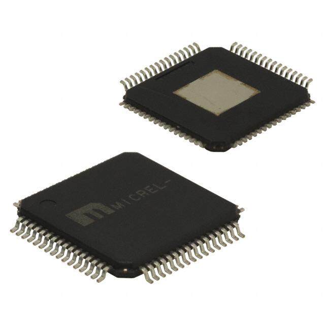
| 描述 | TXRX USB 2.0 ULPI 36-TFBGAUSB 接口集成电路 USB 2.0 ULPI Xcvr |
| 产品分类 | |
| 品牌 | Texas Instruments |
| 产品手册 | |
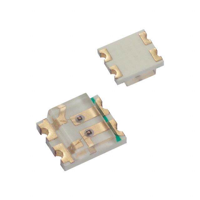
| 产品图片 |
|
| rohs | 符合RoHS无铅 / 符合限制有害物质指令(RoHS)规范要求 |
| 产品系列 | 接口 IC,USB 接口集成电路,Texas Instruments TUSB1211A1ZRQR- |
| 数据手册 | |
| 产品型号 | TUSB1211A1ZRQR |
| 产品种类 | USB 接口集成电路 |
| 供应商器件封装 | 36-BGA MircoStar Junior |
| 其它名称 | 296-28357-1 |
| 包装 | 剪切带 (CT) |
| 协议 | USB 2.0 |
| 双工 | - |
| 商标 | Texas Instruments |
| 安装类型 | 表面贴装 |
| 安装风格 | SMD/SMT |
| 封装 | Reel |
| 封装/外壳 | 36-VFBGA |
| 封装/箱体 | BGA-36 Microstar Junior |
| 工作温度 | -40°C ~ 85°C |
| 工作电源电压 | 3.6 V |
| 工厂包装数量 | 1500 |
| 接收器滞后 | - |
| 数据速率 | - |
| 最大工作温度 | + 85 C |
| 最小工作温度 | - 40 C |
| 标准 | USB 2.0 |
| 标准包装 | 1 |
| 电压-电源 | 2.7 V ~ 4.8 V |
| 类型 | 收发器 |
| 系列 | TUSB1211 |
| 速度 | High-Speed |
| 驱动器/接收器数 | 8/8 |


- 商务部:美国ITC正式对集成电路等产品启动337调查
- 曝三星4nm工艺存在良率问题 高通将骁龙8 Gen1或转产台积电
- 太阳诱电将投资9.5亿元在常州建新厂生产MLCC 预计2023年完工
- 英特尔发布欧洲新工厂建设计划 深化IDM 2.0 战略
- 台积电先进制程称霸业界 有大客户加持明年业绩稳了
- 达到5530亿美元!SIA预计今年全球半导体销售额将创下新高
- 英特尔拟将自动驾驶子公司Mobileye上市 估值或超500亿美元
- 三星加码芯片和SET,合并消费电子和移动部门,撤换高东真等 CEO
- 三星电子宣布重大人事变动 还合并消费电子和移动部门
- 海关总署:前11个月进口集成电路产品价值2.52万亿元 增长14.8%


PDF Datasheet 数据手册内容提取
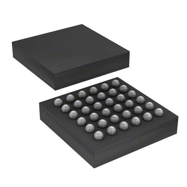
Product Sample & Technical Tools & Support & Folder Buy Documents Software Community TUSB1211 SLLSE80B–MARCH2011–REVISEDJUNE2015 TUSB1211 Stand-Alone USB Transceiver Chip 1 Device Overview 1.1 Features 1 • USB2.0PHYTransceiverChip,Designedto • USBHSStart-of-FrameClockOutputFeature InterfaceWithaUSBControllerThroughaULPI AvailableonSOFPinCanbeUsedtoSynchronize Interface,FullyCompliantWith: AnotherApplication,forExampleAudio,Withthe – UniversalSerialBusSpecificationRev.2.0 USBPacketStream – On-The-GoSupplementtotheUSB2.0 • ULPIInterface: SpecificationRev.1.3 – I/OInterface(1.8V)OptimizedforNon- – UTMI+LowPinInterface(ULPI)Specification Terminated50-Ω LineImpedance Rev.1.1 – ULPICLOCKPin(60MHz)SupportsBothInput • DP/DMLineExternalComponentCompensation andOutputClockConfigurations (Patent#US7965100B1) – FullyProgrammableULPI-CompliantRegister • InterfacestoHost,Peripheral,andOTGDevice Set Cores;OptimizedforPortableDevicesorSystem • FullIndustrial-GradeOperatingTemperature ASICsWithBuilt-inUSBOTGDeviceCore Rangefrom–40°Cto85°C • CompleteUSBOTGPhysicalFront-End • AvailableinaTFBGA36BallPackage • USBBatteryChargerDetectionFeature 1.2 Applications • MobilePhones • VideoGameConsoles • PortableComputers • DesktopComputers • TabletDevices • PortableMusicPayers 1.3 Description The TUSB1211 device is a USB2.0 transceiver chip, designed to interface with a USB controller through a ULPI interface. The device supports all USB2.0 data rates (high-speed 480 Mbps, full-speed 12 Mbps and low-speed 1.5 Mbps), and is compliant to both Host and Peripheral modes. The TUSB1211 also supports aUARTmodeandlegacyULPIserialmodes. The TUSB1211 device supports the OTG (Ver1.3) optional addendum to the USB 2.0 Specification, includingHostNegotiationProtocol(HNP)andSessionRequestProtocol(SRP).TUSB1211alsosupports USB Battery Charging Specification Ver1.1 integrating a charger detection module for sensing and control onDP/DMlines,andACA(AccessoryChargerAdapter)detectionandcontrolonIDline. The DP/DM external component compensation in the transmitter compensates for variations in the series impendence to match with the data line impedance and the receiver input impedance, to limit data reflectionsand,thereby,improveeyediagrams. DeviceInformation(1) PARTNUMBER PACKAGE BODYSIZE(NOM) TUSB1211 BGAMICROSTARJUNIOR(36) 3.50mm×3.50mm (1) Forallavailablepackages,seetheorderableaddendumattheendofthedatasheet. 1 AnIMPORTANTNOTICEattheendofthisdatasheetaddressesavailability,warranty,changes,useinsafety-criticalapplications, intellectualpropertymattersandotherimportantdisclaimers.PRODUCTIONDATA.
TUSB1211 SLLSE80B–MARCH2011–REVISEDJUNE2015 www.ti.com 1.4 Functional Block Diagram 2 DeviceOverview Copyright©2011–2015,TexasInstrumentsIncorporated SubmitDocumentationFeedback ProductFolderLinks:TUSB1211
TUSB1211 www.ti.com SLLSE80B–MARCH2011–REVISEDJUNE2015 Table of Contents 1 DeviceOverview......................................... 1 4.23 HSTransmitter...................................... 16 .............................................. ...................... 1.1 Features 1 4.24 PullupandPulldownResistors 17 ........................................... ....................... 1.2 Applications 1 4.25 AutoresumeWatchdogTimer 17 ............................................ .................................. 1.3 Description 1 4.26 UARTTransceiver 17 ............................ ................................... 1.4 FunctionalBlockDiagram 2 4.27 OTGIDElectrical 17 2 Revision History......................................... 4 4.28 ElectricalSpecs–ChargerDetectionCurrents..... 19 3 PinConfigurationandFunctions..................... 5 4.29 ElectricalSpecs–Resistance ...................... 19 .......................................... ..................... 3.1 PinDiagram 5 4.30 ElectricalSpecs–Capacitance 19 4 Specifications ............................................ 8 4.31 ChargerDetectionDebounceandWaitTiming..... 19 .......................... ....................................... 4.1 AbsoluteMaximumRatings 8 4.32 ULPIInterface 20 .......................................... ......................... 4.2 ESDRatings 8 4.33 Power-OnTimingDiagrams 20 ................ ........................................ 4.3 RecommendedOperatingConditions 8 4.34 ClockSystem 23 ....................... ........................................ 4.4 PowerConsumptionSummary 9 4.35 ClockSystem 23 ...... ................................. 4.5 ElectricalCharacteristics–AnalogOutputPins 9 4.36 PowerManagement 23 ...... ...................................... 4.6 ElectricalCharacteristics–AnalogInputPins 10 4.37 PowerProvider 24 4.7 DigitalI/OElectricalCharacteristics–Non-ULPI 4.38 PowerControl....................................... 25 .................................................. Pins 10 5 DetailedDescription................................... 26 4.8 DigitalI/OElectricalCharacteristics–Non-ULPI ............................................ .................................................. 5.1 Overview 26 Pins 10 .......................... ................ 5.2 FunctionalBlockDiagram 26 4.9 ElectricalCharacteristics–REFCLK 10 ................................. ........... 5.3 FeatureDescription 26 4.10 ElectricalCharacteristics–CLOCKInput 11 ....................................... ................ 5.4 RegisterMaps 32 4.11 ElectricalCharacteristics–REFCLK 11 6 Application,Implementation,andLayout......... 70 4.12 ElectricalCharacteristics–CK32KClock Generator............................................ 11 6.1 ApplicationInformation.............................. 70 4.13 Thermal Characteristics............................. 11 6.2 TypicalApplication.................................. 70 4.14 REG3V3InternalLDORegulatorCharacteristics... 12 6.3 Layout............................................... 72 4.15 REG1V8InternalLDORegulatorCharacteristics... 12 6.4 PowerSupplyRecommendations................... 73 4.16 REG1V5InternalLDORegulatorCharacteristics... 12 7 DeviceandDocumentationSupport............... 74 4.17 TimersandDebounce .............................. 13 7.1 DocumentationSupport............................. 74 4.18 OTGVBUSElectrical............................... 14 7.2 Trademarks.......................................... 74 4.19 LS/FSSingle-EndedReceivers..................... 15 7.3 ElectrostaticDischargeCaution..................... 74 4.20 LS/FSDifferentialReceiver......................... 15 7.4 Glossary............................................. 74 4.21 LS Transmitter...................................... 15 8 MechanicalPackagingandOrderable ...................................... Information.............................................. 74 4.22 FS Transmitter 15 .............................. 8.1 PackagingInformation 74 Copyright©2011–2015,TexasInstrumentsIncorporated TableofContents 3 SubmitDocumentationFeedback ProductFolderLinks:TUSB1211
TUSB1211 SLLSE80B–MARCH2011–REVISEDJUNE2015 www.ti.com 2 Revision History NOTE:Pagenumbersforpreviousrevisionsmaydifferfrompagenumbersinthecurrentversion. ChangesfromRevisionA(January2012)toRevisionB Page • Deletedsomeofthefeaturesperthesubmittedsources....................................................................... 1 • ChangedthedocumenttothenewTIstandardlayout ......................................................................... 1 • ChangedpinF5fromAtoDintheA/Dcolumn ................................................................................. 6 • AddedtheAnalogOutputPinssection............................................................................................ 9 • AddedthewordNontothetileNon-ULPIPinsandreplacedtheDigitalI/OElectricalCharacteristics–Non-ULPI Pinstabledata....................................................................................................................... 10 • AddedtheTimersandDebouncesection........................................................................................ 13 • AddedtheOTGVBUSSpecifications............................................................................................ 14 • AddedthePullupandPulldownResistorstable................................................................................ 17 • AddedSection4.26 ................................................................................................................ 17 • AddedtheOTGIDElectricaltable................................................................................................ 17 • AddedtheULPIInterfacesection................................................................................................. 20 • AddedthePower-OnTimingDiagramssection................................................................................. 20 • AddedtheInternalClockGenerator(32kHz)................................................................................... 23 • AddedthePowerProvidersection ............................................................................................... 24 • ChangedthelocationofparagraphsfromDescriptiontoDetailedDescription,subsectionOverview................... 26 • AddedtheLS/FSSingle-EndedReceiverssection............................................................................. 28 • AddedtheLS/FSDifferentialReceiversection.................................................................................. 28 • AddedtheLS/FSTransmitter...................................................................................................... 28 • AddedtheHSDifferentialReceiversection..................................................................................... 28 • AddedtheHSDifferentialTransmittersection.................................................................................. 29 • AddedtheAutoresumesection.................................................................................................... 29 • AddedtheRegisterMapsection ................................................................................................. 32 • AddedtheApplicationandImplementationsection ............................................................................ 70 • DeletedtwoListItemsfromtheUnusedPinsConnectionsection........................................................... 71 • AddedtheLayoutsection.......................................................................................................... 72 • AddedthePowerSupplyRecommendationssection.......................................................................... 73 4 RevisionHistory Copyright©2011–2015,TexasInstrumentsIncorporated SubmitDocumentationFeedback ProductFolderLinks:TUSB1211
TUSB1211 www.ti.com SLLSE80B–MARCH2011–REVISEDJUNE2015 3 Pin Configuration and Functions 3.1 Pin Diagram ZRQPackage 36-PinTFBGA BottomView TFBGA36 PACKAGE (BOTTOMVIEW) CHRG_ CHRG_ F VBAT VBUS REFCLK SOF POL DET CHRG_ E FAULT REG3V3 GND DIR REG1V5 EN_N D DP GND ID PSW NXT STP C DM NC(1) CS_N RESET_N GND DATA7 B DATA0 VDDIO CS CFG VDDIO DATA6 A DATA1 DATA2 DATA3 CLOCK DATA4 DATA5 1 2 3 4 5 6 (1) NC=NotConnected (2) Thesizeofthedeviceshouldbe3.5mm±0.1mmby3.5mm±0.1mm.Heightis1.0mmtypical1.15mmmaxincludingthesolder balls.Thepitchofthedeviceis0.5mm.Ballwidth0.3mm±0.05mm. 3.1.1 Pin Attributes PinFunctions NO. PIN(1) NAME A/D(2) TYPE(3) LEVEL(4) DESCRIPTION 1 D5 NXT D O V ULPINXToutputsignal DDIO 2 B1 DATA0 D I/O V ULPIDATAinput/outputsignalsynchronizedtoCLOCK DDIO 3 A1 DATA1 D I/O V ULPIDATAinput/outputsignalsynchronizedtoCLOCK DDIO 4 A2 DATA2 D I/O V ULPIDATAinput/outputsignalsynchronizedtoCLOCK DDIO 5 A3 DATA3 D I/O V ULPIDATAinput/outputsignalsynchronizedtoCLOCK DDIO 6 A5 DATA4 D I/O V ULPIDATAinput/outputsignalsynchronizedtoCLOCK DDIO 7 A6 DATA5 D I/O V ULPIDATAinput/outputsignalsynchronizedtoCLOCK DDIO 8 B6 DATA6 D I/O V ULPIDATAinput/outputsignalsynchronizedtoCLOCK DDIO Active-highchipselectpin.WhenlowtheICisinpowerdown 9 B3 CS D I V andULPIbusistri-stated.Whenhigh(andCS_NpiniTieto DDIO VDDIOifunused.slow)normaloperation. 1.5VinternalLDOoutput.Connecttoexternalfiltering 10 E6 REG1V5 A POWER V DD15 capacitor. 11 C6 DATA7 D I/O V ULPIDATAinput/outputsignalsynchronizedtoCLOCK DDIO (1) Pin=PackagePincoordinateof (2) A/D:A=Analogpin,D=Digitalpin (3) TYPE:I=Inputpintype,O=Outputpintype,I/O=Input/Outputpintype,POWER=Powersupplypintype, GROUND=Groundtypepin (4) LEVEL=Pinpowersupplylevel Copyright©2011–2015,TexasInstrumentsIncorporated PinConfigurationandFunctions 5 SubmitDocumentationFeedback ProductFolderLinks:TUSB1211
TUSB1211 SLLSE80B–MARCH2011–REVISEDJUNE2015 www.ti.com PinFunctions(continued) NO. PIN(1) NAME A/D(2) TYPE(3) LEVEL(4) DESCRIPTION REFCLKclockfrequencyconfigurationpin. 12 B4 CFG D I V Twofrequenciesaresupported:19.2MHzwhen0,or26MHz DDIO when1. 13 D1 DP A I/O V DPpinoftheUSBconnector DD33 14 C1 DM A I/O V DMpinoftheUSBconnector DD33 3.3VinternalLDOoutput.Connecttoexternalfiltering 15 E3 REG3V3 A POWER V DD33 capacitor. 16 F3 VBAT A POWER V Inputsupplyvoltageorbatterysource.Nominally3.3Vto4.5V BAT 17 F4 VBUS A I/O V VBUSpinoftheUSBconnector BUS 18 D3 ID A I/O V Identification(ID)pinoftheUSBconnector BUS ULPI60-MHzclockonwhichULPIdataissynchronized.2 modesarepossible: InputMode:CLOCKdefaultsasaninput(thisisthedefault 19 A4 CLOCK D I/O V DDIO clockmode) OutputMode:WhenaninputclockisdetectedonREFCLKpin thenCLOCKwillchangetoanoutput Activelowchipresetpin.Minimumpulsewidth100µs.When lowalldigitallogic(except32-kHzlogicrequiredforpower-up sequencingandchargerdetectionstate-machine)including 20 C4 RESET_N D I V DDIO registersareresettotheirdefaultvalues.ULPIbusisin“ULPI Synchronousmodepower-upPLLOFF”stateasdescribedin Table5-5.WhenhighnormalUSBoperation. 21 D6 STP D I V ULPISTPinputsignal DDIO 22 E5 DIR D O V ULPIDIRoutputsignal DDIO External1.8-VsupplyinputfordigitalI/Os.Connecttoexternal 23 B5 VDDIO A I V DDIO filteringcapacitor. External1.8-VsupplyinputfordigitalI/Os.Connecttoexternal 24 B2 VDDIO A I V DDIO filteringcapacitor. 25 C5 GND A GROUND GND Ground 26 D2 GND A GROUND GND Ground 27 E4 GND A GROUND GND Ground Referenceclockinput. InputreferenceclockfrequencymustbeindicatedbyCFGpin. 28 F5 REFCLK D I V DDIO Twofrequenciesaresupported:19.2MHz(whenCFG=0),and 26MHz(whenCFG=1). HSUSBSOF(Start-of-Frame)outputclock.(featurecontrolled 29 F6 SOF D O V bySOF_ENbit,disabledandoutputlogiclowbydefault.).HS DDIO USBSOFpacketrateis8kHz. 30 C2 NC — — Notconnected Active-lowchipselectpin.WhenhightheICisinpowerdown 31 C3 CS_N D I V andULPIbusistri-stated.Whenlow(andCSpinishigh) DDIO normaloperation.TietoGNDifunused. ActivelowinputpinusedtoenableBatteryChargingDetection inDeadBatteryChargerDetectionmode.Thispinisignoredin 32 E1 CHRG_EN_N D I V BAT ACTIVEmode.ConnecttoGNDtoactivate.ConnecttoVBAT whenchargerdetectionnotrequired. VBUSfaultdetectorinputusedas EXTERNALVBUSINDICATORinTUSB1211.Thelinkmust enableVBUSfaultdetectionthroughthe USEEXTERNALVBUSINDICATORregisterbit,andthepolarity 33 E2 FAULT D I V BAT mustbesetthroughtheINDICATORCOMPLEMENTregister bit.INDICATORPASSTHRUbitcanbeusedtoqualifyFAULT withtheinternalvbusvalidcomparator.ConnecttoGNDifnot used.Thispinis5-Vtolerant. WhenconnectedtoGNDthenCHRG_DEToutputpinisactive 34 F1 CHRG_POL D I V low.WhenconnectedtoVBATthenCHRG_DEToutputpinis BAT activehigh. 6 PinConfigurationandFunctions Copyright©2011–2015,TexasInstrumentsIncorporated SubmitDocumentationFeedback ProductFolderLinks:TUSB1211
TUSB1211 www.ti.com SLLSE80B–MARCH2011–REVISEDJUNE2015 PinFunctions(continued) NO. PIN(1) NAME A/D(2) TYPE(3) LEVEL(4) DESCRIPTION WhenCHRG_POLpinisatGNDthenCHRG_DETisinactive lowopen-drainmodewithexternalRCHRGDET(100K) 35 F2 CHRG_DET D O V connectedtoVBAT.WhenCHRG_POLpinisatVBATthen BAT CHRG_DETisinactivehighopen-sourcemodewithexternal RCHRGDET(100K)connectedtoGND.Thispinis5-Vtolerant. Controlsanexternal,activehigh,VBUSpowerswitchorcharge pump.OpensourceoutputonVBATsupplywhenPSW_OSOD 36 D4 PSW D O V bitis0(default),open-drainactive-lowoutputwhen BAT PSW_OSODbitis1.RequiresanexternalRPSW(100K) pulldown/pullupresistortoGND/VBAT. Copyright©2011–2015,TexasInstrumentsIncorporated PinConfigurationandFunctions 7 SubmitDocumentationFeedback ProductFolderLinks:TUSB1211
TUSB1211 SLLSE80B–MARCH2011–REVISEDJUNE2015 www.ti.com 4 Specifications 4.1 Absolute Maximum Ratings overoperatingfree-airtemperaturerange(unlessotherwisenoted)(1) MIN MAX UNIT Mainbatterysupplyvoltage Continuous 0 5.0 V Theproductwillhavenegligiblereliability VBAT(2) impactforpulsedvoltagespikesof5.5Vfora Mainbatterysupplyvoltagepulsed 5.5 V total(cumulativeoverlifetime)durationof5 milliseconds V IOsupplyvoltage Continuous 1.98 V DDIO WhereV representsthevoltageappliedto VoltageonanyinputexceptV , DD DDIO thepowersupplypinassociatedwiththe –0.3 1.0×V +0.3 V V ,andV pads DD BAT BUS input DPorDMorIDpinsshort-circuitedtoVBUS DP,DM,IDhighvoltageshortcircuit supply,inanymodeofTUSB1211operation, 5.25 V continuouslyfor24hours DPorDMorIDpinsshort-circuitedtoGNDin DP,DM,IDlowvoltageshortcircuit anymodeofTUSB1211operation, 0 V continuouslyfor24hours V input(3) –2 20 V BUS T Ambienttemperature –40 85 °C A T Junctiontemperature –40 150 °C J T Storagetemperature –55 125 °C stg (1) StressesbeyondthoselistedunderAbsoluteMaximumRatingsmaycausepermanentdamagetothedevice.Thesearestressratings only,andfunctionaloperationofthedeviceattheseoranyotherconditionsbeyondthoseindicatedunderSection4.3isnotimplied. Exposuretoabsolute-maximum-ratedconditionsforextendedperiodsmayaffectdevicereliability. (2) IfVBATexceedsaboveratingadevicetodropdownthevoltagebeforeappliedtothedevice. (3) IfVBUSexceedsaboveratinganexternalvoltageprotectiononthelineismandatorybetweentheVBUSlineandtheTUSB1211. 4.2 ESD Ratings VALUE UNIT Humanbodymodel(HBM),perANSI/ESDA/JEDECJS-001(1) ±2000 V Electrostaticdischarge V (ESD) Charged-devicemodel(CDM),perJEDECspecificationJESD22-C101(2) ±500 (1) JEDECdocumentJEP155statesthat500-VHBMallowssafemanufacturingwithastandardESDcontrolprocess. (2) JEDECdocumentJEP157statesthat250-VCDMallowssafemanufacturingwithastandardESDcontrolprocess. 4.3 Recommended Operating Conditions overoperatingfree-airtemperaturerange(unlessotherwisenoted) MIN TYP MAX UNIT V Batterysupplyvoltage VBAT_ACTIVE 2.7 3.6 4.8 V BAT WhenV issuppliedinternally 3.15 DD33 BatterysupplyvoltageforUSB2.0compliancy VBAT_CERT (USB2.0certification) WhenVDD33isshortedtoVBAT 3.05 V externally Batterysupplyvoltageforchargerdetectin 2.4 V VBAT_DB V BAT_DB “dead-batterycondition” V IOsupplyvoltage VDDIO_ACTIVE 1.62 1.8 1.95 V DDIO T Ambienttemperaturerange –40 85 °C A T Junctiontemperature Forparametriccompliance –40 125 °C J 8 Specifications Copyright©2011–2015,TexasInstrumentsIncorporated SubmitDocumentationFeedback ProductFolderLinks:TUSB1211
TUSB1211 www.ti.com SLLSE80B–MARCH2011–REVISEDJUNE2015 4.4 Power Consumption Summary(1)(2) TYPICALPOWER MODE CONDITIONS SUPPLY UNIT CONSUMPTION IV 8 BAT V =3.6V,V =1.8V, OFF BAT DDIO IV 1.8 µA CS=0V DDIO I 9.8 TOTAL IV 251 V =5V,V =3.6V, BAT BUS BAT Suspend V =1.8V,VCHRG_EN_N=0V, IV 21 µA DDIO DDIO noclock I 272 TOTAL IV 46.4 BAT V =3.6V,V =1.8V, HSUSBMode BAT DDIO IV 1.3 mA activeUSBtransfer DDIO I 47.7 TOTAL IV 31.4 BAT V =3.6V,V =1.8V, FSUSBMode BAT DDIO IV 1.3 mA activeUSBtransfer DDIO I 32.7 TOTAL (1) Describesthepowerconsumptiondependingontheusecases. (2) TypicalpowerconsumptionisobtainedinnominaloperatingconditionsoftheTUSB1211device. 4.5 Electrical Characteristics – Analog Output Pins PARAMETER TESTCONDITIONS MIN TYP MAX UNIT CHRG_DETOUTPUTPIN CHRG_DETexternalpullup WhenCHRG_POLpin=GND,thatis,inopen- R 60 100 kΩ CDETPUOD resistortoVBAT drainmode(active-low) CHRG_DETminimumhigh-level WhenCHRG_POLpin=GND,thatis,inopen- 0.7× VOH V CDETOD outputvoltage drainmode(active-low) V BAT CHRG_DETmaximumcurrent WhenCHRG_POLpin=GND,thatis,inopen- IOH 2 mA CDETOD fromVBAT drainmode(active-low) CHRG_DETexternalpulldown WhenCHRG_POLpin=VBAT,thatis,inopen- R 60 100 kΩ CDETPDOS resistortoGND sourcemode(active-high) CHRG_DETmaximumlow-level WhenCHRG_POLpin=VBAT,thatis,inopen- 0.3× VOL V CDETOS outputvoltage sourcemode(active-high) V BAT CHRG_DETminimumcurrent WhenCHRG_POLpin=VBAT,thatis,inopen- IOH –2 mA CDETOS fromVBAT sourcemode(active-high) PSWOUTPUTPIN PSWexternalpullupresistorto R Whenconfiguredinopen-drainactivelowmode 60 100 kΩ PSWPUOD VBAT PSWminimumhigh-leveloutput Whenconfiguredinopen-drainactivelowmodeor 0.7× VOH V PSW voltage CMOSmode V BAT PSWmaximumcurrentfrom IOH Whenconfiguredinopen-drainactivelowmode 2 mA PSWOD VBAT PSWexternalpulldownresistor Whenconfiguredinopen-sourceactivehighmode R 60 100 kΩ PSWPDOS toground (default) PSWminimumhigh-leveloutput Whenconfiguredinopen-sourceactivehighmode 0.3× VOL V PSW voltage (default)orCMOSmode V BAT PSWmaximumcurrentfrom Whenconfiguredinopen-sourceactivehighmode IOH –2 mA PSWOS VBAT (default) Copyright©2011–2015,TexasInstrumentsIncorporated Specifications 9 SubmitDocumentationFeedback ProductFolderLinks:TUSB1211
TUSB1211 SLLSE80B–MARCH2011–REVISEDJUNE2015 www.ti.com 4.6 Electrical Characteristics – Analog Input Pins PARAMETER TESTCONDITIONS MIN TYP MAX UNIT CHRG_EN_NINPUTPIN VILCDETENN CHRG_EN_Nmaximumlow-levelinputvoltage 0.3 V VIHCDETENN CHRG_EN_Nminimumhigh-levelinputvoltage 1.0 V CHRG_POLINPUTPIN VILCHRG_POL CHRG_POLmaximumlow-levelinputvoltage 0.3 V VIHCHRG_POL CHRG_POLminimumhigh-levelinputvoltage 1.0 V FAULTINPUTPIN VILFAULT FAULTmaximumlow-levelinputvoltage 0.3 V VIHFAULT FAULTminimumhigh-levelinputvoltage 1.0 V 4.7 Digital I/O Electrical Characteristics – Non-ULPI Pins overoperatingfree-airtemperaturerange(unlessotherwisenoted) PARAMETER TESTCONDITIONS MIN TYP MAX UNIT CLOCK V Low-levelinputvoltage 0.4 V OL Frequency=60MHz,Load=10pF V High-levelinputvoltage V –0.45 V OH DDIO STP,DIR,NXT,DATA0toDATA7 V Low-levelinputvoltage 0.45 V OL Frequency=360MHz,Load=10pF V High-levelinputvoltage V –0.45 V OH DDIO 4.8 Digital I/O Electrical Characteristics – Non-ULPI Pins PARAMETER TESTCONDITIONS MIN TYP MAX UNIT CS,CFG,RESETBINPUTPINS V Maximumlow-levelinputvoltage 0.35×V V IL DDIO V Minimumhigh-levelinputvoltage 0.65×V V IH DDIO RESET_NINPUTPINTIMINGSPECIFICATION t Internalpower-onresetpulsewidth 0.2 µs w(POR) AppliedtoexternalRESET_Npinwhen CLOCK t ExternalRESET_Npulsewidth 8 w(RESET) CLOCKistoggling. cycles 4.9 Electrical Characteristics – REFCLK PARAMETER TESTCONDITIONS MIN(1) TYP MAX(1) UNIT V Lowlevelinputvoltage 0.35×V V IL DDIO V Highlevelinputvoltage 0.65×V V IH DDIO (1) V voltagelevel=1.8V DDIO 10 Specifications Copyright©2011–2015,TexasInstrumentsIncorporated SubmitDocumentationFeedback ProductFolderLinks:TUSB1211
TUSB1211 www.ti.com SLLSE80B–MARCH2011–REVISEDJUNE2015 4.10 Electrical Characteristics – CLOCK Input overoperatingfree-airtemperaturerange(unlessotherwisenoted) PARAMETER TESTCONDITIONS MIN TYP MAX UNIT CLOCKinputdutycycle 40% 60% F CLOCKnominalfrequency 60 MHz CLOCK CLOCKinputrise/falltime In%ofCLOCKperiodT (=1/F ) 10% CLOCK CLOCK CLOCKinputfrequencyaccuracy 250 ppm CLOCKinputintegratedjitter 600 psrms 4.11 Electrical Characteristics – REFCLK overoperatingfree-airtemperaturerange(unlessotherwisenoted) PARAMETER TESTCONDITIONS MIN TYP MAX UNIT REFCLKinputdutycycle 40% 60% WhenCFGpinistiedtoGND 19.2 FREFCLKREFCLKnominalfrequency MHz WhenCFGpinistiedtoV 26 DDIO REFCLKinputrise/falltime In%ofREFCLKperiodT (=1/F ) 20% REFCLK REFCLK REFCLKinputfreqaccuracy 250 ppm REFCLKinputintegratedjitter 600 psrms 4.12 Electrical Characteristics – CK32K Clock Generator overoperatingfree-airtemperaturerange(unlessotherwisenoted) PARAMETER TESTCONDITIONS MIN TYP MAX UNIT Outputdutycycle 48% 50% 52% Outputfrequency 23 32.7 38 kHz 4.13 Thermal Characteristics THERMALMETRIC(1) TUSB1211 ZRQ(BGAMICROSTARJUNIOR) UNIT 36PINS R Junction-to-ambientthermalresistance(2) 69.2 °C/W θJA R Junction-to-case(top)thermalresistance(3)(4) 41 °C/W θJC(top) R Junction-to-case(bottom)thermalresistance(4)(5) N/A °C/W θJC(bot) Junction-to-board thermalresistanceorjunction-to-pinthermal RθJB resistance(6) 42 °C/W Ψ Junction-to-topofpackage(notatruethermalresistance)(7) 0.9 °C/W JT Ψ Junction-to-board(notatruethermalresistance)(8) 71 °C/W JB (1) Formoreinformationabouttraditionalandnewthermalmetrics,seetheapplicationreport,SemiconductorandICPackageThermal Metrics(SPRA953). (2) Measurementmethod:EIA/JESD51-1 (3) TopissurfaceofthepackagefacingawayfromthePCB. (4) NocurrentJEDECspecification(seetheapplicationreport,SemiconductorandICPackageThermalMetrics(SPRA953). (5) BottomsurfaceisthesurfaceofthepackagefacingtowardsthePCB. (6) Measurementmethod:EIA/JESD51-8 (7) Measurementmethod:EIA/JESD51-2 (8) Measurementmethod:EIA/JESD51-6 Copyright©2011–2015,TexasInstrumentsIncorporated Specifications 11 SubmitDocumentationFeedback ProductFolderLinks:TUSB1211
TUSB1211 SLLSE80B–MARCH2011–REVISEDJUNE2015 www.ti.com 4.14 REG3V3 Internal LDO Regulator Characteristics overoperatingfree-airtemperaturerange(unlessotherwisenoted) PARAMETER TESTCONDITIONS MIN TYP MAX UNIT V Inputvoltage V V +0.15 3.6 4.8 V INREG3V3 BAT OUT(typ) Onmode–REG3V3_VSEL<2:0>=‘000 2.4 2.5 2.6 Onmode–REG3V3_VSEL<2:0>=‘001 2.65 2.75 2.85 Onmode–REG3V3_VSEL<2:0>=‘010 2.9 3. 3.1 Onmode–REG3V3_VSEL<2:0>=‘011 VV Outputvoltage (default) 3 3.1 3.2 V DD33 ACTIVEmode Onmode–REG3V3_VSEL<2:0>=‘100 3.1 3.2 3.3 Onmode–REG3V3_VSEL<2:0>=‘101 3.2 3.3 3.4 Onmode–REG3V3_VSEL<2:0>=‘110 3.3 3.4 3.5 Onmode–REG3V3_VSEL<2:0>=‘111 3.4 3.5 3.6 Outputvoltage V <V <3.1V V –0.05 V V BAT_DB BAT BAT BAT BAT+0.05 hardwarecharger VV V DD33_DB detection V >3.1V 3 3.1 3.2 BAT (deadbattery)mode V :ACTIVEmode, BAT I Ratedoutputcurrent Hardwarechargerdetection(deadbattery) 15 mA REG3V3 mode Ratedoutputcurrent: I Suspendmode/resetmode 1 mA REG3V3_SUSP IREG3V3_SUSP 4.15 REG1V8 Internal LDO Regulator Characteristics overoperatingfree-airtemperaturerange(unlessotherwisenoted) PARAMETER TESTCONDITIONS MIN TYP MAX UNIT V Inputvoltage Onmode:V =V 2.4 3.6 4.8 V INREG1V8 INREG1V8 BAT V Outputvoltage 1.75 1.87 1.98 V REG1V8 I Ratedoutputcurrent Onmode 30 mA REG1V8 4.16 REG1V5 Internal LDO Regulator Characteristics overoperatingfree-airtemperaturerange(unlessotherwisenoted) PARAMETER TESTCONDITIONS MIN TYP MAX UNIT V Inputvoltage Onmode:V =V 2.4 3.6 4.8 V INREG1V8 INREG1V8 BAT V Outputvoltage 1.45 1.56 1.65 V REG1V8 I Ratedoutputcurrent Onmode 50 mA REG1V8 12 Specifications Copyright©2011–2015,TexasInstrumentsIncorporated SubmitDocumentationFeedback ProductFolderLinks:TUSB1211
TUSB1211 www.ti.com SLLSE80B–MARCH2011–REVISEDJUNE2015 4.17 Timers and Debounce overoperatingfree-airtemperaturerange(unlessotherwisenoted) NBCK32K TEST PARAMETER MIN TYP MAX UNIT CYCLES CONDITIONS TDEL_CS_SUPPLYOK Chip-select-to-Suppliesokdelay N/A 4.19 ms ResetbtoPHYPLLlockedandDIR TDEL_RST_DIR N/A 0.42 ms falling-edgedelay TVBAT_DET VBATdetectiondelay N/A 10.0 µs TBGAP Bandgappower-ondelay N/A 2.0 ms TPWONREG1V5 REG1V5power-ondelay N/A 100.0 µs TPWONREG1V8 REG1V8power-ondelay N/A 100.0 µs TPWONVREG3V3 REG3V3power-ondelay N/A 1.0 ms TPWONCK32K 32KHzRC-OSCpower-ondelay N/A 125.0 µs TDELRSTPWR Powercontrolresetdelay 2 52.6 61.0 87.0 µs TDELMNTRVIOEN Monitorenabledelay 3 78.9 91.6 130.4 µs TMNTR Supplymonitoringdebounce 6 157.9 183.1 260.9 µs TDELREG3V3EN REG3V3LDOenabledelay 3 78.9 91.6 130.4 µs TDELRESET_N RESET_Ninternaldelay 4 105.3 122.1 173.9 µs TPLL PLLLocktime N/A 300.0 µs Min4100 TERROR_DELAY PWRFSMERRORstatedelay 107.9 125.1 356.3 ms Max8196 Copyright©2011–2015,TexasInstrumentsIncorporated Specifications 13 SubmitDocumentationFeedback ProductFolderLinks:TUSB1211
TUSB1211 SLLSE80B–MARCH2011–REVISEDJUNE2015 www.ti.com 4.18 OTG VBUS Electrical overoperatingfree-airtemperaturerange(unlessotherwisenoted) PARAMETER TESTCONDITIONS MIN TYP MAX UNIT V COMPARATORS BUS RVBUS=0ΩandR1KSERIES=0 4.4 4.5 4.625 RVBUS=1000Ω±10%and 4.4 4.5 4.625 R1KSERIES=1 VA_VBUS_VLD A-deviceVBUSvalid RVBUS=1200Ω±10%and V 4.4 4.5 4.625 R1KSERIES=1 RVBUS=1800Ω±10%and 4.4 4.5 4.675 R1KSERIES=1 V A-devicesessionvalid 0.8 1.4 2.0 V SESS_VLD V B-devicesessionvalid 2.1 2.4 2.7 V B_SESS_VLD V B-devicesessionend 0.2 0.5 0.8 V B_SESS_END V LINE BUS SRP(V pulsing)capableA-devicenotdriving BUS V , A-deviceV input BUS R BUS ForV <V ,(WhenbitR 40 100 kΩ VBUS_IDLE_A impedancetoground BUS SESS_VLD ABUSIN_EN=1 /R impedance RVBUS_IDLE_A VUS_IDLE_A_HI_RANGE controlledautomaticallybyhardware) SRP(V pulsing)capableA-devicenotdriving BUS V A-deviceV input BUS BUS ForV >V R impedancetoground(for BUS SESS_VLD 70 100 kΩ VUS_IDLE_A_HI_RANGE (WhenbitR / V hi-range) ABUSIN_EN=1RVBUS_IDLE_A BUS R impedancecontrolled VUS_IDLE_A_HI_RANGE automaticallybyhardware) WhenbitR =0 B-deviceV input ABUSIN_EN R BUS ForV inrange[0V:20V] 150 220 400 kΩ VBUS_IDLE_B impedancetoground BUS (NotvalidfornegativevaluesofV ) BUS B-deviceV SRP R BUS 5 10 20 kΩ B_SRP_DWN pulldown R B-deviceV SRPpullup 0.85 1.3 1.75 kΩ B_SRP_UP BUS RV =0Ωand BUS 31.4 R1KSERIES=0 RV =1000Ω±10%and B-deviceVBUSSRPrise 0to2.1V R1KBUSSERIES=1 57.8 t timemaximumforOTG-A with<13μF ms RISE_SRP_UP_MAX communication load, RVBUS=1200Ω±10%and 64 R1KSERIES=1 RV =1800Ω±10%and BUS 85.4 R1KSERIES=1 RV =0Ωand BUS 46.2 R1KSERIES=0 RV =1000Ω±10%and B-deviceVBUSSRPrise 0.8to2.0V R1KBUSSERIES=1 96 t timeminimumfor with>97μF ms RISE_SRP_UP_MIN standardhostconnection load, RVBUS=1200Ω±10%and 100 R1KSERIES=1 RV =1800Ω±10%and BUS 100 R1KSERIES=1 V linemaximum BUS –2 20 V voltage 14 Specifications Copyright©2011–2015,TexasInstrumentsIncorporated SubmitDocumentationFeedback ProductFolderLinks:TUSB1211
TUSB1211 www.ti.com SLLSE80B–MARCH2011–REVISEDJUNE2015 4.19 LS/FS Single-Ended Receivers overoperatingfree-airtemperaturerange(unlessotherwisenoted) PARAMETER TESTCONDITIONS MIN TYP MAX UNIT USBSINGLE-ENDEDRECEIVERS SKWVP_VM SkewbetweenVPandVM Driveroutputsunloaded –2 0 2 ns VSE_HYS Single-endedhysteresis 50 mV V High(driven) 2 V IH V Low 0.8 V IL 4.20 LS/FS Differential Receiver overoperatingfree-airtemperaturerange(unlessotherwisenoted) PARAMETER TESTCONDITIONS MIN TYP MAX UNIT VDI DifferentialInputSensitivity Ref.USB2.0 200 mV VCM DifferentialCommonModeRange Ref.USB2.0 0.8 2.5 V 4.21 LS Transmitter overoperatingfree-airtemperaturerange(unlessotherwisenoted) PARAMETER TESTCONDITIONS MIN TYP MAX UNIT V Low Ref.USB2.0 0 300 mV OL V High(driven) Ref.USB2.0 2.8 3.6 V OH VCRS Outputsignalcrossovervoltage Ref.USB2.0 1.3 2 V Ref.USB2.0, TFR Risetime 75 300 ns coveredbyeyediagram Ref.USB2.0, TFF Falltime 75 300 ns coveredbyeyediagram TFRFM Differentialriseandfalltimematching 80% 125% TFDRATE Low-speeddatarate 1.4775 1.5225 Mb/s Totalsourcejitter (includingfrequencytolerance): Ref.USB2.0,coveredbyeye TDJ1 Tonexttransition diagram –25 25 ns TDJ2 Forpairedtransitions –10 10 Ref.USB2.0, TFEOPT SourceSE0intervalofEOP 1.25 1.5 µs coveredbyeyediagram Ref.USB2.0, Downstreameyediagram coveredbyeyediagram VCM Differentialcommonmoderange Ref.USB2.0 0.8 2.5 V 4.22 FS Transmitter overoperatingfree-airtemperaturerange(unlessotherwisenoted) PARAMETER TESTCONDITIONS MIN TYP MAX UNIT V Low Ref.USB2.0 0 300 mV OL V High(driven) Ref.USB2.0 2.8 3.6 V OH VCRS Outputsignalcrossovervoltage Ref.USB2.0 1.3 2 V Ref.USB2.0, TFR Risetime 4 20 ns coveredbyeyediagram TFF Falltime Ref.USB2.0 4 20 ns Ref.USB2.0, TFRFM Differentialriseandfalltimematching 90% 111.11% coveredbyeyediagram ZDRV Driveroutputresistance Ref.USB2.0 28 44 Ω Ref.USB2.0, TFDRATE Full-speeddatarate 11.97 12.03 Mb/s coveredbyeyediagram Copyright©2011–2015,TexasInstrumentsIncorporated Specifications 15 SubmitDocumentationFeedback ProductFolderLinks:TUSB1211
TUSB1211 SLLSE80B–MARCH2011–REVISEDJUNE2015 www.ti.com FS Transmitter (continued) overoperatingfree-airtemperaturerange(unlessotherwisenoted) PARAMETER TESTCONDITIONS MIN TYP MAX UNIT Totalsourcejitter (includingfrequencytolerance): Ref.USB2.0, TDJ1 Tonexttransition coveredbyeyediagram –2 2 ns TDJ2 Forpairedtransitions –1 1 Ref.USB2.0, TFEOPT SourceSE0intervalofEOP 160 175 ns coveredbyeyediagram Downstreameyediagram Ref.USB2.0, Upstreameyediagram coveredbyeyediagram 4.23 HS Transmitter overoperatingfree-airtemperaturerange(unlessotherwisenoted) PARAMETER TESTCONDITIONS MIN TYP MAX UNIT VHSOI High-speedidlelevel Ref.USB2.0 –10 10 mV VHSOH High-speeddatasignalinghigh Ref.USB2.0 360 440 mV VHSOL High-speeddatasignalinglow Ref.USB2.0 –10 10 mV VCHIRPJ ChirpJlevel(differentialvoltage) Ref.USB2.0 700 1100 mV VCHIRPK ChirpKlevel(differentialvoltage) Ref.USB2.0 –825 –500 mV Risetime(10%to90%) 500 THSR Ref.USB2.0,coveredbyeyediagram ps Falltime(10%to90%) 500 Driveroutputresistance ZHSDRV (whichalsoservesashigh-speed Ref.USB2.0 40.5 49.5 Ω termination) THSDRAT High-speeddatarange Ref.USB2.0,coveredbyeyediagram 479.76 480.24 Mb/s Datasourcejitter Ref.USB2.0,coveredbyeyediagram Downstreameyediagram Ref.USB2.0,coveredbyeyediagram Upstreameyediagram Ref.USB2.0,coveredbyeyediagram 16 Specifications Copyright©2011–2015,TexasInstrumentsIncorporated SubmitDocumentationFeedback ProductFolderLinks:TUSB1211
TUSB1211 www.ti.com SLLSE80B–MARCH2011–REVISEDJUNE2015 4.24 Pullup and Pulldown Resistors overoperatingfree-airtemperaturerange(unlessotherwisenoted) PARAMETER TESTCONDITIONS MIN TYP MAX UNIT PULLUPRESISTORS RPUI Buspullupresistoronupstreamport(idlebus) Busidle 0.9 1.1 1.575 kΩ Busdriven,outputsofthedriver RPUA Buspullupresistoronupstreamport(receiving) 1.425 2.2 3.09 unloaded PullupsandpulldownsonbothDP VIHZ High(floating) 2.7 3.6 V andDMlines VPH_DP_UP DPpullupvoltage Outputsofthedriverunloaded 3 3.3 3.6 V PULLDOWNRESISTORS RPH_DP_DWN DP/DMpulldown Outputsofthedriverunloaded 14.25 18 24.8 kΩ RPH_DM_DWN PullupsandpulldownsonbothDP VIHZ High(floating) 2.7 3.6 V andDMlines DP/-DATALINE VOTG_DATA_LKG On-the-godeviceleakage 0.342 V Outputsofthedriverunloaded, Inputimpedanceexclusiveofpullupand ZINP MeasuredatVDPorVDM=0.8V, 800 kΩ pulldown and2.0V CHARGERDETECTIONPULLUPRESISTOR RDP_WK_PU DPweakpullupresistor MeasuredatVBAT>VBAT_CERT 105 150 195 kΩ 4.25 Autoresume Watchdog Timer overoperatingfree-airtemperaturerange(unlessotherwisenoted) TEST PARAMETER NBCK32Kcycles MIN TYP MAX UNIT CONDITIONS T Autoresumetime-out 918 20.0 28.0 46.7 ms AUTORESUME 4.26 UART Transceiver overoperatingfree-airtemperaturerange(unlessotherwisenoted) PARAMETER COMMENTS MIN TYP MAX UNIT UARTTRANSMITTERATDMPIN f UARTsignalingrate 9600 bps UART_DFLT V UARTinterfaceoutputhigh I =4mA V –0.4 V –0.1 3.6 V OH_UART SOURCE VDD33 VDD33 V UARTinterfaceoutputlow I =–4mA 0 0.1 0.4 V OL_UART SINK UARTRECEIVERATDPPIN V UARTinterfaceinputhigh DP_PULLDOWNasserted 2 V IH_UART V UARTinterfaceinputlow DP_PULLDOWNasserted 0.8 V IL_UART 4.27 OTG ID Electrical overoperatingfree-airtemperaturerange(unlessotherwisenoted) PARAMETER TESTCONDITIONS MIN TYP MAX UNIT IDCOMPARATORS—IDEXTERNALRESISTORSSPECIFICATIONS RID_FLOAT IDpulldown,whenIDpinisfloating InputspecforexternalIDresistor 220 kΩ ACAIDpulldown,TUSB1211isA- RID_A Device InputspecforexternalIDresistor 119 132 kΩ ACAIDpulldown,TUSB1211isB- RID_B Device,butcan’tconnect InputspecforexternalIDresistor 65 72 kΩ ACAIDpulldown,TUSB1211isB- RID_C Device,canconnect InputspecforexternalIDresistor 35 39 kΩ RIDGND IDpulldownwhenIDpinisgrounded InputspecforexternalIDresistor 1 kΩ IDDETECTIONCIRCUITRY ID_PULLUP=‘1,ID_WKPU=‘0, RID_UP IDpullupresistor MeasuredforV(ID)=[0.9,2.7]V 40 50 60 kΩ Copyright©2011–2015,TexasInstrumentsIncorporated Specifications 17 SubmitDocumentationFeedback ProductFolderLinks:TUSB1211
TUSB1211 SLLSE80B–MARCH2011–REVISEDJUNE2015 www.ti.com OTG ID Electrical (continued) overoperatingfree-airtemperaturerange(unlessotherwisenoted) PARAMETER TESTCONDITIONS MIN TYP MAX UNIT ID_PULLUP=‘1,ID_WKPU=‘1, RID_UP_WK IDweakpullupresistor MeasuredforV(ID)=[0.9,2.7]V 300 400 500 kΩ ID_R_ID_A_TO_FLOA IDR_ID_A_TO_FLOATcomparator InternalIDcomparatorthreshold 132 182 220 kΩ T threshold ID_R_ID_B_TO_A IDR_ID_B_TO_Acomparatorthreshold InternalIDcomparatorthreshold 72 103 119 kΩ ID_R_ID_C_TO_B IDR_ID_C_TO_Bcomparatorthreshold InternalIDcomparatorthreshold 39 55 65 kΩ IDground-to-RID_Cdetection InternalIDcomparatorthresholdID_PULLUP=‘1, ID_R_ID_GND_TO_C 20 27 30 kΩ comparatorthreshold ID_WKPU=‘1 IDground-to-RID_Cvoltagedetection ID_PULLUP=‘1,ID_WKPU=‘1, VIDGND-to-RID_C threshold ValidforVBAT>VBAT_CERTmax 0.9 1.05 2.0 V VID_MAX IDlinemaximumratedvoltage 5.25 V Min48cyclesofCK32Kclock tID_DEB IDdetectiondebouncetime Max64cyclesofCK32Kclock 1.3 1.5 2.8 ms IDdetectionismaskedfortID_MASKafter IDPULLUP=1orIDPULLUP_WK_EN=1bitsare enabled. tID_MASK IDdetectionmask Min1120cyclesofCK32Kclock 29.5 35.2 50.0 ms Max1152cyclesofCK32KclockDuringmasktime TUSB1211willindicateIDisgrounded(ULPIRXCMD Bit6=ID=0). 18 Specifications Copyright©2011–2015,TexasInstrumentsIncorporated SubmitDocumentationFeedback ProductFolderLinks:TUSB1211
TUSB1211 www.ti.com SLLSE80B–MARCH2011–REVISEDJUNE2015 4.28 Electrical Specs – Charger Detection Currents overoperatingfree-airtemperaturerange(unlessotherwisenoted) PARAMETER TESTCONDITIONS MIN TYP MAX UNIT V maximumcurrentindeadbattery. I BUS SUSP Maximumcurrentthedeviceisallowedtodraw (USBBCVer1.1 Averagedover1s 1 mA fromV indeadbatteryconditionifV is spec) BUS DP_SRC notasserted V maximumcurrentduringbatterycharger I BAT 450 550 µA VBAT_DET detection I Datacontactdetectcurrentsource 7 13 µA DP_SRC I DMsinkcurrent 50 150 µA DM_SINK RefertoUSBBattery Portabledevicecurrentfromcharging ChargingspecV1.1Ch6.3.2 I 710 mA DEV_HCHG_CHRP downstreamportduringchirp andvaluesofVHSCM,and VCHIRPK I DPvoltagesourcecurrentlimitation VDP=0V 800 µA VDP_SRC_ILIM 4.29 Electrical Specs – Resistance overoperatingfree-airtemperaturerange(unlessotherwisenoted) PARAMETER TESTCONDITIONS MIN TYP MAX UNIT R DPpulldownresistance 14.25 24.8 kΩ DP_DWN R DPpulldownresistance 14.25 24.8 kΩ DM_DWN DedicatedchargingportresistanceacrossDP/DM R 200 Ω DCHG_DAT (inputspectoTUSB1211) DedicatedchargingportresistancefromDP/DMto R 2 MΩ DCHRGR_PWR VBUS/GND(inputspectoTUSB1211) 4.30 Electrical Specs – Capacitance overoperatingfree-airtemperaturerange(unlessotherwisenoted) PARAMETER TESTCONDITIONS MIN TYP MAX UNIT DedicatedchargingportcapacitancefromDPor C 1 nF DCHG_PWR DPtoVBUSorGND(inputspectoTUSB1211) 4.31 Charger Detection Debounce and Wait Timing overoperatingfree-airtemperaturerange(unlessotherwisenoted) NB BC1.1 PARAMETER CK32K TESTCONDITIONS MIN TYP MAX UNIT SPEC CYCLES DEBVBUS_TIME VBUSdebouncetime 459 >10 12.1 14.0 20.0 ms TIDP_SRC_ON DPCurrentsourceon-time 8 >200 210.5 244.1 347.8 µA TVDP_SRC_ON DPVoltagesourceon-time 1792 >40 47.2 54.7 77.9 ms DPVoltagesourceofftohigh TVDP_SRC_HICRNT 1792 >40 47.2 54.7 77.9 ms currentonchargerdelay TDCD_TIMEOUT Datacontactdetecttimeout 89400 >2 2.4 2.7 3.9 s Sessionvalidtoconnectfor Usedtogenerate TSVLD_CON_WKB peripheralwithdeadorweak 53084160 <45 27.0 23.3 38.5 min SVLDCONWKB_CNTRinFSM battery DPvoltagesourceoffto TVDPSRC_CON N/A Inputspec >40 N/A N/A N/A ms connectdelay VDP_SRCcomparator Usedtogenerate TVDPSRC_DEB 760 N/A 20.0 23.2 33.0 ms debouncetime CHGD_VDM_DEBinFSM Usedtogenerate ChargerdetectSERXdebounce TCHGD_SERX_DEB 1520 CHGD_SERX_DP_DEBand N/A 40.0 46.4 66.1 ms time CHGD_SERX_DM_DEBinFSM TACA_SETUP ACAsetuptime 2300 N/A 60.5 70.2 100.0 ms ACAIDRA,RB,RC Usedtogenerate TID_RARBRC_DEB 1520 N/A 40.0 46.4 66.1 ms comparatorsdebounce ID_RARBRC_DEBinFSM Copyright©2011–2015,TexasInstrumentsIncorporated Specifications 19 SubmitDocumentationFeedback ProductFolderLinks:TUSB1211
TUSB1211 SLLSE80B–MARCH2011–REVISEDJUNE2015 www.ti.com 4.32 ULPI Interface 4.32.1 ULPI Interface Timing Table4-1.ULPIInterfaceTiming PARAMETER SYMBOL MIN MAX UNIT OUTPUTCLOCK Setuptime(controlin,8-bitdatain) TSC,TSD 6 ns Holdtime(controlin,8-bitdatain) TSC,THD 0 ns OutputDelay(controlout,8-bitdataout) TDC,TDD 6.5 ns INPUTCLOCK Setuptime(controlin,8-bitdatain) TSC,TSD 3 ns Holdtime(controlin,8-bitdatain) TSC,THD 1.5 ns OutputDelay(controlout,8-bitdataout) TDC,TDD 6 ns 4.33 Power-On Timing Diagrams 4.33.1 Standard Power-up Timing This scenario corresponds to standard power-up of TUSB1211 device in presence of valid V , V , and chip BAT IO selected(CS=1andCS_N=0). A timing diagram for standard power up is shown in Figure 4-1. In this plot USB ULPI clock is configured in outputmode.AsuggestedapplicationdiagramforthisconfigurationisshowninSection6. 20 Specifications Copyright©2011–2015,TexasInstrumentsIncorporated SubmitDocumentationFeedback ProductFolderLinks:TUSB1211
TUSB1211 www.ti.com SLLSE80B–MARCH2011–REVISEDJUNE2015 NOTE TheULPIclockcanalsobeconfiguredininputmode,seeFigure4-1fordetails. TUS1211 NO OFF HWRST ACTIVE COLDRST ACTIVE STATE=> PWR VBAT VDDIO VUPR CS CS_N TVBBDET (10ms) VREF TBGAP (2 ms) BGOK TPWONVDD1V5 (100ms) VDD1V5 DIGPOR CK32K TCK32K_PWON (125ms) CK32KOK TDELRSTPWR (61ms) RESETN_PWR TDELMNTRVBATEN (30.5ms) TMNTR (214ms) MNTR_BAT_OK TDELREG1V8EN (61ms) REG1V8_EN TPWONVREG1V8 (100ms) REG1V8 TMNTR (214ms) MNTR_REG1V8_OK TDELREG3V3EN (61ms) REG3V3_EN TPWONREG3V3 (1 ms) VCC3V3 TMNTR (214ms) MNTR_REG3V3_OK (91.5ms) (30.5ms) PORZ REFCLK TCLKDET (122ms) TCLKSTART (200 ns) TCLKSTART (200 ns) PLLREFCLK TCLKDET (122ms) RESET_N TPLL (300ms) TDELRESET_N (122ms) PLL 480M LOCKED TPLL (300ms) DIR InternalWeak PU on DIR InternalWeak PD on DATA(0:7) DATA(0:7) KEY: TDEL_CS_SUPPLYOK (4.190 ms) TDEL_RST_DIR (0.422 ms) Blue = Primary IOs Black = Internal Signals Figure4-1.Power-UpTiming:(ULPIClockOutputMode),NormalBattery Copyright©2011–2015,TexasInstrumentsIncorporated Specifications 21 SubmitDocumentationFeedback ProductFolderLinks:TUSB1211
TUSB1211 SLLSE80B–MARCH2011–REVISEDJUNE2015 www.ti.com 4.33.2 Hardware Charger Detection Power-Up Timing Thisscenariocorrespondsto“deadbattery” scenarioinUSBBatteryChargingSpecificationV1.1. Here VBUS is plugged while chip is not enabled (CS = 0 or CS_N = 1 or both), with VBAT > VBAT_DET. This causes the device to power up to and initiate Charger Detection through hardware. See Section 5.3.12 for details. TUSB1211 NO POWER PWR LDO1 USB CHARGER USB OFF LDO3P1EN STATE PWR DOWN UP P8EN ON DETECTION VBAT VDDIO VUPR CS CS_N CHRG_EN_N VBUS TVBUSDET (10ms) VREF TBGAP (2 ms) BGOK TPWONVDD1V5 (100ms) REG1V5 DIGPOR CK32K TCK32K PWON (125ms) CK32KOK TDELRSTPWR (61ms) RESETN_PWR TMNTR (214ms) TDELMNTRVBATEN (30.5ms) MNTR_BAT_OK TMNTR_VBUS (14 ms) MNTR_BUS_OK TDELREG1V8EN (61ms) REG1V8_EN TPWONVREG1V8 (100ms) REG1V8 TMNTR (214ms) MNTR_REG1V8_OK TDELREuGs3)V3EN (61ms) REG3V3_EN TPWONREG3V3 (1 ms) REG3V3 TMNTR (214ms) MNTR_REG3V3_OK PORZ TCHG_DEL (61ms) CHGD_VDP_SRC_EN 600 mV DP Depending on external DP/DM short DM KEY: Blue = Primary IOs Black = Internal Signals Figure4-2.Power-UpTiming(ULPIClockOutputMode), "Dead" Battery 22 Specifications Copyright©2011–2015,TexasInstrumentsIncorporated SubmitDocumentationFeedback ProductFolderLinks:TUSB1211
TUSB1211 www.ti.com SLLSE80B–MARCH2011–REVISEDJUNE2015 4.34 Clock System 4.34.1 USB PLL Reference Clock TheUSBPLLblockgeneratestheclocksusedtosynchronize: • theULPIinterface(60MHzclock) • theUSBinterface(dependingontheUSBdatarate,480Mbps,12Mbpsor1.5Mbps) TUSB1211 requires an external reference clock which is used as an input to the 480MHz USB PLL block. Depending on the clock configuration, this reference clock can be provided either at REFCLK pin or at CLOCK pin. BydefaultCLOCKpinisconfiguredasaninput. Twoclockconfigurationsarepossible: • Inputclockconfiguration(seeSection4.34.1.1) • Outputclockconfiguration(seeSection4.34.1.2) 4.34.1.1 ULPIInputClockConfiguration InthismodeREFCLKmustbeexternallytiedtoGND. CLOCKremainsconfiguredasaninput. When the ULPI interface is used in “input clock configuration”, that is, the 60 MHz ULPI clock is provided to TUSB1211onCLOCKpin,thenthisisusedasthereferenceclockforthe480MHzUSBPLLblock. 4.34.1.2 ULPIOutputClockConfiguration InthismodeareferenceclockmustbeexternallyprovidedonREFCLKpin. When an input clock is detected on REFCLK pin then CLOCK will automatically change to an output, that is, 60 MHzULPIclockisoutputbyTUSB1211onCLOCKpin. Two reference clock input frequencies are supported. REFCLK input frequency is communicated to TUSB1211 throughaconfigurationpin,CFG,seeF inSection4.11forfrequencycorrespondence. REFCLK TUSB1211supportssquare-wavereferenceclockinputonly. 4.35 Clock System 4.35.1 Internal Clock Generator (32 kHz) An internal clock generator running at 32 kHz has been implemented to provide a low speed low power clock to thesystem.ThisisreferredtoasCK32Kelsewhereinthisspecification. 4.36 Power Management This chapter describes the electrical characteristics of the voltage regulators and timing characteristics of the suppliesdigitallycontrolledwithintheTUSB1211device. Copyright©2011–2015,TexasInstrumentsIncorporated Specifications 23 SubmitDocumentationFeedback ProductFolderLinks:TUSB1211
TUSB1211 SLLSE80B–MARCH2011–REVISEDJUNE2015 www.ti.com 4.36.1 Power Provider Table4-2.SummaryofInternalPowerProviders(1) SUPPLYNAME PINNAME TYPE TYPICALVOLTAGE(V) REG1V5 REG1V5 LDO 1.5 REG1V8 — LDO 1.8 REG3V3 REG3V3 LDO 3.1 (1) REG3V3maybesuppliedexternally,orbyshortingtheREG3V3pintoVBATpinprovidedVBATmin isinrange[3.2V:3.6V].NotethattheREG3V3LDOwillalwayspower-onwhenthechipisenabled, irrespectiveofwhetherVDD33issuppliedexternallyornot. 4.37 Power Provider Table4-3.SummaryofthePowerProvider LDONAME PINNAME USAGE TYPE TYPICALVOLTAGE(V) MAXIMUMCURRENT REG1V5 REG1V5 Internal LDO 1.5 50mA REG1V8 — Internal(capless) LDO 1.8 30mA REG3V3 REG3V3 Internal LDO 3.1 15mA 4.37.1 REG3V3 Regulator The REG3V3 internal LDO regulator powers the USB PHY, Charger detection, and OTG functions of the USB subchipinsideTUSB1211. IttakesitspowerfromtheVBATpin.ItisconnectedtoanexternalfilteringcapacitorattheREG3V3pin(E3). The USB standard requires data lines to be biased with pullups powered from a >3.0 V supply. Hence TUSB1211 cannot be guaranteed USB2.0 compliant for VBAT voltage lower than VBAT_CERT. TUSB1211 will howeverkeepoperatingbelowthisvoltage. 4.37.2 REG1V8 Regulator TheREG1V8internalLDOregulatorpowerstheUSBPHY,andUSBPLL. IttakesitspowerfromtheV pin.ThisLDOiscapless,thatis,itsoutputisnotconnectedtoanyexternalpin. BAT Section4.15 describesitscharacteristics. 4.37.3 REG1V5 Regulator The REG1V5 internal LDO regulator powers the USB PHY and internal digital circuitry of TUSB1211. Section4.16 describestheregulatorcharacteristics. IttakesitspowerfromtheVBATpin.ItisconnectedtoanexternalfilteringcapacitorattheREG1V5pin(E6). 24 Specifications Copyright©2011–2015,TexasInstrumentsIncorporated SubmitDocumentationFeedback ProductFolderLinks:TUSB1211
TUSB1211 www.ti.com SLLSE80B–MARCH2011–REVISEDJUNE2015 4.38 Power Control TUSB1211canbepoweredupintwodifferentmodes: • Standardpower-upcondition For this, V and V must be present and chip must be selected (CS=1 and CS_N=0). See Section 4.33.1. BAT IO Standard Power-up Timing Power resources will be configured sequentially until the device reaches the powerstate. USBON . At this time internal power-on-reset signal PORZ will be released and USB PLL will start up. Once PLL is locked, the DIR output pin will be deasserted allowing TUSB1211 to be configured by the USB Link ControllerthroughtheULPIinterface. Note that by default TUSB1211 will be configured as a Host not providing VBUS as required by register map inULPIspecificationRev1.1. This is the case because OTG_CONTROL register bits DRVVBUS and DRVVBUSEXTERNAL bits are 0 by default, and DPPULLDOWN, DMPULLDOWN bits are 1 by default such that the 15 kΩ pulldown resistors at DP/DMpinsareenabledbydefault. It is the responsibility of the link to enable external VBUS supply if required in Host mode, or to reconfigure thePHYifrequiredinDevicemode. • Hardwarechargerdetectionpower-up When the chip is not selected (CS=0 or CS_N=1), but VBUS is present and CHRG_EN_N pin is at GND, and VBAT >VBAT_MNTRthenTUSB1211willpower-upinHardwareChargerDetectionMode. Power resources will be configured sequentially until the device reaches the power state USBON. However, because the chip is not selected, the internal power-on-reset signal PORZ will be not be released and USB PLLwillnotstartup.InsteadthedevicewillentertheUSBbatterychargerfinitestatemachine(FSM). Copyright©2011–2015,TexasInstrumentsIncorporated Specifications 25 SubmitDocumentationFeedback ProductFolderLinks:TUSB1211
TUSB1211 SLLSE80B–MARCH2011–REVISEDJUNE2015 www.ti.com 5 Detailed Description 5.1 Overview TheTUSB1211deviceisoptimizedtobeinterfacedthrougha12-pinSDRUTMILowPinInterface(ULPI), supporting both input clock and output clock modes, with 1.8 V interface supply voltage. The TUSB1211 device integrates a 3.3-V LDO, which makes it flexible to work with either battery operated systems or pure 3.3-V supplied systems. Both the main supply and the 3.3-V power domain can be supplied through anexternalswitched-modeconverterforoptimizedpowerefficiency. The TUSB1211 device includes a POR circuit to detect supply presence on V and V pins. The BAT DDIO TUSB1211devicecanbedisabledorconfiguredinlowpowermodeforenergysaving. The TUSB1211 device is protected against accidental shorts to 5 V or ground on its exposed interface (DP/DM/ID).Itisalsoprotectedagainstupto20-VsurgesonV . BUS The TUSB1211 device also supports the OTG (Ver1.3) optional addendum to the USB2.0 specification, includinghostnegotiationprotocol(HNP)andsessionrequestprotocol(SRP). The TUSB1211 device integrates a high-performance low-jitter 480-MHz PLL and supports two clock configurations. Depending on the required link configuration, the TUSB1211 device supports both ULPI input and output clock mode: input clock mode, in which case a square-wave 60-MHz clock is provided to TUSB1211 at the ULPI interface CLOCK pin; and output clock mode in which case the TUSB1211 device can accept a square-wave reference clock at REFCLK of either 19.2 MHz or 26 MHz. Frequency is indicated to the TUSB1211 device through the configuration pin CFG, which can be useful if a reference clockisalreadyavailableinthesystem. 5.2 Functional Block Diagram 5.3 Feature Description 5.3.1 USB On-The-Go (OTG) Feature Theon-the-go(OTG)blockintegratestwomainfunctions: • IDresistordetectionincludingAccessoryChargerAdapter(ACA)detection • V leveldetectionandSRPpullup/pulldownresistors BUS 26 DetailedDescription Copyright©2011–2015,TexasInstrumentsIncorporated SubmitDocumentationFeedback ProductFolderLinks:TUSB1211
TUSB1211 www.ti.com SLLSE80B–MARCH2011–REVISEDJUNE2015 5.3.2 V Detection Status Bits vs V Comparators BUS BUS FourV comparatorspermitdetectionoffourV levelsasdescribedinTable5-1. BUS BUS Table5-1.V DetectionStatusBitsvsV Comparators BUS BUS VBUSCOMPARATOR DETECTIONSTATUSBIT DETECTIONBITLOGIC VA_VBUS_VLD VBUSVALID VBUSVALID=1ifVBUS>VA_VBUS_VLDelse0 VSESS_VLD SESSVALID SESSVALID=1ifVBUS>VSESS_VLDelse0 VB_SESS_VLD BVALID_STS BVALID_STS=1ifVBUS>VB_SESS_VLDelse0 VB_SESS_END SESSEND SESSEND=0ifVBUS>VB_SESS_ENDelse1 5.3.3 USB Transceiver (PHY) The TUSB1211 device includes a universal serial bus (USB) on-the-go (OTG) transceiver that supports USB 480-Mb/s high-speed (HS), 1-Mb/s full-speed (FS), and USB 1.5-Mb/s low-speed (LS) through a 12-pinUTMI+lowpininterface(ULPI). NOTE LS device mode is not allowed by a USB2.0 HS capable PHY, therefore it is not supported by the TUSB1211 device. This is clearly stated in USB2.0 standard Chapter 7, page 119, secondparagraph:“Ahigh-speedcapableupstreamfacingtransceivermustnotsupportlow- speedsignalingmode..”ThereisalsosomerelatedcommentaryinChapter7.1.2.3. Table5-2.InterfaceTargetFrequencies IOINTERFACE INTERFACEDESIGNATION TARGETFREQUENCY Highspeed 480Mbits/s USB Universalserialbus Fullspeed 12Mbits/s Lowspeed 1.5Mbits/s Copyright©2011–2015,TexasInstrumentsIncorporated DetailedDescription 27 SubmitDocumentationFeedback ProductFolderLinks:TUSB1211
TUSB1211 SLLSE80B–MARCH2011–REVISEDJUNE2015 www.ti.com 5.3.3.1 PHYOverview The PHY is the physical signaling layer of the USB 2.0. It essentially contains all the drivers and receivers requiredforphysicaldataandprotocolsignalingontheDPandDMlines. The PHY interfaces to the USB controller through a standard 12-pin digital interface called UTMI+ low pin interface(ULPI). ThetransmittersandreceiversinsidethePHYareclassifiedintotwomainclasses. • Thefull-speed(FS)andlow-speed(LS)transceivers.ThesearethelegacyUSB1.xtransceivers. • TheHS(HS)transceivers To bias the transistors and run the logic, the PHY also contains reference generation circuitry which consistsof: • A PLL which does a frequency multiplication to achieve the 480-MHz low-jitter clock necessary for USBandalsotheclockrequiredfortheswitchedcapacitorresistanceblock. • Internalbiasingcircuitry Built-inpullupandpulldownresistorsareusedaspartoftheprotocolsignaling. Apart from this, the PHY also contains circuitry which protects it from accidental short on the DP and DM linesto5VorGND. 5.3.4 LS/FS Single-Ended Receivers In addition to the differential receiver, there is a single-ended receiver (SE–, SE+) for each of the two data lines DP/–. The main purpose of the single-ended receivers is to qualify the DP and DM signals in the full- speed/low-speedmodesofoperation. 5.3.5 LS/FS Differential Receiver A differential input receiver (Rx) retrieves the LS/FS differential data signaling. The differential voltage on the line is converted into digital data by a differential comparator on DP/DM. This data is then sent to a clock and data recovery circuit that recovers the clock from the data. An additional serial mode exists in whichthedifferentialdataisdirectlyoutputontheRXRCVpin. 5.3.6 LS/FS Transmitter The USB transceiver (Tx) uses a differential output driver to drive the USB data signal DP/– onto the USB cable.Thedriver’soutputssupport3-stateoperationtoachievebidirectionalhalf-duplextransactions. 5.3.7 HS Differential Receiver TheHSreceiverconsistsofthefollowingblocks: • Adifferentialinputcomparatortoreceivetheserialdata • Asquelchdetectortoqualifythereceiveddata • An oversampler-based clock data recovery scheme followed by a NRZI decoder, bit unstuffing, and serial-to-parallelconvertertogeneratetheULPIDATAOUT 28 DetailedDescription Copyright©2011–2015,TexasInstrumentsIncorporated SubmitDocumentationFeedback ProductFolderLinks:TUSB1211
TUSB1211 www.ti.com SLLSE80B–MARCH2011–REVISEDJUNE2015 Table5-3.HSDifferentialReceiver PARAMETER TESTCONDITIONS MIN TYP MAX UNIT High-speedsquelchdetectionthreshold(differential VHSSQ Ref.USB2.0 100 150 mV signalamplitude) High-speeddisconnectdetectionthreshold(differential VHSDSC Ref.USB2.0 525 625 mV signalamplitude) Ref.USB2.0,specifiedbyeyepattern High-speeddifferentialinputsignalinglevels mV templates VHSCM High-speeddatasignalingcommonmodevoltagerange Ref.USB2.0 –50 500(1) mV (guidelinesforreceiver) Ref.USB2.0,specifiedbyeyepattern Receiverjittertolerance 150 ps templates (1) Forlow-frequencyChirpsignaling,themaxcommonmodevoltagerangevalueis600mV 5.3.8 HS Differential Transmitter The HS transmitter is always operated through the ULPI parallel interface. The parallel data on the interface is serialized, bit stuffed, NRZI encoded, and transmitted as a dc output current on DP or DM depending on the data. Each line has an effective 22.5-Ω load to ground, which generates the voltage levelsforsignaling. A disconnect detector is also part of the HS transmitter. A disconnect on the far end of the cable causes the impedance seen by the transmitter to double thereby doubling the differential amplitude seen on the DP/DMlines. 5.3.9 Autoresume AssertingAUTORESUMEbitenablesthePHYtoautomaticallytransmitresumesignaling. Refer to USB2.0 specification Section 7.1.7.7 and Section 7.9 for more details. When autoresume is enabled,ifthePHYdetectsaresume-Kittakesautomaticallyover-drivingoftheresume-Kwithin1ms. If AUTORESUME_WDOG_EN bit is set (default is 1), then an internal autoresume watchdog timer, based on the internal 32K oscillator, CK32K, will be initialized and will start counting when the PHY detects a resume-K. If AUTORESUME_WDOG_EN bit is set then if the PHY does not receive a TXCMD of the NOPID type within TAUTORESUME it will stop driving the resume-K and the USB bus will go back to IDLE-J state Otherwise the PHY will continue to drive the resume-K until it receives a TXCMD of the NOPID type from theLINK. 5.3.10 UART Transceiver By setting CARKITMODE bit in IFC_CTRL register, the TUSB1211 device will enter UART mode. In this mode, the ULPI data bus is redefined as a 2-pin UART interface, which exchanges data through a direct access to the FS/LS analog transmitter at DM pin and receiver at DP pin. See Figure 5-1 for the USB UARTdataflow. Figure5-1.USBUARTDataFlow Copyright©2011–2015,TexasInstrumentsIncorporated DetailedDescription 29 SubmitDocumentationFeedback ProductFolderLinks:TUSB1211
TUSB1211 SLLSE80B–MARCH2011–REVISEDJUNE2015 www.ti.com 5.3.11 USB On-The-Go (OTG) 5.3.11.1 IDDetectionStatusBitsvsIDComparators FourIDcomparatorspermitdetectionoffiveexternalIDresistancesasdescribedinTable5-4. Table5-4.OTGIDDetectionStatusBitsvsIDComparators EXTERNALRID DETECTIONBITLOGIC DETECTIONSTATUSBIT COMP1 COMP2 DETECTED (DETECTIONIFCOMP1<RID<Comp2) RID_FLOAT ID_FLOAT_STS ID_FLOAT_STS=1if(ID_R_ID_A_TO_FLOAT<RID)else0 ID_R_ID_A_TO_FLOAT — ID_RARBRC_STS<1:0>="11"if(ID_R_ID_B_TO_A<RID< RID_A ID_RARBRC_STS<1:0> ID_R_ID_A_TO_FLOAT)else0 ID_R_ID_B_TO_A ID_R_ID_A_TO_FLOAT ID_RARBRC_STS<1:0>="10"if(ID_R_ID_C_TO_B<RID< RID_B ID_RARBRC_STS<1:0> ID_R_ID_B_TO_A)else0 ID_R_ID_C_TO_B ID_R_ID_B_TO_A ID_RARBRC_STS<1:0>="01"if(ID_R_ID_GND_TO_C<RID< RID_C ID_RARBRC_STS<1:0> ID_R_ID_C_TO_B)else0 ID_R_ID_GND_TO_C ID_R_ID_C_TO_B RIDGND IDGND IDGND=0if(RID<ID_R_ID_GND_TO_C)else1 — ID_R_ID_GND_TO_C 5.3.12 USB Battery Charger Detection and ACA In order to support Battery Charging Specification v1.1 April 2009 [BCS v1.1], a charger detection module isincludedinsidetheTUSB1211module. Thisfeatureincludes: • BatterychargerdetectionsensingandcontrolonDP/DMlines • ACA(AccessoryChargerAdapter)detectionandcontrolonIDline The detection mechanism aims at distinguishing several types of power sources that can be connected on VBUSline: • DedicatedChargingPort • StandardDownstreamPort • ChargingDownstreamPort Hardwareincludes: • adedicatedvoltagereferencedpulluponDPline • adedicatedcurrentcontrolledpulldownonDMline • adetectioncomparatoronDMline—acontrol/detectionfinitestatemachine(FSM)includingtimers • achargerdetectionoutputpin(CHRG_DET)forexternalchargercontrol • detectioncomparatorsonIDline ID pin status detection (as defined per OTG v1.3 standard as well as ACA resistor types as described in BCS v1.1) and DP/DM Single-Ended receivers (as defined per USB v2.0 standard) are also used to determinethetypeofdevicepluggedonUSBconnector. USBchargerdetectionisanindependentfeature,onV supplydomain,usingCK32Kclock. BAT 30 DetailedDescription Copyright©2011–2015,TexasInstrumentsIncorporated SubmitDocumentationFeedback ProductFolderLinks:TUSB1211
TUSB1211 www.ti.com SLLSE80B–MARCH2011–REVISEDJUNE2015 5.3.13 USB Battery Charger Detection Modes Thereare3modesofoperationofbatterychargerdetectionmodule: 1. HardwareChargerDetectionModule 2. SoftwareMode 3. SoftwareFSMMode 5.3.14 Accessory Charger Adapter (ACA) Detection Accessory Charger Adapter (ACA) feature is defined in the USB Battery Charging Specification Rev. 1.1 specification. ACA allows simultaneous connection of a USB Charger or Charging Downstream Port and anAccessorytoaportableOTGdevice(TUSB1211).throughonlyasingleUSBOTGport. Copyright©2011–2015,TexasInstrumentsIncorporated DetailedDescription 31 SubmitDocumentationFeedback ProductFolderLinks:TUSB1211
TUSB1211 SLLSE80B–MARCH2011–REVISEDJUNE2015 www.ti.com 5.4 Register Maps Table5-5.USBRegisterSummary REGISTERNAME TYPE REGISTERWIDTH(BITS) PHYSICALADDRESS VENDOR_ID_LO R 8 0x00 VENDOR_ID_HI R 8 0x01 PRODUCT_ID_LO R 8 0x02 PRODUCT_ID_HI R 8 0x03 FUNC_CTRL RW 8 0x04 FUNC_CTRL_SET RW 8 0x05 FUNC_CTRL_CLR RW 8 0x06 IFC_CTRL RW 8 0x07 IFC_CTRL_SET RW 8 0x08 IFC_CTRL_CLR RW 8 0x09 OTG_CTRL RW 8 0x0A OTG_CTRL_SET RW 8 0x0B OTG_CTRL_CLR RW 8 0x0C USB_INT_EN_RISE RW 8 0x0D USB_INT_EN_RISE_SET RW 8 0x0E USB_INT_EN_RISE_CLR RW 8 0x0F USB_INT_EN_FALL RW 8 0x10 USB_INT_EN_FALL_SET RW 8 0x11 USB_INT_EN_FALL_CLR RW 8 0x12 USB_INT_STS R 8 0x13 USB_INT_LATCH R 8 0x14 DEBUG R 8 0x15 SCRATCH_REG RW 8 0x16 SCRATCH_REG_SET RW 8 0x17 SCRATCH_REG_CLR RW 8 0x18 Reserved R 8 0x190x2E ACCESS_EXT_REG_SET RW 8 0x2F Reserved R 8 0x300x3C POWER_CONTROL RW 8 0x3D POWER_CONTROL_SET RW 8 0x3E POWER_CONTROL_CLR RW 8 0x3F VENDOR_SPECIFIC1 RW 8 0x80 VENDOR_SPECIFIC1_SET RW 8 0x81 VENDOR_SPECIFIC1_CLR RW 8 0x82 VENDOR_SPECIFIC2_STS R 8 0x83 VENDOR_SPECIFIC2_LATCH R 8 0x84 VENDOR_SPECIFIC3 RW 8 0x85 VENDOR_SPECIFIC3_SET RW 8 0x86 VENDOR_SPECIFIC3_CLR RW 8 0x87 VENDOR_SPECIFIC4 RW 8 0x88 VENDOR_SPECIFIC4_SET RW 8 0x89 VENDOR_SPECIFIC4_CLR RW 8 0x8A VENDOR_SPECIFIC5 RW 8 0x8B VENDOR_SPECIFIC5_SET RW 8 0x8C VENDOR_SPECIFIC5_CLR RW 8 0x8D VENDOR_SPECIFIC6 RW 8 0x8E VENDOR_SPECIFIC6_SET RW 8 0x8F VENDOR_SPECIFIC6_CLR RW 8 0x90 32 DetailedDescription Copyright©2011–2015,TexasInstrumentsIncorporated SubmitDocumentationFeedback ProductFolderLinks:TUSB1211
TUSB1211 www.ti.com SLLSE80B–MARCH2011–REVISEDJUNE2015 5.4.1 VENDOR_ID_LO ADDRESSOFFSET 0x00 PHYSICALADDRESS 0x00 INSTANCE USB_SCUSB DESCRIPTION LowerbyteofvendorIDsuppliedbyUSB-IF(TIVendorID=0x0451) TYPE R WRITELATENCY 7 6 5 4 3 2 1 0 VENDOR_ID BITS FIELDNAME DESCRIPTION TYPE RESET 7:0 VENDOR_ID R 0x51 5.4.2 VENDOR_ID_HI ADDRESSOFFSET 0x01 PHYSICALADDRESS 0x01 INSTANCE USB_SCUSB DESCRIPTION UpperbyteofvendorIDsuppliedbyUSB-IF(TIVendorID=0x0451) TYPE R WRITELATENCY 7 6 5 4 3 2 1 0 VENDOR_ID BITS FIELDNAME DESCRIPTION TYPE RESET 7:0 VENDOR_ID R 0x04 Copyright©2011–2015,TexasInstrumentsIncorporated DetailedDescription 33 SubmitDocumentationFeedback ProductFolderLinks:TUSB1211
TUSB1211 SLLSE80B–MARCH2011–REVISEDJUNE2015 www.ti.com 5.4.3 PRODUCT_ID_LO ADDRESSOFFSET 0x02 PHYSICALADDRESS 0x02 INSTANCE USB_SCUSB DESCRIPTION LowerbyteofProductIDsuppliedbyVendor(SAUSBProductIDis0x1508). TYPE R WRITELATENCY 7 6 5 4 3 2 1 0 PRODUCT_ID BITS FIELDNAME DESCRIPTION TYPE RESET 7:0 PRODUCT_ID R 0x08 5.4.4 PRODUCT_ID_HI ADDRESSOFFSET 0x03 PHYSICALADDRESS 0x03 INSTANCE USB_SCUSB DESCRIPTION UpperbyteofProductIDsuppliedbyVendor(SAUSBProductIDis0x1508). TYPE R WRITELATENCY 7 6 5 4 3 2 1 0 PRODUCT_ID BITS FIELDNAME DESCRIPTION TYPE RESET 7:0 PRODUCT_ID R 0x15 34 DetailedDescription Copyright©2011–2015,TexasInstrumentsIncorporated SubmitDocumentationFeedback ProductFolderLinks:TUSB1211
TUSB1211 www.ti.com SLLSE80B–MARCH2011–REVISEDJUNE2015 5.4.5 FUNC_CTRL ADDRESSOFFSET 0x04 PHYSICALADDRESS 0x04 INSTANCE USB_SCUSB DESCRIPTION ControlsUTMIfunctionsettingsofthePHY. TYPE RW WRITELATENCY 7 6 5 4 3 2 1 0 Reserved SUSPENDM RESET OPMODE TERMSELECT XCVRSELECT BITS FIELDNAME DESCRIPTION TYPE RESET 7 Reserved R 0 6 SUSPENDM ActivelowPHYsuspend.PutPHYintoLowPowerMode.InLowPower RW 1 ModethePHYpowerdownallblocksexceptthefullspeedreceiver,OTG comparators,andtheULPIinterfacepins.ThePHYautomaticallysetthisbit to'1'whenLowPowerModeisexited. 5 RESET Activehightransceiverreset.DoesnotresettheULPIinterfaceorULPI RW 0 registerset. Onceset,thePHYassertstheDIRsignalandresettheUTMIcore.Whenthe resetiscompleted,thePHYde-assertsDIRandclearsthisbit.Afterde- assertingDIR,thePHYre-assertDIRandsendanRXcommandupdate. Note:Thisbitisauto-cleared,thisexplainwhyitcan'tbereadat'1'. 4:03 OPMODE Selecttherequiredbitencodingstyleduringtransmit RW 0x0 0x0: Normaloperation 0x1: Non-driving 0x2: Disablebit-stuffandNRZIencoding 0x3: Reserved(NoSYNCandEOPgenerationfeaturenotsupported) 2 TERMSELECT Controlstheinternal1.5kΩpullupresistorand45ΩHSterminations.Control RW 0 overbusresistorschangesdependingonXcvrSelect,OpMode,DpPulldown andDmPulldown. 1:0 XCVRSELECT Selecttherequiredtransceiverspeed. RW 0x1 0x0: EnableHStransceiver 0x1: EnableFStransceiver 0x2: EnableLStransceiver 0x3: EnableFStransceiverforLSpackets (FSpreambleisautomaticallypre-pended) Copyright©2011–2015,TexasInstrumentsIncorporated DetailedDescription 35 SubmitDocumentationFeedback ProductFolderLinks:TUSB1211
TUSB1211 SLLSE80B–MARCH2011–REVISEDJUNE2015 www.ti.com 5.4.6 FUNC_CTRL_SET ADDRESSOFFSET 0x05 PHYSICALADDRESS 0x05 INSTANCE USB_SCUSB DESCRIPTION Thisregisterdoesn'tphysicallyexist. Itisthesameasthefunc_ctrlregisterwithread/set-onlyproperty(write'1'tosetaparticularbit,awrite '0'hasno-action). TYPE RW WRITELATENCY 7 6 5 4 3 2 1 0 Reserved SUSPENDM RESET OPMODE TERMSELECT XCVRSELECT BITS FIELDNAME DESCRIPTION TYPE RESET 7 Reserved R 0 6 SUSPENDM RW 1 5 RESET RW 0 4:3 OPMODE RW 0x0 2 TERMSELECT RW 0 1:0 XCVRSELECT RW 0x1 5.4.7 FUNC_CTRL_CLR ADDRESSOFFSET 0x06 PHYSICALADDRESS 0x06 INSTANCE USB_SCUSB DESCRIPTION Thisregisterdoesn'tphysicallyexist. Itis thesameas thefunc_ctrl registerwith read/clear-only property (write'1' toclear a particular bit, a write'0'hasno-action). TYPE RW WRITELATENCY 7 6 5 4 3 2 1 0 Reserved SUSPENDM RESET OPMODE TERMSELECT XCVRSELECT BITS FIELDNAME DESCRIPTION TYPE RESET 7 Reserved R 0 6 SUSPENDM RW 1 5 RESET RW 0 4:3 OPMODE RW 0x0 2 TERMSELECT RW 0 1:0 XCVRSELECT RW 0x1 36 DetailedDescription Copyright©2011–2015,TexasInstrumentsIncorporated SubmitDocumentationFeedback ProductFolderLinks:TUSB1211
TUSB1211 www.ti.com SLLSE80B–MARCH2011–REVISEDJUNE2015 5.4.8 IFC_CTRL ADDRESSOFFSET 0x07 PHYSICALADDRESS 0x07 INSTANCE USB_SCUSB DESCRIPTION EnablesalternativeinterfacesandPHYfeatures. TYPE RW WRITELATENCY 7 6 5 4 3 2 1 0 E L ERFACE_PROTECT_DISAB INDICATORPASSTHRU INDICATORCOMPLEMENT AUTORESUME CLOCKSUSPENDM CARKITMODE FSLSSERIALMODE_3PIN FSLSSERIALMODE_6PIN T N I BITS FIELDNAME DESCRIPTION TYPE RESET 7 INTERFACE_PROTECT_DI ControlscircuitrybuiltintothePHYforprotectingtheULPIinterfacewhenthelinktri- RW 0 SABLE statesstpanddata. 0b:Enablestheinterfaceprotectcircuit 1b:Disablestheinterfaceprotectcircuit 6 INDICATORPASSTHRU Controlswhetherthecomplementoutputisqualifiedwiththeinternalvbusvalid RW 0 comparatorbeforebeingusedintheVBUSStateintheRXCMD. EXTERNALVBUSINDICATORinputsignalistheFAULTinputpinofTUSB1211. 0b:ComplementoutputsignalisqualifiedwiththeinternalVBUSVALIDcomparator. 1b:ComplementoutputsignalisnotqualifiedwiththeinternalVBUSVALIDcomparator. 5 INDICATORCOMPLEMENT TellsthePHYtoinvertEXTERNALVBUSINDICATORinputsignal,generatingthe RW 0 complementoutput. EXTERNALVBUSINDICATORinputsignalistheFAULTinputpinofTUSB1211. 0b:PHYwillnotinvertsignalEXTERNALVBUSINDICATOR(default) 1b:PHYwillinvertsignalEXTERNALVBUSINDICATOR 4 AUTORESUME EnablesthePHYtoautomaticallytransmitresumesignaling. RW 0 RefertoUSBspecification7.1.7.7and7.9formoredetails. 0=AutoResumedisabled(default) 1=AutoResumeenabled 3 CLOCKSUSPENDM Activelowclocksuspend.ValidonlyinSerialModes.Powersdowntheinternalclock RW 0 circuitryonly.ValidonlywhenSuspendM=1b.ThePHYmustignoreClockSuspend whenSuspendM=0b.Bydefault,theclockwillnotbepoweredinSerialandCarkit Modes. 0b:ClockwillnotbepoweredinSerialandUARTModes. 1b:ClockwillbepoweredinSerialandUARTModes. 2 CARKITMODE ChangestheULPIinterfacetoUARTinterface.ThePHYautomaticallyclearthisfield RW 0 whenUARTmodeisexited. 0b:UARTdisabled. 1b:EnableserialUARTmode. 1 FSLSSERIALMODE_3PIN ChangestheULPIinterfaceto3-pinSerial. RW 0 ThePHYmustautomaticallyclearthisfieldwhenserialmodeisexited. 0b:FS/LSpacketsaresentusingparallelinterface 1b:FS/LSpacketsaresentusing3-pinserialinterface 0 FSLSSERIALMODE_6PIN ChangestheULPIinterfaceto6-pinSerial. RW 0 ThePHYmustautomaticallyclearthisfieldwhenserialmodeisexited. 0b:FS/LSpacketsaresentusingparallelinterface 1b:FS/LSpacketsaresentusing6-pinserialinterface Copyright©2011–2015,TexasInstrumentsIncorporated DetailedDescription 37 SubmitDocumentationFeedback ProductFolderLinks:TUSB1211
TUSB1211 SLLSE80B–MARCH2011–REVISEDJUNE2015 www.ti.com 5.4.9 IFC_CTRL_SET ADDRESSOFFSET 0x08 PHYSICALADDRESS 0x08 INSTANCE USB_SCUSB DESCRIPTION Thisregisterdoesn'tphysicallyexist. Itisthesameastheifc_ctrlregisterwithread/set-onlyproperty(write'1'tosetaparticularbit,awrite'0' hasno-action). TYPE RW WRITELATENCY 7 6 5 4 3 2 1 0 ACE_PROTECT_DISABLE INDICATORPASSTHRU NDICATORCOMPLEMENT AUTORESUME CLOCKSUSPENDM CARKITMODE FSLSSERIALMODE_3PIN FSLSSERIALMODE_6PIN F I R E T N I BITS FIELDNAME DESCRIPTION TYPE RESET 7 INTERFACE_PROTECT_DISABLE RW 0 6 INDICATORPASSTHRU RW 0 5 INDICATORCOMPLEMENT RW 0 4 AUTORESUME RW 0 3 CLOCKSUSPENDM RW 0 2 CARKITMODE RW 0 1 FSLSSERIALMODE_3PIN RW 0 0 FSLSSERIALMODE_6PIN R 0 38 DetailedDescription Copyright©2011–2015,TexasInstrumentsIncorporated SubmitDocumentationFeedback ProductFolderLinks:TUSB1211
TUSB1211 www.ti.com SLLSE80B–MARCH2011–REVISEDJUNE2015 5.4.10 IFC_CTRL_CLR ADDRESSOFFSET 0x09 PHYSICALADDRESS 0x09 INSTANCE USB_SCUSB DESCRIPTION Thisregisterdoesn'tphysicallyexist. It is the same as the ifc_ctrl register with read/clear-only property (write '1' to clear a particular bit, a write'0'hasno-action). TYPE RW WRITELATENCY 7 6 5 4 3 2 1 0 E U T AUTORESUME M CARKITMODE N N DISABL SSTHR LEMEN SPEND DE_3PI DE_6PI _ A P U O O T P M S M M EC OR CO CK AL AL ACE_PROT INDICAT NDICATOR CLO FSLSSERI FSLSSERI F I R E T N I BITS FIELDNAME DESCRIPTION TYPE RESET 7 INTERFACE_PROTECT_DISABLE RW 0 6 INDICATORPASSTHRU RW 0 5 INDICATORCOMPLEMENT RW 0 4 AUTORESUME RW 0 3 CLOCKSUSPENDM RW 0 2 CARKITMODE RW 0 1 FSLSSERIALMODE_3PIN RW 0 0 FSLSSERIALMODE_6PIN R 0 Copyright©2011–2015,TexasInstrumentsIncorporated DetailedDescription 39 SubmitDocumentationFeedback ProductFolderLinks:TUSB1211
TUSB1211 SLLSE80B–MARCH2011–REVISEDJUNE2015 www.ti.com 5.4.11 OTG_CTRL ADDRESSOFFSET 0x0A PHYSICALADDRESS 0x0A INSTANCE USB_SCUSB DESCRIPTION ControlsUTMI+OTGfunctionsofthePHY. TYPE RW WRITELATENCY 7 6 5 4 3 2 1 0 R L DRVVBUS CHRGVBUS DISCHRGVBUS DMPULLDOWN DPPULLDOWN IDPULLUP O A AT RN C E DI XT N E USI US ALVB RVVB N D R E T X E E S U BITS FIELDNAME DESCRIPTION TYPE RESET 7 USEEXTERNALVBUSINDI TellsthePHYtouseanexternalVBUSover-currentindicator. RW 0 CATOR EXTERNALVBUSINDICATORinputsignalistheFAULTinputpinofTUSB1211. 0b:UsetheinternalOTGcomparator(VA_VBUS_VLD)orinternalVBUSvalidindicator (default) 1b:UseexternalVBUSvalidindicatorsignal. 6 DRVVBUSEXTERNAL Selectsbetweentheinternalandtheexternal5VVBUSsupply. RW 0 0b:DriveVBUSusingtheinternalchargepump. ThisfunctiondoesnothingasTUSB1211doesnotincludeaninternalcharge-pump(default) 1b:DriveVBUSusingexternalsupply(assertPSWpin). 5 DRVVBUS Signalstheinternalchargepumptodrive5VonVBUS. RW 0 0b:donotdriveVBUS(deassertPSWpin) 1b:drive5VonVBUS(assertPSWpin) 4 CHRGVBUS ChargeVBUSthrougharesistor.UsedforVBUSpulsingSRP.TheLinkmustfirstcheckthat RW 0 VBUShasbeendischarged(seeDischrgVbusregisterbit),andthatbothDPandDMdata lineshavebeenlow(SE0)for2ms. 0b:donotchargeVBUS 1b:chargeVBUS 3 DISCHRGVBUS DischargeVBUSthrougharesistor.IftheLinksetsthisbitto1,itwaitsforanRXCMD RW 0 indicatingSessEndhastransitionedfrom0to1,andthenresetsthisbitto0tostopthe discharge. 0b:donotdischargeVBUS 1b:dischargeVBUS 2 DMPULLDOWN Enablesthe15kΩpulldownresistoronDM. RW 1 0b:PulldownresistornotconnectedtoDM. 1b:PulldownresistorconnectedtoDM. 1 DPPULLDOWN Enablesthe15kΩpulldownresistoronDP. RW 1 0b:pulldownresistornotconnectedtoDP. 1b:pulldownresistorconnectedtoDP. 0 IDPULLUP ConnectsapulluptotheIDlineandenablessamplingofthesignallevel. RW 0 0b DisablesamplingofIDline.whenIDPULLUP_WK_EN=0 : 40 DetailedDescription Copyright©2011–2015,TexasInstrumentsIncorporated SubmitDocumentationFeedback ProductFolderLinks:TUSB1211
TUSB1211 www.ti.com SLLSE80B–MARCH2011–REVISEDJUNE2015 BITS FIELDNAME DESCRIPTION TYPE RESET EnablesamplingoftheIDlinewhenIDPULLUP_WK_EN=1 NoteWeakpull-up(RID_UP_WK)onIDisenabledwhenIDPULLUP=0toavoidfloating condition,butsamplingisnotenabledunlessIDPULLUP_WK_EN=1 1b EnablesamplingofIDlineandstrongpullupresistor(RID_UP)onID : Note:IfACA_DET_EN=1,thenIDstrongpullupresistorwillbeenabledautomaticallyduring ACAdetectionstates(ACA_DETECTION,ACA_SETUP)ofthechargerdetectionstate- machine,irrespectiveofstatusofIDPULLUPbit.ThisistoensurecorrectfunctionalityofID ACARA/RB/RCdetectioncomparators.OtherwiseIDpullupiscontrolledasdescribedabove. 5.4.12 OTG_CTRL_SET ADDRESSOFFSET 0x0B PHYSICALADDRESS 0x0B INSTANCE USB_SCUSB DESCRIPTION Thisregisterdoesn'tphysicallyexist. Itisthesameastheotg_ctrlregisterwithread/set-onlyproperty(write'1'tosetaparticularbit,awrite '0'hasno-action). TYPE RW WRITELATENCY 7 6 5 4 3 2 1 0 R O T A C L USINDI TERNA VBUS OWN ERNALVB VVBUSEX DRVVBUS CHRGVBUS DISCHRG DMPULLD DPPULLDOWN IDPULLUP T R X D E E S U BITS FIELDNAME DESCRIPTION TYPE RESET 7 USEEXTERNALVBUSINDICATOR RW 0 6 DRVVBUSEXTERNAL RW 0 5 DRVVBUS RW 0 4 CHRGVBUS RW 0 3 DISCHRGVBUS RW 0 2 DMPULLDOWN RW 1 1 DPPULLDOWN RW 1 0 IDPULLUP RW 0 Copyright©2011–2015,TexasInstrumentsIncorporated DetailedDescription 41 SubmitDocumentationFeedback ProductFolderLinks:TUSB1211
TUSB1211 SLLSE80B–MARCH2011–REVISEDJUNE2015 www.ti.com 5.4.13 OTG_CTRL_CLR ADDRESSOFFSET 0x0C PHYSICALADDRESS 0x0C INSTANCE USB_SCUSB DESCRIPTION Thisregisterdoesn'tphysicallyexist. It is the same as the otg_ctrl register with read/Clear-only property (write '1' to clear a particular bit, a write'0'hasno-action). TYPE RW WRITELATENCY 7 6 5 4 3 2 1 0 R O T A C L USINDI TERNA VBUS OWN ERNALVB VVBUSEX DRVVBUS CHRGVBUS DISCHRG DMPULLD DPPULLDOWN IDPULLUP T R X D E E S U BITS FIELDNAME DESCRIPTION TYPE RESET 7 USEEXTERNALVBUSINDICATOR RW 0 6 DRVVBUSEXTERNAL RW 0 5 DRVVBUS RW 0 4 CHRGVBUS RW 0 3 DISCHRGVBUS RW 0 2 DMPULLDOWN RW 1 1 DPPULLDOWN RW 1 0 IDPULLUP RW 0 42 DetailedDescription Copyright©2011–2015,TexasInstrumentsIncorporated SubmitDocumentationFeedback ProductFolderLinks:TUSB1211
TUSB1211 www.ti.com SLLSE80B–MARCH2011–REVISEDJUNE2015 5.4.14 USB_INT_EN_RISE ADDRESSOFFSET 0x0D PHYSICALADDRESS 0x0D INSTANCE USB_SCUSB DESCRIPTION Ifset,thebitsinthisregistercauseaninterrupteventnotificationtobegeneratedwhenthe correspondingPHYsignalchangesfromlowtohigh.Bydefault,alltransitionsareenabled. TYPE RW WRITELATENCY 7 6 5 4 3 2 1 0 E S E E RI RISE _RIS _RIS ECT_ Reserved Reserved Reserved IDGND_RISE ND_ LID LID NN SESSE SESSVA VBUSVA TDISCO S O H BITS FIELDNAME DESCRIPTION TYPE RESET 7 Reserved R 0 6 Reserved R 0 5 Reserved R 0 4 IDGND_RISE GenerateaninterrupteventnotificationwhenIdGndchangesfrom RW 1 lowtohigh. EventisautomaticallymaskedifIdPullupbitisclearto0andfor 50msafterIdPullupissetto1. 3 SESSEND_RISE GenerateaninterrupteventnotificationwhenSessEndchanges RW 1 fromlowtohigh. 2 SESSVALID_RISE GenerateaninterrupteventnotificationwhenSessValidchanges RW 1 fromlowtohigh.SessValidisthesameasUTMI+AValid. 1 VBUSVALID_RISE GenerateaninterrupteventnotificationwhenVbusValidchanges RW 1 fromlowtohigh. 0 HOSTDISCONNECT_RISE GenerateaninterrupteventnotificationwhenHostdisconnect RW 1 changesfromlowtohigh.Applicableonlyinhostmode (DpPulldownandDmPulldownbothsetto1b). Copyright©2011–2015,TexasInstrumentsIncorporated DetailedDescription 43 SubmitDocumentationFeedback ProductFolderLinks:TUSB1211
TUSB1211 SLLSE80B–MARCH2011–REVISEDJUNE2015 www.ti.com 5.4.15 USB_INT_EN_RISE_SET ADDRESSOFFSET 0x0E PHYSICALADDRESS 0x0E INSTANCE USB_SCUSB DESCRIPTION Thisregisterdoesn'tphysicallyexist. Itisthesameastheusb_int_en_riseregisterwithread/set-onlyproperty(write'1'tosetaparticularbit, awrite'0'hasno-action). TYPE RW WRITELATENCY 7 6 5 4 3 2 1 0 E S E E RI RISE _RIS _RIS ECT_ Reserved Reserved Reserved IDGND_RISE ND_ LID LID NN SESSE SESSVA VBUSVA TDISCO S O H BITS FIELDNAME DESCRIPTION TYPE RESET 7 Reserved R 0 6 Reserved R 0 5 Reserved R 0 4 IDGND_RISE RW 1 3 SESSEND_RISE RW 1 2 SESSVALID_RISE RW 1 1 VBUSVALID_RISE RW 1 0 HOSTDISCONNECT_RIS RW 1 E 44 DetailedDescription Copyright©2011–2015,TexasInstrumentsIncorporated SubmitDocumentationFeedback ProductFolderLinks:TUSB1211
TUSB1211 www.ti.com SLLSE80B–MARCH2011–REVISEDJUNE2015 5.4.16 USB_INT_EN_RISE_CLR ADDRESSOFFSET 0x0F PHYSICALADDRESS 0x0F INSTANCE USB_SCUSB DESCRIPTION Thisregisterdoesn'tphysicallyexist. Itisthesameastheusb_int_en_riseregisterwithread/clear-onlyproperty(write'1'toclearaparticular bit,awrite'0'hasno-action). TYPE RW WRITELATENCY 7 6 5 4 3 2 1 0 E S RISE RISE RISE CT_RI D_ D_ D_ NE Reserved Reserved Reserved IDGND_RISE N ALI ALI ON ESSE ESSV BUSV DISC S S V T S O H BITS FIELDNAME DESCRIPTION TYPE RESET 7 Reserved R 0 6 Reserved R 0 5 Reserved R 0 4 IDGND_RISE RW 1 3 SESSEND_RISE RW 1 2 SESSVALID_RISE RW 1 1 VBUSVALID_RISE RW 1 0 HOSTDISCONNECT_RISE RW 1 Copyright©2011–2015,TexasInstrumentsIncorporated DetailedDescription 45 SubmitDocumentationFeedback ProductFolderLinks:TUSB1211
TUSB1211 SLLSE80B–MARCH2011–REVISEDJUNE2015 www.ti.com 5.4.17 USB_INT_EN_FALL ADDRESSOFFSET 0x10 PHYSICALADDRESS 0x10 INSTANCE USB_SCUSB DESCRIPTION Ifset,thebitsinthisregistercauseaninterrupteventnotificationtobegeneratedwhenthe correspondingPHYsignalchangesfromlowtohigh.Bydefault,alltransitionsareenabled. TYPE RW WRITELATENCY 7 6 5 4 3 2 1 0 L L A L L F L L L _ L A A T A F F C F _ _ E Reserved Reserved Reserved IDGND_FALL ND_ LID LID NN SESSE SESSVA VBUSVA TDISCO S O H BITS FIELDNAME DESCRIPTION TYPE RESET 7 Reserved R 0 6 Reserved R 0 5 Reserved R 0 4 IDGND_FALL GenerateaninterrupteventnotificationwhenIdGndchanges RW 1 fromhightolow. EventisautomaticallymaskedifIdPullupbitisclearto0andfor 50msafterIdPullupissetto1. 3 SESSEND_FALL GenerateaninterrupteventnotificationwhenSessEndchanges RW 1 fromhightolow. 2 SESSVALID_FALL GenerateaninterrupteventnotificationwhenSessValidchanges RW 1 fromhightolow.SessValidisthesameasUTMI+AValid. 1 VBUSVALID_FALL GenerateaninterrupteventnotificationwhenVbusValidchanges RW 1 fromhightolow. 0 HOSTDISCONNECT_FALL GenerateaninterrupteventnotificationwhenHostdisconnect RW 1 changesfromhightolow.Applicableonlyinhostmode (DpPulldownandDmPulldownbothsetto1b). 46 DetailedDescription Copyright©2011–2015,TexasInstrumentsIncorporated SubmitDocumentationFeedback ProductFolderLinks:TUSB1211
TUSB1211 www.ti.com SLLSE80B–MARCH2011–REVISEDJUNE2015 5.4.18 USB_INT_EN_FALL_SET ADDRESSOFFSET 0x11 PHYSICALADDRESS 0x11 INSTANCE USB_SCUSB DESCRIPTION Thisregisterdoesn'tphysicallyexist. Itisthesameastheusb_int_en_fallregisterwithread/set-onlyproperty(write'1'tosetaparticularbit,a write'0'hasno-action) TYPE RW WRITELATENCY 7 6 5 4 3 2 1 0 L L A L L F L L L _ L A A T A F F C F _ _ E Reserved Reserved Reserved IDGND_FALL ND_ LID LID NN SESSE SESSVA VBUSVA TDISCO S O H BITS FIELDNAME DESCRIPTION TYPE RESET 7 Reserved R 0 6 Reserved R 0 5 Reserved R 0 4 IDGND_FALL RW 1 3 SESSEND_FALL RW 1 2 SESSVALID_FALL RW 1 1 VBUSVALID_FALL RW 1 0 HOSTDISCONNECT_FALL RW 1 Copyright©2011–2015,TexasInstrumentsIncorporated DetailedDescription 47 SubmitDocumentationFeedback ProductFolderLinks:TUSB1211
TUSB1211 SLLSE80B–MARCH2011–REVISEDJUNE2015 www.ti.com 5.4.19 USB_INT_EN_FALL_CLR ADDRESSOFFSET 0x12 PHYSICALADDRESS 0x12 INSTANCE USB_SCUSB DESCRIPTION Thisregisterdoesn'tphysicallyexist. Itisthesameastheusb_int_en_fallregisterwithread/clear-onlyproperty(write'1'toclearaparticular bit,awrite'0'hasno-action). TYPE RW WRITELATENCY 7 6 5 4 3 2 1 0 L L A L L F L L L _ L A A T A F F C F _ _ E Reserved Reserved Reserved IDGND_FALL ND_ LID LID NN SESSE SESSVA VBUSVA TDISCO S O H BITS FIELDNAME DESCRIPTION TYPE RESET 7 Reserved R 0 6 Reserved R 0 5 Reserved R 0 4 IDGND_FALL RW 1 3 SESSEND_FALL RW 1 2 SESSVALID_FALL RW 1 1 VBUSVALID_FALL RW 1 0 HOSTDISCONNECT_FALL RW 1 48 DetailedDescription Copyright©2011–2015,TexasInstrumentsIncorporated SubmitDocumentationFeedback ProductFolderLinks:TUSB1211
TUSB1211 www.ti.com SLLSE80B–MARCH2011–REVISEDJUNE2015 5.4.20 USB_INT_STS ADDRESSOFFSET 0x13 PHYSICALADDRESS 0x13 INSTANCE USB_SCUSB DESCRIPTION Indicatesthecurrentvalueoftheinterruptsourcesignal. TYPE R WRITELATENCY 7 6 5 4 3 2 1 0 Reserved Reserved Reserved IDGND SESSEND SESSVALID VBUSVALID T C E N N O C S DI T S O H BITS FIELDNAME DESCRIPTION TYPE RESET 7 Reserved R 0 6 Reserved R 0 5 Reserved R 0 4 IDGND CurrentvalueofUTMI+IdGndoutput. R 0 ThisbitisnotupdatedifIdPullupbitisresetto0andfor50msafterIdPullupissetto 1. 3 SESSEND CurrentvalueofUTMI+SessEndoutput. R 0 2 SESSVALID CurrentvalueofUTMI+SessValidoutput.SessValidisthesameasUTMI+AValid. R 0 1 VBUSVALID CurrentvalueofUTMI+VbusValidoutput. R 0 0 HOSTDISCONNECT CurrentvalueofUTMI+Hostdisconnectoutput. R 0 Applicableonlyinhostmode. Automaticallyresetto0whenLowPowerModeisentered. NOTE:Resetvalueis'0'whenhostisconnected. Resetvalueis'1'whenhostisdisconnected. Copyright©2011–2015,TexasInstrumentsIncorporated DetailedDescription 49 SubmitDocumentationFeedback ProductFolderLinks:TUSB1211
TUSB1211 SLLSE80B–MARCH2011–REVISEDJUNE2015 www.ti.com 5.4.21 USB_INT_LATCH ADDRESSOFFSET 0x14 PHYSICALADDRESS 0x14 INSTANCE USB_SCUSB DESCRIPTION ThesebitsaresetbythePHYwhenanunmaskedchangeoccursonthecorrespondinginternalsignal. ThePHYwillautomaticallyclearallbitswhentheLinkreadsthisregister,orwhenLowPowerModeis entered.ThePHYalsoclearsthisregisterwhenSerialModeorCarkitModeisenteredregardlessofthe valueofClockSuspendM. The PHY follows the rules defined in Table 26 of the ULPI spec for setting any latch register bit. It is importanttonotethatifregisterreaddataisreturnedtotheLinkinthesamecyclethataUSBInterrupt Latchbitistobeset,theinterruptconditionisgivenimmediatelyintheregisterreaddataandtheLatch bitisnotset. NotethatitisoptionalfortheLinktoreadtheUSBInterruptLatchregisterinSynchronousModebecause theRXCMDbytealreadyindicatestheinterruptsourcedirectly TYPE R WRITELATENCY 7 6 5 4 3 2 1 0 H C T CH TCH TCH _LA T A A T A L L C L _ _ E Reserved Reserved Reserved IDGND_LATCH ND_ LID LID NN SESSE SESSVA VBUSVA TDISCO S O H BITS FIELDNAME DESCRIPTION TYPE RESET 7 Reserved R 0 6 Reserved R 0 5 Reserved R 0 4 IDGND_LATCH Setto1bythePHYwhenanunmaskedeventoccursonIdGnd.Clearedwhenthis R 0 registerisread. 3 SESSEND_LATCH Setto1bythePHYwhenanunmaskedeventoccursonSessEnd.Clearedwhen R 0 thisregisterisread. 2 SESSVALID_LATCH Setto1bythePHYwhenanunmaskedeventoccursonSessValid.Clearedwhen R 0 thisregisterisread.SessValidisthesameasUTMI+AValid. 1 VBUSVALID_LATCH Setto1bythePHYwhenanunmaskedeventoccursonVbusValid.Clearedwhen R 0 thisregisterisread. 0 HOSTDISCONNECT_LATCH Setto1bythePHYwhenanunmaskedeventoccursonHostdisconnect.Cleared R 0 whenthisregisterisread.Applicableonlyinhostmode. NOTE:AsthisITisenabledbydefault,theresetvaluedependsonthehoststatus Resetvalueis'0'whenhostisconnected. Resetvalueis'1'whenhostisdisconnected. 50 DetailedDescription Copyright©2011–2015,TexasInstrumentsIncorporated SubmitDocumentationFeedback ProductFolderLinks:TUSB1211
TUSB1211 www.ti.com SLLSE80B–MARCH2011–REVISEDJUNE2015 5.4.22 DEBUG ADDRESSOFFSET 0x15 PHYSICALADDRESS 0x15 INSTANCE USB_SCUSB DESCRIPTION Indicatesthecurrentvalueofvarioussignalsusefulfordebugging. TYPE R WRITELATENCY 7 6 5 4 3 2 1 0 Reserved Reserved Reserved Reserved Reserved Reserved LINESTATE BITS FIELDNAME DESCRIPTION TYPE RESET 7 Reserved R 0 6 Reserved R 0 5 Reserved R 0 4 Reserved R 0 3 Reserved R 0 2 Reserved R 0 1:0 LINESTATE Thesesignalsreflectthecurrentstateofthesingleendedreceivers.Theydirectly R 0x0 reflectthecurrentstateoftheDP(LineState[0])andDM(LineState[1])signals. Read0x0: SE0(LS/FS),Squelch(HS/Chirp) Read0x1: LS:'K'State, FS:'J'State, HS:!Squelch, Chirp:!SquelchandHS_Differential_Receiver_Output Read0x2: LS:'J'State, FS:'K'State, HS:Invalid, Chirp:!Squelchand!HS_Differential_Receiver_Output Read0x3: SE1(LS/FS),Invalid(HS/Chirp) Copyright©2011–2015,TexasInstrumentsIncorporated DetailedDescription 51 SubmitDocumentationFeedback ProductFolderLinks:TUSB1211
TUSB1211 SLLSE80B–MARCH2011–REVISEDJUNE2015 www.ti.com 5.4.23 SCRATCH_REG ADDRESSOFFSET 0x16 PHYSICALADDRESS 0x16 INSTANCE USB_SCUSB DESCRIPTION Emptyregisterbytefortestingpurposes.Softwarecanread,write,set,andclearthisregisterandthe PHYfunctionalitywillnotbeaffected. TYPE RW WRITELATENCY 7 6 5 4 3 2 1 0 SCRATCH BITS FIELDNAME DESCRIPTION TYPE RESET 7:0 SCRATCH Scratchdata. RW 0x00 5.4.24 SCRATCH_REG_SET ADDRESSOFFSET 0x17 PHYSICALADDRESS 0x17 INSTANCE USB_SCUSB DESCRIPTION Thisregisterdoesn'tphysicallyexist. It is the same as the scratch_reg register with read/set-only property (write '1' to set a particular bit, a write'0'hasno-action). TYPE RW WRITELATENCY 7 6 5 4 3 2 1 0 SCRATCH BITS FIELDNAME DESCRIPTION TYPE RESET 7:0 SCRATCH RW 0x00 5.4.25 SCRATCH_REG_CLR ADDRESSOFFSET 0x18 PHYSICALADDRESS 0x18 INSTANCE USB_SCUSB DESCRIPTION Thisregisterdoesn'tphysicallyexist. Itisthesameasthescratch_regwithread/clear-onlyproperty(write'1'toclearaparticularbit,awrite '0'hasno-action). TYPE RW WRITELATENCY 7 6 5 4 3 2 1 0 SCRATCH BITS FIELDNAME DESCRIPTION TYPE RESET 7:0 SCRATCH RW 0x00 52 DetailedDescription Copyright©2011–2015,TexasInstrumentsIncorporated SubmitDocumentationFeedback ProductFolderLinks:TUSB1211
TUSB1211 www.ti.com SLLSE80B–MARCH2011–REVISEDJUNE2015 5.4.26 POWER_CONTROL ADDRESSOFFSET 0x3D PHYSICALADDRESS 0x3D INSTANCE USB_SCUSB DESCRIPTION PowerControlregister TYPE RW WRITELATENCY 7 6 5 4 3 2 1 0 HWDETECT DP_VSRC_EN VDAT_DET DP_WKPU_EN BVALID_FALL BVALID_RISE DET_COMP SW_CONTROL BITS FIELDNAME DESCRIPTION TYPE RESET 7 HWDETECT RW 0 WhenSW_CONTROL=0,HWDETECTbitisread-only.Thisbitindicatesif the transceiver is connected to a Charging Port (Dedicated Charging Port orChargingDownstreamPort). 0b:Nochargerdetected. 1b:Chargerdetected. NotewhenSW_CONTROL=0,hardwarecontrolstheCHRG_DETpinwith the same logic described below for SW_CONTROL=1 case. When SW_CONTROL=1,HWDETECTiswriteable.Thisbitallowsmanualcontrol overthelogiclevelsontheCHRG_DETpin. 0b: CHRG_DET is externally pulled LOW (CHRG_DET_POL is HIGH) or CHRG_DETisexternallypulledHIGH(CHRG_DET_POLisLOW). 1b:CHRG_DETisdrivenLOW(CHRG_DET_POLisLOW)orCHRG_DET isdrivenHIGH(CHRG_DET_POLisHIGH) 6 DP_VSRC_EN RW 0 This bit controls whether DP is allowed to send V , which is a DAT_SRC sensing voltage for charger detection. This bit also enables I on DAT_SINK DM and V . (Used when manual control over the charger detection DAT_REF isneeded.)NotewhenSW_CONTROL=0,thisbitisread-only.Inthiscase hardware controls I and V with the same logic described DAT_SINK DAT_REF belowforSW_CONTROL=1case. WhenSW_CONTROL=1,DP_VSRC_ENiswriteable: 0b: No transmission of sensing voltage is performed. IDAT_SINK and VDAT_REFaredisabled. 1b:DPtransmitssensingvoltage;enablesIDAT_SINKandVDAT_REF. 5 VDAT_DET RW 0 ThisbitindicatesthepresenceofavoltagelevelhigherthatVDAT_REFon theDM.(Usedwhenmanualcontroloverthechargerdetectionisneeded.) 0b:VoltageonDMislowerthanVDAT_REF 1b:VoltageonDMishigherthanVDAT_REF 4 DP_WKPU_EN RW 0 Enables the weak pull-up resistor on the DP pin in synchronous mode whenVBUSisabovetheVSESS_VLDthreshold. 0b:DPweakpull-upisdisabled. 1b:DPweakpull-upisenabledwhenVBUS>VSESS_VLD Detection of DP/DM condition while this bit is set should be done through LINESTATE<1:0>bitsinDEBUGregister(0x15)orthroughRXCMD. 3 BVALID_FALL EnablesRXCMD’sforhightolowtransitionsonBVALID.WhenBVALIDchanges RW 0 fromhightolow,theUSBTRANSwillsendanRXCMDtothelinkwiththealt_intbit setto1b.ThisbitisoptionalandisnotnecessaryforOTGdevices.Thisbitis providedfordebuggingpurposes.Disabledbydefault. 2 BVALID_RISE EnablesRXCMD’sforlowtohightransitionsonBVALID.WhenBVALIDchanges RW 0 fromlowtohigh,theUSBTranswillsendanRXCMDtothelinkwiththealt_intbit setto1b.ThisbitisoptionalandisnotnecessaryforOTGdevices.Thisbitis providedfordebuggingpurposes.Disabledbydefault. Copyright©2011–2015,TexasInstrumentsIncorporated DetailedDescription 53 SubmitDocumentationFeedback ProductFolderLinks:TUSB1211
TUSB1211 SLLSE80B–MARCH2011–REVISEDJUNE2015 www.ti.com BITS FIELDNAME DESCRIPTION TYPE RESET 1 DET_COMP RW 0 ThisbitindicatesifaChargingPorthasbeendetected. 0b: A Charging Port has not been detected, or charger detection has not beenactivated.(IdenticaltoHWDETECT) 1b: A Charging Port has been detected (Identical to HWDETECT) When SW_CONTROL=1thisbitisresetto0. 0 SW_CONTROL RW 0 This bit controls whether CHRG_DET pin is controlled automatically or manually. When manual control is required, the software must set the SW_CONTROLbittologic1inthefirstregisteraccess,followedbyissuing asecondregisteraccesstosetorcleartheHWDETECTbit.Softwaremust never set the SW_CONTROL bit and change the HWDETECT bit in the sameregisteraccess. 0b: The CHRG_DET pin will be asserted or deasserted depending on the automaticUSBchargerdetectionresult. 1b: At rising-edge of SW_CONTROL bit save current hardware charger detectioncontextandhand-offcontroltosoftware: a. DP_VSRC_ENregisterbitisloadedwithcurrentstatusofVDP_SRC b. HWDETECTregisterbitisloadedwithcurrentstatusofcharger detectionresult.Thereforebatterychargerindicationsignaltoexternal chargerremainsunchanged. c. Chargerdetectioncircuitryismaintainedenabledifitwasenabledin dead-batterycondition d. ChargerDetectionFSMisexited(tostateUSB_DET_OFF) e. ControlofPOWER_CONTROLregisterbitsishandedovertosoftware Therefore if charger detection has been initiated in dead-battery condition (while the chip is disabled (CS=0)), VDP_SRC will remain enabled and CHRG_DET pin status will not change when SW takes control, and SW can read register status before deciding to perform further charger/device/accessorydetectionorUSBattachTheCHRG_DETpinwill beassertedordeasserteddependingontheHWDETECTbitsetting. 54 DetailedDescription Copyright©2011–2015,TexasInstrumentsIncorporated SubmitDocumentationFeedback ProductFolderLinks:TUSB1211
TUSB1211 www.ti.com SLLSE80B–MARCH2011–REVISEDJUNE2015 5.4.27 POWER_CONTROL_SET ADDRESSOFFSET 0x3E PHYSICALADDRESS 0x3E INSTANCE USB_SCUSB DESCRIPTION Thisregisterdoesn'tphysicallyexist.ItisthesameasthePOWER_CONTROLregisterwithread/set- onlyproperty(write'1'tosetaparticularbit,awrite'0'hasno-action). TYPE RW WRITELATENCY 7 6 5 4 3 2 1 0 HWDETECT DP_VSRC_EN VDAT_DET DP_WKPU_EN BVALID_FALL BVALID_RISE DET_COMP SW_CONTROL BITS FIELDNAME DESCRIPTION TYPE RESET 7 HWDETECT RW 0 6 DP_VSRC_EN RW 0 5 VDAT_DET R 0 4 DP_WKPU_EN RW 0 3 BVALID_FALL RW 0 2 BVALID_RISE RW 0 1 DET_COMP R 0 0 SW_CONTROL RW 0 5.4.28 POWER_CONTROL_CLR ADDRESSOFFSET 0x3F PHYSICALADDRESS 0x3F INSTANCE USB_SCUSB DESCRIPTION Thisregisterdoesn'tphysicallyexist.ItisthesameasthePOWER_CONTROLregisterwithread/set- onlyproperty(write'1'tosetaparticularbit,awrite'0'hasno-action). TYPE RW WRITELATENCY 7 6 5 4 3 2 1 0 HWDETECT DP_VSRC_EN VDAT_DET DP_WKPU_EN BVALID_FALL BVALID_RISE DET_COMP SW_CONTROL BITS FIELDNAME DESCRIPTION TYPE RESET 7 HWDETECT RW 0 6 DP_VSRC_EN RW 0 5 VDAT_DET R 0 4 DP_WKPU_EN RW 0 3 BVALID_FALL RW 0 2 BVALID_RISE RW 0 1 DET_COMP R 0 0 SW_CONTROL RW 0 Copyright©2011–2015,TexasInstrumentsIncorporated DetailedDescription 55 SubmitDocumentationFeedback ProductFolderLinks:TUSB1211
TUSB1211 SLLSE80B–MARCH2011–REVISEDJUNE2015 www.ti.com 5.4.29 VENDOR_SPECIFIC1 ADDRESSOFFSET 0x80 PHYSICALADDRESS 0x80 INSTANCE USB_SCUSB DESCRIPTION EyediagramprogrammabilityandDP/DMswapcontrol TYPE RW WRITELATENCY 7 6 5 4 3 2 1 0 Reserved DATAPOLARITY ZHSDRV IHSTX BITS FIELDNAME DESCRIPTION TYPE RESET 7 Reserved RW 0 6 DATAPOLARITY RW 1 ControldatapolarityonDP/DM DATAPOLARITY bit will control both DP/DM polarity in USB PHY and Charger Detection polarity in active mode but not charger detection in polarityindeadbatterycondition. 0b:DP&DMpolarityisswapped DPismappedtoC1pin,DMmappedtoD1pin 1b:DP&DMpolarityisnotswapped DP is mapped to D1 pin, DM mapped to C1 pin as described in Terminal descriptionchapter 5:4 ZHSDRV RW 0x0 Highspeedoutputimpedanceconfigurationforeyediagramtuning: 0045.455Ω 0143.779Ω 1042.793Ω 1142.411Ω 3:0 IHSTX RW 0x1 Highspeedoutputdrivestrengthconfigurationforeyediagramtuning: 000017.928mA 000118.117mA 001018.306mA 001118.495mA 010018.683mA 010118.872mA 011019.061mA 011119.249mA 100019.438mA 100119.627mA 101019.816mA 101120.004mA 110020.193mA 110120.382mA 111020.570mA 111120.759mA IHSTX[0]isalsotheACBOOSTenable IHSTX[0]=0→ACBOOSTisdisabled IHSTX[0]=1→ACBOOSTisenabled 56 DetailedDescription Copyright©2011–2015,TexasInstrumentsIncorporated SubmitDocumentationFeedback ProductFolderLinks:TUSB1211
TUSB1211 www.ti.com SLLSE80B–MARCH2011–REVISEDJUNE2015 5.4.30 VENDOR_SPECIFIC1_SET ADDRESSOFFSET 0x81 PHYSICALADDRESS 0x81 INSTANCE USB_SCUSB DESCRIPTION Thisregisterdoesn'tphysicallyexist. Itis thesameas VENDOR_SPECIFIC1registerwith read/set-onlyproperty (write'1' toseta particular bit,awrite'0'hasno-action). TYPE RW WRITELATENCY 7 6 5 4 3 2 1 0 Y T RI A Reserved OL ZHSDRV IHSTX P A T A D BITS FIELDNAME DESCRIPTION TYPE RESET 7 Reserved RW 0 6 DATAPOLARITY RW 1 5:4 ZHSDRV RW 0x0 3:0 IHSTX RW 0x1 5.4.31 VENDOR_SPECIFIC1_CLR ADDRESSOFFSET 0x82 PHYSICALADDRESS 0x82 INSTANCE USB_SCUSB DESCRIPTION Thisregisterdoesn'tphysicallyexist. It is the same as the VENDOR_SPECIFIC1 register with read/clear-only property (write '1' to clear a particularbit,awrite'0'hasno-action). TYPE RW WRITELATENCY 7 6 5 4 3 2 1 0 Y T RI A Reserved OL ZHSDRV IHSTX P A T A D BITS FIELDNAME DESCRIPTION TYPE RESET 7 Reserved RW 0 6 DATAPOLARITY RW 1 5:4 ZHSDRV RW 0x0 3:0 IHSTX RW 0x1 Copyright©2011–2015,TexasInstrumentsIncorporated DetailedDescription 57 SubmitDocumentationFeedback ProductFolderLinks:TUSB1211
TUSB1211 SLLSE80B–MARCH2011–REVISEDJUNE2015 www.ti.com 5.4.32 VENDOR_SPECIFIC2_STS ADDRESSOFFSET 0x83 PHYSICALADDRESS 0x83 INSTANCE USB_SCUSB DESCRIPTION Indicatesthecurrentvalueoftheinterruptsourcesignal. TYPE RW WRITELATENCY 7 6 5 4 3 2 1 0 S T S S S ST G_ R_ST NTR_ WDO VBUS_MNT EG3V3IN_M DCONWKB_ ID_FLOAT_STS ID_RARBRC_STS<1:0> Reserved BVALID_STS R L V S BITS FIELDNAME DESCRIPTION TYPE RESET 7 VBUS_MNTR_STS CurrentvalueofVBUS_MNTRcomparator R 0 6 REG3V3IN_MNTR_STS R 0 CurrentvalueofREG3V3IN_MNTRcomparator 0:VBATREG3V3IN_MNTRthreshold 1:VBATREG3V3IN_MNTRthreshold 5 SVLDCONWKB_WDOG_STS CurrentvalueofSVLDCONWKB_WDOGstatus. R 0 0:Watchdogtimerhasnotexpired 1:Watchdogtimerhasexpired 4 ID_FLOAT_STS CurrentvalueofID_FLOATdetectiononIDpin R 0 0:IfRID_FLOATnotdetected 1:IfRID_FLOATdetected 3:2 ID_RARBRC_STS<1:0> R 0x0 ACADetectionstatusoutput 00:ACAnotdetected 01:R_ID_AresistanceonIDdetected 10:R_ID_BresistanceonIDdetected 11:R_ID_CresistanceonIDdetected 1 Reserved R 0 0 BVALID_STS CurrentvalueofVB_SESS_VLDoutput R 0 58 DetailedDescription Copyright©2011–2015,TexasInstrumentsIncorporated SubmitDocumentationFeedback ProductFolderLinks:TUSB1211
TUSB1211 www.ti.com SLLSE80B–MARCH2011–REVISEDJUNE2015 5.4.33 VENDOR_SPECIFIC2_LATCH ADDRESSOFFSET 0x84 PHYSICALADDRESS 0x84 INSTANCE USB_SCUSB DESCRIPTION ThesebitsaresetbythePHYwhenanunmaskedchangeoccursonthecorrespondinginternalsignal. ThePHYwillautomaticallyclearallbitswhentheLinkreadsthisregister,orwhenLowPowerModeis entered.ThePHYalsoclearsthisregisterwhenSerialmodeisenteredregardlessofthevalueof ClockSuspendM. ThePHYfollowstherulesdefinedinTable26oftheULPIspecforsettinganylatchregisterbit. TYPE R WRITELATENCY 7 6 5 4 3 2 1 0 H C H T CH ATC _LA H LAT R_L OG ATC R_ NT WD _L S_MNT 3IN_M WKB_ FLOAT ID_RARBRC_LATCH<1:0> Reserved BVALID_LATCH VBU REG3V LDCON ID_ V S BITS FIELDNAME DESCRIPTION TYPE RESET 7 VBUS_MNTR_LATCH Setto‘1’whenanunmaskedeventoccursonVBUS_MNTRcomparatorClearonread R 0 register. 6 REG3V3IN_MNTR_LATCH Setto‘1’whenanunmaskedeventoccursonREG3V3IN_MNTR.comparatorClearon R 0 readregister. 5 SVLDCONWKB_WDOG_LATCH Setto‘1’whenanunmaskedeventoccursonSVLDCONWKB_WDOG,thatis,,when R 0 watchdogcounterhasexpired.Clearonreadregister. 4 ID_FLOAT_LATCH Setto‘1’whenanunmaskedeventoccursonID_FLOATdetection.Clearonread R 0 register. 3:2 ID_RARBRC_LATCH<1:0> R 0x0 SetaccordingtotablebelowwhenanunmaskedeventoccursonACADetectionstatusoutput 00:NoACAeventdetected 01:ACAevent.Detected 10:ACAevent.Detected 11:ACAevent.Detected 1 Reserved R 0 0 BVALID_LATCH Setto‘1’whenanunmaskedeventoccursonVB_SESS_VLDcomparator.Clearonread R 0 register. Copyright©2011–2015,TexasInstrumentsIncorporated DetailedDescription 59 SubmitDocumentationFeedback ProductFolderLinks:TUSB1211
TUSB1211 SLLSE80B–MARCH2011–REVISEDJUNE2015 www.ti.com 5.4.34 VENDOR_SPECIFIC3 ADDRESSOFFSET 0x85 PHYSICALADDRESS 0x85 INSTANCE USB_SCUSB DESCRIPTION TYPE RW WRITELATENCY 7 6 5 4 3 2 1 0 N N _E N T_E N E E E _ D _ K _ C W T Reserved SR P_ SW_USB_DET AC REG3V3_VSEL<2:0> DP_ LLU ONT _I U C D P _ G D A CH I DAT BITS FIELDNAME DESCRIPTION TYPE RESET 7 Reserved Softwaremustnotsetthisbit RW 0 6 CHGD_IDP_SRC_EN EnableIDP_SRConDPandRDM_DWNonDM.Canbeusedtoperformdata RW 0 contactdetect(Usedwhenmanualcontroloverthechargerdetectionisneeded.) WhenSW_CONTROL=0thisbitisRead-onlyandgivesthestatusofIDP_SRC controlsignalinchargerdetectionFSM.WhenSW_CONTROL=1,thisbitis Read/Write: 0b:IDP_SRConDPandRDM_DWNonDMaredisabled. 1b:IDP_SRConDPandRDM_DWNonDMareenabled Note:Conflictresolutioncase:IfDP_VSRC_EN=1atthesametimeasthisbitis set,thenIDP_SRConDPandRDM_DWNonDMaredisabled,(andVDPSRC willremainenabled). 5 IDPULLUP_WK_EN EnableofsamplingofIDlinewithRID_WK_PU.Thisbitisignoredwhen RW 0 IDPULLUP=1RefertoIDPULLUPbitdescription 0b:DisablesamplingofIDline 1b:EnablesamplingoftheIDlinewithcustomRID_UP_WK 4 SW_USB_DET BatteryChargerDetectionstate-machineenablebit RW 0 0b:DisableBatteryChargerDetectionStatemachine 1b:EnableBatteryChargerDetectionState-machineifSW_CONTROL=0 Note:Thisbitisautomaticallysetto1byhardwareduringDeadBatteryDetection. WhenthechipispoweredupandentersACTIVEmodethisbitcanbereadto checkifChargerDetectionFSMisactive.Settingthisbitto0willstopBattery ChargerDetectionthatwasinitiatedduringDeadBatteryCondition.Thisbitis resetautomaticallywhenSW_CONTROLbitis1.Thisbitisresetto0by RESETNpinThisbitwillalsoberesetto0ifSVLDCONWKB_CNTRtimeout occurs.Softwaremustthenwritethisbitto1toreenableBatteryCharger Detectionstate-machineifrequired. 3 DATA_CONTACT_D Ifstate-machineisenabledinactivemode(throughSW_USB_DETbitabove) RW 0 ET_EN andthisbitissetto1,thenDataContactDetectionwillbeenabledinthecharger detectionstate-machine.Thisoptionalfeatureisdisabledbydefault. 2:0 REG3V3_VSEL<2:0> When000REG3V3=2.5V RW 0x3 When001REG3V3=2.75V When010REG3V3=3.0V When011REG3V3=3.10V(default) When100REG3V3=3.20V When101REG3V3=3.30V When110REG3V3=3.40V When111REG3V3=3.50V 60 DetailedDescription Copyright©2011–2015,TexasInstrumentsIncorporated SubmitDocumentationFeedback ProductFolderLinks:TUSB1211
TUSB1211 www.ti.com SLLSE80B–MARCH2011–REVISEDJUNE2015 5.4.35 VENDOR_SPECIFIC3_SET ADDRESSOFFSET 0x86 PHYSICALADDRESS 0x86 INSTANCE USB_SCUSB DESCRIPTION TYPE RW WRITELATENCY 7 6 5 4 3 2 1 0 N E N _ E N T _ E E C _ D Reserved P_SR P_WK SW_USB_DET ACT_ REG3V3_VSEL<2:0> D U T _I LL ON GD PU _C H D A C I T A D BITS FIELDNAME DESCRIPTION TYPE RESET 7 Reserved RW 0 6 CHGD_IDP_SRC_EN RW 0 5 IDPULLUP_WK_EN RW 0 4 SW_USB_DET RW 0 3 DATA_CONTACT_DET_EN RW 0 2:0 REG3V3_VSEL<2:0> RW 0x3 5.4.36 VENDOR_SPECIFIC3_CLR ADDRESSOFFSET 0x87 PHYSICALADDRESS 0x87 INSTANCE USB_SCUSB DESCRIPTION TYPE RW WRITELATENCY 7 6 5 4 3 2 1 0 N E N _ E N T _ E E C _ D Reserved P_SR P_WK SW_USB_DET ACT_ REG3V3_VSEL<2:0> D U T _I LL ON GD PU _C H D A C I T A D BITS FIELDNAME DESCRIPTION TYPE RESET 7 Reserved RW 0 6 CHGD_IDP_SRC_EN RW 0 5 IDPULLUP_WK_EN RW 0 4 SW_USB_DET RW 0 3 DATA_CONTACT_DET_EN RW 0 2:0 REG3V3_VSEL<2:0> RW 0x3 Copyright©2011–2015,TexasInstrumentsIncorporated DetailedDescription 61 SubmitDocumentationFeedback ProductFolderLinks:TUSB1211
TUSB1211 SLLSE80B–MARCH2011–REVISEDJUNE2015 www.ti.com 5.4.37 VENDOR_SPECIFIC4 ADDRESSOFFSET 0x88 PHYSICALADDRESS 0x88 INSTANCE USB_SCUSB DESCRIPTION ChargerDetectionSERXStatusandPSW,VBUSextresistorconfigurationregister TYPE RW WRITELATENCY 7 6 5 4 3 2 1 0 P M D D _ _ X X R R Reserved ACA_DET_EN RABUSIN_EN R1KSERIES PSW_OSOD PSW_CMOS E E S S _ _ D D G G H H C C BITS FIELDNAME DESCRIPTION TYPE RESET 7 Reserved RW 0 6 ACA_DET_EN ThisbitisusedtoenableAccessoryChargerAdapter(ACA) RW 1 detectioninBatteryChargerState-Machineinactive-mode 5 RABUSIN_EN RW 1 ThisbitisusedmodifyVBUSresistancetoground. 0: A-Device VBUS resistor RVBUS_IDLE_A is disabled. VBUS resistancetogroundbecomesRVBUS_IDLE_B(seeSection4.18) 1: A-Device VBUS resistor RVBUS_IDLE_A is enabled (see Section4.18) 4 R1KSERIES RW 1 ThisbitisusedtoindicatetoTUSB1211whetheranexternalseries 1kohmresistorisconnectedonVBUS.Whenthisbitissetinternal VBUScomparatorthresholdsareadjustedsotheyremaininspec. 0:NoexternalseriesresistoronVBUS 1:Anexternal1=kΩseriesresistorisconnectedonVBUS 3 PSW_OSOD RW 0 This bit controls PSW pin configuration. It can be overridden by PSW_CMOSbitbelow ‘0’:PSWpadisinOSmode(activehigh) ‘1’:PSWpadisinODmode(activelow) 2 PSW_CMOS RW 0x0 This bit controls PSW pin configuration. It overrides PSW_OSOD bitabove. ‘0’:PSWpadisinODorOSmode(controlledbyPSW_ODbit) ‘1’:PSWpadisinCMOSmode 62 DetailedDescription Copyright©2011–2015,TexasInstrumentsIncorporated SubmitDocumentationFeedback ProductFolderLinks:TUSB1211
TUSB1211 www.ti.com SLLSE80B–MARCH2011–REVISEDJUNE2015 BITS FIELDNAME DESCRIPTION TYPE RESET 1 CHGD_SERX_DP R 0x0 Read-only status bit showing status of debounced charger detectionsingle-endedreceivercomparatoronDP 0:VDP<[0.8V:2.0V]SERXthreshold 1:VDP>[0.8V:2.0V]SERXthreshold Note:Thiscomparatorandstatusbitisenabledautomaticallyinthe followingscenarios: • When charger detection FSM is enabled and VDP_SRC or IDP_SRCareenabledbyFSM • WhenSW_CONTROL=1andDP_VSRC_EN=1 • WhenSW_CONTROL=1andCHGD_IDP_SRC_EN=1 • WhenDP_WKPU_ENbitisenabled Inallothercases(includingwhenDP1.5KpullupisenabledbySW for CDP/DCP/SDP differentiation after SW charger detection step) this status bit should be ignored and LINESTATE<1:0> bits in DEBUGregister,orRXCMDshouldbeusedforDP/DMdetection 0 CHGD_SERX_DM R 0x0 Read-only status bit showing status of debounced charger detectionsingle-endedreceivercomparatoronDM 0:VDM<[0.8V:2.0V]SERXthreshold 1:VDM>[0.8V:2.0V]SERXthreshold Note:Thiscomparatorandstatusbitisenabledautomaticallyinthe followingscenarios: • When charger detection FSM is enabled and VDP_SRC or IDP_SRCareenabledbyFSM • WhenSW_CONTROL=1andDP_VSRC_EN=1 • WhenSW_CONTROL=1andCHGD_IDP_SRC_EN=1 • WhenDP_WKPU_ENbitisenabled Inallothercases(includingwhenDP1.5KpullupisenabledbySW for CDP/DCP/SDP differentiation after SW charger detection step) this status bit should be ignored and LINESTATE<1:0> bits in DEBUGregister,orRXCMDshouldbeusedforDP/DMdetection Copyright©2011–2015,TexasInstrumentsIncorporated DetailedDescription 63 SubmitDocumentationFeedback ProductFolderLinks:TUSB1211
TUSB1211 SLLSE80B–MARCH2011–REVISEDJUNE2015 www.ti.com 5.4.38 VENDOR_SPECIFIC4_SET ADDRESSOFFSET 0x89 PHYSICALADDRESS 0x89 INSTANCE USB_SCUSB DESCRIPTION ChargerDetectionSERXStatusandPSW,VBUSextresistorconfigurationregister TYPE RW WRITELATENCY 7 6 5 4 3 2 1 0 P M D D _ _ X X R R Reserved ACA_DET_EN RABUSIN_EN R1KSERIES PSW_OSOD PSW_CMOS E E S S _ _ D D G G H H C C BITS FIELDNAME DESCRIPTION TYPE RESET 7 Reserved RW 0 6 ACA_DET_EN RW 1 5 RABUSIN_EN RW 1 4 R1KSERIES RW 1 3 PSW_OSOD RW 0 2 PSW_CMOS RW 0x0 1 CHGD_SERX_DP R 0x0 0 CHGD_SERX_DM R 0x0 5.4.39 VENDOR_SPECIFIC4_CLR ADDRESSOFFSET 0x8A PHYSICALADDRESS 0x8A INSTANCE USB_SCUSB DESCRIPTION ChargerDetectionSERXStatusandPSW,VBUSextresistorconfigurationregister TYPE RW WRITELATENCY 7 6 5 4 3 2 1 0 P M D D _ _ X X R R Reserved ACA_DET_EN RABUSIN_EN R1KSERIES PSW_OSOD PSW_CMOS E E S S _ _ D D G G H H C C BITS FIELDNAME DESCRIPTION TYPE RESET 7 Reserved RW 0 6 ACA_DET_EN RW 1 5 RABUSIN_EN RW 1 4 R1KSERIES RW 1 3 PSW_OSOD RW 0 2 PSW_CMOS RW 0x0 1 CHGD_SERX_DP R 0x0 0 CHGD_SERX_DM R 0x0 64 DetailedDescription Copyright©2011–2015,TexasInstrumentsIncorporated SubmitDocumentationFeedback ProductFolderLinks:TUSB1211
TUSB1211 www.ti.com SLLSE80B–MARCH2011–REVISEDJUNE2015 5.4.40 VENDOR_SPECIFIC5 ADDRESSOFFSET 0x8B PHYSICALADDRESS 0x8B INSTANCE USB_SCUSB DESCRIPTION Vendor-specificinterruptenableregister TYPE RW WRITELATENCY 7 6 5 4 3 2 1 0 N N WDOG_E WDOG_E RISE_EN FALL_EN NTR_EN Reserved UTORESUME_ ID_FLOAT_EN ID_RES_EN VLDCONWKB_ VBUS_MNTR_ VBUS_MNTR_ REG3V3IN_M A S BITS FIELDNAME DESCRIPTION TYPE RESET 7 Reserved RW 0 6 AUTORESUME_WDOG_EN RW 1 Autoresumewatchdogtimerenablebit 0b:DisabletheAutoresumewatchdogtimer 1b:EnabletheAutoresumewatchdogtimer TimerisbeinitializedandstartscountingwhenthePHYdetectsa resume-K. 5 ID_FLOAT_EN Whensetto‘1’,itenablesRXCMD’sforhightoloworlowtohightransitions RW 0 onID_FLOAT. 4 ID_RES_EN RW 0 Whensetto‘1’,thisbitenablesRXCMD’sforhightoloworlowto high transitions on detection of ACA resistors RID_A , RID_B or RID_C. When this bit is set to ‘1’ and any of the above ACA resistors are detected, TUSB1211 will send an RX CMD to the link with the alt_intbitsetto1b. ThestatusofACAdetectioncanthenbereadbackthroughstatus bitsID_RARBRC_STS<1:0> Settingthisbitalsoforces IDpull-up (RID_UP)tobeenabledirrespectiveofIDPULLUPbitsetting 3 SVLDCONWKB_WDOG_EN GenerateaninterrupteventnotificationwhenSVLDCONWKB_WDOG RW 0 watchdogtimertimesoutNoteSVLDCONWKB_WDOGwatchdogtimeris enabledanddisabledseparately,seeSection5.3.12formoredetails. 2 VBUS_MNTR_RISE_EN GenerateaninterrupteventnotificationwhenVBUS_MNTRchangesfrom RW 0 lowtohigh. 1 VBUS_MNTR_FALL_EN GenerateaninterrupteventnotificationwhenVBUS_MNTRchangesfrom R 0 hightolow. 0 REG3V3IN_MNTR_EN R 0 OptionalfeaturewhichcanbeusedtoindicatetoLinkifVBATlevel ishighenoughtoguaranteeUSBfunctionality 0b:Disablethismonitoringfeatue 1b: Enable monitoring of REG3V3IN (=VBAT) level through RXCMD on detection of high to low or low to high transitions on comparatorREG3V3IN_MNTRafterdebounce. Copyright©2011–2015,TexasInstrumentsIncorporated DetailedDescription 65 SubmitDocumentationFeedback ProductFolderLinks:TUSB1211
TUSB1211 SLLSE80B–MARCH2011–REVISEDJUNE2015 www.ti.com 5.4.41 VENDOR_SPECIFIC5_SET ADDRESSOFFSET 0x8C PHYSICALADDRESS 0x8C INSTANCE USB_SCUSB DESCRIPTION Vendor-specificinterruptsetregister TYPE RW WRITELATENCY 7 6 5 4 3 2 1 0 N N WDOG_E WDOG_E RISE_EN FALL_EN NTR_EN Reserved UTORESUME_ ID_FLOAT_EN ID_RES_EN VLDCONWKB_ VBUS_MNTR_ VBUS_MNTR_ REG3V3IN_M A S BITS FIELDNAME DESCRIPTION TYPE RESET 7 Reserved RW 0 6 AUTORESUME_WDOG_EN RW 1 5 ID_FLOAT_EN RW 0 4 ID_RES_EN RW 0 3 SVLDCONWKB_WDOG_EN RW 0 2 VBUS_MNTR_RISE_EN RW 0 1 VBUS_MNTR_FALL_EN RW 0 0 REG3V3IN_MNTR_EN RW 0 66 DetailedDescription Copyright©2011–2015,TexasInstrumentsIncorporated SubmitDocumentationFeedback ProductFolderLinks:TUSB1211
TUSB1211 www.ti.com SLLSE80B–MARCH2011–REVISEDJUNE2015 5.4.42 VENDOR_SPECIFIC5_CLR ADDRESSOFFSET 0x8D PHYSICALADDRESS 0x8D INSTANCE USB_SCUSB DESCRIPTION Vendor-specificinterruptclearregister TYPE RW WRITELATENCY 7 6 5 4 3 2 1 0 N N WDOG_E WDOG_E RISE_EN FALL_EN NTR_EN Reserved UTORESUME_ ID_FLOAT_EN ID_RES_EN VLDCONWKB_ VBUS_MNTR_ VBUS_MNTR_ REG3V3IN_M A S BITS FIELDNAME DESCRIPTION TYPE RESET 7 Reserved RW 0 6 AUTORESUME_WDOG_EN RW 1 5 ID_FLOAT_EN RW 0 4 ID_RES_EN RW 0 3 SVLDCONWKB_WDOG_EN RW 0 2 VBUS_MNTR_RISE_EN RW 0 1 VBUS_MNTR_FALL_EN RW 0 0 REG3V3IN_MNTR_EN RW 0 Copyright©2011–2015,TexasInstrumentsIncorporated DetailedDescription 67 SubmitDocumentationFeedback ProductFolderLinks:TUSB1211
TUSB1211 SLLSE80B–MARCH2011–REVISEDJUNE2015 www.ti.com 5.4.43 VENDOR_SPECIFIC6 ADDRESSOFFSET 0x8E PHYSICALADDRESS 0x8E INSTANCE USB_SCUSB DESCRIPTION SOFandACACFGRegister TYPE RW WRITELATENCY 7 6 5 4 3 2 1 0 G G F F C C _ _ B A D_ D_ SOF_EN Reserved RI RI _ _ A A C C A A BITS FIELDNAME DESCRIPTION TYPE RESET 7 ACA_RID_B_CFG RW 0 ThisbitisusedtoenablecorrectconfigurationofTUSB1211asa B-device with ACA connected and nothing (or A-device OFF) at ACAAccessory port andchargerpresenton ACACharger Port, ifACARID_BisdetectedonIDpin.Itimpacts: a)VA_VBUS_VLDinRXCMD b)VSESS_VLDinRXCMD c)VBUSSRP When thisbitis‘1’ andRID_Bis detectedon IDpin, thenmask VBUSplugdetectioninformationfrombeingsenttothelink,and mask OTG VBUS SRP commands (CHRGVBUS, DISCHRGVBUS bits) from the link. Set VA_VBUS_VLD =0 and VSESS_VLD =0 in RX CMD, and disable RB_SRP_UP, RB_SRP_DWN Note: CHRGVBUS, DISCHRGVBUS register bit settings themselves are unchanged but VBUS SRP pullup and pulldown aredisabled. When this bit is ‘0’ RID_B detection has no impact on VA_VBUS_VLD detection and VA_SESS_VLD detection in RX CMD 6 ACA_RID_A_CFG RW 0 This bit is used to enable correct configuration of TUSB1211 as an A-device with ACA connected and B-device at ACA Accessory port and charger connected to Charger Port , if ACA RID_AisdetectedonIDpin.Itimpacts: a)IDGNDdetectioninRXCMDand b)EnablingofexternalVBUSonPSWpin When this bit is ‘1’ and RID_A is detected on ID pin then TUSB1211 will be configured as an A-device by set ID=0 in RXCMD(equivalenttoIDGNDdetected).Inaddition PSWpinis deassertedtoavoidcontentiononVBUSpinsincethechargerat ACAportalreadyprovidesVBUS. When this bit is ‘0’ RID_A detection has no impact on RXCMD norPSWpin 5 SOF_EN RW 0 USBHSStart-of-Frameclockoutputfeatureenable 0:DisableHSSOFclock 1:EnableHSSOFclockoutputonSOFpin HSUSBSOFpacketrateis8kHz 4:0 Reserved RW 0 68 DetailedDescription Copyright©2011–2015,TexasInstrumentsIncorporated SubmitDocumentationFeedback ProductFolderLinks:TUSB1211
TUSB1211 www.ti.com SLLSE80B–MARCH2011–REVISEDJUNE2015 5.4.44 VENDOR_SPECIFIC6_SET ADDRESSOFFSET 0x8F PHYSICALADDRESS 0x8F INSTANCE USB_SCUSB DESCRIPTION SOFandACACFGRegister TYPE RW WRITELATENCY 7 6 5 4 3 2 1 0 G G F F C C _ _ B A D_ D_ SOF_EN Reserved RI RI _ _ A A C C A A BITS FIELDNAME DESCRIPTION TYPE RESET 7 ACA_RID_B_CFG RW 0 6 ACA_RID_A_CFG RW 0 5 SOF_EN RW 0 4:0 Reserved RW 0 5.4.45 VENDOR_SPECIFIC6_CLR ADDRESSOFFSET 0x90 PHYSICALADDRESS 0x90 INSTANCE USB_SCUSB DESCRIPTION SOFandACACFGRegister TYPE RW WRITELATENCY 7 6 5 4 3 2 1 0 G G F F C C _ _ B A D_ D_ SOF_EN Reserved RI RI _ _ A A C C A A BITS FIELDNAME DESCRIPTION TYPE RESET 7 ACA_RID_B_CFG RW 0 6 ACA_RID_A_CFG RW 0 5 SOF_EN RW 0 4:0 Reserved RW 0 Copyright©2011–2015,TexasInstrumentsIncorporated DetailedDescription 69 SubmitDocumentationFeedback ProductFolderLinks:TUSB1211
TUSB1211 SLLSE80B–MARCH2011–REVISEDJUNE2015 www.ti.com 6 Application, Implementation, and Layout NOTE Information in the following applications sections is not part of the TI component specification, and TI does not warrant its accuracy or completeness. TI’s customers are responsible for determining suitability of components for their purposes. Customers should validateandtesttheirdesignimplementationtoconfirmsystemfunctionality. 6.1 Application Information Figure6-1showsthesuggestedapplicationdiagram(hostorOTG,ULPIoutput-clockmode). The TUSB1211 is a USB2.0 transceiver chip, designed to interface with a USB controller through a ULPI interface. The device supports all USB2.0 data rates (high-speed, full-speed, and low-speed) and it is compliant to both host and peripheral (OTG) modes. Use Section 6.2.1 and Section 6.2.2 to select the wishedoperationmode.Thissectionpresentsasimplifieddiscussionofthedesignprocess. 6.2 Typical Application VBATSupply RCDETPUOD CHRG_DET F2 To Charger (CD)CHRG_POL F1 (D)CHRG_EN_N E1 V Supply BUS Link (B) C3 CS_N FAPUSLWT DE24 FEANULTOUT USB Receptacle Controller V F4 V (A)SOF F6 SOF BIUDS D3 IDBUS (A)RREESFECTL_KN CF54 RREEFSCELTK_N DDMP DC11 DDPM CS B3 cS SHIELD GND E4 GND DIR E5 DIR GND D2 ESD NXT D5 NXT GND C5 TPD4S012 STP D6 STP CLOCK A4 CLOCK No Connection C2 NC DATA0 B1 DATA0 E6 CVDD15 CVDD33 REG1V5 DATA1 A1 DATA1 E3 REG3V3 DATA2 A2 DATA2 (E)CFG B4 DATA3 A3 DATA3 VDDIOSupply DDAATTAA45 AA65 DDAATTAA45 VDDIO B2 CVDDIO DATA6 B6 DATA6 V B5 DDIO DATA7 C6 DATA7 V F3 VBATSupply BAT CBYP A. Optional:SOF(openifunused);RESET_N(tietoV ifunused) DDIO B. LinkcontrolschipselectthroughCSpinwithCS_NatGND.Alternatively,LinkmaycontrolCS_NpinwithCSpintied toV . DDIO C. CHRG_DETisactive-low(tieCHRG_POLtoV forCHRG_DETactivehigh). BAT D. Deadbatterychargerdetectionisenabled(tieCHRG_EN_NtoV todisable). BAT E. CFGtiedtoV for26MHzinputatREFCLK(tietoGNDfor19.2MHz). DDIO Figure6-1.USB-OTGWithULPIOutputClock 70 Application,Implementation,andLayout Copyright©2011–2015,TexasInstrumentsIncorporated SubmitDocumentationFeedback ProductFolderLinks:TUSB1211
TUSB1211 www.ti.com SLLSE80B–MARCH2011–REVISEDJUNE2015 6.2.1 Design Requirements Table6-1.DesignParameters DESIGNPARAMETER EXAMPLEVALUE VBAT 3.3V VDDIO 1.8V VBUS 5V USBSupport HS,FS,LS USBBatteryChargerDetection Yes USBOntheGo(OTG) Yes Clocksources 26MHzor19.2MHzoscillator 6.2.2 Detailed Design Procedure Connect the TUSB12111 device as is shown in the suggested application diagram, Figure 6-1. Follow the BoardGuidelinesoftheApplicationReport, TUSB121xUSB2.0BoardGuidelines (SWCA124) Table6-2.ExternalComponents FUNCTION COMPONENT REFERENCE VALUE NOTE VDDIO Capacitor CVDDIO.IN 100nF Suggestedvalue,applicationdependent Range:[0.45μF:6.5μF] REG3V3 Capacitor CREG3V3 2.2µF(recommended) ESR=[0:600mΩ]forf>10kHz Range:[0.45μF:6.5μF] REG1V5 Capacitor CREG1V5 2.2µF(recommended) ESR=[0:600mΩ]forf>10kHz Range:[0.45μF:6.5μF] VBAT Capacitor CBYP 2.2µF(recommended) ESR=[0:600mΩ]forf>10kHz VBUS Capacitor CVBUS 4.7µF(recommended) PlaceclosetoUSBconnector Table6-3.V Capacitors BUS FUNCTION COMPONENT REFERENCE VALUE NOTE VBUS–HOST Capacitor CV >120μF BUS VBUS–DEVICE Capacitor CV 4.7μF Range:1.0μFto10.0μF BUS VBUS–OTG Capacitor CV 4.7μF Range:1.0μFto6.5μF BUS 6.2.2.1 UnusedPinsConnection • CHRG_DETOutput.Leavefloatingifunused. • CHRG_POLInput.TietoGNDtomakeCHRG_DETpinactivelowifunused. • CHRG_EN_NInput.TietoVBATtodisabledead-batterychargerdetectionifunused. • SOFOutput.Leavefloatingifunused. • REFCLK Input. If REFCLK is unused, and 60-MHz clock is provided by MODEM (60 MHz should be connectedtoCLOCKpininthiscase)thentieREFCLKtoGND. • CFG tie to GND if REFCLK is 19.2 MHz, or tie to VDDIO if REFCLK is 26 MHz. Tie to either GND or VDDIO(donotcarewhich)ifREFCLKnotused(thatis,ULPIinputclockconfiguration). Copyright©2011–2015,TexasInstrumentsIncorporated Application,Implementation,andLayout 71 SubmitDocumentationFeedback ProductFolderLinks:TUSB1211
TUSB1211 SLLSE80B–MARCH2011–REVISEDJUNE2015 www.ti.com 6.2.3 Application Curves Figure6-2.High-SpeedEyeDiagram Figure6-3.Full-SpeedEyeDiagram 6.3 Layout 6.3.1 Layout Guidelines • The VDDIO pins of the TUSB1211 supply 1.8 V (nominal) power to the core of the TUSB1211 device. Thispowerrailcanbeisolatedfromallotherpowerrailsbyaferritebeadtoreducenoise. • The VBAT pin of the TUSB1211 supply 3.3 V (nominal) power rail to the TUSB1211 device. This powerrailcanbeisolatedfromallotherpowerrailsbyaferritebeadtoreducenoise. • The VBUS pin of the TUSB1211 supply 5 V (nominal) power rail to the TUSB1211 device. This pin is normallyconnectedtotheVBUSpinoftheUSBconnector. • All power rails require 0.1-μF decoupling capacitors for stability and noise immunity. The smaller decoupling capacitors should be placed as close to the TUSB1211 device power pins as possible with anoptimalgroupingoftwoofdifferingvaluesperpin. 6.3.1.1 Ground TI recommends using almost one board ground plane be used in the design. This provides the best image plane for signal traces running above the plane. An earth or chassis ground is implemented only near the USBportconnectorsonadifferentplaneforEMIandESDpurposes. 72 Application,Implementation,andLayout Copyright©2011–2015,TexasInstrumentsIncorporated SubmitDocumentationFeedback ProductFolderLinks:TUSB1211
TUSB1211 www.ti.com SLLSE80B–MARCH2011–REVISEDJUNE2015 6.3.2 Layout Example Figure6-4.TUSB1211Layout 6.4 Power Supply Recommendations VBUS,VBAT,andVDDIOareneededforpowertheTUSB1211device. The recommended operation is for VBAT to be present before VDDIO. Applying VDDIO before VBAT to the TUSB1211 device is not recommended because a diode from VDDIO to VBAT will be forward-biased whenVDDIOispresentbutVBATisnotpresent.TUSB121xdoesnotstrictlyrequireVBUStofunction. Copyright©2011–2015,TexasInstrumentsIncorporated Application,Implementation,andLayout 73 SubmitDocumentationFeedback ProductFolderLinks:TUSB1211
TUSB1211 SLLSE80B–MARCH2011–REVISEDJUNE2015 www.ti.com 7 Device and Documentation Support 7.1 Documentation Support 7.1.1 Related Documentation See TUSB121x USB2.0 Board Guidelines (SWCA124) for a description of the TUSB1211 board guidelines. 7.1.2 Community Resources The following links connect to TI community resources. Linked contents are provided "AS IS" by the respective contributors. They do not constitute TI specifications and do not necessarily reflect TI's views; seeTI'sTermsofUse. TIE2E™OnlineCommunity TI's Engineer-to-Engineer (E2E) Community. Created to foster collaboration among engineers. At e2e.ti.com, you can ask questions, share knowledge, exploreideasandhelpsolveproblemswithfellowengineers. DesignSupport TI's Design Support Quickly find helpful E2E forums along with design support tools andcontactinformationfortechnicalsupport. 7.2 Trademarks E2EisatrademarkofTexasInstruments. Allothertrademarksarethepropertyoftheirrespectiveowners. 7.3 Electrostatic Discharge Caution This integrated circuit can be damaged by ESD. Texas Instruments recommends that all integrated circuits be handled with appropriateprecautions.Failuretoobserveproperhandlingandinstallationprocedurescancausedamage. ESDdamagecanrangefromsubtleperformancedegradationtocompletedevicefailure.Precisionintegratedcircuitsmaybemore susceptibletodamagebecauseverysmallparametricchangescouldcausethedevicenottomeetitspublishedspecifications. 7.4 Glossary SLYZ022—TIGlossary. Thisglossarylistsandexplainsterms,acronyms,anddefinitions. 8 Mechanical Packaging and Orderable Information 8.1 Packaging Information The following pages include mechanical packaging and orderable information. This information is the most current data available for the designated devices. This data is subject to change without notice and revisionofthisdocument.Forbrowser-basedversionsofthisdatasheet,refertotheleft-handnavigation. 74 MechanicalPackagingandOrderableInformation Copyright©2011–2015,TexasInstrumentsIncorporated SubmitDocumentationFeedback ProductFolderLinks:TUSB1211
PACKAGE OPTION ADDENDUM www.ti.com 15-Apr-2017 PACKAGING INFORMATION Orderable Device Status Package Type Package Pins Package Eco Plan Lead/Ball Finish MSL Peak Temp Op Temp (°C) Device Marking Samples (1) Drawing Qty (2) (6) (3) (4/5) HPA02255ZRQR ACTIVE BGA ZRQ 36 1500 Green (RoHS SNAGCU Level-2-260C-1 YEAR -40 to 85 1211A1 MICROSTAR & no Sb/Br) JUNIOR TUSB1211A1ZRQ ACTIVE BGA ZRQ 36 490 Green (RoHS SNAGCU Level-2-260C-1 YEAR -40 to 85 1211A1 MICROSTAR & no Sb/Br) JUNIOR TUSB1211A1ZRQR ACTIVE BGA ZRQ 36 1500 Green (RoHS SNAGCU Level-2-260C-1 YEAR -40 to 85 1211A1 MICROSTAR & no Sb/Br) JUNIOR (1) The marketing status values are defined as follows: ACTIVE: Product device recommended for new designs. LIFEBUY: TI has announced that the device will be discontinued, and a lifetime-buy period is in effect. NRND: Not recommended for new designs. Device is in production to support existing customers, but TI does not recommend using this part in a new design. PREVIEW: Device has been announced but is not in production. Samples may or may not be available. OBSOLETE: TI has discontinued the production of the device. (2) Eco Plan - The planned eco-friendly classification: Pb-Free (RoHS), Pb-Free (RoHS Exempt), or Green (RoHS & no Sb/Br) - please check http://www.ti.com/productcontent for the latest availability information and additional product content details. TBD: The Pb-Free/Green conversion plan has not been defined. Pb-Free (RoHS): TI's terms "Lead-Free" or "Pb-Free" mean semiconductor products that are compatible with the current RoHS requirements for all 6 substances, including the requirement that lead not exceed 0.1% by weight in homogeneous materials. Where designed to be soldered at high temperatures, TI Pb-Free products are suitable for use in specified lead-free processes. Pb-Free (RoHS Exempt): This component has a RoHS exemption for either 1) lead-based flip-chip solder bumps used between the die and package, or 2) lead-based die adhesive used between the die and leadframe. The component is otherwise considered Pb-Free (RoHS compatible) as defined above. Green (RoHS & no Sb/Br): TI defines "Green" to mean Pb-Free (RoHS compatible), and free of Bromine (Br) and Antimony (Sb) based flame retardants (Br or Sb do not exceed 0.1% by weight in homogeneous material) (3) MSL, Peak Temp. - The Moisture Sensitivity Level rating according to the JEDEC industry standard classifications, and peak solder temperature. (4) There may be additional marking, which relates to the logo, the lot trace code information, or the environmental category on the device. (5) Multiple Device Markings will be inside parentheses. Only one Device Marking contained in parentheses and separated by a "~" will appear on a device. If a line is indented then it is a continuation of the previous line and the two combined represent the entire Device Marking for that device. (6) Lead/Ball Finish - Orderable Devices may have multiple material finish options. Finish options are separated by a vertical ruled line. Lead/Ball Finish values may wrap to two lines if the finish value exceeds the maximum column width. Addendum-Page 1
PACKAGE OPTION ADDENDUM www.ti.com 15-Apr-2017 Important Information and Disclaimer:The information provided on this page represents TI's knowledge and belief as of the date that it is provided. TI bases its knowledge and belief on information provided by third parties, and makes no representation or warranty as to the accuracy of such information. Efforts are underway to better integrate information from third parties. TI has taken and continues to take reasonable steps to provide representative and accurate information but may not have conducted destructive testing or chemical analysis on incoming materials and chemicals. TI and TI suppliers consider certain information to be proprietary, and thus CAS numbers and other limited information may not be available for release. In no event shall TI's liability arising out of such information exceed the total purchase price of the TI part(s) at issue in this document sold by TI to Customer on an annual basis. Addendum-Page 2
PACKAGE MATERIALS INFORMATION www.ti.com 16-Jan-2020 TAPE AND REEL INFORMATION *Alldimensionsarenominal Device Package Package Pins SPQ Reel Reel A0 B0 K0 P1 W Pin1 Type Drawing Diameter Width (mm) (mm) (mm) (mm) (mm) Quadrant (mm) W1(mm) TUSB1211A1ZRQR BGAMI ZRQ 36 1500 330.0 12.4 3.7 3.7 1.4 8.0 12.0 Q1 CROSTA RJUNI OR PackMaterials-Page1
PACKAGE MATERIALS INFORMATION www.ti.com 16-Jan-2020 *Alldimensionsarenominal Device PackageType PackageDrawing Pins SPQ Length(mm) Width(mm) Height(mm) TUSB1211A1ZRQR BGAMICROSTAR ZRQ 36 1500 336.6 336.6 31.8 JUNIOR PackMaterials-Page2
None
IMPORTANTNOTICEANDDISCLAIMER TI PROVIDES TECHNICAL AND RELIABILITY DATA (INCLUDING DATASHEETS), DESIGN RESOURCES (INCLUDING REFERENCE DESIGNS), APPLICATION OR OTHER DESIGN ADVICE, WEB TOOLS, SAFETY INFORMATION, AND OTHER RESOURCES “AS IS” AND WITH ALL FAULTS, AND DISCLAIMS ALL WARRANTIES, EXPRESS AND IMPLIED, INCLUDING WITHOUT LIMITATION ANY IMPLIED WARRANTIES OF MERCHANTABILITY, FITNESS FOR A PARTICULAR PURPOSE OR NON-INFRINGEMENT OF THIRD PARTY INTELLECTUAL PROPERTY RIGHTS. These resources are intended for skilled developers designing with TI products. You are solely responsible for (1) selecting the appropriate TI products for your application, (2) designing, validating and testing your application, and (3) ensuring your application meets applicable standards, and any other safety, security, or other requirements. These resources are subject to change without notice. TI grants you permission to use these resources only for development of an application that uses the TI products described in the resource. Other reproduction and display of these resources is prohibited. No license is granted to any other TI intellectual property right or to any third party intellectual property right. TI disclaims responsibility for, and you will fully indemnify TI and its representatives against, any claims, damages, costs, losses, and liabilities arising out of your use of these resources. TI’s products are provided subject to TI’s Terms of Sale (www.ti.com/legal/termsofsale.html) or other applicable terms available either on ti.com or provided in conjunction with such TI products. TI’s provision of these resources does not expand or otherwise alter TI’s applicable warranties or warranty disclaimers for TI products. Mailing Address: Texas Instruments, Post Office Box 655303, Dallas, Texas 75265 Copyright © 2020, Texas Instruments Incorporated