ICGOO在线商城 > 集成电路(IC) > 线性 - 放大器 - 仪表,运算放大器,缓冲器放大器 > TSV632IDT
 Datasheet下载
- 型号: TSV632IDT
- 制造商: STMicroelectronics
- 库位|库存: xxxx|xxxx
- 要求:
| 数量阶梯 | 香港交货 | 国内含税 |
| +xxxx | $xxxx | ¥xxxx |
查看当月历史价格
查看今年历史价格
TSV632IDT产品简介:
ICGOO电子元器件商城为您提供TSV632IDT由STMicroelectronics设计生产,在icgoo商城现货销售,并且可以通过原厂、代理商等渠道进行代购。 TSV632IDT价格参考。STMicroelectronicsTSV632IDT封装/规格:线性 - 放大器 - 仪表,运算放大器,缓冲器放大器, 通用 放大器 2 电路 满摆幅 8-SO。您可以下载TSV632IDT参考资料、Datasheet数据手册功能说明书,资料中有TSV632IDT 详细功能的应用电路图电压和使用方法及教程。
TSV632IDT 是 STMicroelectronics 推出的一款高性能仪表放大器,广泛应用于需要高精度信号调理和低噪声放大的场景。以下是其主要应用场景:

 1. 工业自动化与控制
   - 传感器信号放大:TSV632IDT 可用于放大来自压力、温度、位移等传感器的微弱信号,具有高共模抑制比 (CMRR),能够有效抑制环境干扰。
   - 数据采集系统:在工业数据采集模块中,该芯片可以提供精确的信号放大,确保测量结果的准确性。

 2. 医疗设备
   - 生物电势信号放大:如心电图 (ECG)、脑电图 (EEG) 和肌电图 (EMG) 等设备中,TSV632IDT 能够放大人体微弱的生物电信号,同时保持低噪声特性。
   - 患者监护仪:用于监测患者的生理参数(如血压、血氧饱和度),提供稳定且精确的信号处理。

 3. 消费电子
   - 音频信号处理:在高质量音频设备中,TSV632IDT 可用作前置放大器,提升音频信号的质量。
   - 可穿戴设备:如智能手表或健康手环,可用于放大运动传感器或心率监测器的信号。

 4. 汽车电子
   - 车载传感器信号处理:例如胎压监测系统 (TPMS) 或悬架系统的传感器信号放大,TSV632IDT 的低功耗和高稳定性非常适合汽车应用环境。
   - 电池管理系统 (BMS):用于精确监测电池电压和电流,确保电动汽车或混合动力汽车的安全运行。

 5. 通信设备
   - 信号调理:在无线通信或有线通信系统中,TSV632IDT 可用于前端信号放大,提高接收灵敏度。
   - 射频 (RF) 测试设备:作为缓冲放大器,为测试仪器提供稳定的信号源。

 6. 科学仪器
   - 精密测量仪器:如示波器、频谱分析仪等,TSV632IDT 提供高精度和低失真的信号放大能力。
   - 实验室设备:用于放大实验中的微弱信号,支持科学研究的准确性和可靠性。

 总结
TSV632IDT 凭借其高精度、低噪声、低功耗以及宽工作电压范围的特点,适用于各种需要高性能信号放大的领域。无论是工业、医疗还是消费类应用,它都能满足严格的性能要求,成为信号链设计中的理想选择。
| 参数 | 数值 |
| -3db带宽 | - |
| 产品目录 | 集成电路 (IC)半导体 |
| 描述 | IC OPAMP GP 880KHZ RRO 8SO运算放大器 - 运放 60uA 880 KHz LV Precision RR |
| 产品分类 | Linear - Amplifiers - Instrumentation, OP Amps, Buffer Amps集成电路 - IC |
| 品牌 | STMicroelectronics |
| 产品手册 | |
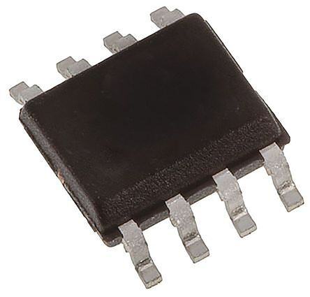
| 产品图片 |
|
| rohs | 符合RoHS无铅 / 符合限制有害物质指令(RoHS)规范要求 |
| 产品系列 | 放大器 IC,运算放大器 - 运放,STMicroelectronics TSV632IDT- |
| 数据手册 | |
| 产品型号 | TSV632IDT |
| 产品培训模块 | http://www.digikey.cn/PTM/IndividualPTM.page?site=cn&lang=zhs&ptm=23430 |
| 产品目录页面 | |
| 产品种类 | 运算放大器 - 运放 |
| 供应商器件封装 | 8-SO |
| 共模抑制比—最小值 | 60 dB |
| 关闭 | No Shutdown |
| 其它名称 | 497-8996-1 |
| 其它有关文件 | http://www.st.com/web/catalog/sense_power/FM123/SC61/SS1613/LN1588/PF187580?referrer=70071840http://www.st.com/web/catalog/sense_power/FM123/SC61/SS1613/LN1591/PF187580?referrer=70071840 |
| 包装 | 剪切带 (CT) |
| 压摆率 | 0.34 V/µs |
| 商标 | STMicroelectronics |
| 增益带宽生成 | 0.88 MHz |
| 增益带宽积 | 880kHz |
| 安装类型 | 表面贴装 |
| 安装风格 | SMD/SMT |
| 封装 | Reel |
| 封装/外壳 | 8-SOIC(0.154",3.90mm 宽) |
| 封装/箱体 | SO |
| 工作温度 | -40°C ~ 125°C |
| 工作电源电压 | 1.5 V to 5.5 V |
| 工厂包装数量 | 2500 |
| 技术 | CMOS |
| 放大器类型 | Low Voltage Amplifier |
| 最大工作温度 | + 125 C |
| 最小工作温度 | - 40 C |
| 标准包装 | 1 |
| 特色产品 | http://www.digikey.com/cn/zh/ph/st/tsv630.html |
| 电压-电源,单/双 (±) | 1.5 V ~ 5.5 V |
| 电压-输入失调 | 3mV |
| 电流-电源 | 60µA |
| 电流-输入偏置 | 1pA |
| 电流-输出/通道 | 74mA |
| 电源电流 | 60 uA |
| 电路数 | 2 |
| 系列 | TSV632 |
| 转换速度 | 0.34 V/us |
| 输入偏压电流—最大 | 10 pA |
| 输入参考电压噪声 | 60 nV |
| 输入补偿电压 | 3 mV |
| 输出电流 | 74 mA |
| 输出类型 | 满摆幅 |
| 通道数量 | 2 Channel |


- 商务部:美国ITC正式对集成电路等产品启动337调查
- 曝三星4nm工艺存在良率问题 高通将骁龙8 Gen1或转产台积电
- 太阳诱电将投资9.5亿元在常州建新厂生产MLCC 预计2023年完工
- 英特尔发布欧洲新工厂建设计划 深化IDM 2.0 战略
- 台积电先进制程称霸业界 有大客户加持明年业绩稳了
- 达到5530亿美元!SIA预计今年全球半导体销售额将创下新高
- 英特尔拟将自动驾驶子公司Mobileye上市 估值或超500亿美元
- 三星加码芯片和SET,合并消费电子和移动部门,撤换高东真等 CEO
- 三星电子宣布重大人事变动 还合并消费电子和移动部门
- 海关总署:前11个月进口集成电路产品价值2.52万亿元 增长14.8%


PDF Datasheet 数据手册内容提取
TSV63x, TSV63xA Dual and quad, rail-to-rail input/output, 60 µA, 880 kHz operational amplifiers Datasheet - production data Related products See the TSV52x series for higher merit factor (1.15 MHz for 45 µA) See the TSV61x (120 kHz for 9 µA) or TSV62x (420 kHz for 29 µA) for more power savings Applications Battery-powered applications Portable devices Signal conditioning Active filtering Medical instrumentation Description The TSV63x and TSV63xA series of dual and quad operational amplifiers offers low voltage operation and rail-to-rail input and output. This family features an excellent speed/power consumption ratio, offering an 880 kHz gain- bandwidth product while consuming only 60 µA at 5 V supply voltage. The devices also feature an ultralow input bias current and TSV633 and TSV635 have a shutdown mode. These features make the TSV63x and TSV63xA Features family ideal for sensor interfaces, battery- supplied and portable applications, and active Rail-to-rail input and output filtering. Low power consumption: 60 µA typ at 5 V Low supply voltage: 1.5 V - 5.5 V Table 1: Device summary Gain bandwidth product: 880 kHz typ Dual version Quad version Unity gain stable on 100 pF capacitor Reference Low power shutdown mode: 5 nA typ Without With Without With standby standby standby standby Low offset voltage: 800 µV max (A version) Low input bias current: 1 pA typ TSV63x TSV632 TSV633 TSV634 TSV635 EMI hardened op amps Automotive qualification TSV63xA TSV632A TSV633A TSV634A TSV635A May 2015 DocID15688 Rev 6 1/31 This is information on a product in full production. www.st.com
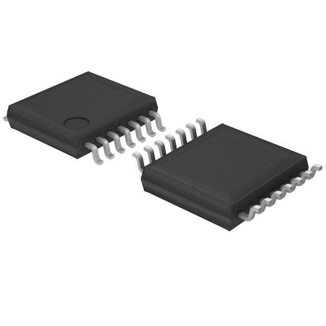
Contents TSV632, TSV632A, TSV633, TSV633A, TSV634, TSV634A, TSV635, TSV635A Contents 1 Package pin connections ................................................................ 3 2 Absolute maximum ratings and operating conditions ................. 4 3 Electrical characteristics ................................................................ 6 4 Application information ................................................................ 14 4.1 Operating voltages .......................................................................... 14 4.2 Rail-to-rail input ............................................................................... 14 4.3 Rail-to-rail output ............................................................................. 14 4.4 Shutdown function (TSV633, TSV635) ........................................... 15 4.5 Optimization of DC and AC parameters .......................................... 16 4.6 Driving resistive and capacitive loads ............................................. 16 4.7 PCB layouts .................................................................................... 16 4.8 Macromodel .................................................................................... 17 5 Package information ..................................................................... 18 5.1 DFN8 2 x 2 (NB) package information ............................................ 19 5.2 SOT23-8 package information ........................................................ 21 5.3 MiniSO8 package information ......................................................... 22 5.4 MiniSO10 package information ....................................................... 23 5.5 SO8 package information ................................................................ 24 5.6 QFN16 3x3 package information ..................................................... 25 5.7 TSSOP14 package information ....................................................... 27 5.8 TSSOP16 package information ....................................................... 28 6 Ordering information ..................................................................... 29 7 Revision history ............................................................................ 30 2/31 DocID15688 Rev 6
TSV632, TSV632A, TSV633, TSV633A, TSV634, Package pin connections TSV634A, TSV635, TSV635A 1 Package pin connections Figure 1: Pin connections for each package (top view) 1. The exposed pads of the DFN8 2x2 and the QFN16 3x3 can be connected to V or left floating. CC- DocID15688 Rev 6 3/31
Absolute maximum ratings and operating TSV632, TSV632A, TSV633, TSV633A, TSV634, conditions TSV634A, TSV635, TSV635A 2 Absolute maximum ratings and operating conditions Table 2: Absolute maximum ratings (AMR) Symbol Parameter Value Unit V Supply voltage (1) 6 CC V Differential input voltage (2) ±V V id CC V Input voltage (3) (V ) - 0.2 to (V ) + 0.2 in CC- CC+ I Input current (4) 10 mA in SHDN Shutdown voltage (3) (V ) - 0.2 to (V ) + 0.2 V CC- CC+ SHDN T Storage temperature -65 to 150 °C stg DFN8 2x2 57 SOT23-8 105 MiniSO8 190 MiniSO10 113 Thermal resistance junction to Rthja ambient (5)(6) °C/W SO8 125 QFN16 3x3 39 TSSOP14 100 TSSOP16 95 T Maximum junction temperature 150 °C j HBM: human body model (7) 4000 ESD MM: machine model (8) 300 V CDM: charged device model (9) 1500 Latch-up immunity 200 mA Notes: (1)All voltage values, except the differential voltage are with respect to the network ground terminal. (2)Differential voltages are the non-inverting input terminal with respect to the inverting input terminal. (3)VCC - VIN must not exceed 6 V, VIN must not exceed 6 V. (4)Input current must be limited by a resistor in series with the inputs (5)Rth are typical values (6)Short-circuits can cause excessive heating and destructive dissipation (7)Human body model: 100 pF discharged through a 1.5 kΩ resistor between two pins of the device, done for all couples of pin combinations with other pins floating. (8)Machine model: a 200 pF cap is charged to the specified voltage, then discharged directly between two pins of the device with no external series resistor (internal resistor < 5 Ω), done for all couples of pin combinations with other pins floating (9)Charged device model: all pins plus package are charged together to the specified voltage and then discharged directly to the ground. 4/31 DocID15688 Rev 6
TSV632, TSV632A, TSV633, TSV633A, TSV634, Absolute maximum ratings and operating TSV634A, TSV635, TSV635A conditions Table 3: Operating conditions Symbol Parameter Value Unit V Supply voltage 1.5 to 5.5 CC V V Common-mode input voltage range (V ) - 0.1 to (V ) + 0.1 ICM CC- CC+ T Operating free-air temperature range -40 to 125 °C oper DocID15688 Rev 6 5/31
Electrical characteristics TSV632, TSV632A, TSV633, TSV633A, TSV634, TSV634A, TSV635, TSV635A 3 Electrical characteristics Table 4: Electrical characteristics at VCC+ = 1.8 V with VCC- = 0 V, Vicm = VCC/2, Tamb = 25° C, and RL connected to VCC/2 (unless otherwise specified) Symbol Parameter Conditions Min. Typ. Max. Unit DC performance TSV63x 3 TSV63xA 0.8 TSV633AIST (MiniSO10) 1 V Offset voltage mV io T < T < T - TSV63x 4.5 min op max T < T < T - TSV63xA 2 min op max T < T < T - TSV633AIST 2.2 min op max ∆V /∆T Input offset voltage drift 2 μV/°C io (V = V /2) 1 10 (1) out CC I Input offset current io T < T < T 1 100 min op max pA (V = V /2) 1 10 (1) out CC I Input bias current ib T < T < T 1 100 min op max Common mode rejection 0 V to 1.8 V, Vout = 0.9 V 53 74 CMR ratio 20 log (ΔVic/ΔVio) Tmin < Top < Tmax 51 dB R = 10 kΩ, V = 0.5 V to 1.3 V 85 95 L out A Large signal voltage gain vd T < T < T 80 min op max V High level output voltage, RL = 10 kΩ 5 35 OH (VOH = VCC - Vout) Tmin < Top < Tmax 50 mV R = 10 kΩ 4 35 L V Low level output voltage OL T < T < T 50 min op max V = 1.8 V 6 12 o I sink T < T < T 4 min op max I mA out V = 0 V 6 10 o I source T < T < T 4 min op max Supply current No load, Vout = VCC/2 40 50 60 I µA CC (per channel) T < T < T 62 min op max AC performance GBP Gain bandwidth product R = 2 kΩ, C = 100 pF, f = 100 kHz 700 790 kHz L L ɸm Phase margin R = 2 kΩ, C = 100 pF 45 Degrees L L G Gain margin R = 2 kΩ, C = 100 pF 13 dB m L L SR Slew rate R = 2 kΩ, C = 100 pF, A = 1 0.2 0.27 V/μs L L v Equivalent input noise f = 1 kHz 60 e nV/√Hz n voltage f = 10 kHz 33 Notes: (1)Guaranteed by design 6/31 DocID15688 Rev 6
TSV632, TSV632A, TSV633, TSV633A, TSV634, Electrical characteristics TSV634A, TSV635, TSV635A Table 5: Shutdown characteristics VCC = 1.8 V Symbol Parameter Conditions Min. Typ. Max. Unit DC performance SHDN = V 2.5 50 CC- Supply current in shutdown nA I CC mode (all channels) Tmin < Top < 85° C 200 T < T < 125° C 1.5 µA min op R = 2 kΩ, V = (V ) to t Amplifier turn-on time L out CC- 200 on (VCC-) + 0.2 V ns R = 2 kΩ, V = (V ) - 0.5 V to t Amplifier turn-off time L out CC+ 20 off (VCC+) - 0.7 V V SHDN logic high 1.35 IH V V SHDN logic low 0.6 IL IIH SHDN current high SHDN = VCC+ 10 IIL SHDN current low SHDN = VCC- 10 pA Output leakage in shutdown SHDN = VCC- 50 I OLeak mode T < T < 125° C 1 nA min op DocID15688 Rev 6 7/31
Electrical characteristics TSV632, TSV632A, TSV633, TSV633A, TSV634, TSV634A, TSV635, TSV635A Table 6: VCC+ = 3.3 V, VCC- = 0 V, Vicm = VCC/2, Tamb = 25° C, RL connected to VCC/2 (unless otherwise specified) Symbol Parameter Conditions Min. Typ. Max. Unit DC performance TSV63x 3 TSV63xA 0.8 TSV633AIST (MiniSO10) 1 V Offset voltage mV io T < T < T - TSV63x 4.5 min op max T < T < T - TSV63xA 2 min op max T < T < T - TSV633AIST 2.2 min op max ∆V /∆T Input offset voltage drift 2 μV/°C io V = V /2 1 10 (1) out CC I Input offset current io T < T < T 1 100 min op max pA V = V /2 1 10 (1) out CC I Input bias current ib T < T < T 1 100 min op max Common mode rejection 0 V to 3.3 V, Vout = 1.65 V 57 79 CMR ratio 20 log (ΔVic/ΔVio) Tmin < Top < Tmax 53 dB R = 10 kΩ, V = 0.5 V to 2.8 V 88 98 L out A Large signal voltage gain vd T < T < T 83 min op max V High level output voltage, RL = 10 kΩ 5 35 OH (VOH = VCC - Vout) Tmin < Top < Tmax 50 mV R = 10 kΩ 4 35 L V Low level output voltage OL T < T < T 50 min op max V = 3.3 V 23 45 o I sink T < T < T 20 min op max I mA out V = 0 V 23 38 o I source T < T < T 20 min op max Supply current, No load, Vout = 1.75 V 43 55 64 I µA CC (per channel) T < T < T 66 min op max AC performance R = 2 kΩ, C = 100 pF, GBP Gain bandwidth product L L 710 860 kHz f = 100 kHz ɸm Phase margin R = 2 kΩ, C = 100 pF 46 Degrees L L G Gain margin R = 2 kΩ, C = 100 pF 13 dB m L L SR Slew rate R = 2 kΩ, C = 100 pF, A = 1 0.22 0.29 V/μs L L V Notes: (1)Guaranteed by design 8/31 DocID15688 Rev 6
TSV632, TSV632A, TSV633, TSV633A, TSV634, Electrical characteristics TSV634A, TSV635, TSV635A Table 7: Electrical characteristics at VCC+ = 5 V with VCC- = 0 V, Vicm = VCC/2, Tamb = 25° C, and RL connected to VCC/2 (unless otherwise specified) Symbol Parameter Conditions Min. Typ. Max. Unit DC performance TSV63x 3 TSV63xA 0.8 TSV633AIST ( MiniSO10) 1 V Offset voltages mV io T < T < T - TSV63x 4.5 min op max T < T < T - TSV63xA 2 min op max T < T < T - TSV633AIST 2.2 min op max ∆V /∆T Input offset voltage drift 2 μV/°C io (V = V /2) 1 10 (1) out CC I Input offset current io T < T < T 1 100 min op max pA (V = V /2) 1 10 (1) out CC I Input bias current ib T < T < T 1 100 min op max Common mode rejection 0 V to 5 V, Vout = 2.5 V 60 80 CMR ratio 20 log (ΔVic/ΔVio) Tmin < Top < Tmax 55 Supply voltage rejection VCC = 1.8 to 5 V 75 102 SVR ratio 20 log (ΔVCC/ΔVio) Tmin < Top < Tmax 73 R = 10 kΩ, V = 0.5 V to 4.5 V 89 98 L out A Large signal voltage gain dB vd T < T < T 84 min op max V = 100 mV , f = 400 MHz 61 RF rms EMI rejection ratio, EMIRR VRF = 100 mVrms, f = 900 MHz 85 EMIRR = -20 log (VRFpeak/ΔVio) VRF = 100 mVrms, f = 1800 MHz 92 V = 100 mV , f = 2400 MHz 83 RF rms V High level output voltage, RL = 10 kΩ 7 35 OH (VOH = VCC - Vout) Tmin < Top < Tmax 50 mV R = 10 kΩ 6 35 L V Low level output voltage OL T < T < T 50 min op max V = 5 V 40 69 o I sink T < T < T 35 min op max I mA out V = 0 V 40 74 o I source T < T < T 35 min op max Supply current, No load, Vout = VCC/2 50 60 69 I µA CC (per channel) T < T < T 72 min op max AC performance R = 2 kΩ, C = 100 pF, GBP Gain bandwidth product L L 730 880 f = 100 kHz kHz F Unity gain frequency R = 2 kΩ, C = 100 pF 830 u L L ɸm Phase margin R = 2 kΩ, C = 100 pF 48 Degrees L L DocID15688 Rev 6 9/31
Electrical characteristics TSV632, TSV632A, TSV633, TSV633A, TSV634, TSV634A, TSV635, TSV635A Symbol Parameter Conditions Min. Typ. Max. Unit G Gain margin R = 2 kΩ, C = 100 pF 13 dB m L L SR Slew rate R = 2 kΩ, C = 100 pF, A =1 0.25 0.34 V/μs L L v Equivalent input noise f = 1 kHz 60 e nV/√Hz n voltage f = 10 kHz 33 Total harmonic distortion + V = 5V, f = 1 kHz, A = 1, R = THD+e CC v L 0.002 % n noise 100 kΩ, Vicm = VCC/2, Vout = 2Vpp Notes: (1)Guaranteed by design Table 8: Shutdown characteristics at VCC = 5 V Symbol Parameter Conditions Min. Typ. Max. Unit DC performance SHDN = VCC- 5 50 Supply current in shutdown nA I CC mode (all channels) Tmin < Top < 85° C 200 T < T < 125° C 1.5 µA min op R = 2 kΩ, V = (V ) to t Amplifier turn-on time L out CC- 200 on (VCC-) + 0.2 V ns R = 2 kΩ, V = (V ) - 0.5 V to t Amplifier turn-off time L out CC+ 20 off (VCC+) - 0.7 V V SHDN logic high 2 IH V V SHDN logic low 0.8 IL I SHDN current high SHDN = V 10 IH CC+ IIL SHDN current low SHDN = VCC- 10 pA Output leakage in shutdown SHDN = VCC- 50 I OLeak mode T < T < 125 °C 1 nA min op 10/31 DocID15688 Rev 6
TSV632, TSV632A, TSV633, TSV633A, TSV634, Electrical characteristics TSV634A, TSV635, TSV635A Figure 2: Supply current vs. supply voltage Figure 3: Output current vs. output voltage at Vicm = VCC/2 at VCC = 1.5 V Figure 4: Output current vs. output voltage Figure 5: Voltage gain and phase vs. frequency at VCC = 5 V at VCC = 1.5 V Ω Figure 6: Voltage gain and phase vs. frequency Figure 7: Phase margin vs. output current at VCC = 5 V at VCC = 5 V DocID15688 Rev 6 11/31
Electrical characteristics TSV632, TSV632A, TSV633, TSV633A, TSV634, TSV634A, TSV635, TSV635A Figure 8: Positive slew rate vs. time Figure 9: Negative slew rate vs. time Figure 10: Positive slew rate vs. supply voltage Figure 11: Negative slew rate vs. supply voltage Figure 12: Distortion + noise vs. output voltage Figure 13: Distortion + noise vs. frequency 1 Vcc = 1.5 V Vcc = 1.5 V Vcc = 1.5 V Av = 1 Rl = 2 kΩ Rl = 2 kΩ Rl = 100 kΩ Vin = 1 Vpp BW = 80 kHz 0.1 Vicm = Vcc/2 (%) %) Vcc = 1.5 V N N ( Rl = 100 kΩ + + D D H H T T 0.01 Vcc = 5.5 V f = 1 kHz Vcc = 5.5 V Rl = 2 kΩ Gain = 1 Rl = 2 kΩ BW = 22 kHz Vicm = Vcc/2 Vcc = 5.5 V Vcc = 5.5 V Rl = 100 kΩ Rl = 100 kΩ 1E-3 10 100 1000 10000 100000 OutputVoltage(Vpp) 12/31 DocID15688 Rev 6
TSV632, TSV632A, TSV633, TSV633A, TSV634, Electrical characteristics TSV634A, TSV635, TSV635A Figure 14: Noise vs. frequency Figure 15: EMIRR vs. frequency at VCC = 5 V, T = 25 °C z) 300 112200 H V/V Vcc=5V (n 250 Tamb=25°C 110000 e s Noi 200 B) 8800 e Vicm=2.5V d g ( Volta 150 RVpeak 6600 ut R p IM In 100 E 4400 nt e al Vicm=4.5V quiv 50 2200 E 0 00 100 1000 10000 101 102 103 DocID15688 Rev 6 13/31
Application information TSV632, TSV632A, TSV633, TSV633A, TSV634, TSV634A, TSV635, TSV635A 4 Application information 4.1 Operating voltages The TSV63x and TSV63xA can operate from 1.5 to 5.5 V. Their parameters are fully specified for 1.8 V, 3.3 V, and 5 V power supplies. However, the parameters are very stable in the full V range and several characterization curves show the TSV63x and CC TSV63xA characteristics at 1.5 V. Additionally, the main specifications are guaranteed in extended temperature ranges from -40 °C to 125 °C. 4.2 Rail-to-rail input The TSV63x and TSV63xA are built with two complementary PMOS and NMOS input differential pairs. The devices have a rail-to-rail input and the input common mode range is extended from (V ) - 0.1 V to (V ) + 0.1 V. The transition between the two pairs appears CC- CC+ at (VCC+) - 0.7 V. In the transition region, the performance of CMRR, PSRR, Vio (Figure 16 and Figure 17), and THD is slightly degraded. Figure 16: Input offset voltage vs input common mode Figure 17: Input offset voltage vs input common mode voltage at VCC = 1.5 V voltage at VCC = 5 V The devices are guaranteed without phase reversal. 4.3 Rail-to-rail output The operational amplifiers’ output levels can go close to the rails: 35 mV maximum above and below the rail when connected to a 10 kΩ resistive load to V /2. CC 14/31 DocID15688 Rev 6
TSV632, TSV632A, TSV633, TSV633A, TSV634, Application information TSV634A, TSV635, TSV635A 4.4 Shutdown function (TSV633, TSV635) The operational amplifiers are enabled when the SHDN pin is pulled high. To disable the amplifiers, the SHDN must be pulled down to V . When in shutdown mode, the CC- amplifiers’ output is in a high impedance state. The SHDN pin must never be left floating, but tied to V or V . CC+ CC- The turn-on and turn-off times are calculated for an output variation of ±200 mV. Figure 18 and Figure 19 show the test configurations. Figure 20 shows the time it takes the product to come out of shutdown mode and Figure 21 shows the time it takes the product to enter shutdown mode. Figure 19: Test configuration for turn-off time (Vout Figure 18: Test configuration for turn-on time (Vout pulled down) pulled down) +Vcc +Vcc GND GND Ω Ω k k 2 2 Vcc-0.5V + Vcc-0.5V + DUT DUT - - GND GND Figure 20: Turn-on time, VCC = 5 V, Vout pulled down, Figure 21: Turn-off time, VCC = 5 V, Vout pulled down, T = 25° C T = 25° C 25° °C µ µ DocID15688 Rev 6 15/31
Application information TSV632, TSV632A, TSV633, TSV633A, TSV634, TSV634A, TSV635, TSV635A 4.5 Optimization of DC and AC parameters These devices use an innovative approach to reduce the spread of the main DC and AC parameters. An internal adjustment achieves a very narrow spread of the current consumption (60 µA typical, min/max at ±17 %). Parameters linked to the current consumption value, such as GBP, SR, and A , benefit from this narrow dispersion. All vd parts present a similar speed and the same behavior in terms of stability. In addition, the minimum values of GBP and SR are guaranteed (GBP = 730 kHz minimum and SR = 0.25 V/µs minimum). 4.6 Driving resistive and capacitive loads These products are micropower, low-voltage, operational amplifiers optimized to drive rather large resistive loads, above 2 kΩ. For lower resistive loads, the THD level may significantly increase. In a follower configuration, these operational amplifiers can drive capacitive loads up to 100 pF with no oscillations. When driving larger capacitive loads, adding an in-series resistor at the output can improve the stability of the devices (see Figure 22 for recommended in-series resistor values). Once the in-series resistor value has been selected, the stability of the circuit should be tested on the bench and simulated with the simulation model. Figure 22: In-series resistor vs. capacitive load 4.7 PCB layouts For correct operation, it is advised to add 10 nF decoupling capacitors as close as possible to the power supply pins. 16/31 DocID15688 Rev 6
TSV632, TSV632A, TSV633, TSV633A, TSV634, Application information TSV634A, TSV635, TSV635A 4.8 Macromodel Two accurate macromodels (with or without the shutdown feature) of the TSV63x and TSV63xA are available on STMicroelectronics’ web site at www.st.com. These models are a trade-off between accuracy and complexity (that is, time simulation) of the TSV63x and TSV63xA operational amplifiers. They emulate the nominal performances of a typical device within the specified operating conditions mentioned in the datasheet. They also help to validate a design approach and to select the right operational amplifier, but they do not replace on-board measurements. DocID15688 Rev 6 17/31
Package information TSV632, TSV632A, TSV633, TSV633A, TSV634, TSV634A, TSV635, TSV635A 5 Package information In order to meet environmental requirements, ST offers these devices in different grades of ECOPACK® packages, depending on their level of environmental compliance. ECOPACK® specifications, grade definitions and product status are available at: www.st.com. ECOPACK® is an ST trademark. 18/31 DocID15688 Rev 6
TSV632, TSV632A, TSV633, TSV633A, TSV634, Package information TSV634A, TSV635, TSV635A 5.1 DFN8 2 x 2 (NB) package information Figure 23: DFN8 2 x 2 mm (NB) package outline Table 9: DFN8 2 x 2 x 0.6 mm (NB) package mechanical data (pitch 0.5 mm) Dimensions Ref. Millimeters Inches Min. Typ. Max. Min. Typ. Max. A 0.51 0.55 0.60 0.020 0.022 0.024 A1 0.05 0.002 A3 0.15 0.006 b 0.18 0.25 0.30 0.007 0.010 0.012 D 1.85 2.00 2.15 0.073 0.079 0.085 D2 1.45 1.60 1.70 0.057 0.063 0.067 E 1.85 2.00 2.15 0.073 0.079 0.085 E2 0.75 0.90 1.00 0.030 0.035 0.039 e 0.50 0.020 L 0.425 0.017 ddd 0.08 0.003 DocID15688 Rev 6 19/31
Package information TSV632, TSV632A, TSV633, TSV633A, TSV634, TSV634A, TSV635, TSV635A Figure 24: DFN8 2 x 2 mm (NB) recommended footprint 20/31 DocID15688 Rev 6
TSV632, TSV632A, TSV633, TSV633A, TSV634, Package information TSV634A, TSV635, TSV635A 5.2 SOT23-8 package information Figure 25: SOT23-8 package outline SIDE VIEW Dimensions in mm A A2 Gauge plane A1 L 0.1 C coplanar leads D C e1 e 0.25 Seating plane e/2 E/2 E1/2 E E1 c b (8x leads) TOP VIEW projection Table 10: SOT23-8 package mechanical data Dimensions Ref. Millimeters Inches Min. Typ. Max. Min. Typ. Max. A 1.45 0.057 A1 0.15 0.006 A2 0.90 1.30 0.035 0.051 b 0.22 0.38 0.009 0.015 c 0.08 0.22 0.003 0.009 D 2.80 3.00 0.110 0.118 E 2.60 3.00 0.102 0.118 E1 1.50 1.75 0.059 0.069 e 0.65 0.026 e1 1.95 0.077 L 0.30 0.60 0.012 0.024 < 0° 8° 0° 8° DocID15688 Rev 6 21/31
Package information TSV632, TSV632A, TSV633, TSV633A, TSV634, TSV634A, TSV635, TSV635A 5.3 MiniSO8 package information Figure 26: MiniSO8 package outline Table 11: MiniSO8 package mechanical data Dimensions Ref. Millimeters Inches Min. Typ. Max. Min. Typ. Max. A 1.1 0.043 A1 0 0.15 0 0.006 A2 0.75 0.85 0.95 0.030 0.033 0.037 b 0.22 0.40 0.009 0.016 c 0.08 0.23 0.003 0.009 D 2.80 3.00 3.20 0.11 0.118 0.126 E 4.65 4.90 5.15 0.183 0.193 0.203 E1 2.80 3.00 3.10 0.11 0.118 0.122 e 0.65 0.026 L 0.40 0.60 0.80 0.016 0.024 0.031 L1 0.95 0.037 L2 0.25 0.010 k 0° 8° 0° 8° ccc 0.10 0.004 22/31 DocID15688 Rev 6
TSV632, TSV632A, TSV633, TSV633A, TSV634, Package information TSV634A, TSV635, TSV635A 5.4 MiniSO10 package information Figure 27: MiniSO10 package outline Table 12: MiniSO-10 package mechanical data Dimensions Ref. Millimeters Inches Min. Typ. Max. Min. Typ. Max. A 1.10 0.043 A1 0.05 0.10 0.15 0.002 0.004 0.006 A2 0.78 0.86 0.94 0.031 0.034 0.037 b 0.25 0.33 0.40 0.010 0.013 0.016 c 0.15 0.23 0.30 0.006 0.009 0.012 D 2.90 3.00 3.10 0.114 0.118 0.122 E 4.75 4.90 5.05 0.187 0.193 0.199 E1 2.90 3.00 3.10 0.114 0.118 0.122 e 0.50 0.020 L 0.40 0.55 0.70 0.016 0.022 0.028 L1 0.95 0.037 k 0° 3° 6° 0° 3° 6° aaa 0.10 0.004 DocID15688 Rev 6 23/31
Package information TSV632, TSV632A, TSV633, TSV633A, TSV634, TSV634A, TSV635, TSV635A 5.5 SO8 package information Figure 28: SO8 package outline Table 13: SO8 package mechanical data Dimensions Ref. Millimeters Inches Min. Typ. Max. Min. Typ. Max. A 1.75 0.069 A1 0.10 0.25 0.004 0.010 A2 1.25 0.049 b 0.28 0.48 0.011 0.019 c 0.17 0.23 0.007 0.010 D 4.80 4.90 5.00 0.189 0.193 0.197 E 5.80 6.00 6.20 0.228 0.236 0.244 E1 3.80 3.90 4.00 0.150 0.154 0.157 e 1.27 0.050 h 0.25 0.50 0.010 0.020 L 0.40 1.27 0.016 0.050 L1 1.04 0.040 k 1° 8° 1° 8° ccc 0.10 0.004 24/31 DocID15688 Rev 6
TSV632, TSV632A, TSV633, TSV633A, TSV634, Package information TSV634A, TSV635, TSV635A 5.6 QFN16 3x3 package information Figure 29: QFN16 3x3 mm package outline DocID15688 Rev 6 25/31
Package information TSV632, TSV632A, TSV633, TSV633A, TSV634, TSV634A, TSV635, TSV635A Table 14: QFN16 3x3 mm package mechanical data Dimensions Ref. Millimeters Inches Min. Typ. Max. Min. Typ. Max. A 0.80 0.90 1.00 0.031 0.035 0.039 A1 0 0.05 0 0.002 A3 0.20 0.008 b 0.18 0.30 0.007 0.012 D 2.90 3.00 3.10 0.114 0.118 0.122 D2 1.50 1.80 0.059 0.071 E 2.90 3.00 3.10 0.114 0.118 0.122 E2 1.50 1.80 0.059 0.071 e 0.50 0.020 L 0.30 0.50 0.012 0.020 Figure 30: QFN16 3x3 mm recommended footprint 26/31 DocID15688 Rev 6
TSV632, TSV632A, TSV633, TSV633A, TSV634, Package information TSV634A, TSV635, TSV635A 5.7 TSSOP14 package information Figure 31: TSSOP14 package outline Table 15: TSSOP14 package mechanical data Dimensions Ref. Millimeters Inches Min. Typ. Max. Min. Typ. Max. A 1.20 0.047 A1 0.05 0.15 0.002 0.004 0.006 A2 0.80 1.00 1.05 0.031 0.039 0.041 b 0.19 0.30 0.007 0.012 c 0.09 0.20 0.004 0.0089 D 4.90 5.00 5.10 0.193 0.197 0.201 E 6.20 6.40 6.60 0.244 0.252 0.260 E1 4.30 4.40 4.50 0.169 0.173 0.176 e 0.65 0.0256 L 0.45 0.60 0.75 0.018 0.024 0.030 L1 1.00 0.039 k 0° 8° 0° 8° aaa 0.10 0.004 DocID15688 Rev 6 27/31
Package information TSV632, TSV632A, TSV633, TSV633A, TSV634, TSV634A, TSV635, TSV635A 5.8 TSSOP16 package information Figure 32: TSSOP16 package outline Table 16: TSSOP16 package mechanical data Dimensions Ref. Millimeters Inches Min. Typ. Max. Min. Typ. Max. A 1.20 0.047 A1 0.05 0.15 0.002 0.006 A2 0.80 1.00 1.05 0.031 0.039 0.041 b 0.19 0.30 0.007 0.012 c 0.09 0.20 0.004 0.008 D 4.90 5.00 5.10 0.193 0.197 0.201 E 6.20 6.40 6.60 0.244 0.252 0.260 E1 4.30 4.40 4.50 0.169 0.173 0.177 e 0.65 0.026 k 0° 8° 0° 8° L 0.45 0.60 0.75 0.018 0.024 0.030 L1 1.00 0.039 aaa 0.10 0.004 28/31 DocID15688 Rev 6
TSV632, TSV632A, TSV633, TSV633A, TSV634, Ordering information TSV634A, TSV635, TSV635A 6 Ordering information Table 17: Order codes Order code Temperature range Package (1) Marking TSV632AIDT SO8 TV632A TSV632AILT SOT23-8 K145 TSV632AIQ2T DFN8 2x2 K1P TSV632AIST MiniSO8 K145 -40 °C to 125 °C TSV632IDT SΟ8 TSV632 TSV632ILT SOT23-8 K110 TSV632IQ2T DFN8 2x2 K1N TSV632IST MiniSO8 K110 -40 °C to 125 °C, TSV632IYDT SΟ8 V632IY automotive grade (2) TSV633AIST K146 MiniSO10 TSV633IST K111 TSV634AIPT -40 °C to 125 °C TSSOP14 TSV634A TSV634IQ4T QFN16 3x3 K112 TSV634IPT TSV634 -40 °C to 125 °C, TSSOP14 TSV634IYPT V634IY automotive grade (2) TSV635AIPT TSV635A -40 °C to 125 °C TSSOP16 TSV635IPT TSV635 Notes: (1)All devices are in tape and reel packing (2)Qualified and characterized according to AEC Q100 and Q003 or equivalent, advanced screening according to AEC Q001 and Q002. DocID15688 Rev 6 29/31
Revision history TSV632, TSV632A, TSV633, TSV633A, TSV634, TSV634A, TSV635, TSV635A 7 Revision history Table 18: Document revision history Date Revision Changes 25-May-2009 1 Initial release. 15-Jun-2009 2 Corrected pin connection diagram in Figure 1. Added root part numbers (TSV63xA) and Table 1: "Device 03-Sep-2009 3 summary" on cover page. Added order code TSV632AILT in Table 17: "Order codes". Added DFN8 2x2 package mechanical drawing. Added ordering information for DFN package to Table 17: "Order 07-Nov-2011 4 codes". Corrected unit on Y axis of Figure 16 and Figure 17. Updated Features Added QFN16 3x3 package Updated Figure 1: "Pin connections for each package (top view)". Table 4, Table 6, and Table 7: replaced DV symbol with ∆V /∆T io io Table 4, Table 5, Table 6, Table 7 and Table 8: for supply current 13-Dec-2012 5 parameter, replaced “operator” with “channel”. Table 17: "Order codes": added automotive order codes and updated footnote Deleted TSV632ID/AID from order codes in Table 17: "Order codes" Table 4, Table 6, and Table 7: V "min" values changed to "max" OH values. 29-May-2015 6 Table 17: "Order codes": added order code TSV632AIQ2T, updated footnote 1. 30/31 DocID15688 Rev 6
TSV632, TSV632A, TSV633, TSV633A, TSV634, TSV634A, TSV635, TSV635A IMPORTANT NOTICE – PLEASE READ CAREFULLY STMicroelectronics NV and its subsidiaries (“ST”) reserve the right to make changes, corrections, enhancements, modifications, and improvements to ST products and/or to this document at any time without notice. Purchasers should obtain the latest relevant information on ST products before placing orders. ST products are sold pursuant to ST’s terms and conditions of sale in place at the time of order acknowledgement. Purchasers are solely responsible for the choice, selection, and use of ST products and ST assumes no liability for application assistance or the design of Purchasers’ products. No license, express or implied, to any intellectual property right is granted by ST herein. Resale of ST products with provisions different from the information set forth herein shall void any warranty granted by ST for such product. ST and the ST logo are trademarks of ST. All other product or service names are the property of their respective owners. Information in this document supersedes and replaces information previously supplied in any prior versions of this document. © 2015 STMicroelectronics – All rights reserved DocID15688 Rev 6 31/31