ICGOO在线商城 > 集成电路(IC) > 线性 - 放大器 - 仪表,运算放大器,缓冲器放大器 > AD620BNZ
 Datasheet下载
- 型号: AD620BNZ
- 制造商: Analog
- 库位|库存: xxxx|xxxx
- 要求:
| 数量阶梯 | 香港交货 | 国内含税 |
| +xxxx | $xxxx | ¥xxxx |
查看当月历史价格
查看今年历史价格
AD620BNZ产品简介:
ICGOO电子元器件商城为您提供AD620BNZ由Analog设计生产,在icgoo商城现货销售,并且可以通过原厂、代理商等渠道进行代购。 AD620BNZ价格参考¥109.98-¥150.09。AnalogAD620BNZ封装/规格:线性 - 放大器 - 仪表,运算放大器,缓冲器放大器, Instrumentation Amplifier 1 Circuit 8-PDIP。您可以下载AD620BNZ参考资料、Datasheet数据手册功能说明书,资料中有AD620BNZ 详细功能的应用电路图电压和使用方法及教程。
AD620BNZ是Analog Devices Inc.生产的一款高精度、低功耗的仪表放大器,广泛应用于需要精确信号放大的场合。其典型应用场景包括工业测量、医疗设备、传感器信号调理和数据采集系统。

在医疗领域,AD620BNZ常用于心电图(ECG)、脑电图(EEG)等生物电信号采集系统中,因其具有高共模抑制比(CMRR)、低噪声和低输入偏置电流,能够有效放大微弱的生理信号并抑制环境干扰。在工业自动化中,该器件适用于压力、温度、应变片等传感器的信号调理,将微小的差分信号转换为标准输出信号,提高测量精度。此外,在精密测试仪器和便携式设备中,AD620BNZ凭借其低功耗(最大供电电流仅1.3mA)和宽电源电压范围(±2.3V至±18V),也表现出良好的适应性。

AD620BNZ采用8引脚DIP封装(BNZ后缀),便于手工焊接与原型开发,适合实验室和小批量应用。其增益通过单个外部电阻即可精确设置(增益范围1至1000),使用灵活,外围电路简洁。总体而言,AD620BNZ是一款性能稳定、可靠性高的仪表放大器,特别适用于对精度和稳定性要求较高的模拟信号放大场景。
| 参数 | 数值 |
| -3db带宽 | 1MHz |
| 产品目录 | 集成电路 (IC)半导体 |
| 描述 | IC OPAMP INSTR 1MHZ 8DIP仪表放大器 Low Drift Low Power |
| 产品分类 | Linear - Amplifiers - Instrumentation, OP Amps, Buffer Amps集成电路 - IC |
| 品牌 | Analog Devices Inc |
| 产品手册 | |
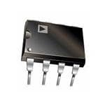
| 产品图片 |
|
| rohs | 符合RoHS无铅 / 符合限制有害物质指令(RoHS)规范要求 |
| 产品系列 | 放大器 IC,仪表放大器,Analog Devices AD620BNZ- |
| 数据手册 | |
| 产品型号 | AD620BNZ |
| 产品培训模块 | http://www.digikey.cn/PTM/IndividualPTM.page?site=cn&lang=zhs&ptm=25193http://www.digikey.cn/PTM/IndividualPTM.page?site=cn&lang=zhs&ptm=30008http://www.digikey.cn/PTM/IndividualPTM.page?site=cn&lang=zhs&ptm=26202 |
| 产品目录页面 | |
| 产品种类 | 仪表放大器 |
| 供应商器件封装 | 8-PDIP |
| 共模抑制比—最小值 | 120 dB |
| 包装 | 管件 |
| 压摆率 | 1.2 V/µs |
| 双重电源电压 | +/- 3 V, +/- 5 V, +/- 9 V, +/- 12 V, +/- 15 V |
| 可用增益调整 | 1 V/V to 10000 V/V |
| 商标 | Analog Devices |
| 增益带宽积 | - |
| 安装类型 | 通孔 |
| 安装风格 | Through Hole |
| 封装 | Tube |
| 封装/外壳 | 8-DIP(0.300",7.62mm) |
| 封装/箱体 | PDIP-8 |
| 工作温度 | -40°C ~ 85°C |
| 工作温度范围 | - 40 C to + 85 C |
| 工作电源电压 | 2.3 V to 18 V |
| 工厂包装数量 | 50 |
| 带宽 | 1000 kHz |
| 放大器类型 | 仪表 |
| 最大功率耗散 | 650 mW |
| 最大工作温度 | + 85 C |
| 最大输入电阻 | 10 GOhms at +/- 15 V |
| 最小工作温度 | - 40 C |
| 标准包装 | 50 |
| 电压-电源,单/双 (±) | 4.6 V ~ 36 V, ±2.3 V ~ 18 V |
| 电压-输入失调 | 15µV |
| 电流-电源 | 900µA |
| 电流-输入偏置 | 500pA |
| 电流-输出/通道 | 18mA |
| 电源电流 | 0.9 mA |
| 电路数 | 1 |
| 系列 | AD620 |
| 视频文件 | http://www.digikey.cn/classic/video.aspx?PlayerID=1364138032001&width=640&height=505&videoID=2245193153001http://www.digikey.cn/classic/video.aspx?PlayerID=1364138032001&width=640&height=505&videoID=2245193159001 |
| 设计资源 | |
| 转换速度 | 1.2 V/us |
| 输入偏压电流—最大 | 1 nA |
| 输入补偿电压 | 15 uV |
| 输出类型 | - |
| 通道数量 | 1 Channel |


- 商务部:美国ITC正式对集成电路等产品启动337调查
- 曝三星4nm工艺存在良率问题 高通将骁龙8 Gen1或转产台积电
- 太阳诱电将投资9.5亿元在常州建新厂生产MLCC 预计2023年完工
- 英特尔发布欧洲新工厂建设计划 深化IDM 2.0 战略
- 台积电先进制程称霸业界 有大客户加持明年业绩稳了
- 达到5530亿美元!SIA预计今年全球半导体销售额将创下新高
- 英特尔拟将自动驾驶子公司Mobileye上市 估值或超500亿美元
- 三星加码芯片和SET,合并消费电子和移动部门,撤换高东真等 CEO
- 三星电子宣布重大人事变动 还合并消费电子和移动部门
- 海关总署:前11个月进口集成电路产品价值2.52万亿元 增长14.8%


PDF Datasheet 数据手册内容提取
Low Cost Low Power Instrumentation Amplifier AD620 FEATURES CONNECTION DIAGRAM Easy to use Gain set with one external resistor (Gain range 1 to 10,000) RG 1 8 RG Wide power supply range (±2.3 V to ±18 V) –IN 2 7 +VS Higher performance than 3 op amp IA designs +IN 3 6 OUTPUT ExALceovlwalei lpnaotb wdlece irpn,e 18r.-f3loe mramdAa DmnIcPaex a ( snBud gp SrpaOldyIeC c) up rarceknatg ing –VS 4 TAODP 6V2IE0W 5 REF 00775-0-001 50 μV max, input offset voltage Figure 1. 8-Lead PDIP (N), CERDIP (Q), and SOIC (R) Packages 0.6 μV/°C max, input offset drift PRODUCT DESCRIPTION 1.0 nA max, input bias current The AD620 is a low cost, high accuracy instrumentation 100 dB min common-mode rejection ratio (G = 10) amplifier that requires only one external resistor to set gains of Low noise 1 to 10,000. Furthermore, the AD620 features 8-lead SOIC and 9 nV/√Hz @ 1 kHz, input voltage noise DIP packaging that is smaller than discrete designs and offers 0.28 μV p-p noise (0.1 Hz to 10 Hz) lower power (only 1.3 mA max supply current), making it a Excellent ac specifications good fit for battery-powered, portable (or remote) applications. 120 kHz bandwidth (G = 100) 15 μs settling time to 0.01% The AD620, with its high accuracy of 40 ppm maximum nonlinearity, low offset voltage of 50 μV max, and offset drift of APPLICATIONS 0.6 μV/°C max, is ideal for use in precision data acquisition Weigh scales systems, such as weigh scales and transducer interfaces. ECG and medical instrumentation Furthermore, the low noise, low input bias current, and low power Transducer interface of the AD620 make it well suited for medical applications, such as ECG and noninvasive blood pressure monitors. Data acquisition systems Industrial process controls The low input bias current of 1.0 nA max is made possible with Battery-powered and portable equipment the use of Superϐeta processing in the input stage. The AD620 works well as a preamplifier due to its low input voltage noise of 9 nV/√Hz at 1 kHz, 0.28 μV p-p in the 0.1 Hz to 10 Hz band, and 0.1 pA/√Hz input current noise. Also, the AD620 is well suited for multiplexed applications with its settling time of 15 μs to 0.01%, and its cost is low enough to enable designs with one in-amp per channel. Table 1. Next Generation Upgrades for AD620 30,000 Part Comment AD8221 Better specs at lower price CALE25,000 3 I NO-AP MAPMP AD8222 Dual channel or differential out ULL S20,000 (3 OP-07s) AD8226 Low power, wide input range OF F AD8220 JFET input PM 15,000 AD8228 Best gain accuracy OR, P AD620A AD8295 +2 precision op amps or differential out AL ERR10,000 RG AD8429 Ultra low noise OT 5,000 T 00 5 SUPPLY CU1R0RENT (mA) 15 2000775-0-002 Figure 2. Three Op Amp IA Designs vs. AD620 Rev. H Information furnished by Analog Devices is believed to be accurate and reliable. However, no responsibility is assumed by Analog Devices for its use, nor for any infringements of patents or other rights of third parties that may result from its use. One Technology Way, P.O. Box 9106, Norwood, MA 02062-9106, U.S.A. Specifications subject to change without notice. No license is granted by implication or otherwise under any patent or patent rights of Analog Devices. Trademarks and Tel: 781.329.4700 www.analog.com registered trademarks are the property of their respective owners. Fax: 781.326.8703© 2003–2011 Analog Devices, Inc. All rights reserved.
AD620 TABLE OF CONTENTS Specifications.....................................................................................3 RF Interference............................................................................15 Absolute Maximum Ratings............................................................5 Common-Mode Rejection.........................................................16 ESD Caution..................................................................................5 Grounding....................................................................................16 Typical Performance Characteristics..............................................6 Ground Returns for Input Bias Currents.................................17 Theory of Operation.......................................................................12 AD620ACHIPS Information.........................................................18 Gain Selection..............................................................................15 Outline Dimensions........................................................................19 Input and Output Offset Voltage..............................................15 Ordering Guide...........................................................................20 Reference Terminal.....................................................................15 Input Protection..........................................................................15 REVISION HISTORY 7/11—Rev. G to Rev. H Changes to Input Protection section............................................15 Deleted Figure 9..............................................................................15 Deleted Figure 3.................................................................................1 Changes to RF Interference section..............................................15 Added Table 1....................................................................................1 Edit to Ground Returns for Input Bias Currents section...........17 Moved Figure 2..................................................................................1 Added AD620CHIPS to Ordering Guide....................................19 Added ESD Input Diodes to Simplified Schematic....................12 Changes to Input Protection Section............................................15 Added Figure 41; Renumbered Sequentially...............................15 7/03—Data Sheet Changed from Rev. E to Rev. F Changes to AD620ACHIPS Information Section......................18 Edit to FEATURES............................................................................1 Updated Ordering Guide...............................................................20 Changes to SPECIFICATIONS.......................................................2 Removed AD620CHIPS from ORDERING GUIDE...................4 Removed METALLIZATION PHOTOGRAPH...........................4 12/04—Rev. F to Rev. G Replaced TPCs 1–3...........................................................................5 Updated Format..................................................................Universal Replaced TPC 12...............................................................................6 Change to Features............................................................................1 Replaced TPC 30...............................................................................9 Change to Product Description.......................................................1 Replaced TPCs 31 and 32...............................................................10 Changes to Specifications.................................................................3 Replaced Figure 4............................................................................10 Added Metallization Photograph....................................................4 Changes to Table I...........................................................................11 Replaced Figure 4-Figure 6..............................................................6 Changes to Figures 6 and 7............................................................12 Replaced Figure 15............................................................................7 Changes to Figure 8........................................................................13 Replaced Figure 33..........................................................................10 Edited INPUT PROTECTION section........................................13 Replaced Figure 34 and Figure 35.................................................10 Added new Figure 9........................................................................13 Replaced Figure 37..........................................................................10 Changes to RF INTERFACE section............................................14 Changes to Table 3..........................................................................13 Edit to GROUND RETURNS FOR INPUT BIAS CURRENTS Changes to Figure 41 and Figure 42.............................................14 section...............................................................................................15 Changes to Figure 43......................................................................15 Updated OUTLINE DIMENSIONS.............................................16 Change to Figure 44........................................................................17 Rev. H | Page 2 of 20
AD620 SPECIFICATIONS Typical @ 25°C, V = ±15 V, and R = 2 kΩ, unless otherwise noted. S L Table 2. AD620A AD620B AD620S1 Parameter Conditions Min Typ Max Min Typ Max Min Typ Max Unit GAIN G = 1 + (49.4 kΩ/R ) G Gain Range 1 10,000 1 10,000 1 10,000 Gain Error2 VOUT = ±10 V G = 1 0.03 0.10 0.01 0.02 0.03 0.10 % G = 10 0.15 0.30 0.10 0.15 0.15 0.30 % G = 100 0.15 0.30 0.10 0.15 0.15 0.30 % G = 1000 0.40 0.70 0.35 0.50 0.40 0.70 % Nonlinearity V = −10 V to +10 V OUT G = 1–1000 R = 10 kΩ 10 40 10 40 10 40 ppm L G = 1–100 R = 2 kΩ 10 95 10 95 10 95 ppm L Gain vs. Temperature G = 1 10 10 10 ppm/°C Gain >12 −50 −50 −50 ppm/°C VOLTAGE OFFSET (Total RTI Error = V + V /G) OSI OSO Input Offset, V V = ±5 V 30 125 15 50 30 125 μV OSI S to ± 15 V Overtemperature V = ±5 V 185 85 225 μV S to ± 15 V Average TC V = ±5 V 0.3 1.0 0.1 0.6 0.3 1.0 μV/°C S to ± 15 V Output Offset, V V = ±15 V 400 1000 200 500 400 1000 μV OSO S V = ± 5 V 1500 750 1500 μV S Overtemperature V = ±5 V 2000 1000 2000 μV S to ± 15 V Average TC V = ±5 V 5.0 15 2.5 7.0 5.0 15 μV/°C S to ± 15 V Offset Referred to the Input vs. Supply (PSR) V = ±2.3 V S to ±18 V G = 1 80 100 80 100 80 100 dB G = 10 95 120 100 120 95 120 dB G = 100 110 140 120 140 110 140 dB G = 1000 110 140 120 140 110 140 dB INPUT CURRENT Input Bias Current 0.5 2.0 0.5 1.0 0.5 2 nA Overtemperature 2.5 1.5 4 nA Average TC 3.0 3.0 8.0 pA/°C Input Offset Current 0.3 1.0 0.3 0.5 0.3 1.0 nA Overtemperature 1.5 0.75 2.0 nA Average TC 1.5 1.5 8.0 pA/°C INPUT Input Impedance Differential 10||2 10||2 10||2 GΩ_pF Common-Mode 10||2 10||2 10||2 GΩ_pF Input Voltage Range3 VS = ±2.3 V −VS + 1.9 +VS − 1.2 −VS + 1.9 +VS − 1.2 −VS + 1.9 +VS − 1.2 V to ±5 V Overtemperature −V + 2.1 +V − 1.3 −V + 2.1 +V − 1.3 −V + 2.1 +V − 1.3 V S S S S S S V = ± 5 V −V + 1.9 +V − 1.4 −V + 1.9 +V − 1.4 −V + 1.9 +V − 1.4 V S S S S S S S to ±18 V Overtemperature −V + 2.1 +V − 1.4 −V + 2.1 +V + 2.1 −V + 2.3 +V − 1.4 V S S S S S S Rev. H | Page 3 of 20
AD620 AD620A AD620B AD620S1 Parameter Conditions Min Typ Max Min Typ Max Min Typ Max Unit Common-Mode Rejection Ratio DC to 60 Hz with 1 kΩ Source Imbalance V = 0 V to ± 10 V CM G = 1 73 90 80 90 73 90 dB G = 10 93 110 100 110 93 110 dB G = 100 110 130 120 130 110 130 dB G = 1000 110 130 120 130 110 130 dB OUTPUT Output Swing R = 10 kΩ L V = ±2.3 V −V + +V − 1.2 −V + 1.1 +V − 1.2 −V + 1.1 +V − 1.2 V S S S S S S S to ± 5 V 1.1 Overtemperature −V + 1.4 +V − 1.3 −V + 1.4 +V − 1.3 −V + 1.6 +V − 1.3 V S S S S S S V = ±5 V −V + 1.2 +V − 1.4 −V + 1.2 +V − 1.4 −V + 1.2 +V − 1.4 V S S S S S S S to ± 18 V Overtemperature −V + 1.6 +V – 1.5 −V + 1.6 +V – 1.5 –V + 2.3 +V – 1.5 V S S S S S S Short Circuit Current ±18 ±18 ±18 mA DYNAMIC RESPONSE Small Signal –3 dB Bandwidth G = 1 1000 1000 1000 kHz G = 10 800 800 800 kHz G = 100 120 120 120 kHz G = 1000 12 12 12 kHz Slew Rate 0.75 1.2 0.75 1.2 0.75 1.2 V/μs Settling Time to 0.01% 10 V Step G = 1–100 15 15 15 μs G = 1000 150 150 150 μs NOISE Voltage Noise, 1 kHz TotalRTINoise= (e2ni)+(eno/G)2 Input, Voltage Noise, eni 9 13 9 13 9 13 nV/√Hz Output, Voltage Noise, eno 72 100 72 100 72 100 nV/√Hz RTI, 0.1 Hz to 10 Hz G = 1 3.0 3.0 6.0 3.0 6.0 μV p-p G = 10 0.55 0.55 0.8 0.55 0.8 μV p-p G = 100–1000 0.28 0.28 0.4 0.28 0.4 μV p-p Current Noise f = 1 kHz 100 100 100 fA/√Hz 0.1 Hz to 10 Hz 10 10 10 pA p-p REFERENCE INPUT R 20 20 20 kΩ IN I V , V = 0 50 60 50 60 50 60 μA IN IN+ REF Voltage Range −V + 1.6 +V − 1.6 −V + 1.6 +V − 1.6 −V + 1.6 +V − 1.6 V S S S S S S Gain to Output 1 ± 0.0001 1 ± 0.0001 1 ± 0.0001 POWER SUPPLY Operating Range4 ±2.3 ±18 ±2.3 ±18 ±2.3 ±18 V Quiescent Current V = ±2.3 V 0.9 1.3 0.9 1.3 0.9 1.3 mA S to ±18 V Overtemperature 1.1 1.6 1.1 1.6 1.1 1.6 mA TEMPERATURE RANGE For Specified Performance −40 to +85 −40 to +85 −55 to +125 °C 1 See Analog Devices military data sheet for 883B tested specifications. 2 Does not include effects of external resistor RG. 3 One input grounded. G = 1. 4 This is defined as the same supply range that is used to specify PSR. Rev. H | Page 4 of 20
AD620 ABSOLUTE MAXIMUM RATINGS Table 3. Parameter Rating Stresses above those listed under Absolute Maximum Ratings Supply Voltage ±18 V may cause permanent damage to the device. This is a stress Internal Power Dissipation1 650 mW rating only; functional operation of the device at these or any Input Voltage (Common-Mode) ±V other condition s above those indicated in the operational S Differential Input Voltage 25 V section of this specification is not implied. Exposure to absolute Output Short-Circuit Duration Indefinite maximum rating conditions for extended periods may affect Storage Temperature Range (Q) −65°C to +150°C device reliability. Storage Temperature Range (N, R) −65°C to +125°C Operating Temperature Range AD620 (A, B) −40°C to +85°C ESD CAUTION AD620 (S) −55°C to +125°C Lead Temperature Range (Soldering 10 seconds) 300°C 1 Specification is for device in free air: 8-Lead Plastic Package: θJA = 95°C 8-Lead CERDIP Package: θJA = 110°C 8-Lead SOIC Package: θJA = 155°C Rev. H | Page 5 of 20
AD620 TYPICAL PERFORMANCE CHARACTERISTICS (@ 25°C, V = ±15 V, R = 2 kΩ, unless otherwise noted.) S L 50 2.0 SAMPLE SIZE = 360 1.5 40 OF UNITS 30 RENT (nA) 01..50 –IB +IB E R AG CU 0 CENT 20 BIAS –0.5 R T E U P P N–1.0 10 I –1.5 0 –80 IN–4P0UT OFFSE0T VOLTAGE4 (0μV) 80 00775-0-005 –2.0 –75 –25TEMPERA2T5URE (°C)75 125 175 00775-0-008 Figure 3. Typical Distribution of Input Offset Voltage Figure 6. Input Bias Current vs. Temperature 50 2.0 SAMPLE SIZE = 850 V) 40 μ E (1.5 S G T A GE OF UNI30 SET VOLT1.0 A F NT20 OF E N RC E I E G P N0.5 10 A H C 0 –1200 –6IN00PUT BIAS C0URRENT (p6A00) 1200 00775-0-006 00 1 WARM2-UP TIME (Mi3nutes) 4 5 00775-0-009 Figure 4. Typical Distribution of Input Bias Current Figure 7. Change in Input Offset Voltage vs. Warm-Up Time 50 1000 SAMPLE SIZE = 850 40 GAIN = 1 S NIT Hz)100 F U30 V/ O n E E ( GAIN = 10 G S ENTA20 E NOI RC AG 10 E T P L O 10 V GAIN = 100, 1,000 GAIN = 1000 BW LIMIT 0 –400 –I2N0P0UT OFFSE0T CURRENT2 0(p0A) 400 00775-0-007 11 10 FR10E0QUENCY (1Hkz) 10k 100k 00775-0-010 Figure 5. Typical Distribution of Input Offset Current Figure 8. Voltage Noise Spectral Density vs. Frequency (G = 1−1000) Rev. H | Page 6 of 20
AD620 1000 Hz) A/ E (f OIS100 N T N E R R U C 101 10 FREQUENCY (Hz)100 1000 00775-0-011 00775-0-014 Figure 9. Current Noise Spectral Density vs. Frequency Figure 12. 0.1 Hz to 10 Hz Current Noise, 5 pA/Div 100,000 V) μ TI ( R 2.0V/DIV)μ C TO 85C, °10,000 FINE-TA MINPPUT TI NOISE ( FROM 25° 1000 R FT AD620A RI 100 D L A TIME (1 SEC/DIV) 00775-0-012 TOT 101k 10kSOURCE RE1S0I0SkTANCE (Ω) 1M 10M 00775-0-015 Figure 10. 0.1 Hz to 10 Hz RTI Voltage Noise (G = 1) Figure 13. Total Drift vs. Source Resistance 160 140 G = 1000 G = 100 120 V) DI G = 10 V/ 100 μ OISE (0.1 CMR (dB) 80 G = 1 TI N 60 R 40 20 TIME (1 SEC/DIV) 00775-0-013 00.1 1 10 FRE1Q0U0ENCY 1(kHz) 10k 100k 1M 00775-0-016 Figure 11. 0.1 Hz to 10 Hz RTI Voltage Noise (G = 1000) Figure 14. Typical CMR vs. Frequency, RTI, Zero to 1 kΩ Source Imbalance Rev. H | Page 7 of 20
AD620 180 35 G = 10, 100, 1000 160 30 140 G = 1000 p) 25 p- 120 V G = 1 B) GE ( 20 PSR (d100 G = 100 VOLTA 15 MIT 80 T LI G = 10 PU W T 10 B 60 U O 40 G = 1 5 G = 1000 G = 100 200.1 1 10 FRE1Q00UENCY1 (kHz) 10k 100k 1M00775-0-017 01k 10kFREQUENCY (Hz)100k 1M 00775-0-020 Figure 15. Positive PSR vs. Frequency, RTI (G = 1−1000) Figure 18. Large Signal Frequency Response 180 +VS–0.0 160 –0.5 S) E G 140 A –1.0 120 MIT (V)Y VOLT –1.5 R (dB)100 G = 1000 AGE LISUPPL PS 80 VOLTD TO +1.5 60 GG == 11000 INPUT EFERRE +1.0 40 (R +0.5 G = 1 200.1 1 10 FR1E0Q0UENCY1k (Hz) 10k 100k 1M 00775-0-018 –VS+0.00 5 SUPPLY VOL1T0AGE± Volts 15 20 00775-0-021 Figure 16. Negative PSR vs. Frequency, RTI (G = 1−1000) Figure 19. Input Voltage Range vs. Supply Voltage, G = 1 1000 +VS–0.0 –0.5 S) 100 WING (V)VOLTAGE ––11..50 RL = 2kΩ RL = 10kΩ SY AIN (V/V) 10 OLTAGE O SUPPL G VT +1.5 T D PURE RL = 2kΩ 1 UTER +1.0 OF E (R +0.5 RL = 10kΩ 0.1100 1k F1R0EkQUENCY1 0(H0zk) 1M 10M00775-0-019 –VS+0.00 5 SUPPLY VOL1T0AGE± Volts 15 20 00775-0-022 Figure 17. Gain vs. Frequency Figure 20. Output Voltage Swing vs. Supply Voltage, G = 10 Rev. H | Page 8 of 20
AD620 30 ........................................ p) VS =±15V p- G = 10 G (V 20 N WI S E G A T L O 10 V UT ........................................ P T OU 00 L1O00AD RESISTANCE (Ω1k) 10k 00775-0-023 00775-0-026 Figure 21. Output Voltage Swing vs. Load Resistance Figure 24. Large Signal Response and Settling Time, G = 10 (0.5 mV = 0.01%) ........................................ ........................................ ........................................ ........................................ 00775-0-024 00775-0-027 Figure 22. Large Signal Pulse Response and Settling Time Figure 25. Small Signal Response, G = 10, RL = 2 kΩ, CL = 100 pF G = 1 (0.5 mV = 0.01%) ........................................ ........................................ ........................................ ........................................ 00775-0-025 00775-0-030 Figure 23. Small Signal Response, G = 1, RL = 2 kΩ, CL = 100 pF Figure 26. Large Signal Response and Settling Time, G = 100 (0.5 mV = 0.01%) Rev. H | Page 9 of 20
AD620 20 ........................................ 15 TO 0.01% s)μ TO 0.1% E ( M G TI 10 N LI T T E S ........................................ 5 00775-0-029 00 5 OUTPUT ST1E0P SIZE (V) 15 20 00775-0-032 Figure 27. Small Signal Pulse Response, G = 100, RL = 2 kΩ, CL = 100 pF Figure 30. Settling Time vs. Step Size (G = 1) 1000 ........................................ s)μ100 ( E M TI G N LI T T SE 10 ........................................ 00775-0-030 11 10 GAIN 100 100000775-0-033 Figure 28. Large Signal Response and Settling Time, Figure 31. Settling Time to 0.01% vs. Gain, for a 10 V Step G = 1000 (0.5 mV = 0.01% ) ........................................ ........................................ ........................................ ........................................ 00775-0-031 00775-0-034 Figure 29. Small Signal Pulse Response, G = 1000, RL = 2 kΩ, CL = 100 pF Figure 32. Gain Nonlinearity, G = 1, RL = 10 kΩ (10 μV = 1 ppm) Rev. H | Page 10 of 20
AD620 1kΩ 10kΩ* 10T 10kΩ INPUT 10V p-p ........................................ 100kΩ VOUT +VS 11kΩ 1kΩ 100Ω 2 1 7 G=1000 G=1 G=100 G=10 AD620 6 ........................................ 49.9Ω 499Ω 5.49kΩ 5 00775-0-035 *ALL RESISTORS 1% TOLERANCE 38 –V4S 00775-0-037 Figure 33. Gain Nonlinearity, G = 100, RL = 10 kΩ (100 μV = 10 ppm) Figure 35. Settling Time Test Circuit ........................................ ........................................ 00775-0-036 Figure 34. Gain Nonlinearity, G = 1000, RL = 10 kΩ (1 mV = 100 ppm) Rev. H | Page 11 of 20
AD620 THEORY OF OPERATION The input transistors Q1 and Q2 provide a single differential- +VS pair bipolar input for high precision (Figure 36), yet offer 10× lower input bias current thanks to Superϐeta processing. I1 20µA VB 20µA I2 Feedback through the Q1-A1-R1 loop and the Q2-A2-R2 loop maintains constant collector current of the input devices Q1 A1 A2 and Q2, thereby impressing the input voltage across the external 10kΩ C1 C2 gain setting resistor RG. This creates a differential gain from the 10kΩ inputs to the A1/A2 outputs given by G = (R1 + R2)/R + 1. The OUTPUT G A3 unity-gain subtractor, A3, removes any common-mode signal, 10kΩ 10kΩ yielding a single-ended output referred to the REF pin potential. REF +VS +VS R1 R2 The value of RG also determines the transconductance of the Q1 Q2 +IN preamp stage. As RG is reduced for larger gains, the – IN R3 R4 400Ω RG 400Ω transconductance increases asymptotically to that of the input GAIN GAIN transistors. This has three important advantages: (a) Open-loop SENSE SENSE gain is boosted for increasing programmed gain, thus reducing –VS 00775-0-038 g(daeinte rremlaitneedd e brryo Crs1. (abn)d T Ch2e agnadin t-hbea npdrewaimdtph tprarondscuocnt ductance) Figure 36. Simplified Schematic of AD620 increases with programmed gain, thus optimizing frequency response. (c) The input voltage noise is reduced to a value of The AD620 is a monolithic instrumentation amplifier based on 9 nV/√Hz, determined mainly by the collector current and base a modification of the classic three op amp approach. Absolute resistance of the input devices. value trimming allows the user to program gain accurately (to 0.15% at G = 100) with only one resistor. Monolithic The internal gain resistors, R1 and R2, are trimmed to an construction and laser wafer trimming allow the tight matching absolute value of 24.7 kΩ, allowing the gain to be programmed and tracking of circuit components, thus ensuring the high level accurately with a single external resistor. of performance inherent in this circuit. The gain equation is then 49.4kΩ G= +1 R G 49.4kΩ R = G G−1 Make vs. Buy: a Typical Bridge Application Error Budget The AD620 offers improved performance over “homebrew” three op amp IA designs, along with smaller size, fewer components, and 10× lower supply current. In the typical application, shown in Figure 37, a gain of 100 is required to amplify a bridge output of 20 mV full-scale over the industrial temperature range of −40°C to +85°C. Table 4 shows how to calculate the effect various error sources have on circuit accuracy. Rev. H | Page 12 of 20
AD620 Note that for the homebrew circuit, the OP07 specifications for Regardless of the system in which it is being used, the AD620 input voltage offset and noise have been multiplied by √2. This provides greater accuracy at low power and price. In simple is because a three op amp type in-amp has two op amps at its systems, absolute accuracy and drift errors are by far the most inputs, both contributing to the overall input error. significant contributors to error. In more complex systems with an intelligent processor, an autogain/autozero cycle removes all absolute accuracy and drift errors, leaving only the resolution errors of gain, nonlinearity, and noise, thus allowing full 14-bit accuracy. 10V 10kΩ* 10kΩ* OP07D RG AD620A R = 350Ω R = 350Ω 499Ω 10kΩ** REFERENCE 100Ω** 10kΩ** OP07D R = 350Ω R = 350Ω AD620A MONOLITHIC INSTRUMENTATION OP07D PRECISION BRIDGE TRANSDUCER 00775-0-039 SUPPLAYM CPULRIFRIEERN,T G = = 1 1.30m0A MAX 00775-0-040 * * * 0D"S.HI0USO2PC%MPR LEREYBET RCESE UI1SWR%TR"O REIRNEN -MSTAI AMS=TT P1CO,5 HGRm,, 1 A =310 p01Mkp00ΩAmp0*Xp/°mC/ °TCR ATRC1AK0CIkNΩKGI*NG 00775-0-041 Figure 37. Make vs. Buy Table 4. Make vs. Buy Error Budget Error, ppm of Full Scale Error Source AD620 Circuit Calculation “Homebrew” Circuit Calculation AD620 Homebrew ABSOLUTE ACCURACY at T = 25°C A Input Offset Voltage, μV 125 μV/20 mV (150 μV × √2)/20 mV 6,250 10,607 Output Offset Voltage, μV 1000 μV/100 mV/20 mV ((150 μV × 2)/100)/20 mV 500 150 Input Offset Current, nA 2 nA ×350 Ω/20 mV (6 nA ×350 Ω)/20 mV 18 53 CMR, dB 110 dB(3.16 ppm) ×5 V/20 mV (0.02% Match × 5 V)/20 mV/100 791 500 Total Absolute Error 7,559 11,310 DRIFT TO 85°C Gain Drift, ppm/°C (50 ppm + 10 ppm) ×60°C 100 ppm/°C Track × 60°C 3,600 6,000 Input Offset Voltage Drift, μV/°C 1 μV/°C × 60°C/20 mV (2.5 μV/°C × √2 × 60°C)/20 mV 3,000 10,607 Output Offset Voltage Drift, μV/°C 15 μV/°C × 60°C/100 mV/20 mV (2.5 μV/°C × 2 × 60°C)/100 mV/20 mV 450 150 Total Drift Error 7,050 16,757 RESOLUTION Gain Nonlinearity, ppm of Full Scale 40 ppm 40 ppm 40 40 Typ 0.1 Hz to 10 Hz Voltage Noise, μV p-p 0.28 μV p-p/20 mV (0.38 μV p-p × √2)/20 mV 14 27 Total Resolution Error 54 67 Grand Total Error 14,663 28,134 G = 100, VS = ±15 V. (All errors are min/max and referred to input.) Rev. H | Page 13 of 20
AD620 5V 20kΩ 7 3 3kΩ 3kΩ 8 REF G = 100 AD620B 6 IN 3kΩ 3kΩ 499Ω 1 5 10kΩ ADC DDIAGTIATAL OUTPUT 2 4 AD705 AGND 20kΩ 0.6mA 1.7mA 1.3mA 0.10mA MAX MAX 00775-0-042 Figure 38. A Pressure Monitor Circuit that Operates on a 5 V Single Supply Pressure Measurement Medical ECG Although useful in many bridge applications, such as weigh The low current noise of the AD620 allows its use in ECG scales, the AD620 is especially suitable for higher resistance monitors (Figure 39) where high source resistances of 1 MΩ or pressure sensors powered at lower voltages where small size and higher are not uncommon. The AD620’s low power, low supply low power become more significant. voltage requirements, and space-saving 8-lead mini-DIP and SOIC package offerings make it an excellent choice for battery- Figure 38 shows a 3 kΩ pressure transducer bridge powered powered data recorders. from 5 V. In such a circuit, the bridge consumes only 1.7 mA. Adding the AD620 and a buffered voltage divider allows the Furthermore, the low bias currents and low current noise, signal to be conditioned for only 3.8 mA of total supply current. coupled with the low voltage noise of the AD620, improve the dynamic range for better performance. Small size and low cost make the AD620 especially attractive for voltage output pressure transducers. Since it delivers low noise The value of capacitor C1 is chosen to maintain stability of and drift, it also serves applications such as diagnostic the right leg drive loop. Proper safeguards, such as isolation, noninvasive blood pressure measurement. must be added to this circuit to protect the patient from possible harm. +3V PATIENT/CIRCUIT PROTECTION/ISOLATION R1 R3 C1 10kΩ 24.9kΩ 8R.2G5kΩ AD620A 0HP.0AIG3SHHSz- G = 143 O1VU/TmPVUT R4 R2 G = 7 FILTER 1MΩ 24.9kΩ OUTPUT AMPLIFIER AD705J –3V 00775-0-043 Figure 39. A Medical ECG Monitor Circuit Rev. H | Page 14 of 20
AD620 Precision V-I Converter INPUT AND OUTPUT OFFSET VOLTAGE The AD620, along with another op amp and two resistors, The low errors of the AD620 are attributed to two sources, makes a precision current source (Figure 40). The op amp input and output errors. The output error is divided by G when buffers the reference terminal to maintain good CMR. The referred to the input. In practice, the input errors dominate at output voltage, VX, of the AD620 appears across R1, which high gains, and the output errors dominate at low gains. The converts it to a current. This current, less only the input bias total V for a given gain is calculated as OS current of the op amp, then flows out to the load. Total Error RTI = input error + (output error/G) +VS Total Error RTO = (input error × G) + output error VIN+ 3 7 REFERENCE TERMINAL 8 + VX– RG AD620 6 The reference terminal potential defines the zero output voltage R1 1 5 and is especially useful when the load does not share a precise VIN– 2 4 I ground with the rest of the system. It provides a direct means of L injecting a precise offset to the output, with an allowable range –VS AD705 of 2 V within the supply voltages. Parasitic resistance should be kept to a minimum for optimum CMR. I = Vx=[(V I N + )– (V IN – )] G L R1 R1 LOAD 00775-0-044 ITNhPe UADT6 P2R0 OsaTfeElyC wTiItOhsNta nds an input current of ±60 mA for Figure 40. Precision Voltage-to-Current Converter (Operates on 1.8 mA, ±3 V) several hours at room temperature. This is true for all gains and power on and off, which is useful if the signal source and GAIN SELECTION amplifier are powered separately. For longer time periods, the input current should not exceed 6 mA. The AD620 gain is resistor-programmed by R , or more G precisely, by whatever impedance appears between Pins 1 and 8. For input voltages beyond the supplies, a protection resistor The AD620 is designed to offer accurate gains using 0.1% to 1% should be placed in series with each input to limit the current to resistors. Table 5 shows required values of R for various gains. G 6 mA. These can be the same resistors as those used in the RFI Note that for G = 1, the R pins are unconnected (R = ∞). For G G filter. High values of resistance can impact the noise and AC any arbitrary gain, R can be calculated by using the formula: G CMRR performance of the system. Low leakage diodes (such as the BAV199) can be placed at the inputs to reduce the required 49.4kΩ R = protection resistance. G G−1 +SUPPLY To minimize gain error, avoid high parasitic resistance in series with R ; to minimize gain drift, R should have a low TC—less G G than 10 ppm/°C—for the best performance. R +IN Table 5. Required Values of Gain Resistors VOUT 1% Std Table Calculated 0.1% Std Table Calculated AD620 Value of R (Ω) Gain Value of R (Ω ) Gain R G G REF 49.9 k 1.990 49.3 k 2.002 –IN 12.4 k 4.984 12.4 k 4.984 5.49 k 9.998 5.49 k 9.998 21..6010 kk 1590..9430 21..6011 kk 1499..9931 –SUPPLY 00775-0-052 499 100.0 499 100.0 Figure 41. Diode Protection for Voltages Beyond Supply 249 199.4 249 199.4 RF INTERFERENCE 100 495.0 98.8 501.0 49.9 991.0 49.3 1,003.0 All instrumentation amplifiers rectify small out of band signals. The disturbance may appear as a small dc voltage offset. High frequency signals can be filtered with a low pass R-C network placed at the input of the instrumentation amplifier. Figure 42 demonstrates such a configuration. The filter limits the input Rev. H | Page 15 of 20
AD620 signal according to the following relationship: +VS – INPUT 1 FilterFreqDIFF =2πR(2C +C ) 100Ω AD648 D C FilterFreq = 1 RG AD620 VOUT CM 2πRC C 100Ω –VS REFERENCE where C ≥10C CD affectDs the diCf.ference signal. CC affects the common-mode + INPUT –VS 00775-0-046 signal. Any mismatch in R × C degrades the AD620 CMRR. To C Figure 43. Differential Shield Driver avoid inadvertently reducing CMRR-bandwidth performance, make sure that C is at least one magnitude smaller than C . C D The effect of mismatched C s is reduced with a larger C :C C D C +VS ratio. – INPUT +15V RG 100Ω 2 AD620 0.1μF 10μF AD548 RG VOUT 2 R CCDC 499Ω+IN +AD620 VOUT + INPUT –VS REFERENCE 00775-0-047 R – REF Figure 44. Common-Mode Shield Driver –IN CC GROUNDING 0.1μF –15V 10μF00775-0-045 Spiontceen ttihael oAnD t6h2e0 r eofuetrpeuntc ev oteltramgein isa ld, eitv cealonp seodl vwei mtha rneys pect to the grounding problems by simply tying the REF pin to the Figure 42. Circuit to Attenuate RF Interference appropriate “local ground.” COMMON-MODE REJECTION To isolate low level analog signals from a noisy digital Instrumentation amplifiers, such as the AD620, offer high environment, many data-acquisition components have separate CMR, which is a measure of the change in output voltage when analog and digital ground pins (Figure 45). It would be both inputs are changed by equal amounts. These specifications convenient to use a single ground line; however, current are usually given for a full-range input voltage change and a through ground wires and PC runs of the circuit card can cause specified source imbalance. hundreds of millivolts of error. Therefore, separate ground returns should be provided to minimize the current flow from For optimal CMR, the reference terminal should be tied to a the sensitive points to the system ground. These ground returns low impedance point, and differences in capacitance and must be tied together at some point, usually best at the ADC resistance should be kept to a minimum between the two package shown in Figure 45. inputs. In many applications, shielded cables are used to minimize noise; for best CMR over frequency, the shield should be properly driven. Figure 43 and Figure 44 show active ANALOG P.S. DIGITAL P.S. data guards that are configured to improve ac common-mode +15V C –15V C +5V rejections by “bootstrapping” the capacitances of input cable shields, thus minimizing the capacitance mismatch between the 0.1μF 0.1μF inputs. 1μF 1μF 1μF + AD620 AD585 AD574A DDIAGTIATAL S/H ADC OUTPUT 00775-0-048 Figure 45. Basic Grounding Practice Rev. H | Page 16 of 20
AD620 GROUND RETURNS FOR INPUT BIAS CURRENTS +VS – INPUT Input bias currents are those currents necessary to bias the input transistors of an amplifier. There must be a direct return path for these currents. Therefore, when amplifying “floating” input sources, such as transformers or ac-coupled sources, there RG AD620 VOUT must be a dc path from each input to ground, as shown in Figure 46, Figure 47, and Figure 48. Refer to A Designer’s Guide LOAD to Instrumentation Amplifiers (free from Analog Devices) for + INPUT REFERENCE more information regarding in-amp applications. –VS – INPUT +VS TOG SPRUOOPWUPNELDRY 00775-0-050 Figure 47. Ground Returns for Bias Currents with Thermocouple Inputs RG AD620 VOUT +VS LOAD – INPUT + INPUT REFERENCE –VS RG AD620 VOUT TOG SPRUOOPWUPNELDRY 00775-0-049 LOAD Figure 46. Ground Returns for Bias Currents with Transformer-Coupled Inputs + INPUT REFERENCE 100kΩ 100kΩ –VS TOG SPRUOOPWUPNELDRY00775-0-051 Figure 48. Ground Returns for Bias Currents with AC-Coupled Inputs Rev. H | Page 17 of 20
AD620 AD620ACHIPS INFORMATION Die size: 1803 μm × 3175 μm Die thickness: 483 μm Bond Pad Metal: 1% Copper Doped Aluminum To minimize gain errors introduced by the bond wires, use Kelvin connections between the chip and the gain resistor, R , by connecting G Pad 1A and Pad 1B in parallel to one end of R and Pad 8A and Pad 8B in parallel to the other end of R . For unity gain applications G G where R is not required, Pad 1A and Pad 1B must be bonded together as well as the Pad 8A and Pad 8B. G 1A 8A LOGO 1B 2 8B 7 3 6 4 5 00775-0-053 Figure 49. Bond Pad Diagram Table 6. Bond Pad Information Pad Coordinates1 Pad No. Mnemonic X (μm) Y (μm) 1A R −623 +1424 G 1B R −789 +628 G 2 −IN −790 +453 3 +IN −790 −294 4 −V −788 −1419 S 5 REF +570 −1429 6 OUTPUT +693 −1254 7 +V +693 +139 S 8A R +505 +1423 G 8B R +693 +372 G 1 The pad coordinates indicate the center of each pad, referenced to the center of the die. The die orientation is indicated by the logo, as shown in Figure 49. Rev. H | Page 18 of 20
AD620 OUTLINE DIMENSIONS 0.400 (10.16) 0.365 (9.27) 0.355 (9.02) 5.00(0.1968) 4.80(0.1890) 8 5 0.280 (7.11) 0.250 (6.35) 1 4 0.240 (6.10) 0.325 (8.26) 8 5 0.310 (7.87) 4.00(0.1574) 6.20(0.2441) 0.100 (2.54) 0.300 (7.62) 3.80(0.1497) 1 4 5.80(0.2284) BSC 0.060 (1.52) 0.195 (4.95) 0.210 (5.33) MAX 0.130 (3.30) MAX 0.015 0.115 (2.92) 1.27(0.0500) 0.50(0.0196) 000...111153500 (((233...983210))) (MSP0I.LEN3AA8)TNIENG 0.01G5P AL(0UA.3GN8EE) 00..001140 ((00..3265)) 00..2150((00..00009480)) BSC 11..7355((00..00658382)) 80°° 0.25(0.0099) 45° 000...000211284 (((000...543666))) 0M.0IN05 (0.13) 0.43M0 A(1X0.92) 0.008 (0.20) COPL0A.1N0ARITSYEATING 00..5311((00..00210212)) 0.25(0.0098) 10..2470((00..00510507)) 0.070 (1.78) PLANE 0.17(0.0067) 0.060 (1.52) 0.045 (1.14) COMPLIANTTOJEDECSTANDARDSMS-012-AA C(RCINOEOFNRPEATNRRREEORENN LLCLTEEIHNA EOGDCSNS OEDL MMSIYM)PAAEAYLNNRI ABDSENEI AOR TCRNOTOESUO NNAN FJORDIEGEETD UDAEINR-PCO EIP FNSDRFCTOA AHINSPNEC RDSWHIA;AH MRETODEQILL SUFLE IOIM VMORASER L-UT0 EH0ESNA1RETL DISFNI M FLDOEEEARNSDSIGSION.N.S 070606-A C(RINEOFNPEFATRiRRgEOEuNNLrCeLTEI HN5EO2GS.N DE8LIS-YML)AEeANaNRDSdEI AOSRRtNOaESUnNANdORDaETErdDAIN -PSOMPmFRIFLaOLMlPlI MIORLELIuATIMTtElEEiRnTFSeEO; RPIRNaECUcQHSkUEaDIgVIINMAeEL D[ENSENOSSTIIIOGCSNN_FS.NO]R 012407-A Narrow Body (R-8) Figure 50. 8-Lead Plastic Dual In-Line Package [PDIP] Dimensions shown in millimeters and (inches) Narrow Body (N-8). Dimensions shown in inches and (millimeters) 0.005 (0.13) 0.055 (1.40) MIN MAX 8 5 0.310 (7.87) 0.220 (5.59) 1 4 0.100 (2.54) BSC 0.405 (10.29) MAX 0.320 (8.13) 0.290 (7.37) 0.200 (5.08) 0.060 (1.52) MAX 0.015 (0.38) 0.200 (5.08) 0.150 (3.81) MIN 0.125 (3.18) 0.015 (0.38) 00..002134 ((00..5386)) 0.070 (1.78) SPELAANTIENG 1 05°° 0.008 (0.20) 0.030 (0.76) CONTROLLING DIMENSIONS ARE IN INCHES; MILLIMETER DIMENSIONS (IN PARENTHESES) ARE ROUNDED-OFF INCH EQUIVALENTS FOR REFERENCE ONLY AND ARE NOT APPROPRIATE FOR USE IN DESIGN. Figure 51. 8-Lead Ceramic Dual In-Line Package [CERDIP] (Q-8) Dimensions shown in inches and (millimeters) Rev. H | Page 19 of 20
AD620 ORDERING GUIDE Model1 Temperature Range Package Description Package Option AD620AN −40°C to +85°C 8-Lead PDIP N-8 AD620ANZ −40°C to +85°C 8-Lead PDIP N-8 AD620BN −40°C to +85°C 8-Lead PDIP N-8 AD620BNZ −40°C to +85°C 8-Lead PDIP N-8 AD620AR −40°C to +85°C 8-Lead SOIC_N R-8 AD620ARZ −40°C to +85°C 8-Lead SOIC_N R-8 AD620AR-REEL −40°C to +85°C 8-Lead SOIC_N, 13" Tape and Reel R-8 AD620ARZ-REEL −40°C to +85°C 8-Lead SOIC_N, 13" Tape and Reel R-8 AD620AR-REEL7 −40°C to +85°C 8-Lead SOIC_N, 7" Tape and Reel R-8 AD620ARZ-REEL7 −40°C to +85°C 8-Lead SOIC_N, 7" Tape and Reel R-8 AD620BR −40°C to +85°C 8-Lead SOIC_N R-8 AD620BRZ −40°C to +85°C 8-Lead SOIC_N R-8 AD620BR-REEL −40°C to +85°C 8-Lead SOIC_N, 13" Tape and Reel R-8 AD620BRZ-RL −40°C to +85°C 8-Lead SOIC_N, 13" Tape and Reel R-8 AD620BR-REEL7 −40°C to +85°C 8-Lead SOIC_N, 7" Tape and Reel R-8 AD620BRZ-R7 −40°C to +85°C 8-Lead SOIC_N, 7" Tape and Reel R-8 AD620ACHIPS −40°C to +85°C Die Form AD620SQ/883B −55°C to +125°C 8-Lead CERDIP Q-8 1 Z = RoHS Compliant Part. © 2003–2011 Analog Devices, Inc. All rights reserved. Trademarks and registered trademarks are the property of their respective owners. C00775–0–7/11(H) Rev. H | Page 20 of 20
Mouser Electronics Authorized Distributor Click to View Pricing, Inventory, Delivery & Lifecycle Information: A nalog Devices Inc.: AD620BNZ AD620ARZ-REEL AD620ANZ AD620BRZ-R7 AD620AN AD620SQ/883B AD620AR-REEL AD620ARZ-REEL7 AD620AR-REEL7 AD620BRZ-RL AD620BR-REEL7 AD620BR AD620BRZ AD620ARZ AD620AR AD620BR-REEL AD620BN