ICGOO在线商城 > 集成电路(IC) > 线性 - 放大器 - 仪表,运算放大器,缓冲器放大器 > TS921IDT
 Datasheet下载
- 型号: TS921IDT
- 制造商: STMicroelectronics
- 库位|库存: xxxx|xxxx
- 要求:
| 数量阶梯 | 香港交货 | 国内含税 |
| +xxxx | $xxxx | ¥xxxx |
查看当月历史价格
查看今年历史价格
TS921IDT产品简介:
ICGOO电子元器件商城为您提供TS921IDT由STMicroelectronics设计生产,在icgoo商城现货销售,并且可以通过原厂、代理商等渠道进行代购。 TS921IDT价格参考¥3.58-¥4.46。STMicroelectronicsTS921IDT封装/规格:线性 - 放大器 - 仪表,运算放大器,缓冲器放大器, 通用 放大器 1 电路 满摆幅 8-SO。您可以下载TS921IDT参考资料、Datasheet数据手册功能说明书,资料中有TS921IDT 详细功能的应用电路图电压和使用方法及教程。
STMicroelectronics的TS921IDT是一款高性能、低噪声、低失真的运算放大器,属于线性放大器类别,常用于要求高精度和高稳定性的模拟信号处理场景。

该器件主要应用于以下领域:

1. 音频设备:TS921IDT具备优异的音频性能,适用于高保真音频放大器、前置放大器和音频信号调理电路。

2. 测试与测量仪器:由于其高精度和低失真特性,适合用于示波器、信号发生器、万用表等精密测量设备中的信号放大和处理。

3. 工业控制系统:可用于工业传感器信号放大、调节和缓冲,如压力、温度、电流等模拟信号的采集与调理。

4. 医疗设备:在心电图仪、监护仪等医疗电子设备中,用于放大微弱生物电信号,确保信号的完整性与准确性。

5. 通信设备:适用于通信系统中对信号质量要求较高的模拟前端,如射频接收器的中频放大等。

6. 电源管理系统:作为误差放大器用于DC-DC转换器或稳压器中,提高电源系统的响应速度与稳定性。

TS921IDT采用工业标准封装(如TSSOP),易于集成,工作温度范围宽,适用于多种工业级应用场景。
| 参数 | 数值 |
| -3db带宽 | - |
| 产品目录 | 集成电路 (IC)半导体 |
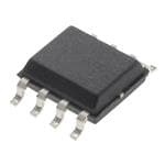
| 描述 | IC OPAMP GP 4MHZ RRO 8SO运算放大器 - 运放 Single Rail-to-Rail |
| 产品分类 | Linear - Amplifiers - Instrumentation, OP Amps, Buffer Amps集成电路 - IC |
| 品牌 | STMicroelectronics |
| 产品手册 | |
| 产品图片 |
|
| rohs | 符合RoHS无铅 / 符合限制有害物质指令(RoHS)规范要求 |
| 产品系列 | 放大器 IC,运算放大器 - 运放,STMicroelectronics TS921IDT- |
| 数据手册 | |
| 产品型号 | TS921IDT |
| 产品目录页面 | |
| 产品种类 | 运算放大器 - 运放 |
| 供应商器件封装 | 8-SO |
| 共模抑制比—最小值 | 60 dB |
| 关闭 | No Shutdown |
| 其它名称 | 497-4074-1 |
| 其它有关文件 | http://www.st.com/web/catalog/sense_power/FM123/SC61/SS1613/LN1590/PF65461?referrer=70071840http://www.st.com/web/catalog/sense_power/FM123/SC61/SS1613/LN1591/PF65461?referrer=70071840 |
| 包装 | 剪切带 (CT) |
| 压摆率 | 1.3 V/µs |
| 商标 | STMicroelectronics |
| 增益带宽生成 | 4 MHz |
| 增益带宽积 | 4MHz |
| 安装类型 | 表面贴装 |
| 安装风格 | SMD/SMT |
| 封装 | Reel |
| 封装/外壳 | 8-SOIC(0.154",3.90mm 宽) |
| 封装/箱体 | SO-8 |
| 工作温度 | -40°C ~ 125°C |
| 工作电源电压 | 2.7 V to 12 V |
| 工厂包装数量 | 2500 |
| 技术 | BiCMOS |
| 放大器类型 | Low Noise Amplifier |
| 最大工作温度 | + 125 C |
| 最小工作温度 | - 40 C |
| 标准包装 | 1 |
| 电压-电源,单/双 (±) | 2.7 V ~ 12 V |
| 电压-输入失调 | 3mV |
| 电流-电源 | 1mA |
| 电流-输入偏置 | 15nA |
| 电流-输出/通道 | 80mA |
| 电源电流 | 1.5 mA |
| 电路数 | 1 |
| 系列 | TS921 |
| 转换速度 | 1.3 V/us |
| 输入偏压电流—最大 | 100 nA |
| 输入参考电压噪声 | 9 nV |
| 输入补偿电压 | 3 mV |
| 输出电流 | 80 mA |
| 输出类型 | 满摆幅 |
| 通道数量 | 1 Channel |


- 商务部:美国ITC正式对集成电路等产品启动337调查
- 曝三星4nm工艺存在良率问题 高通将骁龙8 Gen1或转产台积电
- 太阳诱电将投资9.5亿元在常州建新厂生产MLCC 预计2023年完工
- 英特尔发布欧洲新工厂建设计划 深化IDM 2.0 战略
- 台积电先进制程称霸业界 有大客户加持明年业绩稳了
- 达到5530亿美元!SIA预计今年全球半导体销售额将创下新高
- 英特尔拟将自动驾驶子公司Mobileye上市 估值或超500亿美元
- 三星加码芯片和SET,合并消费电子和移动部门,撤换高东真等 CEO
- 三星电子宣布重大人事变动 还合并消费电子和移动部门
- 海关总署:前11个月进口集成电路产品价值2.52万亿元 增长14.8%


PDF Datasheet 数据手册内容提取
TS921 Rail-to-rail high output current single operational amplifier − Datasheet production data Features ■ Rail-to-rail input and output ■ Low noise: 9 nV/√ Hz N ■ Low distortion DIP8 ■ High output current: 80 mA (able to drive 32 Ω (plastic package) loads) ■ High-speed: 4 MHz, 1 V/μs ■ Operating from 2.7 V to 12 V ■ ESD internal protection: 1.5 kV D SO-8 ■ Latch-up immunity (plastic micropackage) ■ Macromodel included in this specification Applications ■ Headphone amplifier P ■ Piezoelectric speaker driver TSSOP8 (thin shrink small outline package) ■ Sound cards, multimedia systems ■ Line driver, actuator driver ■ Servo amplifier Pin connections (top view) ■ Mobile phone and portable communication sets ■ Instrumentation with low noise as key factor Table 1. Device summary Temperature Order code Package Packing Marking range TS921IN -40 °C, +125 °C DIP8 Tube TS921IN TS921ID/IDT SO-8 Tube or tape and reel 921I TSSOP8 TS921IPT Tape and reel (thin shrink outline package) September 2012 Doc ID 5560 Rev 4 1/16 This is information on a product in full production. www.st.com 16
Description TS921 1 Description The TS921 device is a rail-to-rail single BiCMOS operational amplifier optimized and fully specified for 3 V and 5 V operation. Its high output current allows low load impedances to be driven. The TS921 device exhibits very low noise, low distortion and low offset. It has a high output current capability which makes this device an excellent choice for high quality, low voltage or battery operated audio systems. The device is stable for capacitive loads up to 500 pF. 2/16 Doc ID 5560 Rev 4
TS921 Absolute maximum ratings 2 Absolute maximum ratings Table 2. K ey parameters and their absolute maximum ratings Symbol Parameter Condition Value Unit V Supply voltage(1) 14 V CC V Differential input voltage(2) ±1 V id V Input voltage V - 0.3 to V + 0.3 V i DD CC T Storage temperature -65 to +150 °C stg T Maximum junction temperature 150 °C j SO-8 125 R Thermal resistance junction-to-ambient TSSOP8 120 °C/W thja DIP8 85 SO-8 40 R Thermal resistance junction-to-case TSSOP8 37 °C/W thjc DIP8 41 HBM 1.5 kV Human body model(3) MM ESD Electrostatic discharge 100 V Machine model(4) CDM 1.5 kV Charged device model Output short-circuit duration See(5) Latch-up immunity 200 mA 10 sec., 250 °C standard package Soldering temperature 10 sec., 260 lead-free package 1. All voltage values, except differential voltage are with respect to network ground terminal. 2. Differential voltages are the non-inverting input terminal with respect to the inverting input terminal. If V > ±1 V, the id maximum input current must not exceed ±1 mA. In this case (V > ±1 V) an input serie resistor must be added to limit input id current. 3. Human body model, 100 pF discharged through a 1.5 kΩ resistor into pin of device. 4. Machine model ESD, a 200 pF cap is charged to the specified voltage, then discharged directly into the IC with no external series resistor (internal resistor < 5 Ω), into pin to pin of device. 5. There is no short-circuit protection inside the device: short-circuits from the output to V can cause excessive heating. The CC maximum output current is approximately 80 mA, independent of the magnitude of V . Destructive dissipation can result CC from simultaneous short-circuits on all amplifiers. Table 3. O perating conditions Symbol Parameter Value Unit V Supply voltage 2.7 to 12 V CC V Common mode input voltage range V - 0.2 to V + 0.2 V icm DD CC T Operating free air temperature range -40 to +125 °C oper Doc ID 5560 Rev 4 3/16
Electrical characteristics TS921 3 Electrical characteristics Table 4. E lectrical characteristics for V =3 V, V =0 V, V =V /2, R connected to CC DD icm CC L V /2, T =25 °C (unless otherwise specified) CC amb Symbol Parameter Conditions Min. Typ. Max. Unit V Input offset voltage 3 io mV at T ≤ T ≤ T 5 min. amb max ΔV Input offset voltage drift 2 μV/°C io I Input offset current V =1.5 V 1 30 nA io out I Input bias current V =1.5 V 15 100 nA ib out V High level output voltage R =600 Ω 2.87 OH L V R =32 Ω 2.63 L V Low level output voltage R =600 Ω 100 OL L mV R =32 Ω 180 L A Large signal voltage gain V = 2 V vd out pk-pk R =600 Ω 35 V/mV L R =32 Ω 16 L GBP Gain bandwidth product R = 600 Ω 4 MHz L I Supply current No load, V = V /2 1 1.5 mA CC out CC CMR Common mode rejection ratio 60 80 dB SVR Supply voltage rejection ratio V = 2.7 to 3.3 V 60 80 dB CC I Output short-circuit current 50 80 mA o SR Slew rate 0.7 1.3 V/μs Pm Phase margin at unit gain R = 600 Ω, C =100 pF 68 Degrees L L GM Gain margin R = 600 Ω, C =100 pF 12 dB L L nV e Equivalent input noise voltage f = 1 kHz 9 ------------ n Hz THD Total harmonic distortion V =2 V , f=1 kHz, out pk-pk 0.005 % A =1, R =600 Ω v L 4/16 Doc ID 5560 Rev 4
TS921 Electrical characteristics Table 5. E lectrical characteristics for V = 5 V, V = 0 V, V = V /2, R connected to V /2, CC DD icm CC L CC T = 25 °C (unless otherwise specified) amb Symbol Parameter Conditions Min. Typ. Max. Unit Vio Input offset voltage 3 mV at T ≤ T ≤ T 5 min. amb max ΔVio Input offset voltage drift 2 μV/°C Iio Input offset current Vout = 1.5 V 1 30 nA Iib Input bias current Vout = 1.5 V 15 100 nA V High level output voltage OH 4.85 R = 600 Ω V L 4.4 R = 32 Ω L VOL Low level output voltage RL = 600 Ω 120 mV R = 32 Ω 300 L A Large signal voltage gain V = 2 V vd out pk-pk R = 600 Ω 35 V/mV L R = 32 Ω 16 L GBP Gain bandwidth product RL = 600 Ω 4 MHz I Supply current No load, V = V /2 1 1.5 mA CC out CC CMR Common mode rejection ratio 60 80 dB SVR Supply voltage rejection ratio V = 4.5 to 5.5 V 60 80 dB CC I Output short-circuit current 50 80 mA o SR Slew rate 0.7 1.3 V/μs Pm Phase margin at unit gain R = 600 Ω, C =100 pF 68 Degrees L L GM Gain margin R = 600 Ω, C =100 pF 12 dB L L nV e Equivalent input noise voltage f = 1 kHz 9 ------------ n Hz V = 2 V , f=1 kHz, THD Total harmonic distortion out pk-pk 0.005 % A =1, R =600 Ω v L Doc ID 5560 Rev 4 5/16
Electrical characteristics TS921 Figure 1. Output short-circuit vs. output Figure 2. Voltage gain and phase vs. voltage (V = 5 V, V = 0 V) frequency (R = 10 kΩ, C = 100 pF) CC DD L L 100 60 180 A) 80 Phase m ( 60 nt Sink 40 120 e 40 L rr Gain L uit cu 200 dB) deg.) rc n( 20 60 e( ort-ci --4200 Gai Phas h s ut -60 0 0 p Source ut -80 O -100 -120 -20 -60 0 1 2 3 1E+02 1E+03 1E+04 1E+05 1E+06 1E+07 1E+08 Output voltage(V) Frequency (Hz) Figure 3. Output short-circuit vs. output Figure 4. Equivalent input noise voltage vs. voltage (V = 3 V, V = 0 V) frequency (V = ±1.5 V, R = 100 Ω) CC DD CC L A) 100 z) 30 ort-circuitcurrent(m -22468000000 Sink nputnoise(nV/sqrt(H 11220505 h -40 i s nt utput --8600 Source uivale 5 O q -100 E 0 0 0,5 1 1,5 2 2,5 3 0.01 0.1 1 10 100 Output voltage (V) Frequency(kHz) Figure 5. Output supply current vs. supply Figure 6. THD + noise vs. frequency (R = 2 kΩ, L voltage V = 10 Vpp, V = ±6 V, A = 1) o CC v 0.02 %)0.015 ( e s noi 0.01 + D H T0.005 0 0.01 0.1 1 10 100 Frequency(kHz) 6/16 Doc ID 5560 Rev 4
TS921 Electrical characteristics Figure 7. THD + noise vs. frequency Figure 8. THD + noise vs. output voltage (R = 32 Ω, V = 4 Vpp, (R = 600 Ω, f = 1 kHz, L o L V = ±2.5 V, A = 1) V = 0/3 V, A = -1) CC v CC v 0.04 10 0.032 %) %) 1 ( ( e0.024 e s s oi oi n n THD + 0.016 THD + 0.1 0.008 0 0.01 0.01 0.1 1 10 100 0 0.2 0.4 0.6 0.8 1 Frequency(kHz) Figure 9. THD + noise vs. frequency Figure 10. THD + noise vs. output voltage (R = 32 Ω, V = 2 Vpp, (R = 32 Ω, f = 1 kHz, L o L V = ±1.5 V, A = 10) V = ±1.5 V, A = -1) CC v CC v 10 0.7 0.6 1 %)0.5 %) noise(0.4 noise( 0.1 +0.3 + D D TH0.2 TH 0.01 0.1 0 0.01 0.1 1 10 100 0.001 Frequency(kHz) 0 0.2 0.4 0.6 0.8 1 1.2 Figure 11. THD + noise vs. output voltage Figure 12. Open loop gain and phase (R = 2 kΩ, f = 1 kHz, vs. frequency (C = 500 pF) L L V = ±1.5 V, A = -1) CC v 10,000 50 180 40 1,000 D +noise(%) 0,100 Gain(dB)2300 61020 Phase(deg.) H T 0,010 10 0 0 0,001 1E+2 1E+3 1E+4 1E+5 1E+6 1E+7 1E+8 0 0,2 0,4 0,6 0,8 1 1,2 Frequency(Hz) Doc ID 5560 Rev 4 7/16
Macromodel TS921 4 Macromodel 4.1 Important note concerning this macromodel Please consider following remarks before using this macromodel: ● All models are a trade-off between accuracy and complexity (i.e. simulation time). ● Macromodels are not a substitute to breadboarding; rather, they confirm the validity of a design approach and help to select surrounding component values. ● A macromodel emulates the NOMINAL performance of a TYPICAL device within SPECIFIED OPERATING CONDITIONS (i.e. temperature, supply voltage, etc.). Thus the macromodel is often not as exhaustive as the datasheet, its goal is to illustrate the main parameters of the product. ● Data issued from macromodels used outside of its specified conditions (V , temperature, etc.) or even worse: outside of the device operating conditions CC (V , V , etc.) are not reliable in any way. CC icm In Section4.3, the electrical characteristics resulting from the use of these macromodels are presented. 4.2 Electrical characteristics from macromodelization Table 6. E lectrical characteristics resulting from macromodel simulation at V = 3 V, CC V = 0 V, R , C connected to V , T = 25 °C (unless otherwise specified) DD L L CC/2 amb Symbol Conditions Value Unit V 0 mV io A R = 10 kΩ 200 V/mV vd L I No load, per operator 1.2 mA CC V -0.2 to 3.2 V icm V R = 10 kΩ 2.95 V OH L V R = 10 kΩ 25 mV OL L I V = 3 V 80 mA sink O I V = 0 V 80 mA source O GBP R = 600 kΩ 4 MHz L SR R = 10 kΩ, C = 100 pF 1.3 V/μs L L φm R = 600 kΩ 68 Degrees L 8/16 Doc ID 5560 Rev 4
TS921 Macromodel 4.3 Macromodel code ** Standard Linear Ics Macromodels, 1996. ** CONNECTIONS: * 1 INVERTING INPUT * 2 NON-INVERTING INPUT * 3 OUTPUT * 4 POSITIVE POWER SUPPLY * 5 NEGATIVE POWER SUPPLY .SUBCKT TS921 1 3 2 4 5 (analog) ********************************************************* .MODEL MDTH D IS=1E-8 KF=2.664234E-16 CJO=10F * INPUT STAGE CIP 2 5 1.000000E-12 CIN 1 5 1.000000E-12 EIP 10 5 2 5 1 EIN 16 5 1 5 1 RIP 10 11 8.125000E+00 RIN 15 16 8.125000E+00 RIS 11 15 2.238465E+02 DIP 11 12 MDTH 400E-12 DIN 15 14 MDTH 400E-12 VOFP 12 13 DC 153.5u VOFN 13 14 DC 0 IPOL 13 5 3.200000E-05 CPS 11 15 1e-9 DINN 17 13 MDTH 400E-12 VIN 17 5 -0.100000e+00 DINR 15 18 MDTH 400E-12 VIP 4 18 0.400000E+00 FCP 4 5 VOFP 1.865000E+02 FCN 5 4 VOFN 1.865000E+02 FIBP 2 5 VOFP 6.250000E-03 FIBN 5 1 VOFN 6.250000E-03 * GM1 STAGE *************** FGM1P 119 5 VOFP 1.1 FGM1N 119 5 VOFN 1.1 RAP 119 4 2.6E+06 RAN 119 5 2.6E+06 * GM2 STAGE *************** G2P 19 5 119 5 1.92E-02 G2N 19 5 119 4 1.92E-02 R2P 19 4 1E+07 R2N 19 5 1E+07 ************************** VINT1 500 0 5 Doc ID 5560 Rev 4 9/16
Macromodel TS921 GCONVP 500 501 119 4 19.38!send ds VP, I(VP)=(V119-V4)/2/Ut VP 501 0 0 GCONVN 500 502 119 5 19.38!send ds VN, I(VN)=(V119-V5)/2/Ut VN 502 0 0 ********* orientation isink isource ******* VINT2 503 0 5 FCOPY 503 504 VOUT 1 DCOPYP 504 505 MDTH 400E-9 VCOPYP 505 0 0 DCOPYN 506 504 MDTH 400E-9 VCOPYN 0 506 0 *************************** F2PP 19 5 poly(2) VCOPYP VP 0 0 0 0 0.5!multiply I(vout)*I(VP)=Iout*(V119- V4)/2/Ut F2PN 19 5 poly(2) VCOPYP VN 0 0 0 0 0.5 !multiply I(vout)*I(VN)=Iout*(V119- V5)/2/Ut F2NP 19 5 poly(2) VCOPYN VP 0 0 0 0 1.75 !multiply I(vout)*I(VP)=Iout*(V119- V4)/2/Ut F2NN 19 5 poly(2) VCOPYN VN 0 0 0 0 1.75 !multiply I(vout)*I(VN)=Iout*(V119- V5)/2/Ut * COMPENSATION ************ CC 19 119 25p * OUTPUT*********** DOPM 19 22 MDTH 400E-12 DONM 21 19 MDTH 400E-12 HOPM 22 28 VOUT 6.250000E+02 VIPM 28 4 5.000000E+01 HONM 21 27 VOUT 6.250000E+02 VINM 5 27 5.000000E+01 VOUT 3 23 0 ROUT 23 19 6 COUT 3 5 1.300000E-10 DOP 19 25 MDTH 400E-12 VOP 4 25 1.052 DON 24 19 MDTH 400E-12 VON 24 5 1.052 .ENDS 10/16 Doc ID 5560 Rev 4
TS921 Package information 5 Package information In order to meet environmental requirements, ST offers these devices in different grades of ECOPACK® packages, depending on their level of environmental compliance. ECOPACK specifications, grade definitions and product status are available at: www.st.com. ECOPACK is an ST trademark. Doc ID 5560 Rev 4 11/16
Package information TS921 Figure 13. DIP8 package outline T able 7. DIP8 package mechanical data Dimensions Symbol mm inch Min. Typ. Max. Min. Typ. Max. A 3.3 0.130 a1 0.7 0.028 B 1.39 1.65 0.055 0.065 B1 0.91 1.04 0.036 0.041 b 0.5 0.020 b1 0.38 0.5 0.015 0.020 D 9.8 0.386 E 8.8 0.346 e 2.54 0.100 e3 7.62 0.300 e4 7.62 0.300 F 7.1 0.280 I 4.8 0.189 L 3.3 0.130 Z 0.44 1.6 0.017 0.063 12/16 Doc ID 5560 Rev 4
TS921 Package information Figure 14. SO-8 package outline 0016023/C T able 8. SO-8 package mechanical data Dimensions Symbol mm inch Min. Typ. Max. Min. Typ. Max. A 1.35 1.75 0.053 0.069 A1 0.10 0.25 0.04 0.010 A2 1.10 1.65 0.043 0.065 B 0.33 0.51 0.013 0.020 C 0.19 0.25 0.007 0.010 D 4.80 5.00 0.189 0.197 E 3.80 4.00 0.150 0.157 e 1.27 0.050 H 5.80 6.20 0.228 0.244 h 0.25 0.50 0.010 0.020 L 0.40 1.27 0.016 0.050 k 8° (max.) ddd 0.1 0.04 Doc ID 5560 Rev 4 13/16
Package information TS921 Figure 15. TSSOP8 package outline 0079397/D T able 9. TSSOP8 package mechanical data Dimensions Symbol mm inch Min. Typ. Max. Min. Typ. Max. A 1.2 0.047 A1 0.05 0.15 0.002 0.006 A2 0.80 1.00 1.05 0.031 0.039 0.041 b 0.19 0.30 0.007 0.012 c 0.09 0.20 0.004 0.008 D 2.90 3.00 3.10 0.114 0.118 0.122 E 6.20 6.40 6.60 0.244 0.252 0.260 E1 4.30 4.40 4.50 0.169 0.173 0.177 e 0.65 0.0256 K 0° 8° 0° 8° L 0.45 0.60 0.75 0.018 0.024 0.030 L1 1 0.039 14/16 Doc ID 5560 Rev 4
TS921 Revision history 6 Revision history T able 10. Document revision history Date Revision Changes Feb. 2001 1 Initial release - Product in full production. Modifications on AMR table page 2 (explanation of V and V limits, Dec. 2004 2 id i ESD, MM and CDM values added, Rthja added) The following changes were made in this revision: PPAP references inserted in the datasheet see Table1. Nov. 2005 3 Data in tables Electrical characteristics on page4 reformatted for easier use. Thermal Resistance Junction to Case added in Table2 on page3. Updated Figure on page 1(replaced V - by V ). CC DD Updated (renamed) Table1, removed TS921IYD/IYDT devices from Table1. Moved Description to page 2. 19-Sep-2012 4 Updated Figure1 to Figure4, Figure6 to Figure12 (added conditions to titles). Updated ECOPACK text and reformatted Section5 (added Table7 to Table9, reversed order of figures and tables). Minor corrections throughout document. Doc ID 5560 Rev 4 15/16
TS921 Please Read Carefully: Information in this document is provided solely in connection with ST products. STMicroelectronics NV and its subsidiaries (“ST”) reserve the right to make changes, corrections, modifications or improvements, to this document, and the products and services described herein at any time, without notice. All ST products are sold pursuant to ST’s terms and conditions of sale. Purchasers are solely responsible for the choice, selection and use of the ST products and services described herein, and ST assumes no liability whatsoever relating to the choice, selection or use of the ST products and services described herein. No license, express or implied, by estoppel or otherwise, to any intellectual property rights is granted under this document. If any part of this document refers to any third party products or services it shall not be deemed a license grant by ST for the use of such third party products or services, or any intellectual property contained therein or considered as a warranty covering the use in any manner whatsoever of such third party products or services or any intellectual property contained therein. UNLESS OTHERWISE SET FORTH IN ST’S TERMS AND CONDITIONS OF SALE ST DISCLAIMS ANY EXPRESS OR IMPLIED WARRANTY WITH RESPECT TO THE USE AND/OR SALE OF ST PRODUCTS INCLUDING WITHOUT LIMITATION IMPLIED WARRANTIES OF MERCHANTABILITY, FITNESS FOR A PARTICULAR PURPOSE (AND THEIR EQUIVALENTS UNDER THE LAWS OF ANY JURISDICTION), OR INFRINGEMENT OF ANY PATENT, COPYRIGHT OR OTHER INTELLECTUAL PROPERTY RIGHT. UNLESS EXPRESSLY APPROVED IN WRITING BY TWO AUTHORIZED ST REPRESENTATIVES, ST PRODUCTS ARE NOT RECOMMENDED, AUTHORIZED OR WARRANTED FOR USE IN MILITARY, AIR CRAFT, SPACE, LIFE SAVING, OR LIFE SUSTAINING APPLICATIONS, NOR IN PRODUCTS OR SYSTEMS WHERE FAILURE OR MALFUNCTION MAY RESULT IN PERSONAL INJURY, DEATH, OR SEVERE PROPERTY OR ENVIRONMENTAL DAMAGE. ST PRODUCTS WHICH ARE NOT SPECIFIED AS "AUTOMOTIVE GRADE" MAY ONLY BE USED IN AUTOMOTIVE APPLICATIONS AT USER’S OWN RISK. Resale of ST products with provisions different from the statements and/or technical features set forth in this document shall immediately void any warranty granted by ST for the ST product or service described herein and shall not create or extend in any manner whatsoever, any liability of ST. ST and the ST logo are trademarks or registered trademarks of ST in various countries. Information in this document supersedes and replaces all information previously supplied. The ST logo is a registered trademark of STMicroelectronics. All other names are the property of their respective owners. © 2012 STMicroelectronics - All rights reserved STMicroelectronics group of companies Australia - Belgium - Brazil - Canada - China - Czech Republic - Finland - France - Germany - Hong Kong - India - Israel - Italy - Japan - Malaysia - Malta - Morocco - Philippines - Singapore - Spain - Sweden - Switzerland - United Kingdom - United States of America www.st.com 16/16 Doc ID 5560 Rev 4
Mouser Electronics Authorized Distributor Click to View Pricing, Inventory, Delivery & Lifecycle Information: S TMicroelectronics: TS921ID TS921IN TS921IPT TS921IDT