ICGOO在线商城 > 集成电路(IC) > 线性 - 放大器 - 仪表,运算放大器,缓冲器放大器 > AD8606ARMZ-R7
 Datasheet下载
- 型号: AD8606ARMZ-R7
- 制造商: Analog
- 库位|库存: xxxx|xxxx
- 要求:
| 数量阶梯 | 香港交货 | 国内含税 |
| +xxxx | $xxxx | ¥xxxx |
查看当月历史价格
查看今年历史价格
AD8606ARMZ-R7产品简介:
ICGOO电子元器件商城为您提供AD8606ARMZ-R7由Analog设计生产,在icgoo商城现货销售,并且可以通过原厂、代理商等渠道进行代购。 AD8606ARMZ-R7价格参考。AnalogAD8606ARMZ-R7封装/规格:线性 - 放大器 - 仪表,运算放大器,缓冲器放大器, General Purpose Amplifier 2 Circuit Rail-to-Rail 8-MSOP。您可以下载AD8606ARMZ-R7参考资料、Datasheet数据手册功能说明书,资料中有AD8606ARMZ-R7 详细功能的应用电路图电压和使用方法及教程。
AD8606ARMZ-R7是Analog Devices Inc.推出的一款精密双通道CMOS运算放大器,属于线性放大器类别,广泛应用于对精度、低噪声和低功耗有较高要求的场景。其典型应用场景包括工业控制、传感器信号调理、医疗设备、便携式仪器以及数据采集系统。

该器件具有低失调电压、低输入偏置电流和轨到轨输入输出特性,适合处理微弱信号的放大与调理,例如在压力传感器、热电偶、应变片等传感器接口电路中发挥关键作用。同时,其宽电源电压范围(2.7V至5.5V)和低静态电流使其适用于电池供电设备,如手持式测试仪器和远程监控系统。

在医疗电子中,AD8606ARMZ-R7可用于心电图(ECG)前端放大电路或血糖仪信号处理模块,确保信号的高保真放大。此外,在精密测量仪器和自动测试设备中,其低温漂和高稳定性保障了长期工作的可靠性。

综上,AD8606ARMZ-R7凭借其高精度、低噪声和宽工作电压特性,成为工业、医疗及便携式精密电子设备中的理想选择。
| 参数 | 数值 |
| -3db带宽 | - |
| 产品目录 | 集成电路 (IC)半导体 |
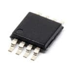
| 描述 | IC OPAMP GP 10MHZ RRO 8MSOP精密放大器 Prec Low Noise CMOS RRIO Dual |
| 产品分类 | Linear - Amplifiers - Instrumentation, OP Amps, Buffer Amps集成电路 - IC |
| 品牌 | Analog Devices |
| 产品手册 | |
| 产品图片 |
|
| rohs | 符合RoHS无铅 / 符合限制有害物质指令(RoHS)规范要求 |
| 产品系列 | 放大器 IC,精密放大器,Analog Devices AD8606ARMZ-R7DigiTrim® |
| 数据手册 | |
| 产品型号 | AD8606ARMZ-R7 |
| 产品培训模块 | http://www.digikey.cn/PTM/IndividualPTM.page?site=cn&lang=zhs&ptm=17027http://www.digikey.cn/PTM/IndividualPTM.page?site=cn&lang=zhs&ptm=30008http://www.digikey.cn/PTM/IndividualPTM.page?site=cn&lang=zhs&ptm=26202 |
| 产品种类 | 精密放大器 |
| 供应商器件封装 | 8-MSOP |
| 共模抑制比—最小值 | 100 dB |
| 关闭 | No |
| 其它名称 | AD8606ARMZ-R7DKR |
| 包装 | Digi-Reel® |
| 压摆率 | 5 V/µs |
| 可用增益调整 | 120 dB |
| 商标 | Analog Devices |
| 增益带宽生成 | 10 MHz |
| 增益带宽积 | 10MHz |
| 安装类型 | 表面贴装 |
| 安装风格 | SMD/SMT |
| 封装 | Reel |
| 封装/外壳 | 8-TSSOP,8-MSOP(0.118",3.00mm 宽) |
| 封装/箱体 | MSOP-8 |
| 工作温度 | -40°C ~ 125°C |
| 工作电源电压 | 2.7 V to 5.5 V |
| 工厂包装数量 | 1000 |
| 放大器类型 | 通用 |
| 最大工作温度 | + 125 C |
| 最小工作温度 | - 40 C |
| 标准包装 | 1 |
| 电压-电源,单/双 (±) | 2.7 V ~ 5.5 V |
| 电压-输入失调 | 80µV |
| 电压增益dB | 120 dB |
| 电流-电源 | 1mA |
| 电流-输入偏置 | 0.2pA |
| 电流-输出/通道 | 80mA |
| 电源电压-最大 | 6 V |
| 电源电压-最小 | 2.7 V |
| 电源电流 | 1.2 mA |
| 电源类型 | Single |
| 电路数 | 2 |
| 系列 | AD8606 |
| 视频文件 | http://www.digikey.cn/classic/video.aspx?PlayerID=1364138032001&width=640&height=505&videoID=2245193153001 |
| 转换速度 | 5 V/us |
| 输入偏压电流—最大 | 1 pA |
| 输入电压范围—最大 | 5.5 V |
| 输入补偿电压 | 20 uV |
| 输出电流 | 80 mA |
| 输出类型 | Rail to Rail Input/Output |
| 通道数量 | 2 Channel |
| 配用 | /product-detail/zh/EVAL-CN0336-PMDZ/EVAL-CN0336-PMDZ-ND/4759176 |


- 商务部:美国ITC正式对集成电路等产品启动337调查
- 曝三星4nm工艺存在良率问题 高通将骁龙8 Gen1或转产台积电
- 太阳诱电将投资9.5亿元在常州建新厂生产MLCC 预计2023年完工
- 英特尔发布欧洲新工厂建设计划 深化IDM 2.0 战略
- 台积电先进制程称霸业界 有大客户加持明年业绩稳了
- 达到5530亿美元!SIA预计今年全球半导体销售额将创下新高
- 英特尔拟将自动驾驶子公司Mobileye上市 估值或超500亿美元
- 三星加码芯片和SET,合并消费电子和移动部门,撤换高东真等 CEO
- 三星电子宣布重大人事变动 还合并消费电子和移动部门
- 海关总署:前11个月进口集成电路产品价值2.52万亿元 增长14.8%


PDF Datasheet 数据手册内容提取
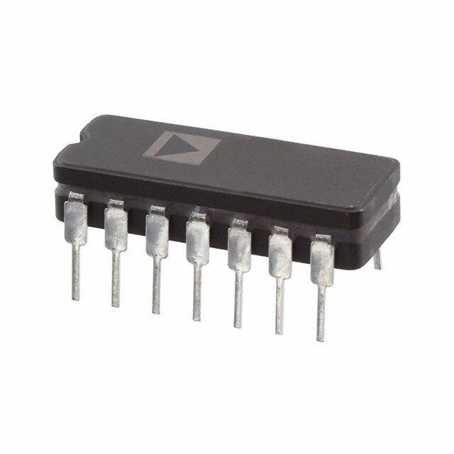
Precision, Low Noise, CMOS, Rail-to-Rail, Input/Output Operational Amplifiers Data Sheet AD8605/AD8606/AD8608 FEATURES PIN CONFIGURATIONS Low offset voltage: 65 μV maximum BALLA1 CORNER Low input bias currents: 1 pA maximum Low noise: 8 nV/√Hz OUTA V+ OUTB Wide bandwidth: 10 MHz A1 A2 A3 High open-loop gain: 1000 V/mV –INA –INB Unity gain stable B1 B3 Single-supply operation: 2.7 V to 5.5 V +INA V– +INB 5-ball WLCSP for single (AD8605) and 8-ball WLCSP for APhPdoPutoaLdlI C(iAoAdDTe8 I6aO0mN6p)S lif ication O+UVINT– 123 (NAToOtD Pto8 V 6SIE0cWa5le) 54 –VI+N02731-001 (CB1ALTALO SDPCID8 V2E6IE 0DW6OWCN3) 02731-057 Battery-powered instrumentation Figure 1. 5-Lead SOT-23 (RJ Suffix) Figure 2. 8-Ball WLCSP (CB Suffix) Multipole filters TOPVIEW Sensors (BUMP SIDE DOWN) OUT A 1 14 OUT D Barcode scanners OUT V+ –IN A 2 13 –IN D Audio 1 5 +IN A 3 AD8608 12 +IN D GENERAL DESCRIPTION V2– V+ 4 (NToOt Pto V SIEcWale) 11 V– +IN –IN +IN B 5 10 +IN C The AD8605, AD8606, and AD86081 are single, dual, and quad 3 4 –IN B 6 9 –IN C rfeaailt-utroe- rvaeirl yin lpowut oafnfsde ot uvotpltuatg, es,i nlogwle -insuppupt lvyo altmagpeli fainedrs c. uTrhreeyn t AD8605 ONLY 02731-006 OUT B 7 8 OUT C02731-004 noise, and wide signal bandwidth. They use the Analog Devices, Figure 3. 5-Ball WLCSP (CB Suffix) Figure 4. 14-Lead SOIC_N (R Suffix) Inc. patented DigiTrim® trimming technique, which achieves superior precision without laser trimming. OUT A 1 14 OUT D Tcwuhidrere ec nvoatmsr,ib eaitnnyda ot hifo iagnph po slfip cloeaewtido o nmfsfas. ekFteisls,t etlohrswe,s ienn oatemisgerp,a lvtifoeirresyr,s lp ouhwsoe tfionudpl uiiontd abe i as O+–UIINNTV AAA– (14NAToOtD Pto8 V 6SIE0cWa6le85) O–+VII+UNNT BB B02731-003 O+–+–UIIIINNNNTV BBBAA+ (7NAToOtD Pto8 V 6SIE0cWa8le8) –+V–O+IIII–UNNNNT DCDC C02731-002 amplifiers, and high impedance sensors all benefit from the Figure 5. 8-Lead MSOP (RM Suffix), Figure 6. 14-Lead TSSOP (RU Suffix) 8-Lead SOIC_N (R Suffix) combination of performance features. Audio and other ac applications benefit from the wide bandwidth and low distortion. Applications for these amplifiers include optical control loops, portable and loop-powered instrumentation, and audio amplification for portable devices. The AD8605, AD8606, and AD8608 are specified over the extended industrial temperature range (−40°C to +125°C). The AD8605 single is available in 5-lead SOT-23 and 5-ball WLCSP packages. The AD8606 dual is available in an 8-lead MSOP, an 8-ball WLSCP, and a narrow SOIC surface-mounted package. The AD8608 quad is available in a 14-lead TSSOP package and a narrow 14-lead SOIC package. The 5-ball and 8-ball WLCSP offer the smallest available footprint for any surface-mounted operational amplifier. The WLCSP, SOT-23, MSOP, and TSSOP versions are available in tape-and-reel only. 1 Protected by U.S. Patent No. 5,969,657. Rev. O Document Feedback Information furnished by Analog Devices is believed to be accurate and reliable. However, no responsibility is assumed by Analog Devices for its use, nor for any infringements of patents or other One Technology Way, P.O. Box 9106, Norwood, MA 02062-9106, U.S.A. rights of third parties that may result from its use. Specifications subject to change without notice. No license is granted by implication or otherwise under any patent or patent rights of Analog Devices. Tel: 781.329.4700 ©2002–2017 Analog Devices, Inc. All rights reserved. Trademarks and registered trademarks are the property of their respective owners. Technical Support www.analog.com
AD8605/AD8606/AD8608 Data Sheet TABLE OF CONTENTS Features .............................................................................................. 1 THD + Noise ............................................................................... 16 Applications ....................................................................................... 1 Total Noise Including Source Resistors ................................... 17 General Description ......................................................................... 1 Channel Separation .................................................................... 17 Pin Configurations ........................................................................... 1 Capacitive Load Drive ............................................................... 17 Revision History ............................................................................... 2 Light Sensitivity .......................................................................... 18 5 V Electrical Specifications ............................................................ 4 WLCSP Assembly Considerations ........................................... 18 2.7 V Electrical Specifications ......................................................... 6 I-V Conversion Applications ........................................................ 19 Absolute Maximum Ratings ............................................................ 8 Photodiode Preamplifier Applications .................................... 19 ESD Caution .................................................................................. 8 Audio and PDA Applications ................................................... 19 Typical Performance Characteristics ............................................. 9 Instrumentation Amplifiers ...................................................... 20 Applications Information .............................................................. 16 DAC Conversion ........................................................................ 20 Output Phase Reversal ............................................................... 16 Outline Dimensions ....................................................................... 21 Maximum Power Dissipation ................................................... 16 Ordering Guide .......................................................................... 24 Input Overvoltage Protection ................................................... 16 REVISION HISTORY 11/2017—Rev. N to Rev. O 9/2008—Rev. H to Rev. I Added Figure 44 and Figure 45; Renumbered Sequentially ..... 15 Changes to Input Overvoltage Protection Section..................... 15 Changes to Figure 51 ...................................................................... 17 Changes to Ordering Guide .......................................................... 22 Changes to Ordering Guide .......................................................... 24 2/2008—Rev. G to Rev. H 4/2013—Rev. M to Rev. N Changes to Features .......................................................................... 1 Changes to Input Overvoltage Section and THD + Noise Changes to Table 1 ............................................................................. 4 Section .............................................................................................. 16 Changes to Table 2 ............................................................................. 6 Changes to Total Noise Including Source Resistors Section .......... 17 Changes to Figure 11 ......................................................................... 9 Updated Outline Dimensions ....................................................... 24 Changes to Figure 13, Figure 14, and Figure 16 Captions ........ 10 Changes to Figure 15, Figure 17, and Figure 18 ......................... 10 2/2013—Rev. L to Rev. M Changes to Figure 34 and Figure 35 Captions ............................ 13 Updated Outline Dimensions ....................................................... 21 Changes to Figure 36 ...................................................................... 13 Changes to Ordering Guide .......................................................... 24 Changes to Figure 37 Caption ...................................................... 14 Changes to Figure 38 and Figure 41 ............................................ 14 2/2012—Rev. K to Rev. L Changes to Figure 45 ...................................................................... 15 Changed Functional Block Diagrams Section to Pin Changes to Audio and PDA Applications Section ..................... 18 Configuration Section ...................................................................... 1 Changes to Figure 52 ...................................................................... 18 Changes to Figure 11 ........................................................................ 9 Changes to Ordering Guide .......................................................... 22 Added Figure 33 .............................................................................. 13 10/2007—Rev. F to Rev. G 8/2011—Rev. J to Rev. K Changes to Figure 2 ........................................................................... 1 Changes to Figure 20 ........................................................................ 2 Updated Outline Dimensions ....................................................... 20 Updated Outline Dimensions ....................................................... 20 Changes to Ordering Guide .......................................................... 23 8/2007—Rev. E to Rev. F Added 8-Ball WLCSP Package ......................................... Universal 8/2010—Rev. I to Rev. J Changes to Features .......................................................................... 1 Changes to Figure 10 and Figure 11 ............................................... 9 Changes to Table 1 ............................................................................. 3 Changes to Figure 15 ...................................................................... 10 Changes to Table 2 ............................................................................. 5 Changes to Figure 36 ...................................................................... 13 Changes to Table 4 ............................................................................. 7 Changes to Figure 42 ...................................................................... 14 Updated Outline Dimensions ....................................................... 19 Updated Outline Dimensions ....................................................... 20 Changes to Ordering Guide .......................................................... 21 Changes to Ordering Guide .......................................................... 23 Rev. O | Page 2 of 24
Data Sheet AD8605/AD8606/AD8608 1/2006—Rev. D to Rev. E Added New Figure 8; Renumbered Subsequently ...................... 13 Changes to Table 1 ............................................................................ 3 Added New MicroCSP Assembly Considerations Section ........ 13 Changes to Table 2 ............................................................................ 5 Changes to Figure 9 ........................................................................ 13 Changes to Table 4 ............................................................................ 6 Change to Equation in Photodiode Preamplifier Changes to Figure 12 Caption ......................................................... 8 Applications Section ...................................................................... 13 Changes to Figure 26 and Figure 27 Captions............................. 11 Changes to Figure 12 ...................................................................... 14 Changes to Figure 33 Caption ....................................................... 12 Change to Equation in D/A Conversion Section ........................ 14 Changes to Figure 44 ...................................................................... 14 Updated Outline Dimensions ....................................................... 15 Updated Outline Dimensions ........................................................ 19 Changes to Ordering Guide ........................................................... 20 3/2003—Rev. A to Rev. B Changes to Functional Block Diagram .......................................... 1 5/2004—Rev. C to Rev. D Changes to Absolute Maximum Ratings........................................ 4 Updated Format.................................................................. Universal Changes to Ordering Guide ........................................................... 4 Edit to Light Sensitivity Section .................................................... 16 Changes to Figure 9 ....................................................................... 13 Updated Outline Dimensions ........................................................ 19 Updated Outline Dimensions........................................................ 15 Changes to Ordering Guide ........................................................... 20 11/2002—Rev. 0 to Rev. A 7/2003—Rev. B to Rev. C Change to Electrical Characteristics ............................................... 2 Changes to Features .......................................................................... 1 Changes to Absolute Maximum Ratings........................................ 4 Change to General Description ....................................................... 1 Changes to Ordering Guide ............................................................ 4 Addition to Functional Block Diagrams ........................................ 1 Change to TPC 6 .............................................................................. 5 Addition to Absolute Maximum Ratings ....................................... 4 Updated Outline Dimensions........................................................ 15 Addition to Ordering Guide ............................................................ 4 Change to Equation in Maximum Power Dissipation Section ...... 11 5/2002—Revision 0: Initial Version Added Light Sensitivity Section .................................................... 12 Rev. O | Page 3 of 24
AD8605/AD8606/AD8608 Data Sheet 5 V ELECTRICAL SPECIFICATIONS V = 5 V, V = V/2, T = 25°C, unless otherwise noted. S CM S A Table 1. Parameter Symbol Conditions Min Typ Max Unit INPUT CHARACTERISTICS Offset Voltage V OS AD8605/AD8606 (Except WLCSP) V = 3.5 V, V = 3 V 20 65 µV S CM AD8608 V = 3.5 V, V = 2.7 V 20 75 µV S CM AD8605/AD8606/AD8608 V = 5 V, V = 0 V to 5 V 80 300 µV S CM −40°C < T < +125°C 750 µV A Input Bias Current I 0.2 1 pA B AD8605/AD8606 −40°C < T < +85°C 50 pA A AD8605/AD8606 −40°C < T < +125°C 250 pA A AD8608 −40°C < T < +85°C 100 pA A AD8608 −40°C < T < +125°C 300 pA A Input Offset Current I 0.1 0.5 pA OS −40°C < T < +85°C 20 pA A −40°C < T < +125°C 75 pA A Input Voltage Range 0 5 V Common-Mode Rejection Ratio CMRR V = 0 V to 5 V 85 100 dB CM −40°C < T < +125°C 75 90 dB A Large Signal Voltage Gain A R = 2 kΩ, V = 0.5 V to 4.5 V 300 1000 V/mV VO L O Offset Voltage Drift AD8605/AD8606 ΔV /ΔT −40°C < T < +125°C 1 4.5 µV/°C OS A AD8608 ΔV /ΔT −40°C < T < +125°C 1.5 6.0 µV/°C OS A INPUT CAPACITANCE Common-Mode Input Capacitance C 8.8 pF COM Differential Input Capacitance C 2.6 pF DIFF OUTPUT CHARACTERISTICS Output Voltage High V I = 1 mA 4.96 4.98 V OH L I = 10 mA 4.7 4.79 V L −40°C < T < +125°C 4.6 V A Output Voltage Low V I = 1 mA 20 40 mV OL L I= 10 mA 170 210 mV L −40°C < T < +125°C 290 mV A Output Current I ±80 mA OUT Closed-Loop Output Impedance Z f = 1 MHz, A = 1 1 Ω OUT V POWER SUPPLY Power Supply Rejection Ratio PSRR AD8605/AD8606 V = 2.7 V to 5.5 V 80 95 dB S AD8605/AD8606 WLCSP V = 2.7 V to 5.5 V 75 92 dB S AD8608 V = 2.7 V to 5.5 V 77 92 dB S −40°C < T < +125°C 70 90 dB A Supply Current/Amplifier I I = 0 mA 1 1.2 mA SY OUT −40°C < T < +125°C 1.4 mA A DYNAMIC PERFORMANCE Slew Rate SR R = 2 kΩ, C = 16 pF 5 V/µs L L Settling Time t To 0.01%, 0 V to 2 V step, A = 1 <1 µs S V Unity Gain Bandwidth Product GBP 10 MHz Phase Margin Φ 65 Degrees M Rev. O | Page 4 of 24
Data Sheet AD8605/AD8606/AD8608 Parameter Symbol Conditions Min Typ Max Unit NOISE PERFORMANCE Peak-to-Peak Noise e p-p f = 0.1 Hz to 10 Hz 2.3 3.5 µV p-p n Voltage Noise Density e f = 1 kHz 8 12 nV/√Hz n e f = 10 kHz 6.5 nV/√Hz n Current Noise Density i f = 1 kHz 0.01 pA/√Hz n Rev. O | Page 5 of 24
AD8605/AD8606/AD8608 Data Sheet 2.7 V ELECTRICAL SPECIFICATIONS V = 2.7 V, V = V/2, T = 25°C, unless otherwise noted. S CM S A Table 2. Parameter Symbol Conditions Min Typ Max Unit INPUT CHARACTERISTICS Offset Voltage V OS AD8605/AD8606 (Except WLCSP) V = 3.5 V, V = 3 V 20 65 µV S CM AD8608 V = 3.5 V, V = 2.7 V 20 75 µV S CM AD8605/AD8606/AD8608 V = 2.7 V, V = 0 V to 2.7 V 80 300 µV S CM −40°C < T < +125°C 750 µV A Input Bias Current I 0.2 1 pA B AD8605/AD8606 −40°C < T < +85°C 50 pA A AD8605/AD8606 −40°C < T < +125°C 250 pA A AD8608 −40°C < T < +85°C 100 pA A AD8608 −40°C < T < +125°C 300 pA A Input Offset Current I 0.1 0.5 pA OS −40°C < T < +85°C 20 pA A −40°C < T < +125°C 75 pA A Input Voltage Range 0 2.7 V Common-Mode Rejection Ratio CMRR V = 0 V to 2.7 V 80 95 dB CM −40°C < T < +125°C 70 85 dB A Large Signal Voltage Gain A R = 2 kΩ, V = 0.5 V to 2.2 V 110 350 V/mV VO L O Offset Voltage Drift AD8605/AD8606 ΔV /ΔT −40°C < T < +125°C 1 4.5 µV/°C OS A AD8608 ΔV /ΔT −40°C < T < +125°C 1.5 6.0 µV/°C OS A INPUT CAPACITANCE Common-Mode Input Capacitance C 8.8 pF COM Differential Input Capacitance C 2.6 pF DIFF OUTPUT CHARACTERISTICS Output Voltage High V I = 1 mA 2.6 2.66 V OH L −40°C < T < +125°C 2.6 V A Output Voltage Low V I = 1 mA 25 40 mV OL L −40°C < T < +125°C 50 mV A Output Current I ±30 mA OUT Closed-Loop Output Impedance Z f = 1 MHz, A = 1 1.2 Ω OUT V POWER SUPPLY Power Supply Rejection Ratio PSRR AD8605/AD8606 V = 2.7 V to 5.5 V 80 95 dB S AD8605/AD8606 WLCSP V = 2.7 V to 5.5 V 75 92 dB S AD8608 V = 2.7 V to 5.5 V 77 92 dB S −40°C < T < +125°C 70 90 dB A Supply Current/Amplifier I I = 0 mA 1.15 1.4 mA SY OUT −40°C < T < +125°C 1.5 mA A DYNAMIC PERFORMANCE Slew Rate SR R = 2 kΩ, C = 16 pF 5 V/µs L L Settling Time t To 0.01%, 0 V to 1 V step, A = 1 <0.5 µs S V Unity Gain Bandwidth Product GBP 9 MHz Phase Margin Φ 50 Degrees M Rev. O | Page 6 of 24
Data Sheet AD8605/AD8606/AD8608 Parameter Symbol Conditions Min Typ Max Unit NOISE PERFORMANCE Peak-to-Peak Noise e p-p f = 0.1 Hz to 10 Hz 2.3 3.5 µV p-p n Voltage Noise Density e f = 1 kHz 8 12 nV/√Hz n e f = 10 kHz 6.5 nV/√Hz n Current Noise Density i f = 1 kHz 0.01 pA/√Hz n Rev. O | Page 7 of 24
AD8605/AD8606/AD8608 Data Sheet ABSOLUTE MAXIMUM RATINGS Table 3. Table 4. Parameter Rating Package Type θ 1 θ Unit JA JC Supply Voltage 6 V 5-Ball WLCSP (CB) 170 °C/W Input Voltage GND to VS 5-Lead SOT-23 (RJ) 240 92 °C/W Differential Input Voltage 6 V 8-Ball WLCSP (CB) 115 °C/W Output Short-Circuit Duration to GND Observe Derating Curves 8-Lead MSOP (RM) 206 44 °C/W Storage Temperature Range 8-Lead SOIC_N (R) 157 56 °C/W All Packages −65°C to +150°C 14-Lead SOIC_N (R) 105 36 °C/W Operating Temperature Range 14-Lead TSSOP (RU) 148 23 °C/W All Packages −40°C to +125°C 1 θJA is specified for the worst-case conditions, that is, a device soldered in a Junction Temperature Range circuit board for surface-mount packages. All Packages −65°C to +150°C Lead Temperature (Soldering, 60 sec) 300°C ESD CAUTION Stresses at or above those listed under Absolute Maximum Ratings may cause permanent damage to the product. This is a stress rating only; functional operation of the product at these or any other conditions above those indicated in the operational section of this specification is not implied. Operation beyond the maximum operating conditions for extended periods may affect product reliability. Rev. O | Page 8 of 24
Data Sheet AD8605/AD8606/AD8608 TYPICAL PERFORMANCE CHARACTERISTICS 4500 0.30 VS = 5V 0.25 VS = 5V 4000 TA = 25°C VCM = 0VTO 5V 0.20 3500 S 0.15 R E3000 0.10 FI MPLI2500 mV) 0.05 R OFA2000 V(OS–0.050 E B1500 –0.10 M U N1000 –0.15 –0.20 5000 02731-007 ––00..3205 02731-010 –300 –200 –100 0 100 200 300 0 0.5 1.0 1.5 2.0 2.5 3.0 3.5 4.0 4.5 5.0 OFFSET VOLTAGE (µV) VCM(V) Figure 7. Input Offset Voltage Distribution Figure 10. Input Offset Voltage vs. Common-Mode Voltage (200 Units, 5 Wafer Lots, Including Process Skews) 24 250 VS = 5V VSY = 5V TA = –40°CTO +125°C 200 VCM = VSY/2 20 VCM = 2.5V S A) 150 R p LIFIE16 ENT ( 100 P R M R OFA12 S CU 50 ER BIA 0 MB 8 UT U P N N –50 I 4 AD8605 00 0.4 0.8 1.2 1.6 T2C.V0OS2 .(4µV/2°C.8) 3.2 3.6 4.0 4.4 4.8800-13720 ––115000–50 –25 0 TEM2P5ERATUR5E0 (°C) 75 AA10DD088660068 125 02731-011 Figure 8. AD8608 Input Offset Voltage Drift Distribution Figure 11. Input Bias Current vs. Temperature 20 1k VS = 5V VS = 5V 18 TVAC M= =– 420.5°CVTO +125°C mV) TA = 25°C MPLIFIERS111264 N VOLTAGE (100 OFA10 ATIO 10 BER 8 ATUR SOURCE SINK M S U 6 T N U 1 P 4 T U 02 02731-009 O 0.1 02731-012 0 0.2 0.4 0.6 0.8 1.0 1.2 1.4 1.6 1.8 2.0 2.2 2.4 2.6 0.001 0.01 0.1 1 10 TCVOS (µV/°C) LOAD CURRENT (mA) Figure 9. AD8605/AD8606 Input Offset Voltage Drift Distribution Figure 12. Output Saturation Voltage vs. Load Current Rev. O | Page 9 of 24
AD8605/AD8606/AD8608 Data Sheet 5.00 6 VOH @ 1mA LOAD 4.95 5 OLTAGE (V) 44..8950 VS = 5V WING (V p-p) 43 RVVTASILN ==== 25245Vk.°Ω9CV p-p OUTPUT V 4.80 OUTPUT S 2 AV = 1 VOH @ 10mA LOAD 4.75 1 4.70 02731-013 0 02731-016 –40 –25 –10 5 20 35 50 65 80 95 110 125 1k 10k 100k 1M 10M TEMPERATURE (°C) FREQUENCY (Hz) Figure 13. Output Voltage Swing High vs. Temperature Figure 16. Closed-Loop Output Voltage Swing (FPBW) 0.25 100 VS = 5V VS = 5V VOL @ 10mA LOAD 90 0.20 80 E (V) CE (Ω)70 AV = 100 AG 0.15 AN60 T D OL PE50 PUT V 0.10 UT IM40 AV = 10 AV = 1 T P U T O U30 O 0.05 20 0 VOL @ 1mA LOAD 02731-014 100 02731-017 –40 –25 –10 5 20 35 50 65 80 95 110 125 1k 10k 100k 1M 10M 100M TEMPERATURE (°C) FREQUENCY (Hz) Figure 14. Output Voltage Swing Low vs. Temperature Figure 17. Output Impedance vs. Frequency 100 225 120 VS = ±2.5V VS = 5V 80 RL = 2kΩ 180 110 CL = 20pF 60 PHASE ΦM = 64° 135 100 40 90 90 s) GAIN (dB)–22000 GAIN 40–545ASE (Degree CMRR (dB)876000 H P –40 –90 50 –60 –135 40 –1–0800 ––128205 02731-015 2300 02731-018 10k 100k 1M 10M 40M 1k 10k 100k 1M 10M FREQUENCY (Hz) FREQUENCY (Hz) Figure 15. Open-Loop Gain and Phase vs. Frequency Figure 18. Common-Mode Rejection Ratio (CMRR) vs. Frequency Rev. O | Page 10 of 24
Data Sheet AD8605/AD8606/AD8608 140 1.0 VS = 5V 120 0.9 A) 100 m0.8 R ( 80 FIE0.7 LI B) 60 MP0.6 d A PSRR ( 4200 RRENT/00..45 U C 0 Y 0.3 L P –20 UP0.2 S ––6400 02731-019 0.01 02731-022 1k 10k 100k 1M 10M 0 0.5 1.0 1.5 2.0 2.5 3.0 3.5 4.0 4.5 5.0 FREQUENCY (Hz) SUPPLY VOLTAGE (V) Figure 19. PSRR vs. Frequency Figure 22. Supply Current/Amplifier vs. Supply Voltage 45 40 RVSL == ∞5V VS = 5V %) TA = 25°C OT (35 AV = –1 V) VERSHO3205 E (1µV/DI L O +OS OIS A20 N SIGN15 –OS AGE MALL 10 VOLT S 0510 100 1k02731-020 02731-023 CAPACITANCE (pF) TIME (1s/DIV) Figure 20. Small Signal Overshoot vs. Load Capacitance Figure 23. 0.1 Hz to 10 Hz Input Voltage Noise 2.0 VS = ±2.5V A) RL = 10kΩ m CL = 200pF R ( 1.5 AV = 1 E FI V) LI DI RENT/AMP 1.0 VS = 2.7V VS = 5V GE (50mV/ CUR OLTA Y V PL 0.5 P U S 0 02731-021 02731-024 –40 –25 –10 5 20 35 50 65 80 95 110 125 TIME (200ns/DIV) TEMPERATURE (°C) Figure 21. Supply Current/Amplifier vs. Temperature Figure 24. Small Signal Transient Response Rev. O | Page 11 of 24
AD8605/AD8606/AD8608 Data Sheet 36 VS = ±2.5V VS = ±2.5V RL = 10kΩ 32 CL = 200pF Hz) AV = 1 V/28 n V) Y ( V/DI NSIT24 GE (1 E DE20 A S OLT NOI16 V E G TA12 L O V 02731-025 48 02731-028 TIME (400ns/DIV) 0 0.1 0.2 0.3 0.4 0.5 0.6 0.7 0.8 0.9 1.0 FREQUENCY (kHz) Figure 25. Large Signal Transient Response Figure 28. Voltage Noise Density vs. Frequency 53.6 VS = ±2.5V VS = ±2.5V VOUT 2.5V RVAILVN === 1–5010k0mΩ0V V/ Hz)4406..29 n Y ( 0V SIT33.5 N E 0V E D26.8 S OI N20.1 E G VIN LTA13.4 –50mV O V 02731-026 6.70 02731-029 TIME (400ns/DIV) 0 1 2 3 4 5 6 7 8 9 10 FREQUENCY (kHz) Figure 26. Positive Overload Recovery Figure 29. Voltage Noise Density vs. Frequency 119.2 VS = ±2.5V VS = ±2.5V RL = 10kΩ 104.3 0V AV = –100 Hz) VIN = 50mV V/ 89.4 n Y ( –2.5V SIT 74.5 N 50mV E DE 59.6 S OI N 44.7 E G 0V TA 29.8 L O V 02731-027 14.90 02731-030 TIME (1µs/DIV) 0 10 20 30 40 50 60 70 80 90 100 FREQUENCY (Hz) Figure 27. Negative Overload Recovery Figure 30. Voltage Noise Density vs. Frequency Rev. O | Page 12 of 24
Data Sheet AD8605/AD8606/AD8608 1800 1k VS = 2.7V VS = 2.7V 1600 VTAC M= =2 50°VCTO 2.7V mV) TA = 25°C MPLIFIERS111204000000 N VOLTAGE (100 SOURCE R OFA 800 URATIO 10 SINK MBE 600 SAT U T N U 1 400 P T U 2000 02731-031 O0.1 02731-033 –300 –200 –100 0 100 200 300 0.001 0.01 0.1 1 10 OFFSET VOLTAGE (µV) LOAD CURRENT (mA) Figure 31. Input Offset Voltage Distribution Figure 34. Output Saturation Voltage vs. Load Current 300 2.680 VS = 2.7V VS = 2.7V TA = 25°C 200 2.675 V) µ LTAGE ( 100 AGE (V)2.670 O T SET V 0 T VOL2.665 FF PU VOH @ 1mA LOAD O T UT –100 OU2.660 P N I –200 2.655 –300 02731-032 2.650 02731-034 0 0 0.9 1.8 2.7 –40 –25 –10 5 20 35 50 65 80 95 110 125 COMMON-MODE VOLTAGE (V) TEMPERATURE (°C) Figure 32. Input Offset Voltage vs. Common-Mode Voltage Figure 35. Output Voltage Swing High vs. Temperature (200 Units, 5 Wafer Lots, Including Process Skews) 250 0.045 200 VVSCYM == 2V.S7YV/2 0.040 VS = 2.7V A) 150 0.035 p CURRENT ( 10500 OLTAGE (V)00..002350 VOL @ 1mA LOAD AS T V0.020 UT BI 0 UTPU0.015 P O N –50 I 0.010 AD8605 ––115000–50 –25 0 TEM2P5ERATUR5E0 (°C) 75 AA10DD088660068 125 02731-039 0.0050–40 –25 –10 5TEM2P0ERA3T5URE5 0(°C)65 80 95 110 12502731-035 Figure 33. Input Bias Current vs. Temperature Figure 36. Output Voltage Swing Low vs. Temperature Rev. O | Page 13 of 24
AD8605/AD8606/AD8608 Data Sheet 100 225 60 VS = 2.7V VS = 2.7V 80 RL = 2kΩ 180 TA = 25°C 60 PHASE ΦCLM = = 2 502p.F5° 135 T (%)50 AV = 1 O 40 90 es) SHO40 GAIN (dB)–22000 GAIN 40–545 PHASE (Degre SIGNAL OVER3200 –OS +OS –40 –90 L L A M –60 –135 S10 –1–0800 ––128205 02731-036 0 02731-039 10k 100k 1M 10M 40M 10 100 1k FREQUENCY (Hz) CAPACITANCE (pF) Figure 37. Open-Loop Gain and Phase vs. Frequency Figure 40. Small Signal Overshoot vs. Load Capacitance 3.0 VS = 2.7V 2.5 p) VS = 2.7V DIV) NG (V p- 2.0 RVTAILN === 2225k.°Ω6CV p-p SE (1µV/ WI 1.5 AV = 1 OI S N T E U G P A OUT 1.0 OLT V 0.5 0 02731-037 02731-040 1k 10k 100k 1M 10M TIME (1s/DIV) FREQUENCY (Hz) Figure 38. Closed-Loop Output Voltage Swing vs. Frequency (FPBW) Figure 41. 0.1 Hz to 10 Hz Input Voltage Noise 100 90 VS = 2.7V VS = ±1.35V RL = 10kΩ 80 CL = 200pF Ω) AV = 1 ANCE (7600 AV = 100 mV/DIV) D 0 E 5 MP50 AV = 10 E ( OUTPUT I3400 AV = 1 VOLTAG 20 100 02731-038 02731-041 1k 10k 100k 1M 10M 100M TIME (200ns/DIV) FREQUENCY (Hz) Figure 39. Output Impedance vs. Frequency Figure 42. Small Signal Transient Response Rev. O | Page 14 of 24
Data Sheet AD8605/AD8606/AD8608 5 VS = ±1.35V RL = 10kΩ CL = 200pF 3 AV = 1 DIV) pA) mV/ NT ( 1 E (500 URRE G C OLTA BIAS –1 V –3 TIME (400ns/DIV) 02731-042 –5–2 0COMMON-MOD2E VOLTAGE (V)4 6 02731-145 Figure 43. Large Signal Transient Response Figure 45. Noninverting Input Bias Current vs Common-Mode Voltage 5 3 A) p T ( 1 N E R R U C S –1 A BI –3 –5–2 0COMMON-MOD2E VOLTAGE (V)4 6 02731-144 Figure 44. Inverting Input Bias Current vs Common-Mode Voltage Rev. O | Page 15 of 24
AD8605/AD8606/AD8608 Data Sheet APPLICATIONS INFORMATION OUTPUT PHASE REVERSAL VS = ±2.5V Pthhea asem rpelvifeiresra wl ihs edne fai nveodlt aags ea tchhaat negxec eined pso tlhaer imty aaxti mthue mou itnppuut to f VAIVN == 16V p-p VOUT RL = 10kΩ common-mode voltage drives the input. V) Phase reversal can cause permanent damage to the amplifier; it DI 2V/ VIN can also cause system lockups in feedback loops. The AD8605 E ( G does not exhibit phase reversal even for inputs exceeding the A T L supply voltage by more than 2 V. O V MAXIMUM POWER DISSIPATION Pinocwreears dei, swsihpiacthe dc ainn aanff eIcCt cthaue sbeesh tahvei odri eo tfe tmhep IeCra atunrde tthoe 02731-043 application circuit performance. TIME (4µs/DIV) The absolute maximum junction temperature of the AD8605/ Figure 46. No Phase Reversal AD8606/AD8608 is 150°C. Exceeding this temperature could 1.8 damage or destroy the device. 1.7 1.6 SOIC-14 The maximum power dissipation of the amplifier is calculated 1.5 accorPdDinISgS t=o TJθ−JATA SSIPATION (W)111011......031942 SOTICS-S8OP-14 DI0.8 where: ER 0.7 W0.6 MSOP-8 TJ is the junction temperature. PO0.5 WLCSP-5 T is the ambient temperature. 0.4 A 0.3 FθJiAg uisr eth 4e7 j uconmctipoanr-etso t-haem mbiaexnitm thuemrm poalw reers idsitsasnipcea.t ion with 00..102 5-LEAD SOT-23 02731-044 –45 –20 5 30 55 80 105 130 temperature for the various AD860x family packages. AMBIENT TEMPERATURE (°C) INPUT OVERVOLTAGE PROTECTION Figure 47. Maximum Power Dissipation vs. Ambient Temperature The AD860x has internal protective circuitry. However, if the 0.1 VSY = ±2.5V voltage applied at either input exceeds the supplies by more AV = 1 than 0.5 V, external resistors should be placed in series with BW = 80kHz the inputs. The resistor values can be determined by %)0.01 VIN −VS ≤ 5mA SE ( R OI S + N D The remarkable low input offset current of the AD860x (<1 pA) H T 0.001 allows the use of larger value resistors. With a 10 kΩ resistor at the input, the output voltage has less than 10 nV of error voltage. Aro o1m0 k tΩem rpeseirsatoturr he.a s less than 13 nV/√Hz of thermal noise at 0.0001 02731-045 THD + NOISE 20 100 1k 10k 20k FREQUENCY (Hz) Total harmonic distortion is the ratio of the input signal in V rms Figure 48. THD + Noise vs. Frequency to the total harmonics in V rms throughout the spectrum. Harmonic distortion adds errors to precision measurements and adds unpleasant sonic artifacts to audio systems. The AD860x has a low total harmonic distortion. Figure 48 shows that the AD8605 has less than 0.005% or −86 dB of THD + N over the entire audio frequency range. The AD8605 is configured in positive unity gain, which is the worst case, and with a load of 10 kΩ. Rev. O | Page 16 of 24
Data Sheet AD8605/AD8606/AD8608 TOTAL NOISE INCLUDING SOURCE RESISTORS A snubber network, shown in Figure 51, helps reduce the signal overshoot to a minimum and maintain stability. Although this The low input current noise and input bias current of the circuit does not recover the loss of bandwidth induced by large AD860x make it the ideal amplifier for circuits with substantial capacitive loads, it greatly reduces the overshoot and ringing. input source resistance, such as photodiodes. Input offset voltage This method does not reduce the maximum output swing of the increases by less than 0.5 nV per 1 kΩ of source resistance at amplifier. room temperature and increases to 10 nV at 85°C. The total noise density of the circuit is 0 en,TOTAL = en2+(inRS)2+4kTRS N (dB) ––2400 where: O TI –60 A en is the input voltage noise density of the AD860x. AR P –80 in is the input current noise density of the AD860x. SE RS is the source resistance at the noninverting terminal. EL –100 N k is Boltzmann’s constant (1.38 × 10⁻²³ J/K). HAN–120 T is the ambient temperature in Kelvin (T = 273 + °C). C –140 For example, with R = 10 kΩ, the total voltage noise density is S roughly 15 nV/√Hz. ––116800 02731-046 For RS < 3.9 kΩ, en dominates and en, TOTAL ≈ en. 100 1k 10k 100k 1M 10M 100M FREQUENCY (Hz) The current noise of the AD860x is so low that its total density Figure 49. Channel Separation vs. Frequency does not become a significant term unless R is greater than 6 MΩ. S The total equivalent rms noise over a specific bandwidth is expressed as ( ) VS = ±2.5V E = e BW AV = 1 n n,TOTAL RL = 10kΩ CL = 1000pF where BW is the bandwidth in hertz. V) DI V/ Note that the previous analysis is valid for frequencies greater m 0 than 100 Hz and assumes relatively flat noise, above 10 kHz. For 10 E ( lower frequencies, flicker noise (1/f) must be considered. G A T L CHANNEL SEPARATION O V Channel separation, or inverse crosstalk, is a measure of the signal fTehede AfrDom86 o0n6e h aams ap lcihfiaenr n(cehl asenpnaerla) ttioo na noof tghreera toenr tthhea ns a−m1e6 0I Cd.B 02731-047 TIME (10µs/DIV) up to frequencies of 1 MHz, allowing the two amplifiers to Figure 50. AD8606 Capacitive Load Drive Without Snubber amplify ac signals independently in most applications. CAPACITIVE LOAD DRIVE V+ The AD860x can drive large capacitive loads without oscillation. Figure 50 shows the output of the AD8606 in response to a 200 mV input signal. In this case, the amplifier is configured 4 2 in positive unity gain, worst case for stability, while driving a 200mV 1 1000 pF load at its output. Driving larger capacitive loads in AD8606 VIN 3 unity gain can require the use of additional circuitry. RS RL CL 8V– CS 02731-049 Figure 51. Snubber Network Configuration Rev. O | Page 17 of 24
AD8605/AD8606/AD8608 Data Sheet Figure 52 shows a scope of the output at the snubber circuit. 5000 The overshoot is reduced from over 70% to less than 5%, and 4500 the ringing is eliminated by the snubber. Optimum values for RS 4000 and CS are determined experimentally. NT (pA)3500 3mW/cm2 VS = ±2.5V RRE3000 AV = 1 CU2500 RL = 10kΩ S 2mW/cm2 RS = 90Ω BIA2000 DIV) CCLS == 1700000ppFF PUT 1500 mV/ IN1000 0 LTAGE (10 5000 1mW/cm2 02731-050 O 350 450 550 650 750 850 V WAVELENGTH (nm) Figure 53. AD8605ACB Input Bias Current Response to Direct Illumination of 02731-048 When the WLCSPV paaryciknagg Inet iesn asistsye amndb Wledav oelne ntghteh board with the TIME (10µs/DIV) bump side of the die facing the PCB, reflected light from the Figure 52. Capacitive Load Drive with Snubber PCB surface is incident on active silicon circuit areas and results Table 5 summarizes a few optimum values for capacitive loads. in the increased IB. No performance degradation occurs due to illumination of the backside (substrate) of the AD8605ACB. Table 5. The AD8605ACB is particularly sensitive to incident light with CL (pF) RS (Ω) CS (pF) wavelengths in the near infrared range (NIR, 700 nm to 1000 nm). 500 100 1000 Photons in this waveband have a longer wavelength and lower 1000 70 1000 energy than photons in the visible (400 nm to 700 nm) and near 2000 60 800 ultraviolet (NUV, 200 nm to 400 nm) bands; therefore, they can An alternate technique is to insert a series resistor inside the penetrate more deeply into the active silicon. Incident light with feedback loop at the output of the amplifier. Typically, the value wavelengths greater than 1100 nm has no photoelectric effect of this resistor is approximately 100 Ω. This method also reduces on the AD8605ACB because silicon is transparent to wavelengths overshoot and ringing but causes a reduction in the maximum in this range. The spectral content of conventional light sources output swing. varies. Sunlight has a broad spectral range, with peak intensity in the visible band that falls off in the NUV and NIR bands; LIGHT SENSITIVITY fluorescent lamps have significant peaks in the visible but not The AD8605ACB (WLCSP package option) is essentially a the NUV or NIR bands. silicon die with additional postfabrication dielectric and Efforts have been made at a product level to reduce the effect of intermetallic processing designed to contact solder bumps ambient light; the under bump metal (UBM) has been designed on the active side of the chip. With this package type, the die to shield the sensitive circuit areas on the active side (bump is exposed to ambient light and is subject to photoelectric side) of the die. However, if an application encounters any light effects. Light sensitivity analysis of the AD8605ACB mounted sensitivity with the AD8605ACB, shielding the bump side of the on standard PCB material reveals that only the input bias WLCSP package with opaque material should eliminate this current (I ) parameter is impacted when the package is B effect. Shielding can be accomplished using materials such as illuminated directly by high intensity light. No degradation in silica-filled liquid epoxies that are used in flip-chip underfill electrical performance is observed due to illumination by low techniques. intensity (0.1 mW/cm2) ambient light. Figure 53 shows that I B WLCSP ASSEMBLY CONSIDERATIONS increases with increasing wavelength and intensity of incident light; IB can reach levels as high as 4500 pA at a light intensity of For detailed information on the WLCSP PCB assembly and 3 mW/cm2 and a wavelength of 850 nm. The light intensities reliability, see Application Note AN-617, MicroCSP™ Wafer shown in Figure 53 are not normal for most applications, that is, Level Chip Scale Package. even though direct sunlight can have intensities of 50 mW/cm2, office ambient light can be as low as 0.1 mW/cm2. Rev. O | Page 18 of 24
Data Sheet AD8605/AD8606/AD8608 I-V CONVERSION APPLICATIONS PHOTODIODE PREAMPLIFIER APPLICATIONS At room temperature, the AD8605 has an input bias current of 0.2 pA and an offset voltage of 100 µV. Typical values of R are The low offset voltage and input current of the AD8605 make D in the range of 1 GΩ. it an excellent choice for photodiode applications. In addition, the low voltage and current noise make the amplifier ideal for For the circuit shown in Figure 54, the output error voltage is application circuits with high sensitivity. approximately 100 µV at room temperature, increasing to about CF 1 mV at 85°C. 10pF The maximum achievable signal bandwidth is RF 10MΩ f = ft MAX 2πR C F F PHOTODIODE VOS where f is the unity gain frequency of the amplifier. t RD ID 5C0DpF AD8605 AUDIO AND PDA APPLICATIONS VOUT The low distortion and wide dynamic range of the AD860x 02731-051 mincalkued iitn ag gmreiactr ocphhooicnee f aomr apulidfiioca atinodn PaDndA l ainpep loicuattpiuotn bs,u ffering. Figure 54. Equivalent Circuit for Photodiode Preamp Figure 55 shows a typical application circuit for headphone/ The input bias current of the amplifier contributes an error line-out amplification. term that is proportional to the value of R. F R1 and R2 are used to bias the input voltage at half the supply, The offset voltage causes a dark current induced by the shunt which maximizes the signal bandwidth range. C1 and C2 are resistance of the Diode RD. These error terms are combined at used to ac couple the input signal. C1, R1, and R2 form a high- the output of the amplifier. The error voltage is written as pass filter whose corner frequency is 1/[2π(R1||R2)C1]. R The high output current of the AD8606 allows it to drive heavy EO =VOS1+RF +RFIB resistive loads. D The circuit in Figure 55 is tested to drive a 16 Ω headphone. The Typically, R is smaller than R , thus R/R can be ignored. F D F D THD + N is maintained at approximately −60 dB throughout the audio range. 5V R1 C1 20kΩ 8 1µF C3 R4 R2 3 1/2 100µF 20Ω V5010mV 20kΩ AD8606 1 R3 HEADPHONES 2 1kΩ 4 5V C2 R7 1µF 20kΩ 8 C4 R6 V5020mV 20kRΩ8 5 1A/D28606 7 100µF 20Ω R5 6 1kΩ 4 02731-052 Figure 55. Single-Supply Headphone/Speaker Amplifier Rev. O | Page 19 of 24
AD8605/AD8606/AD8608 Data Sheet INSTRUMENTATION AMPLIFIERS Tidheea ll oawm polfiffsieetr vfoorlt iangset raunmd elonwta tnioonis ea popf ltihceat AioDns8.6 05 make it an VREF R R R CF Difference amplifiers are widely used in high accuracy circuits RF to improve the common-mode rejection ratio. Figure 56 shows R2 R2 R2 V+ a simple difference amplifier. Figure 57 shows the common- VOS mode rejection for a unity gain configuration and for a gain of 10. AD8605 Making (R4/R3) = (R2/R1) and choosing 0.01% tolerance yields a CMRR of 74 dB and minimizes the gain error at the output. V1 1Rk1Ω 10Rk2Ω V– 02731-055 5V Figure 58. Simplified Circuit of the DAC8143 with AD8605 Output Buffer R4 R2 To optimize the performance of the DAC, insert a capacitor in = R3 R1 the feedback loop of the AD8605 to compensate the amplifier VOUT = RR 21 (V2 – V1) AD8605 VOUT for the pole introduced by the output capacitance of the DAC. Typical values for C range from 10 pF to 30 pF; it can be F R3 R4 adjusted for the best frequency response. The total error at the V2 1kΩ 10kΩ 02731-053 output of the op ampR can be computed by Figure 56. Difference Amplifier, AV = 10 EO =VOS1+ ReFq 120 VSY = ±2.5V where Req is the equivalent resistance seen at the output of the 100 AV = 10 DAC. As previously mentioned, Req is code dependent and varies with the input. A typical value for Req is 15 kΩ. 80 AV = 1 Choosing a feedback resistor of 10 kΩ yields an error of less B) than 200 µV. d RR (60 Figure 59 shows the implementation of a dual-stage buffer M C at the output of a DAC. The first stage is used as a buffer. 40 Capacitor C1 with Req creates a low-pass filter, and thus, provides phase lead to compensate for frequency response. 20 0 02731-054 Tgahien saetc tohned o suttapguet ooff tthhee AbDuf8fe6r0. 6 is used to provide voltage 100 1k 10k 100k 1M 10M Grounding the positive input terminals in both stages reduces FREQUENCY (Hz) errors due to the common-mode output voltage. Choosing R1, Figure 57. Difference Amplifier CMRR vs. Frequency R2, and R3 to match within 0.01% yields a CMRR of 74 dB and DAC CONVERSION maintains minimum gain error in the circuit. The low input bias current and offset voltage of the AD8605 make it an excellent choice for buffering the output of a current 15V RCS R3 20kΩ output DAC. R2 C1 10kΩ Figure 58 shows a typical implementation of the AD8605 at the 33pF VDD RFB R1 output of a 12-bit DAC. OUT1 10kΩ VREF AD7545 VOUT The DAC8143 output current is converted to a voltage by the VIN RP AGND 1/2 feedback resistor. The equivalent resistance at the output of the DB11 AD8606 1/2 AD8606 DAC varies with the input code, as does the output capacitance. 5Rk4Ω 02731-056 Figure 59. Bipolar Operation Rev. O | Page 20 of 24
Data Sheet AD8605/AD8606/AD8608 OUTLINE DIMENSIONS 0.940 0.900 0.860 2 1 A BALLA1 IDENTIFIER 1.330 1.290 0.866 B0.S5C0 B 1.250 REF C TOP VIEW (BALL SIDE DOWN) 0.50 BSC BOTTOM VIEW 0.610 (BALL SIDE UP) 0.555 SIDE VIEW 0.500 COPLANARITY 0.05 SEATING 0.280 0.230 PLANE 00..226400 00..210700 02-15-2013-B Figure 60. 5-Ball Wafer Level Chip Scale Package [WLCSP] (CB-5-1) Dimensions shown in millimeters 3.00 2.90 2.80 1.70 5 4 3.00 1.60 2.80 1.50 2.60 1 2 3 0.95BSC 1.90 BSC 1.30 1.15 0.90 1.45MAX 0.20MAX 0.95MIN 0.08MIN 0.55 0.15MAX 10° 0.45 0.05MIN 0.50MAX SPELAATNIENG 5° B0S.6C0 0.35 0.35MIN 0° COMPLIANTTOJEDECSTANDARDSMO-178-AA 11-01-2010-A Figure 61. 5-Lead Small Outline Transistor Package [SOT-23] (RJ-5) Dimensions shown in millimeters Rev. O | Page 21 of 24
AD8605/AD8606/AD8608 Data Sheet 3.20 3.00 2.80 8 5 5.15 3.20 4.90 3.00 4.65 2.80 1 4 PIN1 IDENTIFIER 0.65BSC 0.95 15°MAX 0.85 1.10MAX 0.75 0.80 0.15 0.40 6° 0.23 0.55 CO0P.0L50A.1N0ARICTOYMPLIANT0.T25OJEDECSTA0°NDARDS0M.0O9-187-AA 0.40 10-07-2009-B Figure 62. 8-Lead Mini Small Outline Package [MSOP] (RM-8) Dimensions shown in millimeters 5.00(0.1968) 4.80(0.1890) 8 5 4.00(0.1574) 6.20(0.2441) 3.80(0.1497) 1 4 5.80(0.2284) 1.27(0.0500) 0.50(0.0196) BSC 1.75(0.0688) 0.25(0.0099) 45° 0.25(0.0098) 1.35(0.0532) 8° 0.10(0.0040) 0° COPLANARITY 0.51(0.0201) 0.10 SEATING 0.31(0.0122) 0.25(0.0098) 10..2470((00..00510507)) PLANE 0.17(0.0067) COMPLIANTTOJEDECSTANDARDSMS-012-AA (RCINEOFNPEATRRREOENNLCLTEIHNEOGSNDELISYM)AEANNRDSEIAORRNOESUNANORDETEDAIN-POMPFRIFLOLMPIMIRLELIATIMTEEERTFSEO;RIRNECUQHSUEDIVIINMAELDENENSSTIIOGSNNFS.OR 012407-A Figure 63. 8-Lead Standard Small Outline Package [SOIC_N] Narrow Body (R-8) Dimensions shown in millimeters and (inches) Rev. O | Page 22 of 24
Data Sheet AD8605/AD8606/AD8608 1.480 1.430 1.380 3 2 1 A BALLA1 IDENTIFIER 1.825 1.775 1.00 1.725 REF B C 0.50 BSC TOP VIEW BOTTOM VIEW (BALL SIDE DOWN) (BALL SIDE UP) 0.380 0.675 0.355 0.595 SIDE VIEW 0.330 0.515 COPLANARITY 0.05 0.27 SEPALTAINNGE 000...333420000 00..2241 08-10-2012-A Figure 64. 8-Ball Wafer Level Chip Scale Package [WLCSP] (CB-8-1) Dimensions shown in millimeters 8.75 (0.3445) 8.55 (0.3366) 4.00 (0.1575) 14 8 6.20 (0.2441) 3.80 (0.1496) 1 7 5.80 (0.2283) 1.27 (0.0500) 0.50 (0.0197) BSC 45° 1.75 (0.0689) 0.25 (0.0098) 0.25 (0.0098) 1.35 (0.0531) 8° 0.10 (0.0039) 0° COPLANARITY SEATING 0.10 0.51 (0.0201) PLANE 0.25 (0.0098) 1.27 (0.0500) 0.31 (0.0122) 0.17 (0.0067) 0.40 (0.0157) COMPLIANTTO JEDEC STANDARDS MS-012-AB C(RINEOFNPEATRRREOENNLCLTEIHN EOGSN EDLSIYM)AEANNRDSEI AORRNOESU NANORDEET DAIN-PO MPFRIFLO LMPIIMRLELIATIMTEEER TFSEO; RIRN ECUQHSU EDI VIINMA LEDENENSSTIIOGSN NFS.OR 060606-A Figure 65. 14-Lead Standard Small Outline Package [SOIC_N] Narrow Body (R-14) Dimensions shown in millimeters and (inches) Rev. O | Page 23 of 24
AD8605/AD8606/AD8608 Data Sheet 5.10 5.00 4.90 14 8 4.50 4.40 6.40 BSC 4.30 1 7 PIN 1 0.65 BSC 1.05 1.00 1M.A20X 0.20 0.80 0.09 0.75 0.15 8° 0.60 0.05 0.30 SPLEAATNIENG 0° 0.45 COPLANARITY 0.19 0.10 COMPLIANT TO JEDEC STANDARDS MO-153-AB-1 061908-A Figure 66. 14-Lead Thin Shrink Small Outline Package [TSSOP] (RU-14) Dimensions shown in millimeters and (inches) ORDERING GUIDE Model1 Temperature Range Package Description Package Option Marking Code AD8605ACBZ-REEL7 −40°C to +125°C 5-Ball WLCSP CB-5-1 A1J AD8605ARTZ-R2 −40°C to +125°C 5-Lead SOT-23 RJ-5 B3A# AD8605ARTZ-REEL −40°C to +125°C 5-Lead SOT-23 RJ-5 B3A# AD8605ARTZ-REEL7 −40°C to +125°C 5-Lead SOT-23 RJ-5 B3A# AD8606ARM-REEL −40°C to +125°C 8-Lead MSOP RM-8 B6A AD8606ARMZ-R7 −40°C to +125°C 8-Lead MSOP RM-8 B6A# AD8606ARMZ-REEL −40°C to +125°C 8-Lead MSOP RM-8 B6A# AD8606ARZ −40°C to +125°C 8-Lead SOIC_N R-8 AD8606ARZ-REEL −40°C to +125°C 8-Lead SOIC_N R-8 AD8606ARZ-REEL7 −40°C to +125°C 8-Lead SOIC_N R-8 AD8606ACBZ-REEL7 −40°C to +125°C 8-Ball WLCSP CB-8-1 B6A# AD8608ARZ −40°C to +125°C 14-Lead SOIC_N R-14 AD8608ARZ-REEL −40°C to +125°C 14-Lead SOIC_N R-14 AD8608ARZ-REEL7 −40°C to +125°C 14-Lead SOIC_N R-14 AD8608ARUZ −40°C to +125°C 14-Lead TSSOP RU-14 AD8608ARUZ-REEL −40°C to +125°C 14-Lead TSSOP RU-14 1 Z = RoHS Compliant Part, # denotes RoHS compliant product (except for CB-5-1) may be top or bottom marked. ©2002–2017 Analog Devices, Inc. All rights reserved. Trademarks and registered trademarks are the property of their respective owners. D02731-0-11/17(O) Rev. O | Page 24 of 24
Mouser Electronics Authorized Distributor Click to View Pricing, Inventory, Delivery & Lifecycle Information: A nalog Devices Inc.: AD8606ARZ-REEL7 AD8605ART-REEL AD8605ACBZ-REEL7 AD8605ARTZ-REEL AD8606AR-REEL AD8606ARZ-REEL AD8608ARZ AD8608ARUZ AD8606ACBZ-REEL7 AD8605ARTZ-R2 AD8605ARTZ-REEL7 AD8606ARM-REEL AD8606ARMZ-REEL AD8606AR AD8608ARUZ-REEL AD8608ARZ-REEL AD8606AR-REEL7 AD8606ARMZ-R7 AD8605ACBZ-REEL AD8606ARZ AD8608ARZ-REEL7