ICGOO在线商城 > 集成电路(IC) > 线性 - 放大器 - 仪表,运算放大器,缓冲器放大器 > MP108FD

 Datasheet下载
- 型号: MP108FD
- 制造商: Apex Microtechnology Corporation
- 库位|库存: xxxx|xxxx
- 要求:
| 数量阶梯 | 香港交货 | 国内含税 |
| +xxxx | $xxxx | ¥xxxx |
查看当月历史价格
查看今年历史价格
MP108FD产品简介:
ICGOO电子元器件商城为您提供MP108FD由Apex Microtechnology Corporation设计生产,在icgoo商城现货销售,并且可以通过原厂、代理商等渠道进行代购。 MP108FD价格参考。Apex Microtechnology CorporationMP108FD封装/规格:线性 - 放大器 - 仪表,运算放大器,缓冲器放大器, 功率 放大器 1 电路 34-DIP。您可以下载MP108FD参考资料、Datasheet数据手册功能说明书,资料中有MP108FD 详细功能的应用电路图电压和使用方法及教程。
Apex Microtechnology的MP108FD是一款高性能运算放大器,属于线性放大器类别中的仪表、运算放大器及缓冲器放大器。该器件具有高带宽、高输出电流能力和优异的稳定性,适用于需要高速与高精度信号处理的应用场景。

MP108FD主要应用于以下领域:

1. 工业自动化与控制系统:用于高精度传感器信号放大和实时控制回路中的模拟信号处理。

2. 测试与测量设备:如示波器、信号发生器和精密测量仪器中,作为高速、低失真信号放大和调理的关键组件。

3. 医疗电子设备:在心电图机、监护仪等设备中,用于放大微弱生物电信号并确保信号完整性。

4. 音频与射频系统:用于专业音频设备或通信系统中的前置放大、信号调节和驱动高频电路。

5. 电机驱动与功率控制:因其高输出电流能力,可作为功率放大级的前级驱动器,用于伺服系统和电动机控制电路中。

6. 航空航天与国防:适用于对可靠性要求高的军事和航空电子系统,如雷达信号处理和导航设备。

总之,MP108FD凭借其出色的电气性能和稳定性,广泛应用于需要高性能模拟信号处理的各种高端工程和科研场合。
| 参数 | 数值 |
| -3db带宽 | - |
| 产品目录 | 集成电路 (IC) |
| 描述 | IC OPAMP POWER 10MHZ 34DIP |
| 产品分类 | Linear - Amplifiers - Instrumentation, OP Amps, Buffer Amps |
| 品牌 | Apex Microtechnology |
| 数据手册 | |
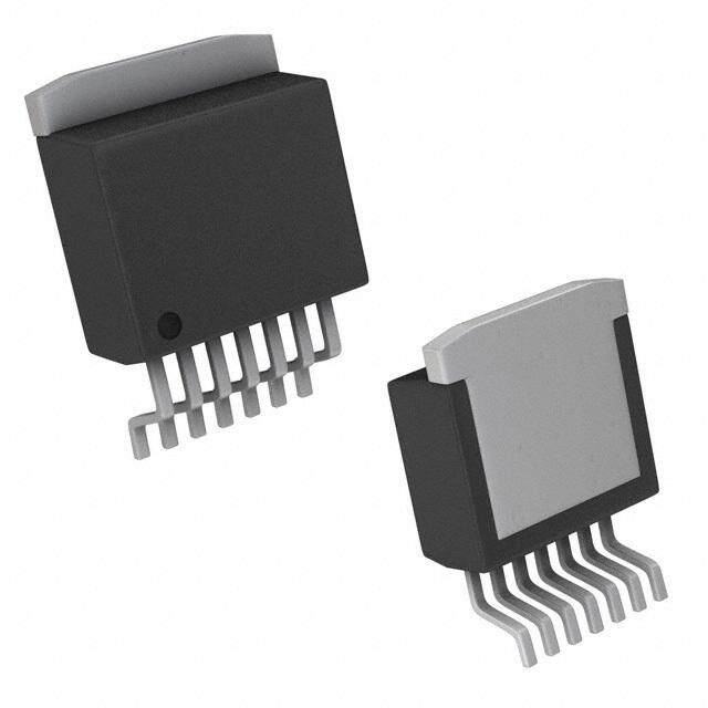
| 产品图片 |
|
| 产品型号 | MP108FD |
| PCN设计/规格 | |
| rohs | 无铅 / 符合限制有害物质指令(RoHS)规范要求 |
| 产品系列 | Apex Precision Power® |
| 产品培训模块 | http://www.digikey.cn/PTM/IndividualPTM.page?site=cn&lang=zhs&ptm=30464 |
| 产品目录页面 | |
| 供应商器件封装 | 34-DIP |
| 其它名称 | 598-1407 |
| 包装 | 管件 |
| 压摆率 | 170 V/µs |
| 增益带宽积 | 10MHz |
| 安装类型 | 通孔 |
| 封装/外壳 | 34-DIP 模块 |
| 工作温度 | -40°C ~ 85°C |
| 放大器类型 | 功率 |
| 标准包装 | 1 |
| 电压-电源,单/双 (±) | 30 V ~ 200 V, ±15 V ~ 100 V |
| 电压-输入失调 | 1mV |
| 电流-电源 | 50mA |
| 电流-输入偏置 | 100pA |
| 电流-输出/通道 | 10A |
| 电路数 | 1 |
| 输出类型 | - |
| 配用 | /product-detail/zh/EK57/598-1470-ND/1762127 |


PDF Datasheet 数据手册内容提取
MP108 • MP108A Power Operational Amplifier FEATURES • Low Cost • High Voltage - 200V • High Output Current - 10A • 100W Dissipation Capability • 300 kHz Power Bandwidth APPLICATIONS • Inkjet Printer Head Drive • Piezo Transducer Drive • Industrial Instrumentation • Reflectometers • Ultra-Sound Transducer Drive DESCRIPTION The MP108 operational amplifier is a surface mount constructed component that provides a cost effec- tive solution in many industrial applications. The MP108 offers outstanding performance that rivals much more expensive hybrid components yet has a footprint of only 4 sq in. The MP108 has many optional features such as four-wire current limit sensing and external compensation. The 300 kHz power bandwidth and 10A output of the MP108 makes it a good choice for piezo transducer drive applications. The MP108 is built on a thermally conductive but electrically insulating substrate that can be mounted to a heat sink. Figure 1: Equivalent Schematic +V 8 B +VB 4 14 +VS GND 3 C1 R1 R2 Q17 R3 15 +VS BPLT 2 Q1A Q1B 16 +VS TP 1 C5 Q2 D1 SBUABCKSTPRLAATTEE Q4 Q7 Q6 R5 Q3 Q8 Q9 11 +OUT D2 12 +OUT C 5 CCC12 6 R15 R7 Q14 13 +OUT R8 Q11 28 +CL Q12 Q13 27 -CL IC1 Q16 20 -OUT -IN 34 R9 Q15A Q15B 21 -OUT R10 R11 Q18 22-OUT +IN 33 R12 Q19 R17 Q22 Q20 GND 32 Q23 Q24 Q21 C3 R19 R20 17 -VS -VB 30 18 -VS -VB 25 19 -VS © Apex Microtechnology Inc. Oct 2016 www.apexanalog.com All rights reserved MP108U Rev H
MP108 • MP108A TYPICAL CONNECTION Figure 2: Typical Connection R F +V +V S B * 0.1μF 0.1μF +V S RI +VB -CL V R OUT +CL CL MP108 OUT C C C R C L -V B * Use 10 μF per Amp -V C S C of output current * 0.1μF 0.1μF -V -V S B 2 MP108U Rev H
MP108 • MP108A EXTERNAL CONNECTIONS Figure 3: Pin-out -IN 34 +IN 33 1 TP GND 32 2 BPLT NC 31 3 GND -VB 30 4 +VB NC 29 5 CC1 MP108 +CL 28 6 CC2 (Viewed from -CL 27 7 NC backplate) NC 26 8 +VB -VB 25 9 NC NC 24 10 NC NC 23 11 +OUT -OUT 22 12 +OUT -OUT 21 13 +OUT -OUT 20 14 +VS -VS 19 15 +VS -VS 18 16 +VS -VS 17 Pin Number Name Description 1 TP Apex test pin, do not connect. 2 BPLT AC coupling to backplate. Connect to signal ground. Ground. Pins 3 and 32 are not connected on the unit. Connect both pins to system 3, 32 GND signal ground. 4, 8 +V The positive boost supply rail. Short to +Vs if unused. See applicable section. B Compensation capacitor connection. Select value based on Phase Compensation. 5, 6 CC See applicable section. The positive current output. Short to -OUT pins. Connect these pins to the MP108 11, 12, 13 +OUT side of the current limit resistor and the +CL pin. Output current is sourced from these pins through the current limit resistor to the load. 14, 15, 16 +Vs The positive supply rail. 17, 18, 19 -Vs The negative supply rail. The negative current output. Short to +OUT pins. Connect these pins to the MP108 20, 21, 22 -OUT side of the current limit resistor and the +CL pin. Output current sinks to these pins through the current limit resistor from the load. 25, 30 -V The negative boost supply rail. Short to -Vs if unused. See applicable section. B Connect to the load side of the current limit resistor and feedback resistor. Current 27 -CL limit will activate as the voltage across R exceeds 0.65 V. CL Connect to the OUT side of the current limit resistor. Current limit will activate as 28 +CL the voltage across R exceeds 0.65 V. CL 33 +IN The non-inverting input. 34 -IN The inverting input. All Others NC No connection. MP108U Rev H 3
MP108 • MP108A SPECIFICATIONS Unless otherwise noted: T = 25°C, C = 100pF. DC input specifications are value given. Power supply voltage C C is typical rating. ±V = ±V . B S ABSOLUTE MAXIMUM RATINGS Parameter Symbol Min Max Units Supply Voltage, total +V to -V 200 V s s Supply Voltage, +VB 1 +VB +VS +15 V Supply Voltage, -VB 1 -VB -VS -15 V Output Current, peak, within SOA I 12 A O Power Dissipation, internal, DC P 100 W D Input Voltage +V to -V V B B Differential Input Voltage ±25 V Temperature, pin solder, 10s 225 °C Temperature, junction 2 TJ 150 °C Temperature, storage -40 +105 °C Operating Temperature Range, case T -40 +85 °C C 1. Power supply voltages +V and -V must not be less than +V-0.6 V and -V +0.6 V respectively. B B s S 2. Long term operation at the maximum junction temperature will result in reduced product life. Derate internal power dis- sipation to achieve high MTTF. 4 MP108U Rev H
MP108 • MP108A INPUT MP108 MP108A Test Parameter Units Conditions Min Typ Max Min Typ Max Offset Voltage 1 5 * 3 mV Offset Voltage vs. Temperature Full temp range 50 * µV/°C Offset Voltage vs. Supply 20 * µV/V Bias Current, initial 1 100 70 pA Bias Current vs. Supply 0.1 * pA/V Offset Current, initial 50 30 pA Input Resistance, DC 1011 * Ω Input Capacitance 4 * pF +V - Common Mode Voltage Range B * V 15 -V + Common Mode Voltage Range B * V 15 Common Mode Rejection, DC 92 * dB 1 MHz BW, R = Noise S 10 * µV RMS 1 kΩ 1. Doubles for every 10°C of case temperature increase GAIN MP108 MP108A Test Parameter Units Conditions Min Typ Max Min Typ Max R = 10 kΩ, C = Open Loop, @ 15 Hz L C 96 * dB 10pF Gain Bandwidth Product @ 1 MHz C = 10pF 10 * MHz C Phase Margin Full temp range 45 * ° C = 10pF, C Power Bandwidth 180V +V = 100V, 300 * kHz P-P S -V = -100V S MP108U Rev H 5
MP108 • MP108A OUTPUT MP108 MP108A Test Parameter Units Conditions Min Typ Max Min Typ Max Voltage Swing I = 10A +V -10 +V -8.6 * * V O S S Voltage Swing I = -10A -V +10 -V +7 * * V O S S I = 10A, +V - Voltage Swing O S * V +V = +V +10V 1.6 B S I = -10A, -V + Voltage Swing O S * V -V = -V -10V 5.1 B S Current, Continuous, DC 10 11 A Slew Rate, A = -20 C = 10pF 150 170 * * V/µs V C Settling Time to 0.1% 2V step 1 * µs Resistance No load, DC 5 * Ω POWER SUPPLY MP108 MP108A Test Parameter Units Conditions Min Typ Max Min Typ Max Voltage ±15 ±75 ±100 * * * V Current, quiescent 50 65 * * mA THERMAL MP108 MP108A Test Parameter Units Conditions Min Typ Max Min Typ Max Full temp range, Resistance, AC, junction to case 1 1 * °C/W F ≥ 60 Hz Full temp range, Resistance, DC, junction to case 1.25 * °C/W F < 60 Hz Resistance, junction to air Full temp range 13 * °C/W Temperature Range, case -40 +85 * * °C 1. Rating applies if the output current alternates between both output transistors at a rate faster than 60 Hz. Note: *The specification of MP108A is identical to the specification for MP108 in the applicable column to the left. 6 MP108U Rev H
MP108 • MP108A TYPICAL PERFORMANCE GRAPHS Figure 4: Power Derating Figure 5: Phase Response W/ Boost 100 90 3 ) (cid:116) 2 (cid:894) (cid:87)(cid:3) 80 (cid:374)(cid:853)(cid:3) 120 1 (cid:381) (cid:415) (cid:393)(cid:258) 60 (cid:931)(cid:895) (cid:400)(cid:400)(cid:349) (cid:711)(cid:3)(cid:894) 2 (cid:24)(cid:349) e, 150 (cid:396)(cid:3) s (cid:286) 40 a (cid:449) h (cid:381) P 1 C = 10pF (cid:87) 2 CC = 33pF 1 (cid:258)(cid:367)(cid:3) 180 C (cid:374) 20 3 C = 100pF (cid:396) C (cid:286) R(cid:3)(cid:1089)(cid:3)(cid:1008)(cid:3)(cid:591) (cid:374)(cid:410) L (cid:47) I = 1A O 0 210 -40 -20 0 20 40 60 80 100 100k 1M 5M Case Temperature, T (°C) Frequency, F (Hz) C Figure 6: Phase Response W/O Boost Figure 7: Small Signal Response W/ Boost 90 120 2 3 100 1 ) CC = 33pF B d (cid:711)(cid:3)(cid:894)(cid:931)(cid:895) 120 ain, A ( 80 CC = C22 =0 p4F70pF se, 2 p G 60 C a o h o P 150 1 CC = 10pF n L 40 2 C = 33pF e C p 3 C = 100pF 1 O R(cid:3)(cid:1089)(cid:3)(cid:1008)(cid:3)(cid:591) R(cid:3)(cid:1089)C(cid:3)(cid:1008)(cid:3)(cid:591) 20 IL = 1A L O I = 1A O 180 0 300k 1M 10M 1 10 100 1k 10k 100k 1M 10M Frequency, F (Hz) Frequency, F (Hz) MP108U Rev H 7
MP108 • MP108A Figure 8: Small Signal Response Figure 9: Power Response W/O Boost 120 200 C = 10pF C C Gain, A (dB) 1086000 CC = 33pCFC = 100pF ge, V(V)o P-P 100 CC = 33pFC = 10pF a Open Loop 4200 R(cid:3)(cid:1089)(cid:3)(cid:1008)(cid:3)(cid:591) Output Volt CC = 470pF CC = 220pF CC = 100p L F I = 1A DC O 0 0 1 10 100 1k 10k 100k 1M 10k 100k 1M 5M Frequency, F (Hz) Frequency, F (Hz) Figure 10: Current Limit Figure 11: Quiescent Current vs. Supply 130 120 ) % ( t (%) 120 ent, Io 100 mi r nt Li 110 t Cur TC = 85°C e n rr 100 ce 80 u s C e alized 90 ed Qui 60 TC = 25°C TC = -40°C m z r ali o 80 m N r o N 40 70 0 40 80 120 160 200 -50 -25 0 25 50 75 100 Total Supply Voltage, V (V) Case Temperature, T (°C) S C 8 MP108U Rev H
MP108 • MP108A Figure 12: Quiescent Current vs. Figure 13: Harmonic Distortion Temperature 115 1 %) A = 20 ( V Q C = 10pF t, I 110 VC = 52V n S rre ) (cid:1081) 0.1 RL(cid:3)(cid:1089)(cid:3)(cid:1008)(cid:3)(cid:591) 0W nt Cu 105 (cid:44)(cid:24)(cid:3)(cid:894) P O= 20 W esce (cid:381)(cid:374)(cid:853)(cid:3)(cid:100) = 100 ui 100 (cid:415) P O d Q (cid:400)(cid:410)(cid:381)(cid:396) 0.01 P = 10W e (cid:24)(cid:349) O z ali 95 m r o N 90 0.001 -40 -20 0 20 40 60 80 100 30 100 1k 10k 30k Case Temperature (°C) Frequency, F (Hz) Figure 14: Output Voltage Swing 9 ) 8 W/O BOOST FROM +VS V y ( 7 pl m Sup 65 W/O BOOST FROM -V S o r p F 4 Voltage Dro 132 T5C0 m= 2s 5P°UCLSE WWIITTHH BB OO OO SSTT FFRROOMM - V+VS S 0 0 2 4 6 8 10 Output Current, I (A) o MP108U Rev H 9
MP108 • MP108A SAFE OPERATING AREA (SOA) The MOSFET output stage of the MP108 is not limited by second breakdown considerations as in bipolar output stages. Only thermal considerations and current handling capabilities limit the SOA. The output stage is protected against transient flyback by the parasitic body diodes of the output stage MOSFET structure. However, for protection against sustained high energy flyback external fast reverse recovery diodes must be used. Figure 15: SOA 20 ) A ( S 10 V (cid:882) (cid:1005) (cid:3) (cid:1004) (cid:396) (cid:381) (cid:1005) (cid:373) (cid:400) VS (cid:1004)(cid:1004) (cid:853)(cid:3)(cid:100) (cid:373)(cid:3)(cid:1085) (cid:24)(cid:18)(cid:853)(cid:3) (cid:373)(cid:400)(cid:853)(cid:3)(cid:100) C=25° (cid:381) (cid:24) (cid:100) C=2 C (cid:396) (cid:18)(cid:853)(cid:3) C=2 5° (cid:38) (cid:100) 5 C (cid:410)(cid:3) C= °C (cid:374) 8 5 (cid:286) ° C (cid:396) 1 (cid:396) (cid:437) (cid:18) (cid:3) (cid:410) (cid:437) (cid:393) (cid:410) (cid:437) (cid:75) 0.2 1 10 100 200 (cid:94)(cid:437)(cid:393)(cid:393)(cid:367)(cid:455)(cid:3)(cid:410)(cid:381)(cid:3)(cid:75)(cid:437)(cid:410)(cid:393)(cid:437)(cid:410)(cid:3)(cid:24)(cid:349)(cid:299)(cid:286)(cid:396)(cid:286)(cid:374)(cid:415)(cid:258)(cid:367)(cid:853)(cid:3)V - V (V) S o 10 MP108U Rev H
MP108 • MP108A GENERAL Please read Application Note 1 “General Operating Considerations” which covers stability, supplies, heat sinking, mounting, current limit, SOA interpretation, and specification interpretation. Visit www.apexana- log.com for Apex Microtechnology’s complete Application Notes library, Technical Seminar Workbook, and Evaluation Kits. TYPICAL APPLICATION INKJET NOZZLE DRIVE MP108's fast slew rate and wide power bandwidth make it an ideal nozzle driver for industrial inkjet printers. The 10A output capability can drive hundreds of nozzles simultaneously. Figure 16: Typical Application GROUND PINS The MP108 has two ground pins (pins 3, 32). These pins provide a return for the internal capacitive bypassing of the small signal portions of the MP108. The two ground pins are not connected together on the substrate. Both of these pins are required to be connected to the system signal ground. PHASE COMPENSATION The external compensation capacitor C is connected between pins 5 and 6. Unity gain stability can C be achieved with any capacitor value larger than 100 pF for a minimum phase margin of 45 degrees. At higher gains more phase shift can usually be tolerated in most designs and the compensation capacitor value can be reduced resulting in higher bandwidth and slew rate. Use the typical operating curves and the table in this MP108U Rev H 11
MP108 • MP108A section as a guide to select C for the application. An NPO (COG) type capacitor is required rated for the full C supply voltage (200 V). Gain w/o C Typ. Slew Rate C boost 1 100 pF 55 V/µs 4 33 pF 135 V/µs 10 10 pF 170 V/µs Gain with C Typ. Slew Rate C boost 1 471 pF 12 V/µs 3 220 pF 35 V/µs 10 33 pF 135 V/µs OVERVOLTAGE PROTECTION Although the MP108 can withstand differential input voltages up to ±25V, additional external protection is recommended. In most applications 1N4148 signal diodes connected anti-parallel across the input pins is sufficient. In more demanding applications where bias current is important diode connected JFETs such as 2N4416 will be required. See Q1 and Q2 in Figure 17. In either case the differential input voltage will be clamped to ±0.7V. This is usually sufficient overdrive to produce the maximum power bandwidth. Some appli- cations will also need over voltage protection devices connected to the power supply rails. Unidirectional transient voltage suppressor diodes or zener diodes are recommended. These diodes clamp transients to voltages within the power supply rating and also clamp power supply reversals to ground. Whether TVS or zener diodes are used or not the system power supply should be evaluated for transient performance includ- ing power-on overshoot and power-off polarity reversals as well as line regulation. See Z1 and Z2 in Figure 17. Figure 17: Overvoltage Protection 12 MP108U Rev H
MP108 • MP108A POWER SUPPLY BYPASSING Bypass capacitors to power supply terminals +V and -V must be connected physically close to the pins S S to prevent local parasitic oscillation in the output stage of the MP108. Use electrolytic capacitors at least 10µF per output amp required. Bypass the electrolytic capacitors with high quality ceramic capacitors (X7R) 0.1µF or greater. In most applications power supply terminals +V and -V will be connected to +V and -V B B S S respectively. Supply voltages +V and -V are bypassed internally but both ground pins 3 and 32 must be con- B B nected to the system signal ground to be effective. In all cases power to the buffer amplifier stage of the MP108 at pins 8 and 25 must be connected to +V and -V at pins 4 and 30 respectively. Provide local bypass B B capacitors at pins 8 and 25. See figure 2 for Typical Connection Diagram. CURRENT LIMIT The two current limit sense lines are to be connected directly across the current limit sense resistor. For the current limit to work correctly pin 28 must be connected to the amplifier output side and pin 27 con- nected to the load side of the current limit resistor R as shown in Figure 18. This connection will bypass LIM any parasitic resistances R , formed by socket and solder joints as well as internal amplifier losses. The cur- P rent limiting resistor may not be placed anywhere in the output circuit except where shown in Figure 18. The value of the current limit resistor can be calculated as follows: 0.65V R = ------------------------ CL I A LIMIT Figure 18: 4-Wire Current Limit BOOST OPERATION With the boost feature the small signal stages of the amplifier are operated at higher supply voltages than the amplifier’s high current output stage. +V (pins 4,8) and -V (pins 25,30) are connected to the small B B signal stages and +V (pins 14-16) and -V (pins 17-19) are connected to the high current output stage. An S S additional 10V on the +V and -V pins is sufficient to allow the small signal stages to drive the output stage B B MP108U Rev H 13
MP108 • MP108A into the triode region and improve the output voltage swing for extra efficient operation when required. When the boost feature is not needed +V and -V are connected to the +V and -V pins respectively. The S S B B +V and -V pins must not be operated at supply voltages less than +V -0.6 V and -V +0.6 V respectively. B B S S BACKPLATE GROUNDING The substrate of the MP108 is an insulated metal substrate. It is required that it be connected to signal ground. Connect pin 2 (back plate) to signal ground. The back plate will then be AC grounded to signal ground through a 1µF capacitor. 14 MP108U Rev H
MP108 • MP108A PACKAGE OPTIONS Part Number Apex Package Style Description MP108 FD 34-pin Open Frame MP108A FD 34-pin Open Frame PACKAGE STYLE FD 2.200 [55.88] 1.100 (cid:287).129 C.O26M [P6O.6N]ENT PIN 1 [27.94.]450 4 [P(cid:287)L3A.2C8E]S CLEARANCE [11.43] 1.63+.02 1 [1.66.5501] [41.4+--.000..25511] [1.677.002] CL CL 1.300 [33.02] 1.340 [34.04] .150 [3.81] CL NOTES: .380 2.49+-..00 22[63.2+-00..5511] 1. Dimensions are inches; alternate units are [mm]. [9.65] 2. Recommended PCB hole diameter for pins: .050 [1.27]. .070 3. 2oz. copper over 600V dielectric over aluminum substrate. [1.78] .025 .100 4. Tin over nickel plated phosphor bronze pins. [0.63] [2.54] 5. Package weight: 18g or .63oz. SQ. PIN TYP. 6. Mount with #4 [M3] or equivalent screws. 7. It is not recommended that mounting of the package rely on the pins for mechanical support. NEED TECHNICAL HELP? CONTACT APEX SUPPORT! For all Apex Microtechnology product questions and inquiries, call toll free 800-546-2739 in North America. For inquiries via email, please contact apex.support@apexanalog.com. International customers can also request support by contacting their local Apex Microtechnology Sales Representative. To find the one nearest to you, go to www.apexanalog.com IMPORTANT NOTICE Apex Microtechnology, Inc. has made every effort to insure the accuracy of the content contained in this document. However, the information is subject to change without notice and is provided "AS IS" without warranty of any kind (expressed or implied). Apex Microtechnology reserves the right to make changes without further notice to any specifications or products mentioned herein to improve reliability. This document is the property of Apex Microtechnology and by furnishing this information, Apex Microtechnology grants no license, expressed or implied under any patents, mask work rights, copyrights, trademarks, trade secrets or other intellectual property rights. Apex Microtechnology owns the copyrights associated with the information contained herein and gives consent for copies to be made of the information only for use within your organization with respect to Apex Microtechnology integrated circuits or other products of Apex Microtechnology. This consent does not extend to other copying such as copying for general distribution, advertising or promotional purposes, or for creating any work for resale. APEX MICROTECHNOLOGY PRODUCTS ARE NOT DESIGNED, AUTHORIZED OR WARRANTED TO BE SUITABLE FOR USE IN PRODUCTS USED FOR LIFE SUPPORT, AUTOMOTIVE SAFETY, SECURITY DEVICES, OR OTHER CRITICAL APPLICATIONS. PRODUCTS IN SUCH APPLICATIONS ARE UNDERSTOOD TO BE FULLY AT THE CUSTOMER OR THE CUSTOMER’S RISK. Apex Microtechnology, Apex and Apex Precision Power are trademarks of Apex Microtechnology, Inc. All other corporate names noted herein may be trademarks of their respective holders. MP108U Rev H 15