 Datasheet下载
- 型号: TS339IPT
- 制造商: STMicroelectronics
- 库位|库存: xxxx|xxxx
- 要求:
| 数量阶梯 | 香港交货 | 国内含税 |
| +xxxx | $xxxx | ¥xxxx |
查看当月历史价格
查看今年历史价格
TS339IPT产品简介:
ICGOO电子元器件商城为您提供TS339IPT由STMicroelectronics设计生产,在icgoo商城现货销售,并且可以通过原厂、代理商等渠道进行代购。 TS339IPT价格参考。STMicroelectronicsTS339IPT封装/规格:线性 - 比较器, 通用 比较器 CMOS,开路漏极 14-TSSOP。您可以下载TS339IPT参考资料、Datasheet数据手册功能说明书,资料中有TS339IPT 详细功能的应用电路图电压和使用方法及教程。
STMicroelectronics的TS339IPT是一款四路电压比较器,属于线性比较器类别。它广泛应用于需要将模拟信号与参考电平进行比较的场合,常用于电平检测、窗口检测、电压监控和控制系统中。

该器件采用低功耗设计,适用于电池供电设备和便携式电子产品,如笔记本电脑、智能仪表和工业控制系统。TS339IPT可在宽温度范围内稳定工作,因此也适合工业级应用,例如传感器信号处理、过压/欠压保护电路和阈值检测系统。

此外,该比较器支持单电源供电,简化了电源设计,提高了系统的可靠性和灵活性。其高精度和稳定性使其在自动化控制、电机驱动保护和电源管理模块中也有广泛应用。
| 参数 | 数值 |
| 产品目录 | 集成电路 (IC)半导体 |
| CMRR,PSRR(典型值) | 75dB CMRR |
| 描述 | IC COMP MICROPWR QUAD V 14 TSSOP模拟比较器 Micropower Quad Volt |
| 产品分类 | |
| 品牌 | STMicroelectronics |
| 产品手册 | |
| 产品图片 |
|
| rohs | 符合RoHS无铅 / 符合限制有害物质指令(RoHS)规范要求 |
| 产品系列 | 校验器 IC,STMicroelectronics TS339IPT- |
| 数据手册 | |
| 产品型号 | TS339IPT |
| 产品目录页面 | |
| 产品种类 | 模拟比较器 |
| 传播延迟(最大值) | - |
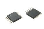
| 供应商器件封装 | 14-TSSOP |
| 偏转电压—最大值 | 5 mV |
| 元件数 | 4 |
| 其它名称 | 497-2266-1 |
| 其它有关文件 | http://www.st.com/web/catalog/sense_power/FM123/SC60/SS1/PF65395?referrer=70071840 |
| 包装 | 剪切带 (CT) |
| 响应时间 | 1.5 us |
| 商标 | STMicroelectronics |
| 安装类型 | 表面贴装 |
| 安装风格 | SMD/SMT |
| 封装 | Reel |
| 封装/外壳 | 14-TSSOP(0.173",4.40mm 宽) |
| 封装/箱体 | TSSOP-14 |
| 工作温度 | -40°C ~ 125°C |
| 工厂包装数量 | 2500 |
| 最大功率耗散 | 710 mW |
| 最大工作温度 | + 125 C |
| 最小工作温度 | - 40 C |
| 标准包装 | 1 |
| 滞后 | - |
| 电压-电源,单/双 (±) | 2.7 V ~ 16 V, ±1.35 V ~ 8 V |
| 电压-输入失调(最大值) | 5mV @ 10V |
| 电流-输入偏置(最大值) | 1pA @ 5V |
| 电流-输出(典型值) | 20mA |
| 电流-静态(最大值) | 25µA |
| 电源电压-最大 | 16 V |
| 电源电压-最小 | 2.7 V |
| 电源电流 | 20 uA |
| 电源电流—最大值 | 20 uA |
| 类型 | 通用 |
| 系列 | TS339 |
| 输入偏压电流—最大 | 600 pA |
| 输出电流—典型值 | 2 nA |
| 输出类型 | CMOS,开路漏极 |
| 通道数量 | 4 Channel |


- 商务部:美国ITC正式对集成电路等产品启动337调查
- 曝三星4nm工艺存在良率问题 高通将骁龙8 Gen1或转产台积电
- 太阳诱电将投资9.5亿元在常州建新厂生产MLCC 预计2023年完工
- 英特尔发布欧洲新工厂建设计划 深化IDM 2.0 战略
- 台积电先进制程称霸业界 有大客户加持明年业绩稳了
- 达到5530亿美元!SIA预计今年全球半导体销售额将创下新高
- 英特尔拟将自动驾驶子公司Mobileye上市 估值或超500亿美元
- 三星加码芯片和SET,合并消费电子和移动部门,撤换高东真等 CEO
- 三星电子宣布重大人事变动 还合并消费电子和移动部门
- 海关总署:前11个月进口集成电路产品价值2.52万亿元 增长14.8%


PDF Datasheet 数据手册内容提取
TS339 Micropower quad CMOS voltage comparator Datasheet - production data Features • Extremely low supply current: 9 μA typ./comparator D • Wide single supply range 2.7 V to 16 V or dual SO14 supplies (±1.35 V to ±8 V) (plastic micropackage) • Extremely low input bias current: 1 pA typ. • Extremely low input offset current: 1 pA typ. • Input common-mode voltage range includes GND P • High input impedance: 1012 Ω typ. TSSOP14 (thin shrink small outline package) • Fast response time: 1.5 μs typ. for 5 mV overdrive • Pin-to-pin and functionally compatible with bipolar LM339 device (cid:50)(cid:88)(cid:87)(cid:83)(cid:88)(cid:87)(cid:3)(cid:21) (cid:20) (cid:20)(cid:23) (cid:50)(cid:88)(cid:87)(cid:83)(cid:88)(cid:87)(cid:3)(cid:22) (cid:50)(cid:88)(cid:87)(cid:83)(cid:88)(cid:87)(cid:3)(cid:20) (cid:21) (cid:20)(cid:22) (cid:50)(cid:88)(cid:87)(cid:83)(cid:88)(cid:87)(cid:3)(cid:23) Description (cid:57)(cid:38)(cid:38)(cid:14) (cid:22) (cid:20)(cid:21) (cid:57)(cid:38)(cid:38)(cid:16) (cid:44)(cid:81)(cid:89)(cid:72)(cid:85)(cid:87)(cid:76)(cid:81)(cid:74)(cid:3)(cid:76)(cid:81)(cid:83)(cid:88)(cid:87)(cid:3)(cid:20) (cid:23) (cid:16) (cid:14) (cid:20)(cid:20) (cid:49)(cid:82)(cid:81)(cid:16)(cid:76)(cid:81)(cid:89)(cid:72)(cid:85)(cid:87)(cid:76)(cid:81)(cid:74)(cid:3)(cid:76)(cid:81)(cid:83)(cid:88)(cid:87)(cid:3)(cid:23) The TS339 device is a micro-power, CMOS, quad (cid:49)(cid:82)(cid:81)(cid:16)(cid:76)(cid:81)(cid:89)(cid:72)(cid:85)(cid:87)(cid:76)(cid:81)(cid:74)(cid:3)(cid:76)(cid:81)(cid:83)(cid:88)(cid:87)(cid:3)(cid:20) (cid:24) (cid:14) (cid:16) (cid:20)(cid:19) (cid:44)(cid:81)(cid:89)(cid:72)(cid:85)(cid:87)(cid:76)(cid:81)(cid:74)(cid:3)(cid:76)(cid:81)(cid:83)(cid:88)(cid:87)(cid:3)(cid:23) voltage comparator with extremely low (cid:44)(cid:81)(cid:89)(cid:72)(cid:85)(cid:87)(cid:76)(cid:81)(cid:74)(cid:3)(cid:76)(cid:81)(cid:83)(cid:88)(cid:87)(cid:3)(cid:21) (cid:25) (cid:16) (cid:14) (cid:28) (cid:49)(cid:82)(cid:81)(cid:16)(cid:76)(cid:81)(cid:89)(cid:72)(cid:85)(cid:87)(cid:76)(cid:81)(cid:74)(cid:3)(cid:76)(cid:81)(cid:83)(cid:88)(cid:87)(cid:3)(cid:22) consumption of 9 μA typ./comparator (20 times (cid:49)(cid:82)(cid:81)(cid:16)(cid:76)(cid:81)(cid:89)(cid:72)(cid:85)(cid:87)(cid:76)(cid:81)(cid:74)(cid:3)(cid:76)(cid:81)(cid:83)(cid:88)(cid:87)(cid:3)(cid:21) (cid:26) (cid:14) (cid:16) (cid:27) (cid:44)(cid:81)(cid:89)(cid:72)(cid:85)(cid:87)(cid:76)(cid:81)(cid:74)(cid:3)(cid:76)(cid:81)(cid:83)(cid:88)(cid:87)(cid:3)(cid:22) less than the bipolar LM339). Similar performances are offered by the quad micro- Pin connections power comparator TS3704 with a push-pull top view CMOS output. Thus response times remain similar to the LM339 device. Table 1. Device s ummary Order code Temperature range Package Packaging Marking TS339CD/CDT 0 °C, 70 °C S339C SO14 Tube or tape and reel TS339IDT -40 °C, 125 °C S339I TS339IPT TSSOP14 Tape and reel February 2014 DocID4065 Rev 4 1/11 This is information on a product in full production. www.st.com
Contents TS339 Contents 1 Absolute maximum ratings . . . . . . . . . . . . . . . . . . . . . . . . . . . . . . . . . . . 3 2 Typical application schematics . . . . . . . . . . . . . . . . . . . . . . . . . . . . . . . . 4 3 Electrical characteristics . . . . . . . . . . . . . . . . . . . . . . . . . . . . . . . . . . . . . 5 4 Package information . . . . . . . . . . . . . . . . . . . . . . . . . . . . . . . . . . . . . . . . . 7 4.1 SO14 package . . . . . . . . . . . . . . . . . . . . . . . . . . . . . . . . . . . . . . . . . . . . . . 8 4.2 TSSOP14 package . . . . . . . . . . . . . . . . . . . . . . . . . . . . . . . . . . . . . . . . . . . 9 5 Revision history . . . . . . . . . . . . . . . . . . . . . . . . . . . . . . . . . . . . . . . . . . . 10 2/11 DocID4065 Rev 4
TS339 Absolute maximum ratings 1 Absolute maximum ratings Table 2. Key parameters and their absolute maximum ratings Symbol Parameter Value Unit V + Supply voltage(1) 18 CC V Differential input voltage(2) ±18 id V V Input voltage(3) 18 i V Output voltage 18 o I Output current 20 o mA I Forward current in ESD protection diodes on inputs(4) 50 F Power dissipation(5) pd SO14 830 mW TSSOP14 710 T Storage temperature range -65 to +150 °C stg HBM: human body model(6) 50 ESD MM: machine model(7) 40 V CDM: charged device model 800 1. All voltage values, except the differential voltage, are with respect to network ground terminal. 2. Differential voltages are the non-inverting input terminal with respect to the inverting input terminal. 3. Excursions of input voltages may exceed the power supply level. As long as the common mode voltage [V =(V + + V -)/2] remains within the specified range, the comparator will provide a stable output state. icm in in However, the maximum current through the ESD diodes (IF) of the input stage must strictly be observed. 4. Guaranteed by design. 5. Pd is calculated with T = +25 °C, T = +150 °C and amb j R = 150 °C/W for SO14 package thja R = 175 °C/W for TSSOP14 package. thja 6. Human body model, 100pF discharged through a 1.5 kΩ resistor into pin of device. 7. Machine model ESD, a 200 pF cap is charged to the specified voltage, then discharged directly into the IC with no external series resistor (internal resistor < 5 Ω), into pin to pin of device. DocID4065 Rev 4 3/11 11
Typical application schematics TS339 2 Typical application schematics Figure 1. Schematic diagram (for 1/4 TS339) VCC+ T10 T1 T2 T9 T17 R1 T11 T12 T18 Input- Input+ T3 T 4 Output T20 T13 T8 T19 T5 T7 T14 T15 T16 T6 VCC- 4/11 DocID4065 Rev 4
TS339 Electrical characteristics 3 Electrical characteristics T able 3. V + = 3 V, V - = 0 V, T = 25 °C (unless otherwise specified) CC CC amb Symbol Parameter Min. Typ. Max. Unit Input offset voltage(1) V V = 1.5 V 5 mV io ic T . ≤ T ≤ T 6.5 min amb max. Input offset current(2) I V = 1.5 V 1 io ic T . ≤ T ≤ T 300 min amb max. pA Input bias current (2) I V = 1.5 V 1 ib ic T . ≤ T ≤ T 600 min amb max. Input common mode voltage range 0 V +-1.2 V CC V icm T . ≤ T ≤ T 0 V + -1.5 min amb max CC Common-mode rejection ratio CMR V = V 70 ic icm min. dB Supply voltage rejection ratio SVR V + = 3 V to 5 V 70 CC High level output current I V = +1 V, V = 3 V 2 40 nA OH id OH T . ≤ T ≤ T 1000 min amb max. Low level output voltage V V = -1 V, I = +6 mA 400 550 mV OL id OL T . ≤ T ≤ T 800 min amb max. Supply current (each comparator) I No load - outputs low 9 20 μA CC T . ≤ T ≤ T 25 min amb max. Response time low to high t V = 0 V, f = 10 kHz, T . ≤ T ≤ T C = 50 pF, overdrive = 5 mV 1.5 PLH ic min amb max L TTL input 0.7 μs Response time high to low t V = 0 V, f = 10 kHz, R = 5.1 kΩ, C = 50 pF, overdrive = 5 mV 2.5 PHL ic L L TTL input 0.08 1. The specified offset voltage is the maximum value required to drive the output up to 2.5 V or down to 0.3 V. 2. Maximum values including unavoidable inaccuracies of the industrial test. DocID4065 Rev 4 5/11 11
Electrical characteristics TS339 T able 4. V + = 5 V, V - = 0 V, T = 25 °C (unless otherwise specified) CC CC amb Symbol Parameter Min. Typ. Max. Unit Input offset voltage(1) V V = 2.5 V, V + = 5 V to 10 V 1.4 5 mV io ic cc T . ≤ T ≤ T 6.5 min amb max. Input offset current(2) I V = 2.5 V 1 io ic T . ≤ T ≤ T 300 min amb max. pA Input bias current(2) I V = 2.5 V 1 ib ic T . ≤ T ≤ T 600 min amb max. Input common mode voltage range 0 V +-1.2 V CC V icm T . ≤ T ≤ T 0 V + -1.5 min amb max CC Common-mode rejection ratio CMR V = 0 V 75 ic dB Supply voltage rejection ratio SVR V + = +5 V to +10 V 85 CC High level output voltage I V = 1 V, V = +5 V 27 40 nA OH id OH T . ≤ T ≤ T 1000 min amb max. Low level output voltage V V = -1 V, I = 6 mA 260 400 mV OL id OL T . ≤ T ≤ T 650 min amb max. Supply current (each comparator) 10 20 I No load - outputs low μA CC 25 T . ≤ T ≤ T min amb max. Response time low to high V = 0 V, f = 10 kHz, R = 5.1 kΩ, C = 15 pF, overdrive = 5 mV 1.5 ic L L Overdrive = 10 mV 1.2 t PLH Overdrive = 20 mV 1.1 Overdrive = 40 mV 0.9 TTL input 0.8 μs Response time high to low V = 0 V, f = 10 kHz, R = 5.1 kΩ, C = 15 pF, overdrive = 5 mV 2.5 ic L L Overdrive = 10 mV 1.9 t PHL Overdrive = 20 mV 1.2 Overdrive = 40 mV 0.8 TTL input 0.08 Fall time t ns f f = 10 kHz, C = 50 pF, R = 5.1 kΩ, overdrive 50 mV 30 L L 1. The specified offset voltage is the maximum value required to drive the output up to 4.5 V or down to 0.3 V. 2. Maximum values including unavoidable inaccuracies of the industrial test. 6/11 DocID4065 Rev 4
TS339 Package information 4 Package information In order to meet environmental requirements, ST offers these devices in different grades of ECOPACK® packages, depending on their level of environmental compliance. ECOPACK specifications, grade definitions and product status are available at: www.st.com. ECOPACK is an ST trademark. DocID4065 Rev 4 7/11 11
Package information TS339 4.1 SO14 package information Figure 2. SO14 package outline Table 5. SO14 package mechanical data Dimensions Symbol mm inch Min. Typ. Max. Min. Typ. Max. A 1.75 0.068 a1 0.1 0.2 0.003 0.007 a2 1.65 0.064 b 0.35 0.46 0.013 0.018 b1 0.19 0.25 0.007 0.010 C 0.5 0.019 c1 45° (typ.) D 8.55 8.75 0.336 0.344 E 5.8 6.2 0.228 0.244 e 1.27 0.050 e3 7.62 0.300 F 3.8 4.0 0.149 0.157 G 4.6 5.3 0.181 0.208 L 0.5 1.27 0.019 0.050 M 0.68 0.026 S 8° (max.) 8/11 DocID4065 Rev 4
TS339 Package information 4.2 TSSOP14 package information Figure 3. TSSOP14 package outline (cid:36) (cid:36)(cid:21) (cid:46) (cid:47) (cid:36)(cid:20) (cid:69) (cid:72) (cid:70) (cid:40) (cid:39) (cid:40)(cid:20) (cid:51)(cid:44)(cid:49)(cid:3)(cid:20)(cid:3)(cid:44)(cid:39)(cid:40)(cid:49)(cid:55)(cid:44)(cid:41)(cid:44)(cid:38)(cid:36)(cid:55)(cid:44)(cid:50)(cid:49) (cid:20) (cid:19)(cid:19)(cid:27)(cid:19)(cid:22)(cid:22)(cid:26)(cid:39) Table 6. TSSOP14 package mechanical data Dimensions Symbol mm. inch Min. Typ. Max. Min. Typ. Max. A 1.2 0.047 A1 0.05 0.15 0.002 0.004 0.006 A2 0.8 1 1.05 0.031 0.039 0.041 b 0.19 0.30 0.007 0.012 c 0.09 0.20 0.004 0.0089 D 4.9 5 5.1 0.193 0.197 0.201 E 6.2 6.4 6.6 0.244 0.252 0.260 E1 4.3 4.4 4.48 0.169 0.173 0.176 e 0.65 BSC 0.0256 BSC K 0° 8° 0° 8° L 0.45 0.60 0.75 0.018 0.024 0.030 DocID4065 Rev 4 9/11 11
Revision history TS339 5 Revision history Table 7. Document revision history Date Revision Changes Jan. 2003 1 Initial release. 1 - PPAP references inserted in the datasheet see Table 1: Order codes on page 1. Aug. 2005 2 2 - ESD protection inserted in Table 2 Key parameters and their absolute maximum ratings on page 2. Updated Features, Table 1, removed TS339IYD and TS339IYDT from Table 1. 04-Sep-2012 3 Updated ECOPACK text, reformatted Section 4: Package information. Minor corrections throughout document. Removed DIP package Features: updated fast response time 21-Feb-2014 4 Device summary: removed order codes TS339CN, TS339IN, and TS339ID; added temperature range for order codes TS339IDT and TS339IPT 10/11 DocID4065 Rev 4
TS339 Please Read Carefully: Information in this document is provided solely in connection with ST products. STMicroelectronics NV and its subsidiaries (“ST”) reserve the right to make changes, corrections, modifications or improvements, to this document, and the products and services described herein at any time, without notice. All ST products are sold pursuant to ST’s terms and conditions of sale. Purchasers are solely responsible for the choice, selection and use of the ST products and services described herein, and ST assumes no liability whatsoever relating to the choice, selection or use of the ST products and services described herein. No license, express or implied, by estoppel or otherwise, to any intellectual property rights is granted under this document. If any part of this document refers to any third party products or services it shall not be deemed a license grant by ST for the use of such third party products or services, or any intellectual property contained therein or considered as a warranty covering the use in any manner whatsoever of such third party products or services or any intellectual property contained therein. UNLESS OTHERWISE SET FORTH IN ST’S TERMS AND CONDITIONS OF SALE ST DISCLAIMS ANY EXPRESS OR IMPLIED WARRANTY WITH RESPECT TO THE USE AND/OR SALE OF ST PRODUCTS INCLUDING WITHOUT LIMITATION IMPLIED WARRANTIES OF MERCHANTABILITY, FITNESS FOR A PARTICULAR PURPOSE (AND THEIR EQUIVALENTS UNDER THE LAWS OF ANY JURISDICTION), OR INFRINGEMENT OF ANY PATENT, COPYRIGHT OR OTHER INTELLECTUAL PROPERTY RIGHT. ST PRODUCTS ARE NOT DESIGNED OR AUTHORIZED FOR USE IN: (A) SAFETY CRITICAL APPLICATIONS SUCH AS LIFE SUPPORTING, ACTIVE IMPLANTED DEVICES OR SYSTEMS WITH PRODUCT FUNCTIONAL SAFETY REQUIREMENTS; (B) AERONAUTIC APPLICATIONS; (C) AUTOMOTIVE APPLICATIONS OR ENVIRONMENTS, AND/OR (D) AEROSPACE APPLICATIONS OR ENVIRONMENTS. WHERE ST PRODUCTS ARE NOT DESIGNED FOR SUCH USE, THE PURCHASER SHALL USE PRODUCTS AT PURCHASER’S SOLE RISK, EVEN IF ST HAS BEEN INFORMED IN WRITING OF SUCH USAGE, UNLESS A PRODUCT IS EXPRESSLY DESIGNATED BY ST AS BEING INTENDED FOR “AUTOMOTIVE, AUTOMOTIVE SAFETY OR MEDICAL” INDUSTRY DOMAINS ACCORDING TO ST PRODUCT DESIGN SPECIFICATIONS. PRODUCTS FORMALLY ESCC, QML OR JAN QUALIFIED ARE DEEMED SUITABLE FOR USE IN AEROSPACE BY THE CORRESPONDING GOVERNMENTAL AGENCY. Resale of ST products with provisions different from the statements and/or technical features set forth in this document shall immediately void any warranty granted by ST for the ST product or service described herein and shall not create or extend in any manner whatsoever, any liability of ST. ST and the ST logo are trademarks or registered trademarks of ST in various countries. Information in this document supersedes and replaces all information previously supplied. The ST logo is a registered trademark of STMicroelectronics. All other names are the property of their respective owners. © 2014 STMicroelectronics - All rights reserved STMicroelectronics group of companies Australia - Belgium - Brazil - Canada - China - Czech Republic - Finland - France - Germany - Hong Kong - India - Israel - Italy - Japan - Malaysia - Malta - Morocco - Philippines - Singapore - Spain - Sweden - Switzerland - United Kingdom - United States of America www.st.com DocID4065 Rev 4 11/11 11
Mouser Electronics Authorized Distributor Click to View Pricing, Inventory, Delivery & Lifecycle Information: S TMicroelectronics: TS339ID TS339CD TS339IN TS339CN TS339IPT TS339CPT TS339CDT TS339IDT