ICGOO在线商城 > 集成电路(IC) > 线性 - 放大器 - 仪表,运算放大器,缓冲器放大器 > TS321ILT
 Datasheet下载
- 型号: TS321ILT
- 制造商: STMicroelectronics
- 库位|库存: xxxx|xxxx
- 要求:
| 数量阶梯 | 香港交货 | 国内含税 |
| +xxxx | $xxxx | ¥xxxx |
查看当月历史价格
查看今年历史价格
TS321ILT产品简介:
ICGOO电子元器件商城为您提供TS321ILT由STMicroelectronics设计生产,在icgoo商城现货销售,并且可以通过原厂、代理商等渠道进行代购。 TS321ILT价格参考¥1.02-¥1.28。STMicroelectronicsTS321ILT封装/规格:线性 - 放大器 - 仪表,运算放大器,缓冲器放大器, General Purpose Amplifier 1 Circuit SOT-23-5。您可以下载TS321ILT参考资料、Datasheet数据手册功能说明书,资料中有TS321ILT 详细功能的应用电路图电压和使用方法及教程。
STMicroelectronics的TS321ILT是一款单通道低功耗运算放大器,属于通用型放大器,广泛应用于各类电子系统中。其主要应用场景包括:便携式设备(如智能手机、平板电脑和可穿戴设备)中的信号调理电路,因其低电压单电源供电(2.7V至12V)和低静态电流特性,非常适合电池供电系统;工业控制领域中的传感器信号放大,例如温度、压力、光敏传感器等微弱信号的采集与处理;消费类电子产品中的音频信号放大与缓冲,用于提升音质和驱动能力;此外,还可用于电源管理电路中的比较器或电压跟随器,以及在数据采集系统中作为前置放大器使用。TS321ILT具备较高的增益带宽积(约1MHz)和良好的输入失调电压性能,能够在较宽温度范围内稳定工作(-40°C至+125°C),适用于环境要求较严苛的应用。其采用SOT-23-5小型封装,节省PCB空间,适合高密度布局设计。综上,TS321ILT凭借其低功耗、小尺寸和高可靠性,广泛应用于便携设备、工业传感、消费电子和嵌入式系统中的模拟信号处理环节。
| 参数 | 数值 |
| -3db带宽 | - |
| 产品目录 | 集成电路 (IC)半导体 |
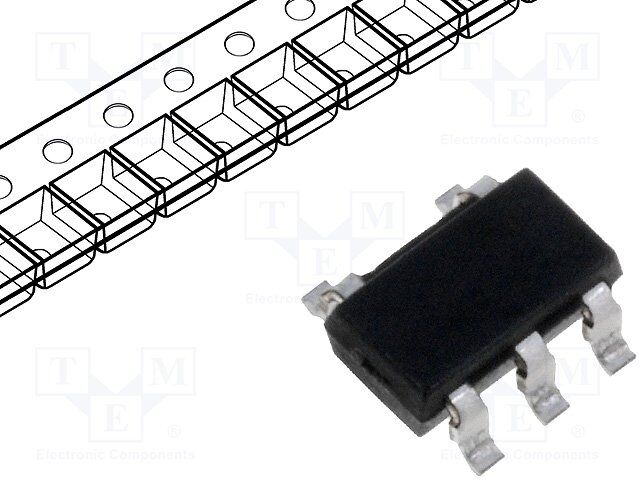
| 描述 | IC OPAMP GP 800KHZ SOT23-5运算放大器 - 运放 Single Low Power |
| 产品分类 | Linear - Amplifiers - Instrumentation, OP Amps, Buffer Amps集成电路 - IC |
| 品牌 | STMicroelectronics |
| 产品手册 | |
| 产品图片 |
|
| rohs | 符合RoHS无铅 / 符合限制有害物质指令(RoHS)规范要求 |
| 产品系列 | 放大器 IC,运算放大器 - 运放,STMicroelectronics TS321ILT- |
| 数据手册 | |
| 产品型号 | TS321ILT |
| 产品目录页面 | |
| 产品种类 | 运算放大器 - 运放 |
| 供应商器件封装 | SOT-23-5 |
| 共模抑制比—最小值 | 65 dB |
| 关闭 | No Shutdown |
| 其它名称 | 497-4061-6 |
| 其它有关文件 | http://www.st.com/web/catalog/sense_power/FM123/SC61/SS1378/PF65394?referrer=70071840http://www.st.com/web/catalog/sense_power/FM123/SC61/SS1614/PF65394?referrer=70071840 |
| 包装 | Digi-Reel® |
| 压摆率 | 0.4 V/µs |
| 双重电源电压 | +/- 3 V, +/- 5 V, +/- 9 V, +/- 12 V |
| 商标 | STMicroelectronics |
| 增益带宽生成 | 0.8 MHz |
| 增益带宽积 | 800kHz |
| 安装类型 | 表面贴装 |
| 安装风格 | SMD/SMT |
| 封装 | Reel |
| 封装/外壳 | SC-74A,SOT-753 |
| 封装/箱体 | SOT-23-5 |
| 工作温度 | -40°C ~ 125°C |
| 工作电源电压 | 3 V to 30 V, +/- 1.5 V to +/- 15 V |
| 工厂包装数量 | 3000 |
| 技术 | Bipolar |
| 放大器类型 | 通用 |
| 最大双重电源电压 | +/- 15 V |
| 最大工作温度 | + 125 C |
| 最小双重电源电压 | +/- 1.5 V |
| 最小工作温度 | - 40 C |
| 标准包装 | 1 |
| 电压-电源,单/双 (±) | 3 V ~ 30 V, ±1.5 V ~ 15 V |
| 电压-输入失调 | 500µV |
| 电流-电源 | 600µA |
| 电流-输入偏置 | 20nA |
| 电流-输出/通道 | 40mA |
| 电源电流 | 0.8 mA |
| 电路数 | 1 |
| 系列 | TS321 |
| 转换速度 | 0.4 V/us |
| 输入偏压电流—最大 | 150 nA |
| 输入参考电压噪声 | 40 nV |
| 输入补偿电压 | 4 mV |
| 输出电流 | 40 mA |
| 输出类型 | - |
| 通道数量 | 1 Channel |


- 商务部:美国ITC正式对集成电路等产品启动337调查
- 曝三星4nm工艺存在良率问题 高通将骁龙8 Gen1或转产台积电
- 太阳诱电将投资9.5亿元在常州建新厂生产MLCC 预计2023年完工
- 英特尔发布欧洲新工厂建设计划 深化IDM 2.0 战略
- 台积电先进制程称霸业界 有大客户加持明年业绩稳了
- 达到5530亿美元!SIA预计今年全球半导体销售额将创下新高
- 英特尔拟将自动驾驶子公司Mobileye上市 估值或超500亿美元
- 三星加码芯片和SET,合并消费电子和移动部门,撤换高东真等 CEO
- 三星电子宣布重大人事变动 还合并消费电子和移动部门
- 海关总署:前11个月进口集成电路产品价值2.52万亿元 增长14.8%


PDF Datasheet 数据手册内容提取
TS321 Low-power single operational amplifier Datasheet - production data Description The TS321 device is intended for cost-sensitive applications where space-saving is of great importance. This bipolar operational amplifier SOT23-5 (op amp) offers the benefits of a reduced (plasticpackage) component size (SOT23-5 package) with specifications that match (or are better than) Pinconnections(topview) industry standard devices (such as the popular LM358A, LM324, and other similar devices). The TS321 device has an input common mode range (Vicm) that includes ground and therefore can be employed in single supply applications. Features • Large output voltage swing − 0 to 3.5 V min (V = 5 V) CC • Low supply current: 500 µA • Low input bias current: 20 nA • Low input offset voltage − 2 mV max. for TS321A − 4 mV max. for TS321 • Wide power supply range − Single supply: 3 to 30 V − Dual supplies: ±1.5 to ±15 V • Stable with high capacitive loads November 2014 DocID6298 Rev 9 1/15 This is information on a product in full production. www.st.com
Contents TS321 Contents 1 Schematic diagram .......................................................................... 3 2 Absolute maximum ratings and operating conditions ................. 4 3 Electrical characteristics ................................................................ 5 4 Macromodel ..................................................................................... 8 4.1 Important note concerning this macromodel ..................................... 8 4.2 Macromodel code .............................................................................. 8 4.3 Electrical characteristics of the macromodel ................................... 10 5 Package information ..................................................................... 11 5.1 SOT23-5 package information ........................................................ 12 6 Ordering information ..................................................................... 13 7 Revision history ............................................................................ 14 2/15 DocID6298 Rev 9
TS321 Schematic diagram 1 Schematic diagram Figure 1: Schematic diagram t DocID6298 Rev 9 3/15
Absolute maximum ratings and operating TS321 conditions 2 Absolute maximum ratings and operating conditions Table 1: Absolute maximum ratings Symbol Parameter Value Unit VCC+ Supply voltage ±16 to 32 Vin Input voltage -0.3 to 32 V Vid Differential input voltage ±32 Output short-circuit duration (1) Infinite Iin Input current (2) 50 mA Tstg Storage temperature range -65 to 150 °C Tj Maximum junction temperature 150 Rthja Thermal resistance junction-to-ambient (3) 250 °C/W Rthjc Thermal resistance junction-to-case (3) 81 HBM: human body model (4) 500 ESD MM: machine model (5) 200 V CDM: charged device model (6) 1000 Notes: (1) Short-circuits from the output to VCC can cause excessive heating if VCC > 15 V. The maximum output current is approximately 40 mA independent of the magnitude of VCC. (2) This input current only exists when the voltage at any of the input leads is driven negative. It is due to the collector-base junction of the input PNP transistor becoming forward biased and thereby acting as input diodes clamps. In addition to this diode action, there is also NPN parasitic action on the IC chip. This transistor action can cause the output voltages of the op amp to go to the VCC voltage level (or to ground for a large overdrive) for the time during which an input is driven negative. This is not destructive and normal output is restored when the input voltage goes back above -0.3 V. (3) Short-circuits can cause excessive heating. Destructive dissipation can result from simultaneous short-circuits on all amplifiers. All values are typical. (4) Human body model: a 100 pF capacitor is charged to the specified voltage, then discharged through a 1.5 kΩ resistor between two pins of the device. This is done for all couples of connected pin combinations while the other pins are floating. (5) Machine model: a 200 pF capacitor is charged to the specified voltage, then discharged directly between two pins of the device with no external series resistor (internal resistor < 5 Ω). This is done for all couples of connected pin combinations while the other pins are floating. (6) Charged device model: all pins and the package are charged together to the specified voltage and then discharged directly to ground through only one pin. This is done for all pins. Table 2: Operating conditions Symbol Parameter Value Unit VCC+ Supply voltage 3 to 30 Input common mode voltage range Tamb = 25 °C 0 to (VCC+) - 1.5 V Vicm (VCC+ = 30 V) Tmin ≤ Tamb ≤ Tmax 0 to (VCC+) - 2 Toper Operating free air temperature range -40 to 125 °C 4/15 DocID6298 Rev 9
TS321 Electrical characteristics 3 Electrical characteristics Table 3: Electrical characteristics at VCC+ = 5 V, VCC- = ground, Vo = 1.4 V, Tamb = 25 °C (unless otherwise specified) Symbol Parameter Test conditions Min. Typ. Max. Unit TS321 0.5 4 TS321A 2 Vio Input offset voltage (1) mV Tmin ≤ Tamb ≤ Tmax, TS321 5 Tmin ≤ Tamb ≤ Tmax, TS321A 3 2 30 Iio Input offset current Tmin ≤ Tamb ≤ Tmax 50 nA 20 150 Iib Input bias current (2) Tmin ≤ Tamb ≤ Tmax 200 VCC+ = 15 V, RL = 2 kΩ, 50 100 Vo = 1.4 to 11.4 V Avd Large signal voltage gain Tmin ≤ Tamb ≤ Tmax, VCC+ = 15 V, 25 V/mV RL = 2 kΩ, Vo = 1.4 to 11.4 V SVR Srautipop ly voltage rejection Rs ≤ 10 kΩ, VCC+ = 5 to 30 V 65 110 dB VCC+ = 5 V 500 800 VCC+ = 30 V 600 900 ICC Supply current, no load Tmin ≤ Tamb ≤ Tmax, VCC+ = 5 V 600 900 µA Tmin ≤ Tamb ≤ Tmax, VCC+ = 30 V 1000 Common mode rejection CMR ratio Rs ≤ 10 kΩ 65 85 dB Isource Output current source Vid = 1 V, VCC+ = 15 V, Vo = 2 V 20 40 mA Vid = -1 V, VCC+ = 15 V, Vo = 2 V 10 20 mA Isink Output sink current Vid = -1 V, VCC+ = 15 V, Vo = 0.2 V 12 50 µA Io Short-circuit to ground VCC+ = 15 40 60 mA VCC+ = 30 V, RL = 2 kΩ 26 27 Tmin ≤ Tamb ≤ Tmax, VCC+ = 30 V, 25.5 RL = 2 kΩ VCC+ = 30 V, RL = 10 kΩ 27 28 VOH High-level output voltage Tmin ≤ Tamb ≤ Tmax, VCC+ = 30 V, 26.5 V RL = 10 kΩ VCC+ = 5 V, RL = 2 kΩ 3.5 Tmin ≤ Tamb ≤ Tmax, VCC+ = 5 V, 3 RL = 2 kΩ RL = 10 kΩ 5 15 VOL Low level output voltage mV Tmin ≤ Tamb ≤ Tmax, RL = 10 kΩ 20 VCC+ = 15 V, Vi = 0.5 to 3 V, SR Slew rate RL = 2 kΩ, CL = 100 pF, 0.4 V/µs unity gain DocID6298 Rev 9 5/15
Electrical characteristics TS321 Symbol Parameter Test conditions Min. Typ. Max. Unit VCC+ = 30 V, f = 100 kHz, GBP Gain bandwidth product Vin = 10 mV, RL = 2 kΩ, 0.8 MHz CL = 100 pF ϕm Phase margin 60 Degrees f = 1 kHz, Av = 20 dB, RL = 2 kΩ, THD Total harmonic distortion Vo = 2 Vpp, CL = 100 pF, 0.015 % VCC+ = 30 V nV ------------ en Evoqlutaivgael ent input noise fV =CC 1+ k=H 3z0, RV s = 100 Ω, 40 Hz Notes: (1)Vo = 1.4 V, Rs = 0 Ω, 5 V < (VCC+) < 30 V, 0 < Vicm < (VCC+) - 1.5 V (2) The direction of the input current is out of the IC. This current is essentially constant and independent of the state of the output. Therefore, there is no change in the load on the input lines. Figure 2: Current consumption versus temperature Figure 3: AC-coupled inverting amplifier V Figure 4: Non-inverting DC gain Figure 5: AC-coupled non-inverting amplifier 6/15 DocID6298 Rev 9
TS321 Electrical characteristics Figure 6: DC summing amplifier DocID6298 Rev 9 7/15
Macromodel TS321 4 Macromodel 4.1 Important note concerning this macromodel Please not the following points before using this macromodel • All models are a trade-off between accuracy and complexity (that is, simulation time) • Macromodels are not a substitute for breadboarding, rather, they confirm the validity of a design approach and help to select surrounding component values. • A macromodel emulates the nominal performance of a typical device within specified operating conditions (for example, temperature and supply voltage). Thus, the macromodel is often not as exhaustive as the datasheet. Its purpose is to illustrate the main parameters of the product. Data derived from macromodels used outside the specified conditions (for example, V CC and temperature) or even worse, outside of the device’s operating conditions (for example, V and Vicm), are not reliable in any way. CC 4.2 Macromodel code ** Standard Linear Ics Macromodels, 1993. ** CONNECTIONS : * 1 INVERTING INPUT * 2 NON-INVERTING INPUT * 3 OUTPUT * 4 POSITIVE POWER SUPPLY * 5 NEGATIVE POWER SUPPLY .SUBCKT TS321 1 2 3 4 5 *************************** .MODEL MDTH D IS=1E-8 KF=3.104131E-15 CJO=10F * INPUT STAGE CIP 2 5 1.000000E-12 CIN 1 5 1.000000E-12 EIP 10 5 2 5 1 EIN 16 5 1 5 1 RIP 10 11 2.600000E+01 RIN 15 16 2.600000E+01 RIS 11 15 2.003862E+02 DIP 11 12 MDTH 400E-12 DIN 15 14 MDTH 400E-12 VOFP 12 13 DC 0 VOFN 13 14 DC 0 IPOL 13 5 1.000000E-05 CPS 11 15 3.783376E-09 DINN 17 13 MDTH 400E-12 8/15 DocID6298 Rev 9
TS321 Macromodel VIN 17 5 0.000000e+00 DINR 15 18 MDTH 400E-12 VIP 4 18 2.000000E+00 FCP 4 5 VOFP 3.400000E+01 FCN 5 4 VOFN 3.400000E+01 FIBP 2 5 VOFN 2.000000E-03 FIBN 5 1 VOFP 2.000000E-03 * AMPLIFYING STAGE FIP 5 19 VOFP 3.600000E+02 FIN 5 19 VOFN 3.600000E+02 RG1 19 5 3.652997E+06 RG2 19 4 3.652997E+06 CC 19 5 6.000000E-09 DOPM 19 22 MDTH 400E-12 DONM 21 19 MDTH 400E-12 HOPM 22 28 VOUT 7.500000E+03 VIPM 28 4 1.500000E+02 HONM 21 27 VOUT 7.500000E+03 VINM 5 27 1.500000E+02 EOUT 26 23 19 5 1 VOUT 23 5 0 ROUT 26 3 20 COUT 3 5 1.000000E-12 DOP 19 25 MDTH 400E-12 VOP 4 25 2.242230E+00 DON 24 19 MDTH 400E-12 VON 24 5 7.922301E-01 .ENDS DocID6298 Rev 9 9/15
Macromodel TS321 4.3 Electrical characteristics of the macromodel Table 4: Electrical characteristics at VCC+ = 3 V, VCC- = 0 V, RL and CL connected to VCC/2, Tamb = 25 °C (unless otherwise specified) Symbol Conditions Value Unit Vio 0 mV Avd RL = 2 kΩ 100 V/mV ICC No load, per operator 300 µA Vicm 0 to 3.5 V VOH 3.5 V RL = 2 kΩ VOL 5 mV Ios Vo = 0 V 40 mA GBP 0.8 MHz SR RL = 2 kΩ, CL = 100 pF 0.4 V/µs ϕm 60 Degrees 10/15 DocID6298 Rev 9
TS321 Package information 5 Package information In order to meet environmental requirements, ST offers these devices in different grades of ECOPACK® packages, depending on their level of environmental compliance. ECOPACK® specifications, grade definitions and product status are available at: www.st.com. ECOPACK® is an ST trademark. DocID6298 Rev 9 11/15
Package information TS321 5.1 SOT23-5 package information Figure 7: SOT23-5 package mechanical drawing Table 5: SOT23-5 package mechanical data Dimensions Ref. Millimeters Inches Min. Typ. Max. Min. Typ. Max. A 0.90 1.20 1.45 0.035 0.047 0.057 A1 0.15 0.006 A2 0.90 1.05 1.30 0.035 0.041 0.051 B 0.35 0.40 0.50 0.014 0.016 0.020 C 0.09 0.15 0.20 0.004 0.006 0.008 D 2.80 2.90 3.00 0.110 0.114 0.118 D1 1.90 0.075 e 0.95 0.037 E 2.60 2.80 3.00 0.102 0.110 0.118 F 1.50 1.60 1.75 0.059 0.063 0.069 L 0.10 0.35 0.60 0.004 0.014 0.024 K 0 degrees 10 degrees 0 degrees 10 degrees 12/15 DocID6298 Rev 9
TS321 Ordering information 6 Ordering information Table 6: Order codes Temperature Order code Package Packaging Marking range TS321ILT K401 TS321AILT K402 -40 °C to 125 °C SOT23-5 Tape and reel TS321IYLT (1) K406 TS321AIYLT (1) K407 Notes: (1) Qualified and characterized according to AEC Q100 and Q003 or equivalent, advanced screening according to AEC Q001 and Q 002 or equivalent. DocID6298 Rev 9 13/15
Revision history TS321 7 Revision history Table 7: Document revision history Date Revision Changes 30-Jun-2001 1 Initial release PPAP references inserted in the datasheet, see order codes 04-Jul-2005 2 table. ESD protection inserted in Table 1: Absolute maximum ratings. Correction of errors in package names and markings in order 06-Sep-2005 3 codes table. Minor grammatical and formatting corrections. Missing PPAP references inserted, see order codes table. Thermal resistance junction to ambient and thermal resistance 12-Dec-2005 4 junction to case information added in Table 1: Absolute maximum ratings. Macromodel updated see Section 4: Macromodel. Added CDM value for SO-8 in Table 1: Absolute maximum ratings. Added Tj value in Table 1: Absolute maximum ratings. Macromodel updated see Section 4: Macromodel. 08-Nov-2007 5 Reformatted package information. Added footnote in Table 7: Order codes. Removed TS321IYD/IYDT and TS321AIYD/AIYDT order codes. Added CDM value for SOT23-5 package in Table 1: Absolute 08-Jul-2008 6 maximum ratings. 10-May-2010 7 Updated package information in Chapter 5. Qualified status of TS321IYLT and TS321AIYLT order codes 12-Sep-2010 8 in Table 7: Order codes, minor corrections throughout document. Removed SO8 package and all references to it Table 1: Absolute maximum ratings: Updated ESD, HBM data 12-Nov-2014 9 Section 5.1: updated SOT23-5 package information Table 7: Order codes: removed obsolete order codes (TS321ID, TS321IDT, TS321AID, TS321AIDT) 14/15 DocID6298 Rev 9
TS321 IMPORTANT NOTICE – PLEASE READ CAREFULLY STMicroelectronics NV and its subsidiaries (“ST”) reserve the right to make changes, corrections, enhancements, modifications, and improvements to ST products and/or to this document at any time without notice. Purchasers should obtain the latest relevant information on ST products before placing orders. ST products are sold pursuant to ST’s terms and conditions of sale in place at the time of order acknowledgement. Purchasers are solely responsible for the choice, selection, and use of ST products and ST assumes no liability for application assistance or the design of Purchasers’ products. No license, express or implied, to any intellectual property right is granted by ST herein. Resale of ST products with provisions different from the information set forth herein shall void any warranty granted by ST for such product. ST and the ST logo are trademarks of ST. All other product or service names are the property of their respective owners. Information in this document supersedes and replaces information previously supplied in any prior versions of this document. © 2014 STMicroelectronics – All rights reserved DocID6298 Rev 9 15/15
Mouser Electronics Authorized Distributor Click to View Pricing, Inventory, Delivery & Lifecycle Information: S TMicroelectronics: TS321ID TS321ILT TS321AILT TS321AID TS321AIDT TS321IDT TS321AIYLT TS321IYLT