ICGOO在线商城 > 集成电路(IC) > 线性 - 放大器 - 仪表,运算放大器,缓冲器放大器 > TS321IDBVT
 Datasheet下载
- 型号: TS321IDBVT
- 制造商: Texas Instruments
- 库位|库存: xxxx|xxxx
- 要求:
| 数量阶梯 | 香港交货 | 国内含税 |
| +xxxx | $xxxx | ¥xxxx |
查看当月历史价格
查看今年历史价格
TS321IDBVT产品简介:
ICGOO电子元器件商城为您提供TS321IDBVT由Texas Instruments设计生产,在icgoo商城现货销售,并且可以通过原厂、代理商等渠道进行代购。 TS321IDBVT价格参考。Texas InstrumentsTS321IDBVT封装/规格:线性 - 放大器 - 仪表,运算放大器,缓冲器放大器, 通用 放大器 1 电路 SOT-23-5。您可以下载TS321IDBVT参考资料、Datasheet数据手册功能说明书,资料中有TS321IDBVT 详细功能的应用电路图电压和使用方法及教程。
TS321IDBVT 是由 Texas Instruments 生产的低功耗、单通道双极型运算放大器,属于线性 - 放大器 - 仪表、运算放大器、缓冲器放大器类别。它具有多种应用场景,尤其适用于对功耗敏感和需要高精度信号处理的系统。

 应用场景:

1. 工业自动化与控制:
   - TS321IDBVT 可用于工业控制系统中的传感器信号调理。例如,在温度、压力、位移等传感器的应用中,该运放可以将微弱的传感器信号进行放大,同时保持低噪声特性,确保信号的准确性。
   - 在可编程逻辑控制器 (PLC) 中,TS321IDBVT 可以作为信号调理电路的一部分,处理来自各种传感器的输入信号,并将其转换为适合后续处理的形式。

2. 医疗设备:
   - 医疗设备如心电图机(ECG)、血压计、血糖仪等需要高精度的信号放大和处理。TS321IDBVT 的低噪声和低功耗特性使其非常适合这些应用,能够准确地放大生物电信号,确保诊断结果的可靠性。
   - 它还可以用于便携式医疗设备中,因为其低功耗特性有助于延长电池寿命。

3. 消费电子:
   - 在音频设备中,TS321IDBVT 可以用于前置放大器,放大来自麦克风或其它音源的微弱信号,同时保持良好的音质和低失真。
   - 在便携式电子产品如智能手机、平板电脑中,TS321IDBVT 的低功耗特点使其成为理想的选择,能够在不影响性能的情况下延长电池续航时间。

4. 汽车电子:
   - 汽车电子系统中,TS321IDBVT 可用于车载传感器信号处理,如胎压监测系统(TPMS)、倒车雷达等。其宽工作温度范围(-40°C 至 +125°C)使其能够在严苛的汽车环境中稳定工作。
   - 它还可以用于汽车音响系统中的信号放大,提供清晰的音频输出。

5. 测试与测量仪器:
   - 在示波器、万用表等测试仪器中,TS321IDBVT 可用于信号调理电路,确保测量结果的精确性和稳定性。其低偏置电流和低失调电压特性使得它在精密测量应用中表现出色。

总之,TS321IDBVT 凭借其低功耗、低噪声、高精度的特点,广泛应用于工业、医疗、消费电子、汽车等多个领域,特别是在需要高精度信号处理和低功耗的场合中表现尤为突出。
| 参数 | 数值 |
| -3db带宽 | - |
| 产品目录 | 集成电路 (IC)半导体 |
| 描述 | IC OPAMP GP 800KHZ SOT23-5运算放大器 - 运放 Lo-Pwr Single Op Amp |
| 产品分类 | Linear - Amplifiers - Instrumentation, OP Amps, Buffer Amps集成电路 - IC |
| 品牌 | Texas Instruments |
| 产品手册 | |
| 产品图片 |
|
| rohs | 符合RoHS无铅 / 符合限制有害物质指令(RoHS)规范要求 |
| 产品系列 | 放大器 IC,运算放大器 - 运放,Texas Instruments TS321IDBVT- |
| 数据手册 | |
| 产品型号 | TS321IDBVT |
| PCN设计/规格 | |
| 产品种类 | 运算放大器 - 运放 |
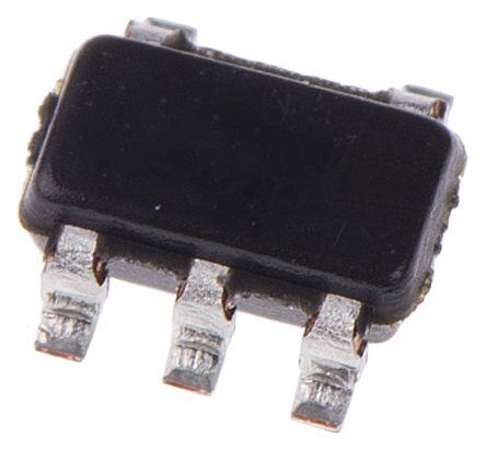
| 供应商器件封装 | SOT-23-5 |
| 共模抑制比—最小值 | 65 dB |
| 关闭 | No Shutdown |
| 其它名称 | 296-32590-6 |
| 包装 | Digi-Reel® |
| 单位重量 | 11.200 mg |
| 压摆率 | 0.4 V/µs |
| 双重电源电压 | +/- 3 V, +/- 5 V, +/- 9 V, +/- 12 V |
| 商标 | Texas Instruments |
| 增益带宽生成 | 0.8 MHz |
| 增益带宽积 | 800kHz |
| 安装类型 | 表面贴装 |
| 安装风格 | SMD/SMT |
| 封装 | Reel |
| 封装/外壳 | SC-74A,SOT-753 |
| 封装/箱体 | SOT-23-5 |
| 工作温度 | -40°C ~ 125°C |
| 工作电源电压 | 3 V to 30 V, +/- 1.5 V to +/- 15 V |
| 工厂包装数量 | 250 |
| 技术 | Bipolar |
| 放大器类型 | 通用 |
| 最大双重电源电压 | +/- 15 V |
| 最大工作温度 | + 125 C |
| 最小双重电源电压 | +/- 1.5 V |
| 最小工作温度 | - 40 C |
| 标准包装 | 1 |
| 电压-电源,单/双 (±) | 3 V ~ 30 V, ±1.5 V ~ 15 V |
| 电压-输入失调 | 500µV |
| 电流-电源 | 600µA |
| 电流-输入偏置 | 20nA |
| 电流-输出/通道 | 40mA |
| 电源电流 | 0.8 mA |
| 电路数 | 1 |
| 系列 | TS321 |
| 转换速度 | 0.4 V/us |
| 输入偏压电流—最大 | 150 nA |
| 输入参考电压噪声 | 50 nV |
| 输入补偿电压 | 4 mV |
| 输出电流 | 40 mA |
| 输出类型 | - |
| 通道数量 | 1 Channel |


- 商务部:美国ITC正式对集成电路等产品启动337调查
- 曝三星4nm工艺存在良率问题 高通将骁龙8 Gen1或转产台积电
- 太阳诱电将投资9.5亿元在常州建新厂生产MLCC 预计2023年完工
- 英特尔发布欧洲新工厂建设计划 深化IDM 2.0 战略
- 台积电先进制程称霸业界 有大客户加持明年业绩稳了
- 达到5530亿美元!SIA预计今年全球半导体销售额将创下新高
- 英特尔拟将自动驾驶子公司Mobileye上市 估值或超500亿美元
- 三星加码芯片和SET,合并消费电子和移动部门,撤换高东真等 CEO
- 三星电子宣布重大人事变动 还合并消费电子和移动部门
- 海关总署:前11个月进口集成电路产品价值2.52万亿元 增长14.8%


PDF Datasheet 数据手册内容提取
Product Order Technical Tools & Support & Folder Now Documents Software Community TS321 SLOS489D–DECEMBER2005–REVISEDMAY2018 TS321 Low-Power Single Operational Amplifier 1 Features 3 Description • WidePower-SupplyRange The TS321 is a bipolar operational amplifier for cost- 1 sensitive applications in which space savings are – SingleSupplyfrom3Vto30V important. – DualSupplyfrom±1.5Vto ±15V • LargeOutputVoltageSwingfrom DeviceInformation(1) 0Vto3.5V(Minimum)(V =5V) PARTNUMBER PACKAGE BODYSIZE(NOM) CC • LowSupplyCurrentat500μA(Typical) SOIC(8) 4.90mm×3.90mm TS321 • LowInputBiasCurrentat20nA(Typical) SOT-23(5) 2.90mm×1.60mm • StableWithHighCapacitiveLoads (1) For all available packages, see the orderable addendum at theendofthedatasheet. 2 Applications NC 1 8 NC • DesktopPCs IN– 2 7 V • HVAC:Heating,Ventilating,andAirConditioning CC+ • PortableMediaPlayers IN+ 3 6 OUT • Refrigerators V 4 5 NC CC– • WashingMachines:High-EndandLow-End OUT1 5 V CC+ V 2 CC– IN+3 4 IN– 1 An IMPORTANT NOTICE at the end of this data sheet addresses availability, warranty, changes, use in safety-critical applications, intellectualpropertymattersandotherimportantdisclaimers.PRODUCTIONDATA.
TS321 SLOS489D–DECEMBER2005–REVISEDMAY2018 www.ti.com Table of Contents 1 Features.................................................................. 1 7.2 FunctionalBlockDiagram.........................................8 2 Applications........................................................... 1 7.3 FeatureDescription...................................................8 3 Description............................................................. 1 7.4 DeviceFunctionalModes..........................................9 4 RevisionHistory..................................................... 2 8 ApplicationandImplementation........................ 10 8.1 ApplicationInformation............................................10 5 PinConfigurationandFunctions......................... 3 8.2 TypicalApplication .................................................10 6 Specifications......................................................... 4 9 PowerSupplyRecommendations...................... 12 6.1 AbsoluteMaximumRatings .....................................4 10 Layout................................................................... 12 6.2 ESDRatings..............................................................4 6.3 RecommendedOperatingConditions.......................4 10.1 LayoutGuidelines.................................................12 6.4 ThermalInformation:TS321.....................................4 10.2 LayoutExample....................................................12 6.5 ElectricalCharacteristics...........................................5 11 DeviceandDocumentationSupport................. 14 6.6 TypicalCharacteristics..............................................7 11.1 DocumentationSupport .......................................14 7 DetailedDescription.............................................. 8 11.2 Trademarks...........................................................14 7.1 Overview...................................................................8 11.3 ElectrostaticDischargeCaution............................14 11.4 Glossary................................................................14 4 Revision History ChangesfromRevisionC(April2015)toRevisionD Page • CorrectedSOICpackagepinoutquantityfrom"SOIC(14)"to"SOIC(8)"inDeviceInformationtable................................. 1 ChangesfromRevisionB(December2013)toRevisionC Page • AddedPinConfigurationandFunctionssection,ESDRatingstable,FeatureDescriptionsection,DeviceFunctional Modes,ApplicationandImplementationsection,PowerSupplyRecommendationssection,Layoutsection,Device andDocumentationSupportsection,andMechanical,Packaging,andOrderableInformationsection .............................. 1 2 SubmitDocumentationFeedback Copyright©2005–2018,TexasInstrumentsIncorporated ProductFolderLinks:TS321
TS321 www.ti.com SLOS489D–DECEMBER2005–REVISEDMAY2018 5 Pin Configuration and Functions DPackage 8-PinSOIC (TopView) NC 1 8 NC IN– 2 7 V CC+ IN+ 3 6 OUT V 4 5 NC CC– NC-nointernalconnection DBVPackage 5-PinSOT-23 (TopView) OUT1 5 V CC+ V 2 CC– IN+3 4 IN– PinFunctions PIN I/O DESCRIPTION NAME SOIC SOT-23 IN– 2 4 I Negativeinput IN+ 3 3 I Positiveinput 1 NC 5 — — Donotconnect 8 OUT 6 1 O Output V 4 2 — Negativesupply CC– V 7 5 — Positivesupply CC+ Copyright©2005–2018,TexasInstrumentsIncorporated SubmitDocumentationFeedback 3 ProductFolderLinks:TS321
TS321 SLOS489D–DECEMBER2005–REVISEDMAY2018 www.ti.com 6 Specifications 6.1 Absolute Maximum Ratings overoperatingfree-airtemperaturerange(unlessotherwisenoted)(1) MIN MAX UNIT Singlesupply 32 Supplyvoltage,V V CC Dualsupplies ±16 Differentialinputvoltage(2),V ±32 V ID Inputvoltagerange (3),V –0.3 32 V I Inputcurrent,I 50 mA IK Durationofoutputshortcircuittoground,t Unlimited short Operatingvirtualjunctiontemperature,T 150 °C J Storagetemperature,T –65 150 °C stg (1) StressesbeyondthoselistedunderAbsoluteMaximumRatingsmaycausepermanentdamagetothedevice.Thesearestressratings only,andfunctionaloperationofthedeviceattheseoranyotherconditionsbeyondthoseindicatedunderRecommendedOperating Conditionsisnotimplied.Exposuretoabsolute-maximum-ratedconditionsforextendedperiodsmayaffectdevicereliability. (2) DifferentialvoltagesareatIN+withrespecttoIN–. (3) InputvoltagesareatINwithrespecttoV . CC– 6.2 ESD Ratings VALUE UNIT Human-bodymodel(HBM),perANSI/ESDA/JEDECJS-001(1) ±2500 V(ESD) Electrostaticdischarge Charged-devicemodel(CDM),perJEDECspecificationJESD22- V C101(2) ±1500 (1) JEDECdocumentJEP155statesthat500-VHBMallowssafemanufacturingwithastandardESDcontrolprocess. (2) JEDECdocumentJEP157statesthat250-VCDMallowssafemanufacturingwithastandardESDcontrolprocess. 6.3 Recommended Operating Conditions MIN MAX UNIT Singlesupply 3 30 V Supplyvoltage V CC Dualsupply ±1.5 ±15 T Operatingfree-airtemperature –40 125 °C A 6.4 Thermal Information: TS321 TS321 THERMALMETRIC(1) (2)(3) D(SOIC) DBV(SOT-23) UNIT 5PINS 5PINS R Junction-to-ambientthermalresistance 97 206 °C/W θJA (1) Formoreinformationabouttraditionalandnewthermalmetrics,seetheSemiconductorandICPackageThermalMetricsapplication report. (2) MaximumpowerdissipationisafunctionofTJ(max),qJA,andT .Themaximumallowablepowerdissipationatanyallowableambient A temperatureisPD=[TJ(max)–TA]/qJA.Selectingthemaximumof150°Ccaneffectreliability. (3) ThepackagethermalimpedanceiscalculatedinaccordancewithJESD51-7. 4 SubmitDocumentationFeedback Copyright©2005–2018,TexasInstrumentsIncorporated ProductFolderLinks:TS321
TS321 www.ti.com SLOS489D–DECEMBER2005–REVISEDMAY2018 6.5 Electrical Characteristics V =5V,V =GND,V =1.4V(unlessotherwisenoted) CC+ CC– O PARAMETER TESTCONDITIONS MIN TYP MAX UNIT V Inputoffsetvoltage RS=0,5V<VCC+<30V TA=25°C 0.5 4 mV IO 0<VIC<(VCC+–1.5V) TA=Fullrange 5 T =25°C 2 30 A I Inputoffsetcurrent nA IO T =Fullrange 50 A T =25°C 20 150 I Inputbiascurrent(1) A nA IB T =Fullrange 200 A A Large-signaldifferential VCC=15V,RL=2kΩ TA=25°C 50 100 V/mV VD voltageamplification VO=1.4Vto11.4V TA=Fullrange 25 Common-modeinput TA=25°C 0 VCC+–1.5 VICR voltage(2) VCC=30V T =Fullrange 0 V –2 V A CC+ VCC=30V TA=25°C 26 27 RL=2kΩ TA=Fullrange 25.5 V High-leveloutputvoltage VCC=30V TA=25°C 27 28 V OH RL=10kΩ TA=Fullrange 26.5 VCC=5V TA=25°C 3.5 RL=2kΩ TA=Fullrange 3 T =25°C 5 15 A V Low-leveloutputvoltage R =10kΩ mV OL L T =Fullrange 20 A V =30V,V =10mV,R =2kΩ CC I L GBP Gainbandwidthproduct f=100kHz,C =100pF 0.8 MHz L T =25°C A V =15V,V =0.5Vto3V,R =2kΩ, CC I L SR Slewrate C =100pF,unitygain, 0.4 V/µs L T =25°C A φ Phasemargin T =25°C 60 ° m A R ≤10kΩ CMRR Common-moderejectionratio S 65 85 dB T =25°C A V =15V,V =2V,V =1V I Outputsourcecurrent CC O ID 20 40 mA SOURCE T =25°C A V =15V,V =1V CC ID V =2V 10 20 mA O T =25°C A I Outputsinkcurrent SINK V =15V,V =1V CC ID V =0.2V 12 50 µA O T =25°C A I Short-circuittoGND V =15V,T =25°C 40 60 mA O CC A SVR Supply-voltagerejectionratio V =5Vto30V,T =25°C 65 110 dB CC A V =5V CC 500 800 T =25°C,noload A V =30V CC 600 900 T =25°C,noload A I Totalsupplycurrent µA CC V =5V CC 600 900 T =fullrange,noload A V =30V CC 1000 T =fullrange,noload A V =30V,V =2V ,A =20dB THD Totalharmonicdistortion CC O pp V 0.015% R =2k,f=1kHz,C =100pF,T =25°C L L A (1) Thedirectionoftheinputcurrentisoutofthedevice.Thiscurrentessentiallyisconstant,independentofthestateoftheoutput,sono loadingchangeexistsontheinputlines. (2) Theinputcommon-modevoltageofeitherinputsignalshouldnotbeallowedtogonegativebymorethan0.3V.Theupperendofthe common-modevoltagerangeisV –1.5V,buteitherorbothinputscangoto32Vwithoutdamage. CC+ Copyright©2005–2018,TexasInstrumentsIncorporated SubmitDocumentationFeedback 5 ProductFolderLinks:TS321
TS321 SLOS489D–DECEMBER2005–REVISEDMAY2018 www.ti.com Electrical Characteristics (continued) V =5V,V =GND,V =1.4V(unlessotherwisenoted) CC+ CC– O PARAMETER TESTCONDITIONS MIN TYP MAX UNIT V =30V,f=1kHz,R =100Ω e Equivalentinputnoisevoltage CC S 50 N T =25°C A 6 SubmitDocumentationFeedback Copyright©2005–2018,TexasInstrumentsIncorporated ProductFolderLinks:TS321
TS321 www.ti.com SLOS489D–DECEMBER2005–REVISEDMAY2018 6.6 Typical Characteristics 45 0.8 40 0.7 35 0.6 s (nA) 2350 mA) 0.5 Bia20 C (0.4 put IC0.3 n15 I 0.2 10 5 Vcc = 5V 0.1 Vcc = 5V Vcc = 30V 0 0.0 –50 –25 0 25 50 75 100 125 –50 –25 0 25 50 75 100 125 Temperature (C) Temperature (C) C001 C001 Figure1.InputCurrentvsTemperature Figure2.SupplyCurrentvsTemperature 2.5 2.5 -40C 25C 2.0 2.0 125C V) + ( V) 1.5 Vcc1.5 VOL (1.0 e from 1.0 g a olt V 0.5 0.5 Iout = 3mA Iout = 15mA 0.0 0.0 0.01 0.1 1 10 –50 –25 0 25 50 75 100 125 IOL (mA) Temperature (C) C001 C001 Figure3.OutputSinkingCharacteristics Figure4.OutputSourcingCharacteristics 25 0 –5 20 –10 –15 A) 15 A) m m –20 put ( put ( –25 ut10 ut O O –30 5 –35 Vcc = 15V –40 Vcc = 15V 0 –45 –50 –25 0 25 50 75 100 125 –50 –25 0 25 50 75 100 125 Temperature (C) Temperature (C) C001 C001 Figure5.Short-CircuitCurrenttoSupply (1) Figure6.Short-CircuitCurrenttoGround (1) ShortcircuitsfromoutputstoVCCcancauseexcessiveheatingandeventualdestruction. Copyright©2005–2018,TexasInstrumentsIncorporated SubmitDocumentationFeedback 7 ProductFolderLinks:TS321
TS321 SLOS489D–DECEMBER2005–REVISEDMAY2018 www.ti.com 7 Detailed Description 7.1 Overview The TS321 is a single-channel operational amplifier. The device can handle a single supply between 3 V and 30 V or a dual-supply between ±1.5 V and ±15 V. Available in the small SOT-23 package, the TS321 is great for savingspaceinanyapplication. 7.2 Functional Block Diagram V CC IN– IN+ OUT 7.3 Feature Description 7.3.1 OperatingVoltage The TS321 can be powered from a single supply between 3 V and 30 V or a dual-supply between ±1.5 V and ±15V. 7.3.2 GainBandwidthProduct Gain bandwidth product is found by multiplying a measured bandwidth of the amplifier by the gain at which that bandwidthwasmeasured.TheTS321hasagainbandwidthof0.8MHz. 7.3.3 SlewRate The slew rate is the rate at which an operational amplifier can change the output when there is a change on the input.TheTS321hasa0.4-V/μsslewrate. 8 SubmitDocumentationFeedback Copyright©2005–2018,TexasInstrumentsIncorporated ProductFolderLinks:TS321
TS321 www.ti.com SLOS489D–DECEMBER2005–REVISEDMAY2018 Feature Description (continued) 7.3.4 InputCommon-ModeRange The valid common-mode range is from device ground pin to VCC – 1.5 V (VCC – 2 V across temperature). Inputs may exceed VCC up to the maximum VCC without device damage. At least one input must be in the valid input common-mode range for output to be correct phase. If both inputs exceed valid range then output phase is undefined. If either input is less than –0.3 V then input current must be limited to 1 mA and output phase is undefined. 7.3.5 StabilityWithHighCapacitiveLoads Operational amplifiers have reduced phase margin when there is a direct capacitance on the output. The stability is affected most when the amplifier is set to unity gain. Small signal response to a step input of 100 mV reveals the loop stability with a range of capacitors. See SLVA381 to correlate response waveform to phase margin. The responses at 1 nF or less indicate acceptable phase margin. The responses at 1 uF and above indicate good phasemargin. 100 pF 100 nF 1 µF 1 nF 10 µF 10 nF Figure7. Small-SignalResponse 7.4 Device Functional Modes The TS321 is powered on when the supply is connected. This device can operate as a single-supply operational amplifierordual-supplyamplifierdependingontheapplication. Copyright©2005–2018,TexasInstrumentsIncorporated SubmitDocumentationFeedback 9 ProductFolderLinks:TS321
TS321 SLOS489D–DECEMBER2005–REVISEDMAY2018 www.ti.com 8 Application and Implementation NOTE Information in the following applications sections is not part of the TI component specification, and TI does not warrant its accuracy or completeness. TI’s customers are responsible for determining suitability of components for their purposes. Customers should validateandtesttheirdesignimplementationtoconfirmsystemfunctionality. 8.1 Application Information The TS321 operational amplifier is useful in a wide range of signal conditioning applications. Inputs can be poweredbeforeVCCforflexibilityinmultiplesupplycircuits. 8.2 Typical Application A typical application for an operational amplifier in an inverting amplifier. This amplifier takes a positive voltage on the input, and makes the voltage a negative voltage of the same magnitude. In the same manner, the amplifiermakesnegativevoltagespositive. RF Vsup+ RI V OUT + V IN Vsup- Figure8. TypicalApplicationSchematic 8.2.1 DesignRequirements The supply voltage must be selected such that the supply voltage is larger than the input voltage range and output range. For instance, this application scales a signal of ±0.5 V to ±1.8 V. Setting the supply at ±12 V is sufficienttoaccommodatethisapplication. 8.2.2 DetailedDesignProcedure Determinethegainrequiredbytheinvertingamplifier: VOUT A V VIN (1) 1.8 A (cid:16)3.6 V (cid:16)0.5 (2) Once the desired gain is determined, select a value for RI or RF. Selecting a value in the kilohm range is desirable because the amplifier circuit uses currents in the milliamp range. This ensures the part does not draw too much current. This example selects 10 kΩ for RI which means 36 kΩ is be used for RF. This is determined byEquation3. RF A (cid:16) V RI (3) 10 SubmitDocumentationFeedback Copyright©2005–2018,TexasInstrumentsIncorporated ProductFolderLinks:TS321
TS321 www.ti.com SLOS489D–DECEMBER2005–REVISEDMAY2018 Typical Application (continued) 8.2.3 ApplicationCurve 2 VIN 1.5 VOUT 1 0.5 s t 0 ol V -0.5 -1 -1.5 -2 0 0.5 1 1.5 2 Time (ms) Figure9. InputandOutputVoltagesoftheInvertingAmplifier Copyright©2005–2018,TexasInstrumentsIncorporated SubmitDocumentationFeedback 11 ProductFolderLinks:TS321
TS321 SLOS489D–DECEMBER2005–REVISEDMAY2018 www.ti.com 9 Power Supply Recommendations TheTS321isspecifiedtooperatebetween3Vand30Voradualsupplybetween ±1.5Vand ±15V. CAUTION Supply voltages larger than 32 V for a single supply, or outside the range of ±16 V for a dual supply can permanently damage the device (see the Absolute Maximum Ratings ). Place 0.1-μF bypass capacitors close to the power-supply pins to reduce errors coupling in from noisy or high impedance power supplies. For more detailed information on bypass capacitor placement, see the Layout section. 10 Layout 10.1 Layout Guidelines Forbestoperationalperformanceofthedevice,usegoodPCBlayoutpractices,including: • Noise can propagate into analog circuitry through the power pins of the circuit as a whole, as well as the operational amplifier. Bypass capacitors are used to reduce the coupled noise by providing low impedance powersourceslocaltotheanalogcircuitry. – Connect low-ESR, 0.1-μF ceramic bypass capacitors between each supply pin and ground, placed as close to the device as possible. A single bypass capacitor from V+ to ground is applicable for single supplyapplications. • Separate grounding for analog and digital portions of circuitry is one of the simplest and most-effective methods of noise suppression. One or more layers on multilayer PCBs are usually devoted to ground planes. A ground plane helps distribute heat and reduces EMI noise pickup. Make sure to physically separate digital and analog grounds, paying attention to the flow of the ground current. For more detailed information, see SLOA089. • To reduce parasitic coupling, run the input traces as far away from the supply or output traces as possible. If it is not possible to keep them separate, it is much better to cross the sensitive trace perpendicular as opposedtoinparallelwiththenoisytrace. • Place the external components as close to the device as possible. Keeping RF and RG close to the inverting inputminimizesparasiticcapacitance,asshowninLayoutExample. • Keep the length of input traces as short as possible. Always remember that the input traces are the most sensitivepartofthecircuit. • Consider a driven, low-impedance guard ring around the critical traces. A guard ring can significantly reduce leakagecurrentsfromnearbytracesthatareatdifferentpotentials. 10.2 Layout Example RIN VIN + VOUT RG RF Figure10. OperationalAmplifierSchematicforNoninvertingConfiguration 12 SubmitDocumentationFeedback Copyright©2005–2018,TexasInstrumentsIncorporated ProductFolderLinks:TS321
TS321 www.ti.com SLOS489D–DECEMBER2005–REVISEDMAY2018 Layout Example (continued) Place components close to device and to each other to reduce parasitic errors Run the input traces as far away from the supply lines RF as possible NC NC VS+ Use low-ESR, ceramic RG bypass capacitor GND IN1(cid:237) VCC+ VIN IN1+ OUT RIN VCC(cid:237) NC GND Only needed for dual-supply operation GND VS- (or GND for single supply) VOUT Ground (GND) plane on another layer Figure11. OperationalAmplifierBoardLayoutforNoninvertingConfiguration Copyright©2005–2018,TexasInstrumentsIncorporated SubmitDocumentationFeedback 13 ProductFolderLinks:TS321
TS321 SLOS489D–DECEMBER2005–REVISEDMAY2018 www.ti.com 11 Device and Documentation Support 11.1 Documentation Support 11.1.1 RelatedDocumentation Formoreinformation,seethefollowing: • SimplifyingStabilityChecks • CircuitBoardLayoutTechniques 11.2 Trademarks Alltrademarksarethepropertyoftheirrespectiveowners. 11.3 Electrostatic Discharge Caution Thesedeviceshavelimitedbuilt-inESDprotection.Theleadsshouldbeshortedtogetherorthedeviceplacedinconductivefoam duringstorageorhandlingtopreventelectrostaticdamagetotheMOSgates. 11.4 Glossary SLYZ022—TIGlossary. Thisglossarylistsandexplainsterms,acronyms,anddefinitions. 14 SubmitDocumentationFeedback Copyright©2005–2018,TexasInstrumentsIncorporated ProductFolderLinks:TS321
PACKAGE OPTION ADDENDUM www.ti.com 11-Apr-2018 PACKAGING INFORMATION Orderable Device Status Package Type Package Pins Package Eco Plan Lead/Ball Finish MSL Peak Temp Op Temp (°C) Device Marking Samples (1) Drawing Qty (2) (6) (3) (4/5) TS321ID ACTIVE SOIC D 8 75 Green (RoHS CU NIPDAU Level-1-260C-UNLIM -40 to 125 SR321I & no Sb/Br) TS321IDBVR ACTIVE SOT-23 DBV 5 3000 Green (RoHS CU NIPDAU | CU SN Level-1-260C-UNLIM -40 to 125 (9C1G, 9C1S) & no Sb/Br) TS321IDBVRE4 ACTIVE SOT-23 DBV 5 3000 Green (RoHS CU NIPDAU Level-1-260C-UNLIM -40 to 125 9C1G & no Sb/Br) TS321IDBVRG4 ACTIVE SOT-23 DBV 5 3000 Green (RoHS CU NIPDAU Level-1-260C-UNLIM -40 to 125 9C1G & no Sb/Br) TS321IDBVT ACTIVE SOT-23 DBV 5 250 Green (RoHS CU NIPDAU | CU SN Level-1-260C-UNLIM -40 to 125 (9C1G, 9C1S) & no Sb/Br) TS321IDR ACTIVE SOIC D 8 2500 Green (RoHS CU NIPDAU Level-1-260C-UNLIM -40 to 125 SR321I & no Sb/Br) (1) The marketing status values are defined as follows: ACTIVE: Product device recommended for new designs. LIFEBUY: TI has announced that the device will be discontinued, and a lifetime-buy period is in effect. NRND: Not recommended for new designs. Device is in production to support existing customers, but TI does not recommend using this part in a new design. PREVIEW: Device has been announced but is not in production. Samples may or may not be available. OBSOLETE: TI has discontinued the production of the device. (2) RoHS: TI defines "RoHS" to mean semiconductor products that are compliant with the current EU RoHS requirements for all 10 RoHS substances, including the requirement that RoHS substance do not exceed 0.1% by weight in homogeneous materials. Where designed to be soldered at high temperatures, "RoHS" products are suitable for use in specified lead-free processes. TI may reference these types of products as "Pb-Free". RoHS Exempt: TI defines "RoHS Exempt" to mean products that contain lead but are compliant with EU RoHS pursuant to a specific EU RoHS exemption. Green: TI defines "Green" to mean the content of Chlorine (Cl) and Bromine (Br) based flame retardants meet JS709B low halogen requirements of <=1000ppm threshold. Antimony trioxide based flame retardants must also meet the <=1000ppm threshold requirement. (3) MSL, Peak Temp. - The Moisture Sensitivity Level rating according to the JEDEC industry standard classifications, and peak solder temperature. (4) There may be additional marking, which relates to the logo, the lot trace code information, or the environmental category on the device. (5) Multiple Device Markings will be inside parentheses. Only one Device Marking contained in parentheses and separated by a "~" will appear on a device. If a line is indented then it is a continuation of the previous line and the two combined represent the entire Device Marking for that device. Addendum-Page 1
PACKAGE OPTION ADDENDUM www.ti.com 11-Apr-2018 (6) Lead/Ball Finish - Orderable Devices may have multiple material finish options. Finish options are separated by a vertical ruled line. Lead/Ball Finish values may wrap to two lines if the finish value exceeds the maximum column width. Important Information and Disclaimer:The information provided on this page represents TI's knowledge and belief as of the date that it is provided. TI bases its knowledge and belief on information provided by third parties, and makes no representation or warranty as to the accuracy of such information. Efforts are underway to better integrate information from third parties. TI has taken and continues to take reasonable steps to provide representative and accurate information but may not have conducted destructive testing or chemical analysis on incoming materials and chemicals. TI and TI suppliers consider certain information to be proprietary, and thus CAS numbers and other limited information may not be available for release. In no event shall TI's liability arising out of such information exceed the total purchase price of the TI part(s) at issue in this document sold by TI to Customer on an annual basis. OTHER QUALIFIED VERSIONS OF TS321 : •Automotive: TS321-Q1 NOTE: Qualified Version Definitions: •Automotive - Q100 devices qualified for high-reliability automotive applications targeting zero defects Addendum-Page 2
PACKAGE MATERIALS INFORMATION www.ti.com 30-Apr-2018 TAPE AND REEL INFORMATION *Alldimensionsarenominal Device Package Package Pins SPQ Reel Reel A0 B0 K0 P1 W Pin1 Type Drawing Diameter Width (mm) (mm) (mm) (mm) (mm) Quadrant (mm) W1(mm) TS321IDBVR SOT-23 DBV 5 3000 180.0 8.4 3.23 3.17 1.37 4.0 8.0 Q3 TS321IDBVR SOT-23 DBV 5 3000 178.0 9.0 3.23 3.17 1.37 4.0 8.0 Q3 TS321IDBVRG4 SOT-23 DBV 5 3000 178.0 9.0 3.23 3.17 1.37 4.0 8.0 Q3 TS321IDBVT SOT-23 DBV 5 250 180.0 8.4 3.23 3.17 1.37 4.0 8.0 Q3 TS321IDBVT SOT-23 DBV 5 250 178.0 9.0 3.23 3.17 1.37 4.0 8.0 Q3 TS321IDR SOIC D 8 2500 330.0 12.4 6.4 5.2 2.1 8.0 12.0 Q1 PackMaterials-Page1
PACKAGE MATERIALS INFORMATION www.ti.com 30-Apr-2018 *Alldimensionsarenominal Device PackageType PackageDrawing Pins SPQ Length(mm) Width(mm) Height(mm) TS321IDBVR SOT-23 DBV 5 3000 202.0 201.0 28.0 TS321IDBVR SOT-23 DBV 5 3000 180.0 180.0 18.0 TS321IDBVRG4 SOT-23 DBV 5 3000 180.0 180.0 18.0 TS321IDBVT SOT-23 DBV 5 250 202.0 201.0 28.0 TS321IDBVT SOT-23 DBV 5 250 180.0 180.0 18.0 TS321IDR SOIC D 8 2500 340.5 338.1 20.6 PackMaterials-Page2
PACKAGE OUTLINE D0008A SOIC - 1.75 mm max height SCALE 2.800 SMALL OUTLINE INTEGRATED CIRCUIT C SEATING PLANE .228-.244 TYP [5.80-6.19] .004 [0.1] C A PIN 1 ID AREA 6X .050 [1.27] 8 1 2X .189-.197 [4.81-5.00] .150 NOTE 3 [3.81] 4X (0 -15 ) 4 5 8X .012-.020 B .150-.157 [0.31-0.51] .069 MAX [3.81-3.98] .010 [0.25] C A B [1.75] NOTE 4 .005-.010 TYP [0.13-0.25] 4X (0 -15 ) SEE DETAIL A .010 [0.25] .004-.010 0 - 8 [0.11-0.25] .016-.050 [0.41-1.27] DETAIL A (.041) TYPICAL [1.04] 4214825/C 02/2019 NOTES: 1. Linear dimensions are in inches [millimeters]. Dimensions in parenthesis are for reference only. Controlling dimensions are in inches. Dimensioning and tolerancing per ASME Y14.5M. 2. This drawing is subject to change without notice. 3. This dimension does not include mold flash, protrusions, or gate burrs. Mold flash, protrusions, or gate burrs shall not exceed .006 [0.15] per side. 4. This dimension does not include interlead flash. 5. Reference JEDEC registration MS-012, variation AA. www.ti.com
EXAMPLE BOARD LAYOUT D0008A SOIC - 1.75 mm max height SMALL OUTLINE INTEGRATED CIRCUIT 8X (.061 ) [1.55] SYMM SEE DETAILS 1 8 8X (.024) [0.6] SYMM (R.002 ) TYP [0.05] 5 4 6X (.050 ) [1.27] (.213) [5.4] LAND PATTERN EXAMPLE EXPOSED METAL SHOWN SCALE:8X SOLDER MASK SOLDER MASK METAL OPENING OPENING METAL UNDER SOLDER MASK EXPOSED METAL EXPOSED METAL .0028 MAX .0028 MIN [0.07] [0.07] ALL AROUND ALL AROUND NON SOLDER MASK SOLDER MASK DEFINED DEFINED SOLDER MASK DETAILS 4214825/C 02/2019 NOTES: (continued) 6. Publication IPC-7351 may have alternate designs. 7. Solder mask tolerances between and around signal pads can vary based on board fabrication site. www.ti.com
EXAMPLE STENCIL DESIGN D0008A SOIC - 1.75 mm max height SMALL OUTLINE INTEGRATED CIRCUIT 8X (.061 ) [1.55] SYMM 1 8 8X (.024) [0.6] SYMM (R.002 ) TYP [0.05] 5 4 6X (.050 ) [1.27] (.213) [5.4] SOLDER PASTE EXAMPLE BASED ON .005 INCH [0.125 MM] THICK STENCIL SCALE:8X 4214825/C 02/2019 NOTES: (continued) 8. Laser cutting apertures with trapezoidal walls and rounded corners may offer better paste release. IPC-7525 may have alternate design recommendations. 9. Board assembly site may have different recommendations for stencil design. www.ti.com
PACKAGE OUTLINE DBV0005A SOT-23 - 1.45 mm max height SCALE 4.000 SMALL OUTLINE TRANSISTOR C 3.0 2.6 0.1 C 1.75 1.45 B A 1.45 MAX PIN 1 INDEX AREA 1 5 2X 0.95 3.05 2.75 1.9 1.9 2 4 3 0.5 5X 0.3 0.15 0.2 C A B (1.1) TYP 0.00 0.25 GAGE PLANE 0.22 TYP 0.08 8 TYP 0.6 0 0.3 TYP SEATING PLANE 4214839/D 11/2018 NOTES: 1. All linear dimensions are in millimeters. Any dimensions in parenthesis are for reference only. Dimensioning and tolerancing per ASME Y14.5M. 2. This drawing is subject to change without notice. 3. Refernce JEDEC MO-178. 4. Body dimensions do not include mold flash, protrusions, or gate burrs. Mold flash, protrusions, or gate burrs shall not exceed 0.15 mm per side. www.ti.com
EXAMPLE BOARD LAYOUT DBV0005A SOT-23 - 1.45 mm max height SMALL OUTLINE TRANSISTOR PKG 5X (1.1) 1 5 5X (0.6) SYMM (1.9) 2 2X (0.95) 3 4 (R0.05) TYP (2.6) LAND PATTERN EXAMPLE EXPOSED METAL SHOWN SCALE:15X SOLDER MASK SOLDER MASK METAL UNDER METAL OPENING OPENING SOLDER MASK EXPOSED METAL EXPOSED METAL 0.07 MAX 0.07 MIN ARROUND ARROUND NON SOLDER MASK SOLDER MASK DEFINED DEFINED (PREFERRED) SOLDER MASK DETAILS 4214839/D 11/2018 NOTES: (continued) 5. Publication IPC-7351 may have alternate designs. 6. Solder mask tolerances between and around signal pads can vary based on board fabrication site. www.ti.com
EXAMPLE STENCIL DESIGN DBV0005A SOT-23 - 1.45 mm max height SMALL OUTLINE TRANSISTOR PKG 5X (1.1) 1 5 5X (0.6) SYMM 2 (1.9) 2X(0.95) 3 4 (R0.05) TYP (2.6) SOLDER PASTE EXAMPLE BASED ON 0.125 mm THICK STENCIL SCALE:15X 4214839/D 11/2018 NOTES: (continued) 7. Laser cutting apertures with trapezoidal walls and rounded corners may offer better paste release. IPC-7525 may have alternate design recommendations. 8. Board assembly site may have different recommendations for stencil design. www.ti.com
IMPORTANTNOTICEANDDISCLAIMER TIPROVIDESTECHNICALANDRELIABILITYDATA(INCLUDINGDATASHEETS),DESIGNRESOURCES(INCLUDINGREFERENCE DESIGNS),APPLICATIONOROTHERDESIGNADVICE,WEBTOOLS,SAFETYINFORMATION,ANDOTHERRESOURCES“ASIS” ANDWITHALLFAULTS,ANDDISCLAIMSALLWARRANTIES,EXPRESSANDIMPLIED,INCLUDINGWITHOUTLIMITATIONANY IMPLIEDWARRANTIESOFMERCHANTABILITY,FITNESSFORAPARTICULARPURPOSEORNON-INFRINGEMENTOFTHIRD PARTYINTELLECTUALPROPERTYRIGHTS. TheseresourcesareintendedforskilleddevelopersdesigningwithTIproducts.Youaresolelyresponsiblefor(1)selectingtheappropriate TIproductsforyourapplication,(2)designing,validatingandtestingyourapplication,and(3)ensuringyourapplicationmeetsapplicable standards,andanyothersafety,security,orotherrequirements.Theseresourcesaresubjecttochangewithoutnotice.TIgrantsyou permissiontousetheseresourcesonlyfordevelopmentofanapplicationthatusestheTIproductsdescribedintheresource.Other reproductionanddisplayoftheseresourcesisprohibited.NolicenseisgrantedtoanyotherTIintellectualpropertyrightortoanythird partyintellectualpropertyright.TIdisclaimsresponsibilityfor,andyouwillfullyindemnifyTIanditsrepresentativesagainst,anyclaims, damages,costs,losses,andliabilitiesarisingoutofyouruseoftheseresources. TI’sproductsareprovidedsubjecttoTI’sTermsofSale(www.ti.com/legal/termsofsale.html)orotherapplicabletermsavailableeitheron ti.comorprovidedinconjunctionwithsuchTIproducts.TI’sprovisionoftheseresourcesdoesnotexpandorotherwisealterTI’sapplicable warrantiesorwarrantydisclaimersforTIproducts. MailingAddress:TexasInstruments,PostOfficeBox655303,Dallas,Texas75265 Copyright©2019,TexasInstrumentsIncorporated