ICGOO在线商城 > 集成电路(IC) > PMIC - 稳压器 - DC DC 开关稳压器 > TPS84A20RVQT
 Datasheet下载
- 型号: TPS84A20RVQT
- 制造商: Texas Instruments
- 库位|库存: xxxx|xxxx
- 要求:
| 数量阶梯 | 香港交货 | 国内含税 |
| +xxxx | $xxxx | ¥xxxx |
查看当月历史价格
查看今年历史价格
TPS84A20RVQT产品简介:
ICGOO电子元器件商城为您提供TPS84A20RVQT由Texas Instruments设计生产,在icgoo商城现货销售,并且可以通过原厂、代理商等渠道进行代购。 TPS84A20RVQT价格参考。Texas InstrumentsTPS84A20RVQT封装/规格:PMIC - 稳压器 - DC DC 开关稳压器, 可调式 降压 开关稳压器 IC 正 0.6V 1 输出 10A 42-BQFN 裸露焊盘。您可以下载TPS84A20RVQT参考资料、Datasheet数据手册功能说明书,资料中有TPS84A20RVQT 详细功能的应用电路图电压和使用方法及教程。
TPS84A20RVQT 是 Texas Instruments(德州仪器)推出的一款集成式 DC-DC 开关稳压器模块,属于 PMIC(电源管理集成电路)中稳压器的类别。该器件集成了电感器、MOSFET 和控制电路,具备高集成度与小尺寸优势,适用于对空间和效率要求较高的应用。

其典型应用场景包括:

1. 工业自动化设备:用于为 PLC、传感器、工业控制器等提供高效稳定的电源转换。
2. 通信设备:如基站、路由器和交换机中的内部电源系统,支持宽输入电压范围,适应复杂环境。
3. 测试与测量仪器:为高精度仪表提供低噪声、高稳定性的电源解决方案。
4. 嵌入式系统:在 FPGA、DSP、ASIC 等处理器供电中广泛应用,支持多路输出配置。
5. 汽车电子系统:满足车载信息娱乐系统、ADAS 等对可靠性和效率有高要求的应用。

该模块具有过流、过温及欠压保护功能,工作温度范围宽,适合各种严苛环境。其简化设计和高可靠性使其成为多种中高端电子产品电源设计的理想选择。
| 参数 | 数值 |
| 产品目录 | 集成电路 (IC)半导体 |
| 描述 | IC REG BUCK SYNC ADJ 10A 42BQFN稳压器—开关式稳压器 2.95V-17V Input 10-A Sync Buck Pwr Sol |
| DevelopmentKit | TPS84A20EVM-001 |
| 产品分类 | |
| 品牌 | Texas Instruments |
| 产品手册 | |
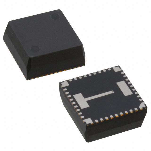
| 产品图片 |
|
| rohs | 符合RoHS无铅 / 符合限制有害物质指令(RoHS)规范要求 |
| 产品系列 | 电源管理 IC,稳压器—开关式稳压器,Texas Instruments TPS84A20RVQTECO-MODE™ |
| 数据手册 | |
| 产品型号 | TPS84A20RVQT |
| PWM类型 | - |
| 产品种类 | 稳压器—开关式稳压器 |
| 供应商器件封装 | 42-BQFN (10x10) |
| 其它名称 | 296-35993-2 |
| 包装 | 带卷 (TR) |
| 同步整流器 | 是 |
| 商标 | Texas Instruments |
| 安装类型 | 表面贴装 |
| 安装风格 | SMD/SMT |
| 封装 | Reel |
| 封装/外壳 | 42-BQFN 裸露焊盘 |
| 封装/箱体 | B3QFN-42 |
| 工作温度 | -40°C ~ 85°C |
| 工作温度范围 | - 40 C to + 85 C |
| 工厂包装数量 | 250 |
| 开关频率 | 200 kHz to 1.2 MHz |
| 拓扑结构 | Buck |
| 最大工作温度 | + 85 C |
| 最大输入电压 | 17 V |
| 最小工作温度 | - 40 C |
| 最小输入电压 | 2.95 V |
| 标准包装 | 250 |
| 电压-输入 | 2.95 V ~ 17 V |
| 电压-输出 | 0.6 V ~ 5.5 V |
| 电流-输出 | 10A |
| 电源电压-最小 | 2.95 V |
| 类型 | 降压(降压) |
| 系列 | TPS84A20 |
| 负载调节 | 0.2 % |
| 输出数 | 1 |
| 输出电压 | 600 mV to 5.5 V |
| 输出电流 | 10 A |
| 输出端数量 | 1 Output |
| 输出类型 | 可调式 |
| 频率-开关 | 200kHz ~ 1.2MHz |


- 商务部:美国ITC正式对集成电路等产品启动337调查
- 曝三星4nm工艺存在良率问题 高通将骁龙8 Gen1或转产台积电
- 太阳诱电将投资9.5亿元在常州建新厂生产MLCC 预计2023年完工
- 英特尔发布欧洲新工厂建设计划 深化IDM 2.0 战略
- 台积电先进制程称霸业界 有大客户加持明年业绩稳了
- 达到5530亿美元!SIA预计今年全球半导体销售额将创下新高
- 英特尔拟将自动驾驶子公司Mobileye上市 估值或超500亿美元
- 三星加码芯片和SET,合并消费电子和移动部门,撤换高东真等 CEO
- 三星电子宣布重大人事变动 还合并消费电子和移动部门
- 海关总署:前11个月进口集成电路产品价值2.52万亿元 增长14.8%


PDF Datasheet 数据手册内容提取
Product Order Technical Tools & Support & Reference Folder Now Documents Software Community Design TPS84A20 SLVSBC6C–MARCH2013–REVISEDDECEMBER2019 TPS84A20 2.95-V to 17-V Input, 10-A Synchronous Buck, Integrated Power Solution 1 Features 3 Description • Completeintegratedpowersolutionallows The TPS84A20 is an easy-to-use integrated power 1 solution that combines a 10-A DC/DC converter with smallfootprint,low-profiledesign power MOSFETs, an inductor, and passives into a • 10-mm×10-mm× 4.3-mmpackage low profile, QFN package. This total power solution • Efficienciesupto95% allows as few as three external components and • Eco-mode™/lightloadefficiency(LLE) eliminates the loop compensation and magnetics part selectionprocess. • Wide-outputvoltageadjust 0.6Vto5.5V,with1%referenceaccuracy The10-mm× 10-mm × 4.3-mm QFN package is easy to solder onto a printed circuit board and allows a • Supportsparalleloperationforhighercurrent compact point-of-load design. Achieves greater than • Optionalsplitpowerrailallows 95% efficiency and excellent power dissipation inputvoltagedownto2.95V capabilitywithathermal impedance of 13.3°C/W. The • Adjustableswitchingfrequency TPS84A20 offers the flexibility and the feature-set of (200kHzto1.2MHz) a discrete point-of-load design and is ideal for powering a wide range of ICs and systems. • Synchronizestoanexternalclock Advanced packaging technology affords a robust and • Provides180° out-of-phaseclocksignal reliable power solution compatible with standard QFN • Adjustableslow-start mountingandtestingtechniques. • Outputvoltagesequencing/tracking SPACER • Power-goodoutput SPACER • Programmableundervoltagelockout(UVLO) SPACER • Overcurrentandovertemperatureprotection SPACER • Prebiasoutputstart-up • Operatingtemperaturerange:–40°Cto+85°C SPACER • Enhancedthermalperformance:13.3°C/W SPACER • MeetsEN55022ClassBEmissions SPACER 2 Applications SPACER • Broadbandandcommunicationsinfrastructure SPACER • Automatedtestandmedicalequipment SimplifiedApplication • CompactPCI/PCIexpress/PXIexpress • DSPandFPGApoint-of-loadapplications VIN PVIN ISHARE 100 95 VIN VOUT 90 CIN VOUT 85 ency (%) 7850 Vout = 2.5 V TPS84SAE2N0SE+ COUT Effici 70 Fsw = 750 kHz 65 PVIN = 3.3 V, VIN = 5 V SYNC_OUT 60 PWRGD PVIN = VIN = 5 V 55 INH/UVLO PVIN = VIN = 12 V 50 VADJ 0 1 2 3 4 5 6 7 8 9 10 SS/TR Output Current (A) C001 RT/CLK RSET STSEL AGND PGND RRT 1 An IMPORTANT NOTICE at the end of this data sheet addresses availability, warranty, changes, use in safety-critical applications, intellectualpropertymattersandotherimportantdisclaimers.PRODUCTIONDATA.
TPS84A20 SLVSBC6C–MARCH2013–REVISEDDECEMBER2019 www.ti.com 4 Revision History NOTE:Pagenumbersforpreviousrevisionsmaydifferfrompagenumbersinthecurrentversion. ChangesfromRevisionB(April2018)toRevisionC Page • AddedV RangevaluesunderdifferentI conditionsinTable9.................................................................................. 24 OUT OUT ChangesfromRevisionA(June2017)toRevisionB Page • AddedtopnaviconforTIreferencedesign .......................................................................................................................... 1 • IncreasedthepeakreflowtemperatureandmaximumnumberofreflowstoJEDECspecificationforimproved manufacturability.................................................................................................................................................................... 3 • AddedMechanical,Packaging,andOrderableInformationsection.................................................................................... 29 ChangesfromOriginal(MARCH2013)toRevisionA Page • Addedpeakreflowandmaximumnumberofreflowsinformation ........................................................................................ 3 • AddedParallelOperationsection......................................................................................................................................... 19 2 SubmitDocumentationFeedback Copyright©2013–2019,TexasInstrumentsIncorporated ProductFolderLinks:TPS84A20
TPS84A20 www.ti.com SLVSBC6C–MARCH2013–REVISEDDECEMBER2019 Table1.OrderingInformation Forthemostcurrentpackageandorderinginformation,seethePackageOptionAddendumattheendofthisdatasheet,orsee theTIwebsiteatwww.ti.com. 5 Specifications 5.1 Absolute Maximum Ratings(1) overoperatingtemperaturerange(unlessotherwisenoted) MIN MAX UNIT VIN,PVIN –0.3 20 V InputVoltage INH/UVLO,PWRGD,RT/CLK,SENSE+ –0.3 6 V ILIM,VADJ,SS/TR,STSEL,SYNC_OUT,ISHARE,OCP_SEL –0.3 3 V PH –1.0 20 V OutputVoltage PH10nsTransient –3.0 20 V VOUT –0.3 6 V RT/CLK,INH/UVLO ±100 µA SourceCurrent PH currentlimit A PH currentlimit A SinkCurrent PVIN currentlimit A PWRGD –0.1 2 mA OperatingJunctionTemperature –40 125(2) °C StorageTemperature –65 150 °C PeakReflowCaseTemperature(3)(4) 245 °C MaximumNumberofReflowsAllowed(3)(4) 3 MechanicalShock Mil-STD-883D,Method2002.3,1msec,1/2sine,mounted 1500 G MechanicalVibration Mil-STD-883D,Method2007.2,20-2000Hz 20 (1) Stressesbeyondthoselistedunderabsolutemaximumratingsmaycausepermanentdamagetothedevice.Thesearestressratings only,andfunctionaloperationofthedeviceattheseoranyotherconditionsbeyondthoseindicatedunderrecommendedoperating conditionsisnotimplied.Exposuretoabsolute-maximum-ratedconditionsforextendedperiodsmayaffectdevicereliability. (2) SeethetemperaturederatingcurvesintheTypicalCharacteristicssectionforthermalinformation. (3) Forsolderingspecifications,refertotheSolderingRequirementsforBQFNPackagesapplicationnote. (4) Deviceswithadatecodepriortoweek142018(1814)haveapeakreflowcasetemperatureof240°Cwithamaximumofonereflow. 5.2 Recommended Operating Conditions overoperatingfree-airtemperaturerange(unlessotherwisenoted) MIN NOM MAX UNIT PV InputSwitchingVoltage 2.95 17 V IN V InputBiasVoltage 4.5 17 V IN V OutputVoltage 0.6 5.5 V OUT f SwitchingFrequency 200 1200 kHz SW 5.3 Package Specifications TPS84A20 UNIT Weight 1.45grams Flammability MeetsUL94V-O MTBFCalculatedreliability PerBellcoreTR-332,50%stress,T =40°C,groundbenign 37.4MHrs A Copyright©2013–2019,TexasInstrumentsIncorporated SubmitDocumentationFeedback 3 ProductFolderLinks:TPS84A20
TPS84A20 SLVSBC6C–MARCH2013–REVISEDDECEMBER2019 www.ti.com 5.4 Electrical Characteristics Over–40°Cto85°Cfree-airtemperature,PV =V =12V,V =1.8V,I =10A, IN IN OUT OUT C =0.1µF+2x22µFceramic+100µFbulk,C =4x47µFceramic(unlessotherwisenoted) IN OUT PARAMETER TESTCONDITIONS MIN TYP MAX UNIT IOUT Outputcurrent TA=85°C,naturalconvection 0(1) 10 A VIN Inputbiasvoltagerange Overoutputcurrentrange 4.5 17 V PVIN Inputswitchingvoltagerange Overoutputcurrentrange 2.95(2) 17(3) V VINIncreasing 4.0 4.5 UVLO VINUndervoltagelockout V VINDecreasing 3.5 3.85 VOUT(adj) Outputvoltageadjustrange Overoutputcurrentrange 0.6 5.5 V Set-pointvoltagetolerance TA=25°C,IOUT=0A ±1%(4) Temperaturevariation –40°C≤TA≤+85°C,IOUT=0A ±0.2% VOUT Lineregulation Overinputvoltagerange ±0.1% Loadregulation Overoutputcurrentrange ±0.2% Totaloutputvoltagevariation Includesset-point,line,load,andtemperaturevariation ±1.5%(4) VOUT=5.0V,fSW=1MHz 93% VOUT=3.3V,fSW=750kHz 92% VOUT=2.5V,fSW=750kHz 90% PIOV=IN5=AVIN=12V VOUT=1.8V,fSW=500kHz 89% VOUT=1.2V,fSW=300kHz 86% VOUT=0.9V,fSW=250kHz 84% η Efficiency VOUT=0.6V,fSW=200kHz 81% PVIN=VIN=5V VOUT=3.3V,fSW=750kHz 94% IO=5A VOUT=2.5V,fSW=750kHz 93% VOUT=1.8V,fSW=500kHz 92% VOUT=1.2V,fSW=300kHz 89% VOUT=0.9V,fSW=250kHz 87% VOUT=0.6V,fSW=200kHz 83% Outputvoltageripple 20MHzbandwidth 14 mVP-P ILIMpinopen 15 A ILIM Currentlimitthreshold ILIMpintoAGND 12 A 1.0A/µsloadstepfrom Recoverytime 100 µs Transientresponse 25to75%IOUT(max) VOUTover/undershoot 80 mV InhibitHighVoltage 1.3 open(5) VINH Inhibitthresholdvoltage V InhibitLowVoltage -0.3 1.1 INHInputcurrent VINH<1.1V -1.15 μA IINH INHHysteresiscurrent VINH>1.3V -3.3 μA II(stby) Inputstandbycurrent INHpintoAGND 2 10 µA Good 95% VOUTrising Fault 108% PWRGDThresholds PowerGood Fault 91% VOUTfalling Good 104% PWRGDLowVoltage I(PWRGD)=0.5mA 0.3 V fSW Switchingfrequency RRT=169kΩ 400 500 600 kHz fCLK Synchronizationfrequency 200 1200 kHz VCLK-H CLKHigh-Level 2.0 5.5 V CLKControl VCLK-L CLKLow-Level 0.5 V DCLK CLKDutyCycle 20 50 80 % (1) SeeLightLoadEfficiency(LLE)sectionformoreinformationforoutputvoltages<1.5V. (2) TheminimumP is2.95Vor(V +0.7V),whicheverisgreater.SeeTable9formoredetails. VIN OUT (3) ThemaximumPV voltageis17Vor(22xV ),whicheverisless.SeeTable9formoredetails. IN OUT (4) Thestatedlimitoftheset-pointvoltagetoleranceincludesthetoleranceofboththeinternalvoltagereferenceandtheinternal adjustmentresistor.TheoveralloutputvoltagetolerancewillbeaffectedbythetoleranceoftheexternalR resistor. SET (5) ValuewhennovoltagedividerispresentattheINH/UVLOpin.Thispinhasaninternalpull-up.Ifitisleftopen,thedeviceoperates wheninputpowerisapplied.Asmall,low-leakageMOSFETisrecommendedforcontrol.DonottiethispintoVIN. 4 SubmitDocumentationFeedback Copyright©2013–2019,TexasInstrumentsIncorporated ProductFolderLinks:TPS84A20
TPS84A20 www.ti.com SLVSBC6C–MARCH2013–REVISEDDECEMBER2019 Electrical Characteristics (continued) Over–40°Cto85°Cfree-airtemperature,PV =V =12V,V =1.8V,I =10A, IN IN OUT OUT C =0.1µF+2x22µFceramic+100µFbulk,C =4x47µFceramic(unlessotherwisenoted) IN OUT PARAMETER TESTCONDITIONS MIN TYP MAX UNIT Thermalshutdown 175 °C ThermalShutdown Thermalshutdownhysteresis 10 °C Ceramic 44(6) CIN Externalinputcapacitance Non-ceramic 100(6) µF Ceramic 47(7) 200 1500 µF COUT Externaloutputcapacitance Non-ceramic 220(7) 5000(8) Equivalentseriesresistance(ESR) 35 mΩ (6) Aminimumof44µFofexternalceramiccapacitanceisrequiredacrosstheinput(VINandPVINconnected)forproperoperation.An additional100µFofbulkcapacitanceisrecommended.Itisalsorecommendedtoplacea0.1-µFceramiccapacitordirectlyacrossthe PVINandPGNDpinsofthedevice.Locatetheinputcapacitanceclosetothedevice.WhenoperatingwithsplitVINandPVINrails, place4.7µFofceramiccapacitancedirectlyattheVINpin.SeeTable6formoredetails. (7) Theamountofrequiredoutputcapacitancevariesdependingontheoutputvoltage(seeTable5).Theamountofrequiredcapacitance mustincludeatleast1x47µFceramiccapacitor.Locatethecapacitanceclosetothedevice.Addingadditionalcapacitanceclosetothe loadimprovestheresponseoftheregulatortoloadtransients.SeeTable5andTable6moredetails. (8) Themaximumoutputcapacitanceof5000µFincludesthecombinationofbothceramicandnon-ceramiccapacitors. 5.5 Thermal Information TPS84A20 THERMALMETRIC(1) RVQ42 UNIT 42PINS θ Junction-to-ambientthermalresistance(2) 13.3 JA ψ Junction-to-topcharacterizationparameter(3) 1.6 °C/W JT ψ Junction-to-boardcharacterizationparameter(4) 5.3 JB (1) Formoreinformationabouttraditionalandnewthermalmetrics,seetheICPackageThermalMetricsApplicationReport. (2) Thejunction-to-ambientthermalresistance,θ ,appliestodevicessoldereddirectlytoa100-mmx100-mmdouble-sidedPCBwith JA 2oz.copperandnaturalconvectioncooling.Additionalairflowreducesθ . JA (3) Thejunction-to-topcharacterizationparameter,ψ ,estimatesthejunctiontemperature,T,ofadeviceinarealsystem,usinga JT J proceduredescribedinJESD51-2A(sections6and7).T =ψ *Pdis+T ;wherePdisisthepowerdissipatedinthedeviceandT is J JT T T thetemperatureofthetopofthedevice. (4) Thejunction-to-boardcharacterizationparameter,ψ ,estimatesthejunctiontemperature,T,ofadeviceinarealsystem,usinga JB J proceduredescribedinJESD51-2A(sections6and7).T =ψ *Pdis+T ;wherePdisisthepowerdissipatedinthedeviceandT is J JB B B thetemperatureoftheboard1mmfromthedevice. Copyright©2013–2019,TexasInstrumentsIncorporated SubmitDocumentationFeedback 5 ProductFolderLinks:TPS84A20
TPS84A20 SLVSBC6C–MARCH2013–REVISEDDECEMBER2019 www.ti.com 6 Device Information FunctionalBlockDiagram OCP_SEL ILIM OCP Shutdown INH/UVLO Logic PWRGD VIN Thermal VIN Shutdown UVLO PWRGD PVIN SENSE+ Logic VADJ SS/TR + PH + Comp VREF Power Stage VOUT STSEL and Current Control ISHARE Share Logic SYNC_OUT Oscillator PGND with PLL RT/CLK AGND TPS84A20 6 SubmitDocumentationFeedback Copyright©2013–2019,TexasInstrumentsIncorporated ProductFolderLinks:TPS84A20
TPS84A20 www.ti.com SLVSBC6C–MARCH2013–REVISEDDECEMBER2019 Table2.PinDescriptions TERMINAL DESCRIPTION NAME NO. 2 Zerovoltreferencefortheanalogcontrolcircuit.Thesepinsarenotconnectedtogetherinternaltothe AGND deviceandmustbeconnectedtooneanotherusinganAGNDplaneofthePCB.Thesepinsareassociated 23 withtheinternalanalogground(AGND)ofthedevice.SeeLayoutConsiderations. 20 21 Thisisthereturncurrentpathforthepowerstageofthedevice.Connectthesepinstotheloadandtothe PGND 31 bypasscapacitorsassociatedwithPVINandVOUT. 32 33 Inputbiasvoltagepin.Suppliesthecontrolcircuitryofthepowerconverter.Connectthispintotheinputbias VIN 3 supply.ConnectbypasscapacitorsbetweenthispinandPGND. 1 11 Inputswitchingvoltage.Suppliesvoltagetothepowerswitchesoftheconverter.Connectthesepinstothe PVIN 12 inputsupply.ConnectbypasscapacitorsbetweenthesepinsandPGND. 39 40 34 35 36 Outputvoltage.Thesepinsareconnectedtotheinternaloutputinductor.Connectthesepinstotheoutput VOUT 37 loadandconnectexternalbypasscapacitorsbetweenthesepinsandPGND. 38 41 10 13 14 15 Phaseswitchnode.Thesepinsmustbeconnectedtooneanotherusingasmallcopperislandunderthe PH 16 deviceforthermalrelief.Donotplaceanyexternalcomponentonthesepinsortiethemtoapinofanother function. 17 18 19 42 5 Donotconnect.DonotconnectthesepinstoAGND,toanotherDNCpin,ortoanyothervoltage.These DNC 9 pinsareconnectedtointernalcircuitry.Eachpinmustbesolderedtoanisolatedpad. 24 Currentsharepin.ConnectthispintootherTPS84A20devicesISHAREpinwhenparallelingmultiple ISHARE 25 TPS84A20devices.Whenunused,treatthispinasaDoNotConnect(DNC)andleaveitisolatedfromall othersignalsorground. Overcurrentprotectionselectpin.Leavethispinopenforhiccupmodeoperation.ConnectthispintoAGND OCP_SEL 4 forcycle-by-cycleoperation.SeeOvercurrentProtectionformoredetails. Currentlimitpin.Leavethispinopenforfullcurrentlimitthreshold.ConnectthispintoAGNDtoreducethe ILIM 6 currentlimitthresholdbyapproximately20%. SYNC_OUT 7 Synchronizationoutputpin.Providesa180°out-of-phaseclocksignal. PowerGoodflagpin.Thisopendrainoutputassertslowiftheoutputvoltageismorethanapproximately PWRGD 8 ±6%outofregulation.Apullupresistorisrequired. Thispinisconnectedtoaninternalfrequencysettingresistorwhichsetsthedefaultswitchingfrequency.An RT/CLK 22 externalresistorcanbeconnectedfromthispintoAGNDtoincreasethefrequency.Thispincanalsobe usedtosynchronizetoanexternalclock. VADJ 26 ConnectingaresistorbetweenthispinandAGNDsetstheoutputvoltage. Remotesenseconnection.ThispinmustbeconnectedtoVOUTattheloadoratthedevicepins.Connect SENSE+ 27 thispintoVOUTattheloadforimprovedregulation. Copyright©2013–2019,TexasInstrumentsIncorporated SubmitDocumentationFeedback 7 ProductFolderLinks:TPS84A20
TPS84A20 SLVSBC6C–MARCH2013–REVISEDDECEMBER2019 www.ti.com Table2.PinDescriptions(continued) TERMINAL DESCRIPTION NAME NO. Slow-startandtrackingpin.Connectinganexternalcapacitortothispinadjuststheoutputvoltagerisetime. SS/TR 28 Avoltageappliedtothispinallowsfortrackingandsequencingcontrol. Slow-startortrackfeatureselect.ConnectthispintoAGNDtoenabletheinternalSScapacitor.Leavethis STSEL 29 pinopentoenabletheTRfeature. InhibitandUVLOadjustpin.Useanopendrainoropencollectorlogicdevicetogroundthispintocontrol INH/UVLO 30 theINHfunction.Aresistordividerbetweenthispin,AGND,andPVIN/VINsetstheUVLOvoltage. RVQPACKAGE (TOPVIEW) T T T T T D D N N U U U U U N N VI VI O O O O O G G P P V V V V V P P PVIN 1 40 39 38 37 36 35 34 33 32 31 PGND AGND 2 41 VOUT 30 INH/UVLO VIN 3 29 STSEL OCP_SEL 4 28 SS/TR DNC 5 27 SENSE+ ILIM 6 26 VADJ SYNC_OUT 7 25 ISHARE PWRGD 8 24 DNC DNC 9 23 AGND PH 10 42 PH 22 RT/CLK PVIN 11 12 13 14 15 16 17 18 19 20 21 PGND N H H H H H H H D VI P P P P P P P N P G P 8 SubmitDocumentationFeedback Copyright©2013–2019,TexasInstrumentsIncorporated ProductFolderLinks:TPS84A20
TPS84A20 www.ti.com SLVSBC6C–MARCH2013–REVISEDDECEMBER2019 7 Typical Characteristics (PVIN = VIN = 12 V) 100 30 Vo = 5.0V, fsw = 1MHz Vo = 3.3V, fsw = 750kHz 90 V) 25 Vo = 2.5V, fsw = 750kHz m Vo = 1.8V, fsw = 500kHz Efficiency (%) 678000 VVVooo === 532...035VVV,,, fffssswww === 177M5500HkkzHH zz put Ripple Voltage (1250 VVoo == 10..29VV,, ffssww == 320500kkHHzz 50 Vo = 1.8V, fsw = 500kHz Out10 Vo = 1.2V, fsw = 300kHz Vo = 0.9V, fsw = 250kHz 40 5 0 1 2 3 4 5 6 7 8 9 10 0 2 4 6 8 10 Output Current (A) C001 Output Current (A) C004 Figure1.EfficiencyversusOutputCurrent Figure2.VoltageRippleversusOutputCurrent 5.0 40 120 Vo = 5.0V, fsw = 1MHz 4.5 Vo = 3.3V, fsw = 750kHz 30 90 Vo = 2.5V, fsw = 750kHz 4.0 W) Vo = 1.8V, fsw = 500kHz 20 60 er Dissipation (2233....0505 VVoo == 10..29VV,, ffssww == 320500kkHHzz Gain (dB) –11000 03– 03 0 (cid:131)Phase () ow1.5 –20 –60 P 1.0 Gain –30 –90 0.5 Phase –40 –120 0.0 1000 10k 100k 400k 0 2 4 6 8 10 Output Current (A) C004 Frequency (Hz) C006 Figure4.V =1.8V,I =10A,C =200µFCeramic, Figure3.PowerDissipationversusOutputCurrent OUT OUT OUT1 f =500kHz SW 90 90 80 80 C) C) (cid:131)e (70 (cid:131)e (70 ur ur erat60 erat60 p p m m e50 e50 nt T Airflow = 0 LFM nt T Airflow = 200 LFM bie40 9R(cid:3)(cid:148)(cid:3)(cid:20)(cid:17)(cid:27)9(cid:15)(cid:3)IVZ(cid:3) (cid:3)(cid:24)(cid:19)(cid:19)N+] bie40 9R(cid:3)(cid:148)(cid:3)(cid:20)(cid:17)(cid:27)9(cid:15)(cid:3)IVZ(cid:3) (cid:3)(cid:24)(cid:19)(cid:19)N+] m m A Vo = 2.5V, fsw = 750kHz A Vo = 2.5V, fsw = 750kHz 30 30 Vo = 3.3V, fsw = 750kHz Vo = 3.3V, fsw = 750kHz Vo = 5.0V, fsw = 1MHz Vo = 5.0V, fsw = 1MHz 20 20 0 2 4 6 8 10 0 2 4 6 8 10 Output Current (A) C001 Output Current (A) C001 Figure5.SafeOperatingArea Figure6.SafeOperatingArea Theelectricalcharacteristicdatahasbeendevelopedfromactualproductstestedat25°C.Thisdataisconsidered typicalfortheconverter.AppliestoFigure1,Figure2,andFigure3. Thetemperaturederatingcurvesrepresenttheconditionsatwhichinternalcomponentsareatorbelowthe manufacturer'smaximumoperatingtemperatures.Deratinglimitsapplytodevicessoldereddirectlytoa100-mm× 100-mmdouble-sidedPCBwith2-oz.copper.AppliestoFigure5andFigure6. Copyright©2013–2019,TexasInstrumentsIncorporated SubmitDocumentationFeedback 9 ProductFolderLinks:TPS84A20
TPS84A20 SLVSBC6C–MARCH2013–REVISEDDECEMBER2019 www.ti.com 8 Typical Characteristics (PVIN = VIN = 5 V) Theelectricalcharacteristicdatahasbeendevelopedfromactualproductstestedat25°C.Thisdataisconsidered typicalfortheconverter.AppliestoFigure7,Figure8,andFigure9. Thetemperaturederatingcurvesrepresenttheconditionsatwhichinternalcomponentsareatorbelowthe manufacturer'smaximumoperatingtemperatures.Deratinglimitsapplytodevicessoldereddirectlytoa100-mm× 100-mmdouble-sidedPCBwith2-oz.copper.AppliestoFigure11. 100 30 Vo = 3.3V, fsw = 750kHz Vo = 2.5V, fsw = 750kHz 90 V) 25 Vo = 1.8V, fsw = 500kHz m Vo = 1.2V, fsw = 300kHz Efficiency (%) 678000 VVVooo === 321...358VVV,,, fffssswww === 775550000kkkHHHzzz put Voltage Ripple (1250 VVoo == 00..96VV,, ffssww == 225000kkHHzz 50 Vo = 1.2V, fsw = 300kHz Out10 Vo = 0.9V, fsw = 250kHz Vo = 0.6V, fsw = 200kHz 40 5 0 1 2 3 4 5 6 7 8 9 10 0 2 4 6 8 10 Output Current (A) C001 Output Current (A) C004 Figure7.EfficiencyversusOutputCurrent Figure8.VoltageRippleversusOutputCurrent 5.0 40 120 Vo = 3.3V, fsw = 750kHz 4.5 Vo = 2.5V, fsw = 750kHz 30 90 Vo = 1.8V, fsw = 500kHz 4.0 W) Vo = 1.2V, fsw = 300kHz 20 60 er Dissipation (2233....0505 VVoo == 00..96VV,, ffssww == 225000kkHHzz Gain (dB) –11000 03– 03 0 (cid:131)Phase () ow1.5 –20 –60 P 1.0 Gain –30 –90 0.5 Phase –40 –120 0.0 1000 10k 100k 400k 0 2 4 6 8 10 Output Current (A) C004 Frequency (Hz) C006 Figure10.V =1.8V,I =10A,C =200µFCeramic, Figure9.PowerDissipationversusOutputCurrent OUT OUT OUT1 f =500kHz SW 90 80 C) (cid:131)e (70 ur erat60 p m e50 nt T Airflow = 0 LFM bie40 m A 30 All Output Voltages 20 0 2 4 6 8 10 Output Current (A) C001 Figure11.SafeOperatingArea 9 Typical Characteristics (PVIN = 3.3 V, VIN = 5 V) Theelectricalcharacteristicdatahasbeendevelopedfromactualproductstestedat25°C.Thisdataisconsidered typicalfortheconverter.AppliestoFigure12,Figure13,andFigure14. Thetemperaturederatingcurvesrepresenttheconditionsatwhichinternalcomponentsareatorbelowthe 10 SubmitDocumentationFeedback Copyright©2013–2019,TexasInstrumentsIncorporated ProductFolderLinks:TPS84A20
TPS84A20 www.ti.com SLVSBC6C–MARCH2013–REVISEDDECEMBER2019 Typical Characteristics (PVIN = 3.3 V, VIN = 5 V) (continued) manufacturer'smaximumoperatingtemperatures.Deratinglimitsapplytodevicessoldereddirectlytoa100mm× 100mmdouble-sidedPCBwith2oz.copper.AppliestoFigure16. 100 30 Vo = 2.5V, fsw = 750kHz Vo = 1.8V, fsw = 500kHz 90 V) 25 Vo = 1.2V, fsw = 300kHz m Efficiency (%) 678000 VVoo == 21..58VV,, ffssww == 755000kkHHzz ut Ripple Voltage (1250 VVoo == 00..96VV,, ffssww == 225000kkHHzz 50 VVoo == 10..29VV,, ffssww == 320500kkHHzz Outp10 Vo = 0.6V, fsw = 200kHz 40 5 0 1 2 3 4 5 6 7 8 9 10 0 2 4 6 8 10 Output Current (A) C001 Output Current (A) C004 Figure12.EfficiencyversusOutputCurrent Figure13.VoltageRippleversusOutputCurrent 5.0 40 120 Vo = 2.5V, fsw = 750kHz 4.5 Vo = 1.8V, fsw = 500kHz 30 90 4.0 Vo = 1.2V, fsw = 300kHz er Dissipation (W) 2233....0505 VVoo == 00..96VV,, ffssww == 225000kkHHzz Gain (dB) –1120000 036– 003 0 (cid:131)Phase () ow1.5 –20 –60 P 1.0 Gain –30 –90 0.5 Phase –40 –120 0.0 1000 10k 100k 400k 0 2 4 6 8 10 Output Current (A) C004 Frequency (Hz) C006 Figure15.V =1.8V,I =10A,C =200µFCeramic, Figure14.PowerDissipationversusOutputCurrent OUT OUT OUT1 f =500kHz SW 90 80 C) (cid:131)e (70 ur erat60 p m e50 nt T Airflow = 0 LFM bie40 m A 30 All Output Voltages 20 0 2 4 6 8 10 Output Current (A) C001 Figure16.SafeOperatingArea Copyright©2013–2019,TexasInstrumentsIncorporated SubmitDocumentationFeedback 11 ProductFolderLinks:TPS84A20
TPS84A20 SLVSBC6C–MARCH2013–REVISEDDECEMBER2019 www.ti.com 10 Application Information 10.1 Adjusting the Output Voltage TheVADJcontrolsetstheoutputvoltageoftheTPS84A20.Theoutputvoltageadjustment range is from 0.6 V to 5.5 V. The adjustment method requires the addition of R , which sets the output voltage, the connection of SET SENSE+ to VOUT, and in some cases R which sets the switching frequency. The R resistor must be RT SET connected directly between the VADJ (pin 26) and AGND (pin 23). The SENSE+ pin (pin 27) must be connected toVOUTeitherattheloadforimprovedregulationoratVOUTofthedevice. The R resistor must be connected RT directly between the RT/CLK (pin 22) and AGND (pin 23). Table 3 gives the standard external R resistor for a SET numberofcommonbusvoltages,alongwiththerecommendedR resistorforthatoutputvoltage. RT Table3.StandardR ResistorValuesforCommonOutputVoltages SET RESISTORS OUTPUTVOLTAGEV (V) OUT 0.9 1.0 1.2 1.8 2.5 3.3 5.0 R (kΩ) 2.87 2.15 1.43 0.715 0.453 0.316 0.196 SET R (kΩ) 1000 1000 487 169 90.9 90.9 63.4 RT For other output voltages, the value of the required resistor can either be calculated using the following formula, orsimplyselectedfromtherangeofvaluesgiveninTable4. 1.43 RSET = (kW) æçæçV0O.U6T ö÷-1ö÷ èè ø ø (1) Table4.StandardR ResistorValues SET V (V) R (kΩ) R (kΩ) f (kHz) V (V) R (kΩ) R (kΩ) f (kHz) OUT SET RT SW OUT SET RT SW 0.6 open OPEN 200 3.1 0.348 90.9 750 0.7 8.66 OPEN 200 3.2 0.332 90.9 750 0.8 4.32 OPEN 200 3.3 0.316 90.9 750 0.9 2.87 1000 250 3.4 0.309 90.9 750 1.0 2.15 1000 250 3.5 0.294 90.9 750 1.1 1.74 1000 250 3.6 0.287 90.9 750 1.2 1.43 487 300 3.7 0.280 90.9 750 1.3 1.24 487 300 3.8 0.267 90.9 750 1.4 1.07 487 300 3.9 0.261 90.9 750 1.5 0.953 487 300 4.0 0.255 90.9 750 1.6 0.866 487 300 4.1 0.243 63.4 1000 1.7 0.787 487 300 4.2 0.237 63.4 1000 1.8 0.715 169 500 4.3 0.232 63.4 1000 1.9 0.665 169 500 4.4 0.226 63.4 1000 2.0 0.619 169 500 4.5 0.221 63.4 1000 2.1 0.576 169 500 4.6 0.215 63.4 1000 2.2 0.536 169 500 4.7 0.210 63.4 1000 2.3 0.511 169 500 4.8 0.205 63.4 1000 2.4 0.475 169 500 4.9 0.200 63.4 1000 2.5 0.453 90.9 750 5.0 0.196 63.4 1000 2.6 0.432 90.9 750 5.1 0.191 63.4 1000 2.7 0.412 90.9 750 5.2 0.187 63.4 1000 2.8 0.392 90.9 750 5.3 0.182 63.4 1000 2.9 0.374 90.9 750 5.4 0.178 63.4 1000 3.0 0.357 90.9 750 5.5 0.174 63.4 1000 12 SubmitDocumentationFeedback Copyright©2013–2019,TexasInstrumentsIncorporated ProductFolderLinks:TPS84A20
TPS84A20 www.ti.com SLVSBC6C–MARCH2013–REVISEDDECEMBER2019 10.2 Capacitor Recommendations for the TPS84A20 Power Supply 10.2.1 CapacitorTechnologies 10.2.1.1 Electrolytic,Polymer-ElectrolyticCapacitors When using electrolytic capacitors, high-quality, computer-grade electrolytic capacitors are recommended. Polymer-electrolytic type capacitors are recommended for applications where the ambient operating temperature is less than 0°C. The Sanyo OS-CON capacitor series is suggested due to the lower ESR, higher rated surge, power dissipation, ripple current capability, and small package size. Aluminum electrolytic capacitors provide adequatedecouplingoverthefrequencyrangeof2kHzto150kHz,andaresuitablewhenambienttemperatures areabove0°C. 10.2.1.2 CeramicCapacitors The performance of aluminum electrolytic capacitors is less effective than ceramic capacitors above 150 kHz. Multilayer ceramic capacitors have a low ESR and a resonant frequency higher than the bandwidth of the regulator. They can be used to reduce the reflected ripple current at the input as well as improve the transient responseoftheoutput. 10.2.1.3 Tantalum,Polymer-TantalumCapacitors Polymer-tantalum type capacitors are recommended for applications where the ambient operating temperature is lessthan0°C.TheSanyo POSCAP series and Kemet T530 capacitor series are recommended rather than many other tantalum types due to their lower ESR, higher rated surge, power dissipation, ripple current capability, and small package size. Tantalum capacitors that have no stated ESR or surge current rating are not recommended forpowerapplications. 10.2.2 InputCapacitor The TPS84A20 requires a minimum input capacitance of 44 μF of ceramic type. An additional 100 µF of non- ceramic capacitance is recommended for applications with transient load requirements. The voltage rating of input capacitors must be greater than the maximum input voltage. At worst case, when operating at 50% duty cycle and maximum load, the combined ripple current rating of the input capacitors must be at least 5 Arms. Table 6 includes a preferred list of capacitors by vendor. It is also recommended to place a 0.1-µF ceramic capacitor directly across the PVIN and PGND pins of the device. When operating with split VIN and PVIN rails, place4.7 µFofceramiccapacitancedirectlyattheVINpin. 10.2.3 OutputCapacitor The required output capacitance is determined by the output voltage of the TPS84A20. See Table 5 for the amount of required capacitance. The effects of temperature and capacitor voltage rating must be considered when selecting capacitors to meet the minimum required capacitance. The required output capacitance can be comprised of all ceramic capacitors, or a combination of ceramic and bulk capacitors. The required capacitance must include at least one 47 µF ceramic. When adding additional non-ceramic bulk capacitors, low-ESR devices like the ones recommended in Table 6 are required. The required capacitance above the minimum is determined by actual transient deviation requirements. See Table 7 for typical transient response values for several output voltage,inputvoltageandcapacitancecombinations.Table6includesapreferredlistofcapacitorsbyvendor. Table5.RequiredOutputCapacitance V RANGE(V) OUT MINIMUMREQUIREDC (µF) OUT MIN MAX 0.6 <0.8 500µF (1) 0.8 <1.2 300µF (1) 1.2 <3.0 200µF (1) 3.0 <4.0 100µF (1) 4.0 5.5 47µFceramic (1) Minimumrequiredmustincludeatleastone47-µFceramiccapacitor. Copyright©2013–2019,TexasInstrumentsIncorporated SubmitDocumentationFeedback 13 ProductFolderLinks:TPS84A20
TPS84A20 SLVSBC6C–MARCH2013–REVISEDDECEMBER2019 www.ti.com Table6.RecommendedInput/OutputCapacitors(1) CAPACITORCHARACTERISTICS VENDOR SERIES PARTNUMBER WORKING CAPACITANCE ESR(2) VOLTAGE (µF) (mΩ) (V) Murata X5R GRM32ER61E226K 25 22 2 TDK X5R C3225X5R0J107M 6.3 100 2 TDK X5R C3225X5R0J476K 6.3 47 2 Murata X5R GRM32ER60J107M 6.3 100 2 Murata X5R GRM32ER60J476M 6.3 47 2 Panasonic EEH-ZA EEH-ZA1E101XP 25 100 30 Sanyo POSCAP 16TQC68M 16 68 50 Kemet T520 T520V107M010ASE025 10 100 25 Sanyo POSCAP 10TPE220ML 10 220 25 Sanyo POSCAP 6TPE100MI 6.3 100 25 Sanyo POSCAP 2R5TPE220M7 2.5 220 7 Kemet T530 T530D227M006ATE006 6.3 220 6 Kemet T530 T530D337M006ATE010 6.3 330 10 Sanyo POSCAP 2TPF330M6 2.0 330 6 Sanyo POSCAP 6TPE330MFL 6.3 330 15 (1) CapacitorSupplierVerification,RoHS,Lead-free,andMaterialDetails Consultcapacitorsuppliersregardingavailability,materialcomposition,RoHSandlead-freestatus,andmanufacturingprocess requirementsforanycapacitorsidentifiedinthistable. (2) MaximumESRat100kHz,25°C. 10.3 Transient Response Table7.OutputVoltageTransientResponse C =3x47µFCERAMIC,C =100µFPOLYMER-TANTALUM IN1 IN2 VOLTAGEDEVIATION(mV) RECOVERYTIME VOUT(V) VIN(V) COUT1CERAMIC COUT2BULK 2.5ALOADSTEP, 5ALOADSTEP, (µs) (1A/µs) (1A/µs) 5 500µF 220µF 25 60 100 0.6 12 500µF 220µF 30 65 100 300µF 220µF 40 85 100 5 300µF 470µF 35 70 110 0.9 300µF 220µF 45 90 100 12 300µF 470µF 35 75 110 200µF 220µF 55 110 110 5 200µF 470µF 45 90 110 1.2 200µF 220µF 55 110 110 12 200µF 470µF 45 90 110 200µF 220µF 70 140 130 5 200µF 470µF 60 120 140 1.8 200µF 220µF 70 145 140 12 200µF 470µF 55 120 150 5 100µF 220µF 115 230 200 3.3 12 100µF 220µF 120 240 200 14 SubmitDocumentationFeedback Copyright©2013–2019,TexasInstrumentsIncorporated ProductFolderLinks:TPS84A20
TPS84A20 www.ti.com SLVSBC6C–MARCH2013–REVISEDDECEMBER2019 10.4 Transient Waveforms Figure17.PVIN=12V,VOUT=0.9V,2.5ALoadStep Figure18.PVIN=5V,VOUT=0.9V,2.5ALoadStep Figure19.PVIN=12V,VOUT=1.2V,2.5ALoadStep Figure20.PVIN=5V,VOUT=1.2V,2.5ALoadStep Copyright©2013–2019,TexasInstrumentsIncorporated SubmitDocumentationFeedback 15 ProductFolderLinks:TPS84A20
TPS84A20 SLVSBC6C–MARCH2013–REVISEDDECEMBER2019 www.ti.com Transient Waveforms (continued) Figure21.PVIN=12V,VOUT=1.8V,2.5ALoadStep Figure22.PVIN=5V,VOUT=1.8V,2.5ALoadStep 10.5 Application Schematics TPS84A20 VIN / PVIN VIN SENSE+ VOUT 1.2 V 4.5 V to 17 V PVIN VOUT + + CIN1 CIN2 CIN3 ISHARE 2CxO 1U0T01 µF 2C2O0U µTF2 100 µF 47 µF 0.1 µF SYNC_OUT PWRGD INH/UVLO RT/CLK SS/TR VADJ RRT 487 k STSEL AGND PGND RSET 1.43 k Figure23. TypicalSchematic PVIN=VIN=4.5Vto17V,VOUT=1.2V 16 SubmitDocumentationFeedback Copyright©2013–2019,TexasInstrumentsIncorporated ProductFolderLinks:TPS84A20
TPS84A20 www.ti.com SLVSBC6C–MARCH2013–REVISEDDECEMBER2019 Application Schematics (continued) TPS84A20 VIN / PVIN VIN SENSE+ VOUT 3.3 V 4.5 V to 17 V PVIN VOUT + + CIN1 CIN2 CIN3 ISHARE C10O0U Tµ1F 2C2O0U µTF2 100 µF 47 µF 0.1 µF SYNC_OUT PWRGD INH/UVLO RT/CLK SS/TR VADJ RRT 90.9 k STSEL AGND PGND RSET 316 Figure24. TypicalSchematic PVIN=VIN=4.5Vto17V,VOUT=3.3V VIN 4.5 V to 17 V CIN3 4.7 µF TPS84A20 VIN PVIN SENSE+ VOUT 1.0 V 3.3 V PVIN VOUT + + CIN1 CIN2 CIN3 ISHARE 3CxO 1U0T01 µF 2C2O0U µTF2 100 µF 47 µF 0.1 µF SYNC_OUT PWRGD INH/UVLO RT/CLK SS/TR VADJ RRT 1 M STSEL AGND PGND RSET 2.15 k Figure25. TypicalSchematic PVIN=3.3V,VIN=4.5Vto17V,VOUT=1.0V Copyright©2013–2019,TexasInstrumentsIncorporated SubmitDocumentationFeedback 17 ProductFolderLinks:TPS84A20
TPS84A20 SLVSBC6C–MARCH2013–REVISEDDECEMBER2019 www.ti.com 10.6 VIN and PVIN Input Voltage The TPS84A20 allows for a variety of applications by using the VIN and PVIN pins together or separately. The VIN voltage supplies the internal control circuits of the device. The PVIN voltage provides the input voltage to the powerconvertersystem. If tied together, the input voltage for the VIN pin and the PVIN pin can range from 4.5 V to 17 V. If you are using the VIN pin separately from the PVIN pin, the VIN pin must be greater than 4.5 V, and the PVIN pin can range from as low as 2.95 V to 17 V. When operating from a split rail, it is recommended to supply VIN from 5 V to 12 V, for best performance. A voltage divider connected to the INH/UVLO pin can adjust either input voltage UVLO appropriately.SeetheProgrammableUndervoltageLockout(UVLO)sectionformoreinformation. 10.7 3.3 V PVIN Operation ApplicationsoperatingfromaPVINof3.3Vmust provide at least 4.5 V for VIN. It is recommended to supply VIN from 5 V to 12 V, for best performance. See the Powering TPS84k Devices from 3.3 V Application Note for help creating5Vfrom3.3Vusingasmall,simplechargepumpdevice. 10.8 Power Good (PWRGD) ThePWRGDpinisanopen-drainoutput.OncethevoltageontheSENSE+pin is between 95% and 104% of the set voltage, the PWRGD pin pulldown is released and the pin floats. The recommended pullup resistor value is between 10 kΩ and 100 kΩ to a voltage source that is 5.5 V or less. The PWRGD pin is in a defined state once VIN is greater than 1.0 V, but with reduced current sinking capability. The PWRGD pin achieves full current sinking capability once the VIN pin is above 4.5 V. The PWRGD pin is pulled low when the voltage on SENSE+ is lower than 91% or greater than 108% of the nominal set voltage. Also, the PWRGD pin is pulled low if the inputUVLOorthermalshutdownisasserted,theINHpinispulledlow,ortheSS/TRpinisbelow1.4V. 10.9 Light Load Efficiency (LLE) The TPS84A20 operates in pulse skip mode at light load currents to improve efficiency and decrease power dissipationbyreducingswitchingandgatedrivelosses. These pulses can cause the output voltage to rise when there is no load to discharge the energy. For output voltages < 1.5 V, a minimum load is required. The amount of required load can be determined by Equation 2. In most cases, the minimum current drawn by the load circuit will be enough to satisfy this load. Applications requiring a load resistor to meet the minimum load, the added power dissipation will be ≤ 3.6 mW. A single 0402 sizeresistoracrossVOUTandPGNDcanbeused. (2) WhenV =0.6VandR =OPEN,theminimumloadcurrentis600 µA. OUT SET 10.10 SYNC_OUT The TPS84A20 provides a 180° out-of-phase clock signal for applications requiring synchronization. The SYNC_OUTpinproducesa50%dutycycleclocksignalthat is the same frequency as the switching frequency of the device, but is 180° out of phase. Operating two devices 180° out of phase reduces input and output voltage ripple.TheSYNC_OUTclocksignaliscompatiblewithotherTPS84KdevicesthathaveaCLKinput. 18 SubmitDocumentationFeedback Copyright©2013–2019,TexasInstrumentsIncorporated ProductFolderLinks:TPS84A20
TPS84A20 www.ti.com SLVSBC6C–MARCH2013–REVISEDDECEMBER2019 10.11 Parallel Operation Up to six TPS84A20 devices can be paralleled for increased output current. Multiple connections must be made between the paralleled devices and the component selection is slightly different than for a stand-alone TPS84A20 device. Figure 26 shows a typical TPS84A20 parallel schematic. Refer to the TPS84A20 Parallel OperationApplicationNote forinformationanddesignhelpwhenparallelingmultipleTPS84A20devices. VIN= 12V VIN PWRGD PVIN SENSE+ V = 1.8V O 220µF 22µF 0.1µF VOUT TPS84A20 SYNC_OUT 100µF 100µF RT/CLKO STSEL 330µF S50y0nKc HFzreq 169RkRΩT NH/UVL SHARE SS/TR VADJ APGGNNDD I I 5V INH CSH CSS RSET 715 Ω Voltage Control Supervisor VIN LO RE TR DJPWRGD PVIN UV HA SS/ VA H/ S SENSE+ N I I 22µF 0.1µF VOUT TPS84A20 SYNC_OUT 100µF 100µF RT/CLK STSEL RRT AGND 169kΩ PGND Figure26. TypicalTPS84A20ParallelSchematic Copyright©2013–2019,TexasInstrumentsIncorporated SubmitDocumentationFeedback 19 ProductFolderLinks:TPS84A20
TPS84A20 SLVSBC6C–MARCH2013–REVISEDDECEMBER2019 www.ti.com 10.12 Power-Up Characteristics When configured as shown in the front page schematic, the TPS84A20 produces a regulated output voltage following the application of a valid input voltage. During the power-up, internal soft-start circuitry slows the rate that the output voltage rises, thereby limiting the amount of in-rush current that can be drawn from the input source. Figure 27 shows the start-up waveforms for a TPS84A20, operating from a 5-V input (PVIN = VIN) and with the output voltage adjusted to 1.8 V. Figure 28 shows the start-up waveforms for a TPS84A20 starting up intoapre-biasedoutputvoltage.Thewaveformsweremeasuredwitha5-Aconstantcurrentload. Figure27.Start-UpWaveforms Figure28.Start-upintoPre-bias 10.13 Pre-Biased Start-Up The TPS84A20 has been designed to prevent the low-side MOSFET from discharging a pre-biased output. During pre-biased startup, the low-side MOSFET does not turn on until the high-side MOSFET has started switching.Thehigh-sideMOSFETdoesnotstart switching until the slow start voltage exceeds the voltage on the VADJpin.RefertoFigure28. 10.14 Remote Sense TheSENSE+pinmustbeconnectedtoV attheload,oratthedevicepins. OUT Connecting the SENSE+ pin to V at the load improves the load regulation performance of the device by OUT allowingitto compensate for any I-R voltage drop between its output pins and the load. An I-R drop is caused by the high output current flowing through the small amount of pin and trace resistance. This should be limited to a maximumof300mV. NOTE The remote sense feature is not designed to compensate for the forward drop of nonlinear or frequency dependent components that can be placed in series with the converter output. Examples include OR-ing diodes, filter inductors, ferrite beads, and fuses. When these components are enclosed by the SENSE+ connection, they are effectively placed insidetheregulationcontrolloop,whichcanadverselyaffectthestabilityoftheregulator. 10.15 Thermal Shutdown The internal thermal shutdown circuitry forces the device to stop switching if the junction temperature exceeds 175°C typically. The device reinitiates the power-up sequence when the junction temperature drops below 165°C typically. 20 SubmitDocumentationFeedback Copyright©2013–2019,TexasInstrumentsIncorporated ProductFolderLinks:TPS84A20
TPS84A20 www.ti.com SLVSBC6C–MARCH2013–REVISEDDECEMBER2019 10.16 Output On/Off Inhibit (INH) The INH pin provides electrical on/off control of the device. Once the INH pin voltage exceeds the threshold voltage, the device starts operation. If the INH pin voltage is pulled below the threshold voltage, the regulator stopsswitchingandenterslowquiescentcurrentstate. TheINHpinhasaninternalpullupcurrentsource,allowingtheusertofloat the INH pin for enabling the device. If an application requires controlling the INH pin, use an open drain/collector device, or a suitable logic gate to interfacewiththepin. Figure29showsthetypicalapplicationoftheinhibitfunction.TheInhibitcontrolhasitsowninternalpullupto VIN potential.Anopen-collectororopen-draindeviceisrecommendedtocontrolthisinput. Turning Q1 on applies a low voltage to the inhibit control (INH) pin and disables the output of the supply, shown in Figure 30. If Q1 is turned off, the supply executes a soft-start power-up sequence, as shown in Figure 31. A regulated output voltage is produced within 2 ms. The waveforms were measured with a 5-A constant current load. INH/UVLO Q1 INH Control AGND STSEL SS/TR Figure29. TypicalInhibitControl Figure30.InhibitTurn-Off Figure31.InhibitTurn-On Copyright©2013–2019,TexasInstrumentsIncorporated SubmitDocumentationFeedback 21 ProductFolderLinks:TPS84A20
TPS84A20 SLVSBC6C–MARCH2013–REVISEDDECEMBER2019 www.ti.com 10.17 Slow Start (SS/TR) Connecting the STSEL pin to AGND and leaving SS/TR pin open enables the internal SS capacitor with a slow start interval of approximately 1.2 ms. Adding additional capacitance between the SS pin and AGND increases the slow start time. Increasing the slow start time reduces inrush current. Table 8 shows an additional SS capacitor connected to the SS/TR pin and the STSEL pin connected to AGND. See Table 8 for SS capacitor valuesandtiminginterval. SS/TR CSS (Optional) AGND STSEL Figure32. Slow-StartCapacitor(C )andSTSELConnection SS Table8.Slow-StartCapacitorValuesandSlow-StartTime C (nF) OPEN 3.3 4.7 10 15 22 33 SS SSTime(msec) 1.2 2.1 2.5 3.8 5.1 7.0 9.8 22 SubmitDocumentationFeedback Copyright©2013–2019,TexasInstrumentsIncorporated ProductFolderLinks:TPS84A20
TPS84A20 www.ti.com SLVSBC6C–MARCH2013–REVISEDDECEMBER2019 10.18 Overcurrent Protection For protection against load faults, the TPS84A20 incorporates output overcurrent protection. The overcurrent protection mode can be selected using the OCP_SEL pin. Leaving the OCP_SEL pin open selects hiccup mode and connecting it to AGND selects cycle-by-cycle mode. In hiccup mode, applying a load that exceeds the overcurrent threshold of the regulator causes the regulated output to shut down. Following shutdown, the module periodically attempts to recover by initiating a soft-start power-up as shown in Figure 33. This is described as a hiccup mode of operation, whereby the module continues in a cycle of successive shutdown and power up until the load fault is removed. During this period, the average current flowing into the fault is significantly reduced which reduces power dissipation. Once the fault is removed, the module automatically recovers and returns to normaloperationasshowninFigure34. In cycle-by-cycle mode, applying a load that exceeds the overcurrent threshold of the regulator limits the output current and reduces the output voltage as shown in Figure 35. During this period, the current flowing into the fault remains high causing the power dissipation to stay high as well. Once the overcurrent condition is removed, theoutputvoltagereturnstotheset-pointvoltageasshowninFigure36. Figure33.OvercurrentLimiting(Hiccup) Figure34.RemovalofOvercurrent(Hiccup) Figure35.OvercurrentLimiting(Cycle-by-Cycle) Figure36.RemovalofOvercurrent(Cycle-by-Cycle) Copyright©2013–2019,TexasInstrumentsIncorporated SubmitDocumentationFeedback 23 ProductFolderLinks:TPS84A20
TPS84A20 SLVSBC6C–MARCH2013–REVISEDDECEMBER2019 www.ti.com 10.19 Synchronization (CLK) An internal phase locked loop (PLL) has been implemented to allow synchronization between 200 kHz and 1200 kHz, and to easily switch from RT mode to CLK mode. To implement the synchronization feature, connect asquarewaveclocksignaltotheRT/CLKpinwitha duty cycle between 20% to 80%. The clock signal amplitude must transition lower than 0.5 V and higher than 2.0 V. The start of the switching cycle is synchronized to the falling edge of RT/CLK pin. In applications where both RT mode and CLK mode are needed, the device can be configuredasshowninFigure37. Before the external clock is present, the device works in RT mode and the switching frequency is set by RT resistor. When the external clock is present, the CLK mode overrides the RT mode. The first time the CLK pin is pulled above the RT/CLK high threshold (2.0 V), the device switches from RT mode to CLK mode and the RT/CLK pin becomes high impedance as the PLL starts to lock onto the frequency of the external clock. It is not recommended to switch from CLK mode back to RT mode because the internal switching frequency drops to 100kHzfirstbeforereturningtotheswitchingfrequencysetbytheRTresistor(R ). RT External Clock 200 kHz to 1200 kHz RT/CLK RRT AGND Figure37. RT/CLKConfiguration The switching frequency must be selected based on the output voltages of the devices being synchronized. Table 9 shows the allowable frequencies for a given range of output voltages. The allowable switching frequency changes based on the maximum output current (I ) of an application. The table shows the V range when OUT OUT I ≤ 10 A, 9 A, and 8 A. For the most efficient solution, always synchronize to the lowest allowable frequency. OUT For example, an application requires synchronizing three TPS84A20 devices with output voltages of 1.0 V, 1.2 V and1.8V,allpoweredfrom PVIN = 12 V. Table 9 shows that all three output voltages should be synchronized to 300kHz. Table9.AllowableSwitchingFrequencyversusOutputVoltage PVIN=12V PVIN=5V SWITCHING FREQUENCY V RANGE(V) V RANGE(V) OUT OUT (kHz) I ≤10A I ≤9A I ≤8A I ≤10A I ≤9A I ≤8A OUT OUT OUT OUT OUT OUT 200 0.6-1.2 0.6-1.6 0.6-2.0 0.6-1.5 0.6-2.5 0.6-4.3 300 0.8-1.9 0.8-2.6 0.8-3.5 0.6-4.3 0.6-4.3 0.6-4.3 400 1.0-2.7 1.0-4.0 1.0-5.5 0.6-4.3 0.6-4.3 0.6-4.3 500 1.3-3.8 1.3-5.5 1.3-5.5 0.6-4.3 0.6-4.3 0.6-4.3 600 1.5-5.5 1.5-5.5 1.5-5.5 0.7-4.3 0.7-4.3 0.7-4.3 700 1.8-5.5 1.8-5.5 1.8-5.5 0.8-4.3 0.8-4.3 0.8-4.3 800 2.0-5.5 2.0-5.5 2.0-5.5 0.9-4.3 0.9-4.3 0.9-4.3 900 2.2-5.5 2.2-5.5 2.2-5.5 1.0-4.3 1.0-4.3 1.0-4.3 1000 2.5-5.5 2.5-5.5 2.5-5.5 1.1-4.3 1.1-4.3 1.1-4.3 1100 2.7-5.5 2.7-5.5 2.7-5.5 1.3-4.3 1.2-4.3 1.2-4.3 1200 3.0-5.5 3.0-5.5 3.0-5.5 1.4-4.3 1.3-4.3 1.3-4.3 24 SubmitDocumentationFeedback Copyright©2013–2019,TexasInstrumentsIncorporated ProductFolderLinks:TPS84A20
TPS84A20 www.ti.com SLVSBC6C–MARCH2013–REVISEDDECEMBER2019 10.20 Sequencing (SS/TR) Many of the common power supply sequencing methods can be implemented using the SS/TR, INH and PWRGD pins. The sequential method is illustrated in Figure 38 using two TPS84A20 devices. The PWRGD pin of the first device is coupled to the INH pin of the second device which enables the second power supply once theprimarysupplyreachesregulation.Figure39showssequentialturnonwaveformsoftwoTPS84A20devices. INH/UVLO V OUT1 VOUT STSEL PWRGD INH/UVLO V OUT2 VOUT STSEL PWRGD Figure38.SequencingSchematic Figure39.SequencingWaveforms Simultaneous power supply sequencing can be implemented by connecting the resistor network of R1 and R2 shown in Figure 40 to the output of the power supply that needs to be tracked or to another voltage reference source. The tracking voltage must exceed 750 mV before V reaches its set-point voltage.Figure 41 shows OUT2 simultaneous turnon waveforms of two TPS84A20 devices. Use Equation 3 and Equation 4 to calculate the valuesofR1andR2. R1= (VOUT02.6´12.6) (kW) (3) R2= (VO0U.6T2´-R10.6) (kW) (4) VOUT1 VOUT INH/UVLO STSEL SS/TR VOUT2 VOUT INH/UVLO R1 STSEL SS/TR R2 Figure40.SimultaneousTrackingSchematic Figure41.SimultaneousTrackingWaveforms Copyright©2013–2019,TexasInstrumentsIncorporated SubmitDocumentationFeedback 25 ProductFolderLinks:TPS84A20
TPS84A20 SLVSBC6C–MARCH2013–REVISEDDECEMBER2019 www.ti.com 10.21 Programmable Undervoltage Lockout (UVLO) The TPS84A20 implements internal UVLO circuitry on the VIN pin. The device is disabled when the VIN pin voltage falls below the internal VIN UVLO threshold. The internal VIN UVLO rising threshold is 4.5 V(max) with a typicalhysteresisof150mV. If an application requires either a higher UVLO threshold on the VIN pin or a higher UVLO threshold for a combined VIN and PVIN, then the UVLO pin can be configured as shown in Figure 42 or Figure 43. Table 10 listsstandardvaluesforR andR toadjusttheVINUVLOvoltageup. UVLO1 UVLO2 PVIN PVIN VIN VIN RUVLO1 RUVLO1 INH/UVLO INH/UVLO RUVLO2 RUVLO2 Figure42.AdjustableVINUVLO Figure43.AdjustableVINandPVINUndervoltageLockout Table10.StandardResistorvaluesforAdjustingVINUVLO VINUVLO(V) 5.0 5.5 6.0 6.5 7.0 7.5 8.0 8.5 9.0 9.5 10.0 R (kΩ) 68.1 68.1 68.1 68.1 68.1 68.1 68.1 68.1 68.1 68.1 68.1 UVLO1 R (kΩ) 21.5 18.7 16.9 15.4 14.0 13.0 12.1 11.3 10.5 9.76 9.31 UVLO2 Hysteresis(mV) 400 415 430 450 465 480 500 515 530 550 565 For a split rail application, if a secondary UVLO on PVIN is required, VIN must be ≥ 4.5 V. Figure 44 shows the PVIN UVLO configuration. Use Table 11 to select R and R for PVIN. If PVIN UVLO is set for less than UVLO1 UVLO2 3.0V,a5.1-VzenerdiodeshouldbeaddedtoclampthevoltageontheUVLOpinbelow6V. >4.5 V VIN PVIN RUVLO1 INH/UVLO RUVLO2 Figure44. AdjustablePVINUndervoltageLockout,(VIN ≥4.5V) Table11.StandardResistorValuesforAdjustingPVINUVLO,(VIN ≥4.5V) PVINUVLO(V) 2.9 3.0 3.5 4.0 4.5 R (kΩ) 68.1 68.1 68.1 68.1 68.1 UVLO1 ForhigherPVINUVLOvoltages,see R (kΩ) 47.5 44.2 34.8 28.7 24.3 UVLO2 Table10forresistorvalues. Hysteresis(mV) 330 335 350 365 385 26 SubmitDocumentationFeedback Copyright©2013–2019,TexasInstrumentsIncorporated ProductFolderLinks:TPS84A20
TPS84A20 www.ti.com SLVSBC6C–MARCH2013–REVISEDDECEMBER2019 10.22 Layout Considerations To achieve optimal electrical and thermal performance, an optimized PCB layout is required. Figure 45 through Figure48,showsatypicalPCBlayout.Someconsiderationsforanoptimizedlayoutare: • Use large copper areas for power planes (PVIN, VOUT, and PGND) to minimize conduction loss and thermal stress. • Placeceramicinputandoutputcapacitorsclosetothedevicepinstominimizehighfrequencynoise. • Locateadditionaloutputcapacitorsbetweentheceramiccapacitorandtheload. • KeepAGNDandPGNDseparatefromoneanother. • PlaceR ,R ,andC ascloseaspossibletotheirrespectivepins. SET RT SS • Usemultipleviastoconnectthepowerplanestointernallayers. Figure45.TypicalTop-LayerLayout Figure46.TypicalLayer-2Layout Figure47.TypicalLayer3Layout Figure48.TypicalBottom-LayerLayout Copyright©2013–2019,TexasInstrumentsIncorporated SubmitDocumentationFeedback 27 ProductFolderLinks:TPS84A20
TPS84A20 SLVSBC6C–MARCH2013–REVISEDDECEMBER2019 www.ti.com 10.23 EMI The TPS84A20 is compliant with EN55022 Class B radiated emissions. Figure 49 and Figure 50 show typical examples of radiated emissions plots for the TPS84A20 operating from 5V and 12V respectively. Both graphs includetheplotsoftheantennainthehorizontalandverticalpositions. Figure49.RadiatedEmissions5-VInput,1.8-VOutput,10- Figure50.RadiatedEmissions12-VInput,1.8-VOutput, ALoad(EN55022ClassB) 10-ALoad(EN55022ClassB) 28 SubmitDocumentationFeedback Copyright©2013–2019,TexasInstrumentsIncorporated ProductFolderLinks:TPS84A20
TPS84A20 www.ti.com SLVSBC6C–MARCH2013–REVISEDDECEMBER2019 11 Device and Documentation Support 11.1 Receiving Notification of Documentation Updates To receive notification of documentation updates, navigate to the device product folder on ti.com. In the upper right corner, click on Alert me to register and receive a weekly digest of any product information that has changed.Forchangedetails,reviewtherevisionhistoryincludedinanyreviseddocument. 11.2 Support Resources TI E2E™ support forums are an engineer's go-to source for fast, verified answers and design help — straight fromtheexperts.Searchexistinganswersoraskyourownquestiontogetthequickdesignhelpyouneed. Linked content is provided "AS IS" by the respective contributors. They do not constitute TI specifications and do notnecessarilyreflectTI'sviews;seeTI'sTermsofUse. 11.3 Trademarks Eco-mode,E2EaretrademarksofTexasInstruments. Allothertrademarksarethepropertyoftheirrespectiveowners. 11.4 Electrostatic Discharge Caution This integrated circuit can be damaged by ESD. Texas Instruments recommends that all integrated circuits be handled with appropriateprecautions.Failuretoobserveproperhandlingandinstallationprocedurescancausedamage. ESDdamagecanrangefromsubtleperformancedegradationtocompletedevicefailure.Precisionintegratedcircuitsmaybemore susceptibletodamagebecauseverysmallparametricchangescouldcausethedevicenottomeetitspublishedspecifications. 11.5 Glossary SLYZ022—TIGlossary. Thisglossarylistsandexplainsterms,acronyms,anddefinitions. 12 Mechanical, Packaging, and Orderable Information The following pages include mechanical, packaging, and orderable information. This information is the most current data available for the designated devices. This data is subject to change without notice and revision of thisdocument.Forbrowser-basedversionsofthisdatasheet,refertotheleft-handnavigation. Copyright©2013–2019,TexasInstrumentsIncorporated SubmitDocumentationFeedback 29 ProductFolderLinks:TPS84A20
TPS84A20 SLVSBC6C–MARCH2013–REVISEDDECEMBER2019 www.ti.com 12.1 Tape and Reel Information REELDIMENSIONS TAPE DIMENSIONS K0 P1 W B0 Reel Diameter Cavity A0 A0 Dimension designed to accommodate the component width B0 Dimension designed to accommodate the component length K0 Dimension designed to accommodate the component thickness W Overall width of the carrier tape P1 Pitch between successive cavity centers Reel Width (W1) QUADRANTASSIGNMENTS FOR PIN 1 ORIENTATION IN TAPE Sprocket Holes Q1 Q2 Q1 Q2 Q3 Q4 Q3 Q4 User Direction of Feed Pocket Quadrants Reel Reel Package Package A0 B0 K0 P1 W Pin1 Device Pins SPQ Diameter WidthW1 Type Drawing (mm) (mm) (mm) (mm) (mm) Quadrant (mm) (mm) TPS84A20RVQR B3QFN RVQ 42 500 330.0 24.4 10.35 10.35 4.6 16.0 24.0 Q2 TPS84A20RVQT B3QFN RVQ 42 250 330.0 24.4 10.35 10.35 4.6 16.0 24.0 Q2 30 SubmitDocumentationFeedback Copyright©2013–2019,TexasInstrumentsIncorporated ProductFolderLinks:TPS84A20
TPS84A20 www.ti.com SLVSBC6C–MARCH2013–REVISEDDECEMBER2019 TAPEAND REELBOX DIMENSIONS Width (mm) H W L Device PackageType PackageDrawing Pins SPQ Length(mm) Width(mm) Height(mm) TPS84A20RVQR B3QFN RVQ 42 500 383.0 353.0 58.0 TPS84A20RVQT B3QFN RVQ 42 250 383.0 353.0 58.0 Copyright©2013–2019,TexasInstrumentsIncorporated SubmitDocumentationFeedback 31 ProductFolderLinks:TPS84A20
PACKAGE OPTION ADDENDUM www.ti.com 19-Dec-2019 PACKAGING INFORMATION Orderable Device Status Package Type Package Pins Package Eco Plan Lead/Ball Finish MSL Peak Temp Op Temp (°C) Device Marking Samples (1) Drawing Qty (2) (6) (3) (4/5) TPS84A20RVQR ACTIVE B3QFN RVQ 42 500 RoHS Exempt CU NIPDAU Level-3-245C-168 HR -40 to 85 (54020, TPS84A20) & Green TPS84A20RVQT ACTIVE B3QFN RVQ 42 250 RoHS Exempt CU NIPDAU Level-3-245C-168 HR -40 to 85 (54020, TPS84A20) & Green (1) The marketing status values are defined as follows: ACTIVE: Product device recommended for new designs. LIFEBUY: TI has announced that the device will be discontinued, and a lifetime-buy period is in effect. NRND: Not recommended for new designs. Device is in production to support existing customers, but TI does not recommend using this part in a new design. PREVIEW: Device has been announced but is not in production. Samples may or may not be available. OBSOLETE: TI has discontinued the production of the device. (2) RoHS: TI defines "RoHS" to mean semiconductor products that are compliant with the current EU RoHS requirements for all 10 RoHS substances, including the requirement that RoHS substance do not exceed 0.1% by weight in homogeneous materials. Where designed to be soldered at high temperatures, "RoHS" products are suitable for use in specified lead-free processes. TI may reference these types of products as "Pb-Free". RoHS Exempt: TI defines "RoHS Exempt" to mean products that contain lead but are compliant with EU RoHS pursuant to a specific EU RoHS exemption. Green: TI defines "Green" to mean the content of Chlorine (Cl) and Bromine (Br) based flame retardants meet JS709B low halogen requirements of <=1000ppm threshold. Antimony trioxide based flame retardants must also meet the <=1000ppm threshold requirement. (3) MSL, Peak Temp. - The Moisture Sensitivity Level rating according to the JEDEC industry standard classifications, and peak solder temperature. (4) There may be additional marking, which relates to the logo, the lot trace code information, or the environmental category on the device. (5) Multiple Device Markings will be inside parentheses. Only one Device Marking contained in parentheses and separated by a "~" will appear on a device. If a line is indented then it is a continuation of the previous line and the two combined represent the entire Device Marking for that device. (6) Lead/Ball Finish - Orderable Devices may have multiple material finish options. Finish options are separated by a vertical ruled line. Lead/Ball Finish values may wrap to two lines if the finish value exceeds the maximum column width. Important Information and Disclaimer:The information provided on this page represents TI's knowledge and belief as of the date that it is provided. TI bases its knowledge and belief on information provided by third parties, and makes no representation or warranty as to the accuracy of such information. Efforts are underway to better integrate information from third parties. TI has taken and continues to take reasonable steps to provide representative and accurate information but may not have conducted destructive testing or chemical analysis on incoming materials and chemicals. TI and TI suppliers consider certain information to be proprietary, and thus CAS numbers and other limited information may not be available for release. In no event shall TI's liability arising out of such information exceed the total purchase price of the TI part(s) at issue in this document sold by TI to Customer on an annual basis. Addendum-Page 1
PACKAGE OPTION ADDENDUM www.ti.com 19-Dec-2019 Addendum-Page 2
None
None
None
None
IMPORTANTNOTICEANDDISCLAIMER TIPROVIDESTECHNICALANDRELIABILITYDATA(INCLUDINGDATASHEETS),DESIGNRESOURCES(INCLUDINGREFERENCE DESIGNS),APPLICATIONOROTHERDESIGNADVICE,WEBTOOLS,SAFETYINFORMATION,ANDOTHERRESOURCES“ASIS” ANDWITHALLFAULTS,ANDDISCLAIMSALLWARRANTIES,EXPRESSANDIMPLIED,INCLUDINGWITHOUTLIMITATIONANY IMPLIEDWARRANTIESOFMERCHANTABILITY,FITNESSFORAPARTICULARPURPOSEORNON-INFRINGEMENTOFTHIRD PARTYINTELLECTUALPROPERTYRIGHTS. TheseresourcesareintendedforskilleddevelopersdesigningwithTIproducts.Youaresolelyresponsiblefor(1)selectingtheappropriate TIproductsforyourapplication,(2)designing,validatingandtestingyourapplication,and(3)ensuringyourapplicationmeetsapplicable standards,andanyothersafety,security,orotherrequirements.Theseresourcesaresubjecttochangewithoutnotice.TIgrantsyou permissiontousetheseresourcesonlyfordevelopmentofanapplicationthatusestheTIproductsdescribedintheresource.Other reproductionanddisplayoftheseresourcesisprohibited.NolicenseisgrantedtoanyotherTIintellectualpropertyrightortoanythird partyintellectualpropertyright.TIdisclaimsresponsibilityfor,andyouwillfullyindemnifyTIanditsrepresentativesagainst,anyclaims, damages,costs,losses,andliabilitiesarisingoutofyouruseoftheseresources. TI’sproductsareprovidedsubjecttoTI’sTermsofSale(www.ti.com/legal/termsofsale.html)orotherapplicabletermsavailableeitheron ti.comorprovidedinconjunctionwithsuchTIproducts.TI’sprovisionoftheseresourcesdoesnotexpandorotherwisealterTI’sapplicable warrantiesorwarrantydisclaimersforTIproducts. MailingAddress:TexasInstruments,PostOfficeBox655303,Dallas,Texas75265 Copyright©2019,TexasInstrumentsIncorporated