ICGOO在线商城 > 集成电路(IC) > PMIC - 稳压器 - DC DC 开关稳压器 > TPS82695SIPT
 Datasheet下载
- 型号: TPS82695SIPT
- 制造商: Texas Instruments
- 库位|库存: xxxx|xxxx
- 要求:
| 数量阶梯 | 香港交货 | 国内含税 |
| +xxxx | $xxxx | ¥xxxx |
查看当月历史价格
查看今年历史价格
TPS82695SIPT产品简介:
ICGOO电子元器件商城为您提供TPS82695SIPT由Texas Instruments设计生产,在icgoo商城现货销售,并且可以通过原厂、代理商等渠道进行代购。 TPS82695SIPT价格参考。Texas InstrumentsTPS82695SIPT封装/规格:PMIC - 稳压器 - DC DC 开关稳压器, 固定 降压 开关稳压器 IC 正 2.5V 1 输出 500mA 8-BGA 模块。您可以下载TPS82695SIPT参考资料、Datasheet数据手册功能说明书,资料中有TPS82695SIPT 详细功能的应用电路图电压和使用方法及教程。
TPS82695SIPT 是 Texas Instruments(德州仪器)推出的一款高效、小型化的 DC-DC 降压型开关稳压器模块,适用于需要高效能与小尺寸设计的电源应用。

其主要应用场景包括:

1. 便携式电子设备:如智能手机、平板电脑、移动电源等,因其高集成度和小封装(SIP),适合空间受限的设计。
2. 工业控制系统:用于为传感器、微控制器、FPGA 或 DSP 等提供稳定电源,具备良好的负载与线路调整率。
3. 通信设备:如网络路由器、交换机、无线基站模块等,支持宽输入电压范围,适应复杂电源环境。
4. 测试与测量仪器:用于高精度仪表中提供低噪声、稳定的电压输出,确保测量准确性。
5. 汽车电子系统:作为车载控制模块、车载信息娱乐系统(IVI)中的电源转换模块,具有良好的温度适应性和可靠性。

该器件支持 2.7V 至 6.5V 输入电压范围,输出电压可调(0.7V 至 3.35V),最大输出电流可达 2A,采用 DCS-Control™ 架构,提供快速瞬态响应和低输出纹波,适合高性能数字负载需求。
| 参数 | 数值 |
| 产品目录 | 集成电路 (IC)半导体 |
| 描述 | IC REG BUCK SYNC 2.5V 0.5A 8USIP稳压器—开关式稳压器 500mA,High-Eff SD Converter |
| 产品分类 | |
| 品牌 | Texas Instruments |
| 产品手册 | |
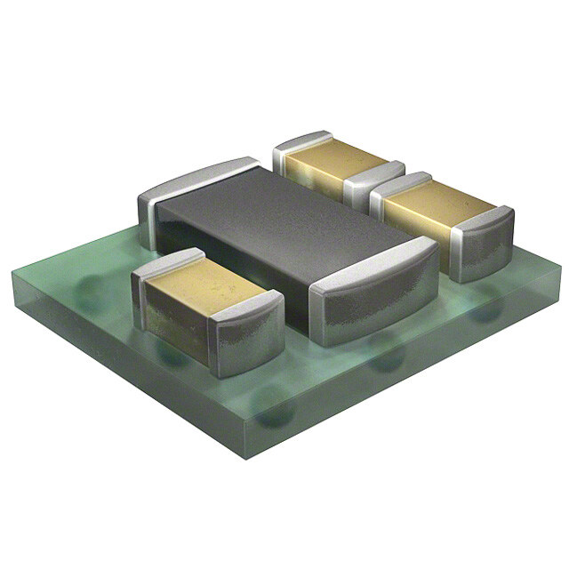
| 产品图片 |
|
| rohs | 符合RoHS含铅 / 不符合限制有害物质指令(RoHS)规范要求 |
| 产品系列 | 电源管理 IC,稳压器—开关式稳压器,Texas Instruments TPS82695SIPT- |
| 数据手册 | |
| 产品型号 | TPS82695SIPT |
| PWM类型 | 电压模式 |
| 产品种类 | 稳压器—开关式稳压器 |
| 供应商器件封装 | 8-uSIP (2.9x2.3) |
| 其它名称 | 296-32589-1 |
| 包装 | 剪切带 (CT) |
| 同步整流器 | 是 |
| 商标 | Texas Instruments |
| 安装类型 | 表面贴装 |
| 安装风格 | SMD/SMT |
| 封装 | Reel |
| 封装/外壳 | 8-SMD 模块 |
| 封装/箱体 | uSIP-8 |
| 工作温度 | -40°C ~ 85°C |
| 工作温度范围 | - 40 C to + 85 C |
| 工厂包装数量 | 250 |
| 开关频率 | 4 MHz |
| 拓扑结构 | Buck |
| 最大工作温度 | + 85 C |
| 最大输入电压 | 4.35 V |
| 最小工作温度 | - 40 C |
| 最小输入电压 | 2.3 V |
| 标准包装 | 1 |
| 电压-输入 | 2.3 V ~ 4.35 V |
| 电压-输出 | 2.5V |
| 电流-输出 | 500mA |
| 电源电压-最小 | 2.3 V |
| 类型 | Voltage Converter |
| 系列 | TPS82695 |
| 输入电压 | 2.3 V to 4.35 V |
| 输出数 | 1 |
| 输出电压 | 2.5 V |
| 输出电流 | 500 mA |
| 输出端数量 | 1 Output |
| 输出类型 | 固定 |
| 配用 | /product-detail/zh/TPS82695EVM-646/TPS82695EVM-646-ND/2833494 |
| 频率-开关 | 4MHz |


- 商务部:美国ITC正式对集成电路等产品启动337调查
- 曝三星4nm工艺存在良率问题 高通将骁龙8 Gen1或转产台积电
- 太阳诱电将投资9.5亿元在常州建新厂生产MLCC 预计2023年完工
- 英特尔发布欧洲新工厂建设计划 深化IDM 2.0 战略
- 台积电先进制程称霸业界 有大客户加持明年业绩稳了
- 达到5530亿美元!SIA预计今年全球半导体销售额将创下新高
- 英特尔拟将自动驾驶子公司Mobileye上市 估值或超500亿美元
- 三星加码芯片和SET,合并消费电子和移动部门,撤换高东真等 CEO
- 三星电子宣布重大人事变动 还合并消费电子和移动部门
- 海关总署:前11个月进口集成电路产品价值2.52万亿元 增长14.8%


PDF Datasheet 数据手册内容提取
TPS82690 TPS82695 TPS82697 www.ti.com SLVSA66B–JUNE2011–REVISEDFEBRUARY2012 500-mA, HIGH-EFFICIENCY MicroSiP™ STEP-DOWN CONVERTER (PROFILE <1mm) CheckforSamples:TPS82690,TPS82695,TPS82697 FEATURES 1 DESCRIPTION • TotalSolutionSize<6.7mm2 2 The TPS8269xSIP device is a complete 500mA, • 95%Efficiencyat4MHzOperation DC/DC step-down power supply intended for • 24μAQuiescentCurrent low-power applications. Included in the package are the switching regulator, inductor and input/output • HighDuty-CycleOperation capacitors. No additional components are required to • BestinClassLoadandLineTransient finishthedesign. • ±2%TotalDCVoltageAccuracy The TPS8269xSIP is based on a high-frequency • AutomaticPFM/PWMModeSwitching synchronous step-down dc-dc converter optimized for • LowRippleLight-LoadPFMMode battery-powered portable applications. The MicroSIP™ DC/DC converter operates at a regulated • ExcellentACLoadRegulation 4-MHz switching frequency and enters the • InternalSoftStart,130-µsStart-UpTime power-save mode operation at light load currents to • IntegratedActivePower-DownSequencing maintain high efficiency over the entire load current (Optional) range. • CurrentOverloadandThermalShutdown The PFM mode extends the battery life by reducing Protection the quiescent current to 24μA (typ) during light load • Sub1-mmProfileSolution operation. For noise-sensitive applications, the device has PWM spread spectrum capability providing a lower noise regulated output, as well as low noise at APPLICATIONS the input. These features, combined with high PSRR • LDOReplacement and AC load regulation performance, make this • CellPhones,Smart-Phones device suitable to replace a linear regulator to obtain betterpowerconversionefficiency. • PoLApplications The TPS8269xSIP is packaged in a compact (2.3mm x 2.9mm) and low profile (1.0mm) BGA package suitable for automated assembly by standard surface mountequipment. TPS82690SIP 100 150 V= 3.6 V, VBAT DVCI/NDC ConvertSeWr L VOUT 95 VIO= 2.85 V PFM/PEWffiMci eOnpceyration 135 3.25 V .. 4.35 V 2.85 V @ 500mA C C 90 120 I O GND FB 85 105 MODE W ENABLE FigureE1N. TyMGpNOiDDcEalApplication SELECTION Efficiency - % 778050 679050 ower Loss - m P 65 Power Loss 45 PFM/PWM Operation 60 30 55 15 50 0 0.1 1 10 100 1000 IO- Load Current - mA Figure2. Efficiencyvs.LoadCurrent 1 Pleasebeawarethatanimportantnoticeconcerningavailability,standardwarranty,anduseincriticalapplicationsofTexas Instrumentssemiconductorproductsanddisclaimerstheretoappearsattheendofthisdatasheet. MicroSiP,MicroSIParetrademarksofTexasInstruments. 2 UNLESS OTHERWISE NOTED this document contains Copyright©2011–2012,TexasInstrumentsIncorporated PRODUCTION DATA information current as of publication date. Products conform to specifications per the terms of Texas Instruments standard warranty. Production processing does not necessarilyincludetestingofallparameters.
TPS82690 TPS82695 TPS82697 SLVSA66B–JUNE2011–REVISEDFEBRUARY2012 www.ti.com Thesedeviceshavelimitedbuilt-inESDprotection.Theleadsshouldbeshortedtogetherorthedeviceplacedinconductivefoam duringstorageorhandlingtopreventelectrostaticdamagetotheMOSgates. ORDERINGINFORMATION(1) TA NUPMARBTER VOOLUTTAPGUET(2) SPECIDFIECVFICEEATURE ORDERING(3) PMAACRKKAINGGE TPS82695 2.5V TPS82695SIP UF TPS82690(4) 2.85V TPS82690SIP RC -40°Cto85°C TPS82696(4) 2.9V TPS82696SIP TPS82697(4) 2.8V TPS82697SIP (1) Forthemostcurrentpackageandorderinginformation,seethePackageOptionAddendumattheendofthisdocument,orseetheTI websiteatwww.ti.com. (2) Internaltappointsareavailabletofacilitateoutputvoltagesin25mVincrements. (3) TheSIPpackageisavailableintapeandreel.AddaRsuffix(e.g.TPS82690SIPR)toorderquantitiesof3000parts.AddaTsuffix(e.g. TPS82690SIPT)toorderquantitiesof250parts. (4) Productpreview.ContactTIfactoryformoreinformation ABSOLUTE MAXIMUM RATINGS overoperatingfree-airtemperaturerange(unlessotherwisenoted)(1) UNIT VoltageatVIN(2)(3) –0.3Vto6V V VoltageatVOUT(3) –0.3Vto3.6V I VoltageatEN,MODE (3) –0.3VtoV +0.3V I I Peakoutputcurrent 500mA O Powerdissipation Internallylimited T Operatingtemperaturerange(4) –40°Cto85°C A T (max) Maximuminternaloperatingtemperature 125°C INT T Storagetemperaturerange –55°Cto125°C stg Humanbodymodel 2kV ESDrating (5) Chargedevicemodel 1kV Machinemodel 200V (1) Stressesbeyondthoselistedunderabsolutemaximumratingsmaycausepermanentdamagetothedevice.Thesearestressratings onlyandfunctionaloperationofthedeviceattheseoranyotherconditionsbeyondthoseindicatedunderrecommendedoperating conditionsisnotimplied.Exposuretoabsolute-maximum-ratedconditionsforextendedperiodsmayaffectdevicereliability. (2) Operationabove4.35Vinputvoltageforextendedperiodsmayaffectdevicereliability.Seeinputcapacitorselectionsectionformore details. (3) Allvoltagevaluesarewithrespecttonetworkgroundterminal. (4) Inapplicationswherehighpowerdissipationand/orpoorpackagethermalresistanceispresent,themaximumambienttemperaturemay havetobederated.Maximumambienttemperature(T )isdependentonthemaximumoperatingtemperature(T ),the A(max) INT(max) maximumpowerdissipationofthedeviceintheapplication(P ),andthejunction-to-ambientthermalresistanceofthepart/package D(max) intheapplication(θ ),asgivenbythefollowingequation:T =T –(θ XP ).Toachieveoptimumperformance,itis JA A(max) J(max) JA D(max) recommendedtooperatethedevicewithamaximuminternaltemperatureof105°C. (5) Thehumanbodymodelisa100-pFcapacitordischargedthrougha1.5-kΩresistorintoeachpin.Themachinemodelisa200-pF capacitordischargeddirectlyintoeachpin. 2 Copyright©2011–2012,TexasInstrumentsIncorporated
TPS82690 TPS82695 TPS82697 www.ti.com SLVSA66B–JUNE2011–REVISEDFEBRUARY2012 THERMAL INFORMATION TPS82690/95/97 THERMALMETRIC(1) UNITS SIP(8-Pins) Junction-to-ambient(top)thermalresistance 125 θ JA Junction-to-ambient(bottom)thermalresistance 70 θ Junction-to-case(top)thermalresistance – JCtop θ Junction-to-boardthermalresistance – °C/W JB ψ Junction-to-topcharacterizationparameter – JT ψ Junction-to-boardcharacterizationparameter – JB θ Junction-to-case(bottom)thermalresistance – JCbot (1) Formoreinformationabouttraditionalandnewthermalmetrics,seetheICPackageThermalMetricsapplicationreport,SPRA953. RECOMMENDED OPERATING CONDITIONS MIN NOM MAX UNIT V Inputvoltagerange 2.3 4.35(1) V I I Outputcurrentrange 0 500 mA O Additionaloutputcapacitance(PFM/PWMoperation)(2) 0 5 µF Additionaloutputcapacitance(PWMoperation)(2) 0 8 µF T Ambienttemperature –40 +85 °C A T Operatingjunctiontemperature –40 +125 °C J (1) Operationabove4.35Vinputvoltageforextendedperiodsmayaffectdevicereliability.Seeinputcapacitorselectionsectionformore details. (2) Incertainapplicationslargercapacitorvaluescanbetolerable,seeoutputcapacitorselectionsectionformoredetails. ELECTRICAL CHARACTERISTICS MinimumandmaximumvaluesareatV =2.3Vto4.35V,V =2.5V,EN=1.8V,AUTOmodeandT =–40°Cto85°C;Circuit I O A ofParameterMeasurementInformationsection(unlessotherwisenoted).TypicalvaluesareatV =3.6V,V =2.5V,EN= I O 1.8V,AUTOmodeandT =25°C(unlessotherwisenoted). A PARAMETER TESTCONDITIONS MIN TYP MAX UNIT SUPPLYCURRENT Operatingquiescent IO=0mA.Devicenotswitching 24 50 μA IQ current TPS82690 IO=0mA,PWMmode 4.5 mA ISD Shutdowncurrent TPS8269X EN=GND 0.5 5 μA TPS82690 Undervoltage TPS82695 2.05 2.1 V UVLO lockoutthreshold TPS82697 TPS82696 2.1 2.15 V PROTECTION Thermalshutdown 140 °C Thermalshutdown TPS8269X 10 °C hysteresis Peakinputcurrent ILIM limit TPS8269X 750 mA Inputcurrentlimit ISC undershort-circuit TPS8269X VOshortedtoground 15 mA conditions ENABLE,MODE High-levelinput VIH voltage 1.0 V Low-levelinput VIL voltage TPS8269X 0.4 V Inputleakage InputconnectedtoGNDorVIN 0.01 1.5 μA current OSCILLATOR fSW Oscillatorfrequency TPS8269X IO=0mA.PWMoperation.TA=25°C 3.6 4 4.4 MHz Copyright©2011–2012,TexasInstrumentsIncorporated SubmitDocumentationFeedback 3 ProductFolderLink(s):TPS82690TPS82695TPS82697
TPS82690 TPS82695 TPS82697 SLVSA66B–JUNE2011–REVISEDFEBRUARY2012 www.ti.com ELECTRICAL CHARACTERISTICS (continued) MinimumandmaximumvaluesareatV =2.3Vto4.35V,V =2.5V,EN=1.8V,AUTOmodeandT =–40°Cto85°C;Circuit I O A ofParameterMeasurementInformationsection(unlessotherwisenoted).TypicalvaluesareatV =3.6V,V =2.5V,EN= I O 1.8V,AUTOmodeandT =25°C(unlessotherwisenoted). A PARAMETER TESTCONDITIONS MIN TYP MAX UNIT OUTPUT 3P.F2M5V/P≤WVMI≤op4e.3r5aVtio,n0mA≤IO≤500mA 0.98×VNOM VNOM 1.04×VNOM V 3.25V≤VI≤4.35V,0mA≤IO≤500mA TPS82690 A(mdudRitiaotnaaGloRuMtp1u5t5cRap6a0cJi4to7r5,MC)O=4.7μF6.3V0402 0.98×VNOM VNOM 1.03×VNOM V TPS82697 PFM/PWMoperation 3P.F2M5V/P≤WVMI≤op5e.5rVat,io0nmA≤IO≤500mA 0.98×VNOM VNOM 1.05×VNOM V 3P.W25MVo≤pVerIa≤ti5o.n5V,0mA≤IO≤500mA 0.98×VNOM VNOM 1.02×VNOM V RegulatedDC 3P.F0MV/≤PWVIM≤o4p.3e5rVat,io0nmA≤IO≤500mA 0.98×VNOM VNOM 1.04×VNOM V V(OUT) outputvoltage TPS82695 3P.F0MV/≤PWVIM≤o5p.5eVra,t0iomnA≤IO≤500mA 0.97×VNOM VNOM 1.05×VNOM V 3P.W0VM≤oVpeI≤ra5ti.o5nV,0mA≤IO≤500mA 0.98×VNOM VNOM 1.02×VNOM V 3P.F2M5V/P≤WVMI≤op5e.5rVat,io0nmA≤IO≤500mA 0.97×VNOM VNOM 1.05×VNOM V 3.25V≤VI≤4.35V,0mA≤IO≤500mA TPS82696 A(mdudRitiaotnaaGloRuMtp1u5t5cRap6a0cJi4to7r5,MC)O=4.7μF6.3V0402 0.97×VNOM VNOM 1.04×VNOM V PFM/PWMoperation 3P.W25MVo≤pVerIa≤ti5o.n5V,0mA≤IO≤500mA 0.97×VNOM VNOM 1.03×VNOM V Lineregulation VI=VO+0.5V(min3.25V)to5.5V,IO=200mA 0.18 %/V TPS8269X Loadregulation IO=0mAto500mA.PWMoperation –0.0002 %/mA Feedbackinput TPS8269X 480 kΩ resistance Input-to-output rDS(on) On-resistance TPS8269X VI=3.25V.Devicenotswitching 390 mΩ IO=1mA 70 mVPP ΔVO Pripopwleerv-soaltvaegemode TPS8269X IAOd=di1tiomnAaloutputcapacitor,CO=4.7μF6.3V0402 35 mVPP (muRataGRM155R60J475M) TPS82690 IO=0mA,TimefromactiveENtoVO 130 μs Start-uptime TPS82696 TimefromactiveENtofullloadcurrentoperation TPS82697 permitted 350 μs Dischargeresistor rDIS forpower-down TPS8269X 100 150 Ω sequence 4 SubmitDocumentationFeedback Copyright©2011–2012,TexasInstrumentsIncorporated ProductFolderLink(s):TPS82690TPS82695TPS82697
TPS82690 TPS82695 TPS82697 www.ti.com SLVSA66B–JUNE2011–REVISEDFEBRUARY2012 PIN ASSIGNMENTS SIP-8 SIP-8 (TOPVIEW) (BOTTOM VIEW) VOUT A1 A2 A3 VIN VIN A3 A2 A1 VOUT MODE B1 B2 EN EN B2 B1 MODE GND C1 C2 C3 GND GND C3 C2 C1 GND TERMINALFUNCTIONS TERMINAL I/O DESCRIPTION NAME NO. VOUT A1 O Poweroutputpin.ApplyoutputloadbetweenthispinandGND. VIN A2,A3 I TheVINpinssupplycurrenttotheTPS8269xSIP'sinternalregulator. Thisistheenablepinofthedevice.Connectingthispintogroundforcestheconverterinto EN B2 I shutdownmode.PullingthispintoV enablesthedevice.Thispinmustnotbeleftfloatingand I mustbeterminated. Thisisthemodeselectionpinofthedevice.Thispinmustnotbeleftfloatingandmustbe terminated. MODE=LOW:Thedeviceisoperatinginregulatedfrequencypulsewidthmodulationmode MODE B1 I (PWM)athigh-loadcurrentsandinpulsefrequencymodulationmode(PFM)atlightload currents. MODE=HIGH:Low-noisemodeenabled,regulatedfrequencyPWMoperationforced. GND C1,C2,C3 – Groundpin. FUNCTIONAL BLOCK DIAGRAM MODE EN VIN C I 4.7µF DC/DC CONVERTER Undervoltage VIN Lockout Bias Supply Soft-Start Negative Inductor Current Detect Bandgap VREF=0.8V Power Save Mode Switching Thermal Current Limit Shutdown Detect Frequency Control R1 - L Gate Driver VOUT R2 VREF ShootA-Tnhtirough 1µH C O + 4.7µF Feedback Divider GND Copyright©2011–2012,TexasInstrumentsIncorporated SubmitDocumentationFeedback 5 ProductFolderLink(s):TPS82690TPS82695TPS82697
TPS82690 TPS82695 TPS82697 SLVSA66B–JUNE2011–REVISEDFEBRUARY2012 www.ti.com PARAMETER MEASUREMENT INFORMATION TPS8269XSIP DC/DC Converter L VBAT VIN SW VOUT C C I O GND FB MODE ENABLE EN MODE SELECTION GND TYPICAL CHARACTERISTICS Table of Graphs FIGURE vsLoadcurrent 3,4 η Efficiency vsLoadcurrent 5,6 vsInputvoltage 7 Peak-to-peakoutputripplevoltage vsLoadcurrent 8,9 V DCoutputvoltage vsLoadcurrent 10,11,120 O Combinedline/loadtransient 13,14 response Loadtransientresponse 15,16,17,18 ACloadtransientresponse 19,20,21,22,23,24,25 PFM/PWMboundaries vsInputvoltage 26 I Quiescentcurrent vsInputvoltage 27 Q PWMswitchingfrequency vsInputvoltage 28 f s PFMswitchingfrequency vsLoadcurrent 29 Start-up 30,31 PSRR Powersupplyrejectionratio vs.Frequency 32 6 SubmitDocumentationFeedback Copyright©2011–2012,TexasInstrumentsIncorporated ProductFolderLink(s):TPS82690TPS82695TPS82697
TPS82690 TPS82695 TPS82697 www.ti.com SLVSA66B–JUNE2011–REVISEDFEBRUARY2012 TYPICAL CHARACTERISTICS (continued) TPS82695 TPS82695 EFFICIENCY EFFICIENCY vs vs LOADCURRENT LOADCURRENT 100 100 VI= 3 V VO= 2.5 V 90 90 Forced PWM 80 80 V = 3.2 V I 70 70 V = 3 V I % V = 3.6 V % 60 I 60 y - y - c c en 50 VI= 4.2 V en 50 VI= 3.2 V ci ci Effi 40 Effi 40 30 30 V = 3.6 V V = 3.6 V I I 20 Forced PWM Operation 20 V = 4.2 V I 10 10 V = 2.5 V O 0 0 0.1 1 10 100 1000 1 10 100 1000 I - Load Current - mA I - Load Current - mA O O Figure3. Figure4. EFFICIENCY EFFICIENCY vs vs LOADCURRENT LOADCURRENT 100 100 VO= 2.85 V VO= 2.85 V 90 90 V = 3 V I V = 3 V 80 VI= 3.2 V I 80 Forced PWM V = 3.2 V 70 V = 3.6 V 70 I I Forced PWM % 60 V = 4.2 V % 60 ncy - 50 I ncy - 50 VI= 3.6 V e e Forced PWM ci ci Effi 40 Effi 40 V = 4.2 V I 30 30 Forced PWM V = 3.6 V I 20 Forced PWM Operation 20 10 10 0 0 0.1 1 10 100 1000 1 10 100 1000 IO- Load Current - mA IO- Load Current - mA Figure5. Figure6. Copyright©2011–2012,TexasInstrumentsIncorporated SubmitDocumentationFeedback 7 ProductFolderLink(s):TPS82690TPS82695TPS82697
TPS82690 TPS82695 TPS82697 SLVSA66B–JUNE2011–REVISEDFEBRUARY2012 www.ti.com TYPICAL CHARACTERISTICS (continued) EFFICIENCY PEAK-TO-PEAKOUTPUTRIPPLEVOLTAGE vs vs INPUTVOLTAGE LOADCURRENT 100 100 V = 2.85 V V = 2.85 V O O V 98 PFM/PWM Operation m 90 e - g 80 96 a IO= 100 mA IO= 300 mA Volt 70 VI= 3.3 V 94 e pl cy - % 92 ut Rip 60 n p 50 Efficie 90 IO= 1 mA ak Out 40 VI= 4.5 V 88 IO= 10 mA o-Pe 30 VI= 3.6 V 86 k-t ea 20 P 84 - O 10 V PFM/PWM Operation 82 0 2.9 3.1 3.3 3.5 3.7 3.9 4.1 4.3 4.5 4.7 4.9 0 50 100 150 200 250 300 350 400 450 500 VI- Input Voltage - V IO- Load Current - mA Figure7. Figure8. PEAK-TO-PEAKOUTPUTRIPPLEVOLTAGE DCOUTPUTVOLTAGE vs vs LOADCURRENT LOADCURRENT 55 2.936 V = 2.85 V V = 2.85 V O O mV 50 CO(additional) = 4.7mF 0402 6.3 V X5R PFM/PWM Operation V = 3.2 V age - 45 VI= 3.3 V 2.907 I olt 40 V V utput Ripple 233505 VI= 4.5 V put Voltage - 2.28.7895 VI= 4.5 V VI= 3.6 V k O Out ea 20 - 2.822 P V = 3.6 V O o- 15 I V k-t VI= 3 V a Pe 10 2.793 - O 5 V PFM/PWM Operation 0 2.765 0 50 100 150 200 250 300 350 400 450 500 0.1 1 10 100 1000 I - Load Current - mA I - Load Current - mA O O Figure9. Figure10. 8 SubmitDocumentationFeedback Copyright©2011–2012,TexasInstrumentsIncorporated ProductFolderLink(s):TPS82690TPS82695TPS82697
TPS82690 TPS82695 TPS82697 www.ti.com SLVSA66B–JUNE2011–REVISEDFEBRUARY2012 TYPICAL CHARACTERISTICS (continued) DCOUTPUTVOLTAGE DCOUTPUTVOLTAGE vs vs LOADCURRENT LOADCURRENT 2.936 2.907 V = 3 V, T = 85°C VI= 3 V, TA= 25°C VI= 3 V V = 3.2 V I A I V = 4.5 V 2.907 I 2.879 Output Voltage - V 22..288.278295 VI= 3.2 V, TA=V 2I5=° C3.1 V, TA= 85°C Output Voltage - V 2.28.2825 VI= 3.6 V V- O 2.793 VI= 3.2 V, TA= 85°C V- O V = 2.85 V 2.793 O C (additional) = 4.7mF 0402 3.6 V X5R 2.765 V = 2.85 V O O PFM/PWM Operation PFM/PWM Operation 2.736 2.765 0.1 1 10 100 1000 0.1 1 10 100 1000 IO- Load Current - mA IO- Load Current - mA Figure11. Figure12. COMBINEDLINE/LOADTRANSIENTRESPONSE COMBINEDLINE/LOADTRANSIENTRESPONSE VO= 2.85 V MODE = Low VO= 2.85 V MODE = Low 10 to 400 mALoad Step 10 to 400 mALoad Step 3.3V to 3.9V mALine Step 3.15V to 3.75V mALine Step Figure13. Figure14. Copyright©2011–2012,TexasInstrumentsIncorporated SubmitDocumentationFeedback 9 ProductFolderLink(s):TPS82690TPS82695TPS82697
TPS82690 TPS82695 TPS82697 SLVSA66B–JUNE2011–REVISEDFEBRUARY2012 www.ti.com TYPICAL CHARACTERISTICS (continued) LOADTRANSIENTRESPONSEIN LOADTRANSIENTRESPONSEIN PFM/PWMOPERATION PFM/PWMOPERATION VI= 3.6 V, 10 to 400 mALoad Step VO= 2.85 V 5 to 250 mALoad Step VI= 3.6 V, MODE = Low VO= 2.85 V MODE = Low Figure15. Figure16. LOADTRANSIENTRESPONSEIN LOADTRANSIENTRESPONSEIN PFM/PWMOPERATION PFM/PWMOPERATION 10 to 400 mALoad Step 10 to 400 mALoad Step VI= 3.25 V, VI= 4.8 V, VO= 2.85 V MODE = Low VO= 2.85 V MODE = Low Figure17. Figure18. 10 SubmitDocumentationFeedback Copyright©2011–2012,TexasInstrumentsIncorporated ProductFolderLink(s):TPS82690TPS82695TPS82697
TPS82690 TPS82695 TPS82697 www.ti.com SLVSA66B–JUNE2011–REVISEDFEBRUARY2012 TYPICAL CHARACTERISTICS (continued) ACLOADTRANSIENTRESPONSE ACLOADTRANSIENTRESPONSE VI = 3.6 V, VI = 3.0 V, VO= 2.5 V VO= 2.5 V 5 to 500 mALoad Sweep 5 to 500 mALoad Sweep MODE = Low MODE = Low Figure19. Figure20. ACLOADTRANSIENTRESPONSE ACLOADTRANSIENTRESPONSE VI = 2.85 V, VI= 3.05 V, VO= 2.5 V VO= 2.85 V 5 to 600 mALoad Sweep 5 to 600 mALoad Sweep MODE = Low MODE = Low Figure21. Figure22. Copyright©2011–2012,TexasInstrumentsIncorporated SubmitDocumentationFeedback 11 ProductFolderLink(s):TPS82690TPS82695TPS82697
TPS82690 TPS82695 TPS82697 SLVSA66B–JUNE2011–REVISEDFEBRUARY2012 www.ti.com TYPICAL CHARACTERISTICS (continued) ACLOADTRANSIENTRESPONSE ACLOADTRANSIENTRESPONSE VI= 3.15 V, VI= 3.6 V, VO= 2.85 V VO= 2.85 V 5 to 500 mALoad Sweep 5 to 500 mALoad Sweep MODE = Low MODE = Low Figure23. Figure24. ACLOADTRANSIENTRESPONSE PFM/PWMBOUNDARIES 280 V = 2.85 V VI= 3.6 V, 260 O VO= 2.85 V 240 Always PWM 220 5 to 500 mALoad Sweep PFM to PWM 200 Mode Change A m 180 nt - 160 The switching mode changes e at these borders r ur 140 C d 120 a o Always PFM L 100 PWM to PFM - O 80 Mode Change I CO= add. 4.7µF 6.3V X5R 0402 MODE = Low 60 40 20 0 3.2 3.4 3.6 3.8 4.0 4.2 4.4 4.6 4.8 V - Input Voltage - V I Figure25. Figure26. 12 SubmitDocumentationFeedback Copyright©2011–2012,TexasInstrumentsIncorporated ProductFolderLink(s):TPS82690TPS82695TPS82697
TPS82690 TPS82695 TPS82697 www.ti.com SLVSA66B–JUNE2011–REVISEDFEBRUARY2012 TYPICAL CHARACTERISTICS (continued) QUIESCENTCURRENT PWMSWITCHINGFREQUENCY vs vs INPUTVOLTAGE INPUTVOLTAGE 38 4.2 36 TA= 85°C 4 34 32 T = 25°C 3.8 A 30 Am 28 MHz 3.6 nt - 2246 cy - 3.4 urre 22 uen 3.2 IO= 500 mA C 20 q 3 nt 18 Fre IO= 300 mA ce 16 g 2.8 uies 14 TA= -40°C chin 2.6 IO= 150 mA I- QQ 11028 - Swits 22..24 IO= 50 mA 6 f 4 2 V = 2.85 V 2 1.8 O 0 MODE = High 2.7 3 3.3 3.6 3.9 4.2 4.5 4.8 1.6 V - Input Voltage - V 2.9 3.1 3.3 3.5 3.7 3.9 4.1 4.3 4.5 I V - Input Voltage - V I Figure27. Figure28. PFMSWITCHINGFREQUENCY vs LOADCURRENT START-UP 4.5 VO= 2.85 V VI= 4.5 V 4 MODE = Low z 3.5 H M cy - 3 VVIO== 3 2.6.8 V5, V, uen 2.5 VI= 3.6 V IO= 0 mA q e r F g 2 n hi c wit 1.5 V = 3.2 V S I - s 1 MODE = Low f 0.5 0 0 40 80 120 160 200 240 280 320 360 400 I - Load Current - mA O Figure29. Figure30. Copyright©2011–2012,TexasInstrumentsIncorporated SubmitDocumentationFeedback 13 ProductFolderLink(s):TPS82690TPS82695TPS82697
TPS82690 TPS82695 TPS82697 SLVSA66B–JUNE2011–REVISEDFEBRUARY2012 www.ti.com TYPICAL CHARACTERISTICS (continued) POWERSUPPLYREJECTIONRATIO vs START-UP FREQUENCY 60 I = 20 mA O 55 PWM Operation B d o - 50 ati 45 R VVRIOL=== 3 32.69.8 VW5, V, ejection 3450 IPOW=M 2 5O0p merAation R I = 400 mA y 30 O pl PWM Operation p 25 u S er 20 w o P 15 MODE = Low R - 10 IO= 20 mA R PFM Operation S P 5 0 0.1 1 10 100 1000 f - Frequency - kHz Figure31. Figure32. 14 SubmitDocumentationFeedback Copyright©2011–2012,TexasInstrumentsIncorporated ProductFolderLink(s):TPS82690TPS82695TPS82697
TPS82690 TPS82695 TPS82697 www.ti.com SLVSA66B–JUNE2011–REVISEDFEBRUARY2012 DETAILED DESCRIPTION OPERATION The TPS8269xSIP is a standalone synchronous step-down converter operating at a regulated 4-MHz frequency pulse width modulation (PWM) at moderate to heavy load currents (up to 500mA output current). At light load currents,theTPS8269xSIP'sconverteroperatesinpower-savemodewithpulsefrequencymodulation(PFM). The converter uses a unique frequency locked ring oscillating modulator to achieve best-in-class load and line response. One key advantage of the non-linear architecture is that there is no traditional feed-back loop. The loop response to change in V is essentially instantaneous, which explains the transient response. Although this O type of operation normally results in a switching frequency that varies with input voltage and load current, an internal frequency lock loop (FLL) holds the switching frequency constant over a large range of operating conditions. Combined with best in class load and line transient response characteristics, the low quiescent current of the device (ca. 24μA) allows to maintain high efficiency at light load, while preserving fast transient response for applicationsrequiringtightoutputregulation. The TPS8269xSIP integrates an input current limit to protect the device against heavy load or short circuits and featuresanundervoltagelockoutcircuittopreventthedevicefrommisoperationatlowinputvoltages. POWER-SAVE MODE If the load current decreases, the converter will enter Power Save Mode operation automatically. During power-save mode the converter operates in discontinuous current (DCM) with a minimum of one pulse, which produceslowoutputripplecomparedwithotherPFMarchitectures. When in power-save mode, the converter resumes its operation when the output voltage trips below the nominal voltage. It ramps up the output voltage with a minimum of one pulse and goes into power-save mode when the outputvoltageiswithinitsregulationlimitsagain. PFM mode is left and PWM operation is entered as the output current can no longer be supported in PFM mode. As a consequence, the DC output voltage is typically positioned ca. 1.5% above the nominal output voltage and thetransitionbetweenPFMandPWMisseamless. PFM Mode at Light Load PFM Ripple Nominal DC Output Voltage PWM Mode at Heavy Load Figure33. OperationinPFMModeandTransfertoPWMMode Copyright©2011–2012,TexasInstrumentsIncorporated SubmitDocumentationFeedback 15 ProductFolderLink(s):TPS82690TPS82695TPS82697
TPS82690 TPS82695 TPS82697 SLVSA66B–JUNE2011–REVISEDFEBRUARY2012 www.ti.com MODE SELECTION The MODE pin allows to select the operating mode of the device. Connecting this pin to GND enables the automatic PWM and power-save mode operation. The converter operates in regulated frequency PWM mode at moderate to heavy loads and in the PFM mode during light loads, which maintains high efficiency over a wide loadcurrentrange. Pulling the MODE pin high forces the converter to operate in the PWM mode even at light load currents. The advantage is that the converter operates with a fixed frequency that allows simple filtering of the switching frequency for noise-sensitive applications. In this mode, the efficiency is lower compared to the power-save modeduringlightloads. For additional flexibility, it is possible to switch from power-save mode to PWM mode during operation. This allows efficient power management by adjusting the operation of the converter to the specific system requirements. LOW DROPOUT, 100% DUTY CYCLE OPERATION The device starts to enter 100% duty cycle mode once input and output voltage come close together. In order to maintain the output voltage, the DC/DC converter's high-side MOSFET is turned on 100% for one or more cycles. With further decreasing V the high-side switch is constantly turned on, thereby providing a low input-to-output IN voltage difference. This is particularly useful in battery-powered applications to achieve longest operation time by takingfulladvantageofthewholebatteryvoltagerange. SOFT START The TPS8269xSIP has an internal soft-start circuit that limits the inrush current during start-up. This limits input voltage drops when a battery or a high-impedance power source is connected to the input of the MicroSiP™ converter. The soft-start system progressively increases the switching on-time from a minimum pulse-width of 35ns as a function of the output voltage. This mode of operation continues for c.a. 100μs after enable. Should the output voltage not have reached its target value by that time, such as in the case of heavy load, the soft-start transitions toasecondmodeofoperation. If the output voltage has raised above 0.5V (approximately), the converter increases the input current limit thereby enabling the power supply to come-up properly. The start-up time mainly depends on the capacitance presentattheoutputnodeandloadcurrent. ENABLE The TPS8269xSIP device starts operation when EN is set high and starts up with the soft start as previously described.Forproperoperation,theENpinmustbeterminatedandmustnotbeleftfloating. Pulling the EN pin low forces the device into shutdown. In this mode, all internal circuits are turned off and V IN currentreducestothedeviceleakagecurrent,typicallyafewhundrednanoamps. The TPS8269xSIP device can actively discharge the output capacitor when it turns off (refer to Ordering Information Table). The integrated discharge resistor has a typical resistance of 100 Ω. The required time to ramp-downtheoutputvoltagedependsontheloadcurrentandthecapacitancepresentattheoutputnode. 16 SubmitDocumentationFeedback Copyright©2011–2012,TexasInstrumentsIncorporated ProductFolderLink(s):TPS82690TPS82695TPS82697
TPS82690 TPS82695 TPS82697 www.ti.com SLVSA66B–JUNE2011–REVISEDFEBRUARY2012 APPLICATION INFORMATION INPUT CAPACITOR SELECTION Because of the pulsating input current nature of the buck converter, a low ESR input capacitor is required to prevent large voltage transients that can cause misbehavior of the device or interference in other circuits in the system. For most applications, the input capacitor that is integrated into the TPS8269x should be sufficient. If the application exhibits a noisy or erratic switching frequency, experiment with additional input ceramic capacitance tofindaremedy. The TPS8269x uses a tiny ceramic input capacitor. When a ceramic capacitor is combined with trace or cable inductance, such as from a wall adapter, a load step at the output can induce ringing at the VIN pin. This ringing can couple to the output and be mistaken as loop instability or can even damage the part. In this circumstance, additional "bulk" capacitance, such as electrolytic or tantalum, should be placed between the input of the converter and the power source lead to reduce ringing that can occur between the inductance of the power sourceleadsandC. I OUTPUT CAPACITOR SELECTION The advanced, fast-response, voltage mode, control scheme of the TPS8269x allows the use of a tiny ceramic outputcapacitor(C ).Formostapplications,theoutputcapacitorintegratedintheTPS8269xissufficient. O At nominal load current, the device operates in PWM mode; the overall output voltage ripple is the sum of the voltage step that is caused by the output capacitor ESL and the ripple current that flows through the output capacitor impedance. At light loads, the output capacitor limits the output ripple voltage and provides holdup duringlargeloadtransitions. The TPS8269x is designed as a Point-Of-Load (POL) regulator, to operate stand-alone without requiring any additional capacitance. Adding a 4.7μF ceramic output capacitor (X7R or X5R dielectric) generally works from a converter stability point of view, helps to minimize the output ripple voltage in PFM mode and improves the converter'stransientresponseunderwheninputandoutputvoltageareclosetogether. For best operation (i.e. optimum efficiency over the entire load current range, proper PFM/PWM auto transition), the TPS8269xSIP requires a minimum output ripple voltage in PFM mode. The typical output voltage ripple is ca. 1% of the nominal output voltage V . The PFM pulses are time controlled resulting in a PFM output voltage O ripple and PFM frequency that depends (first order) on the capacitance seen at the MicroSiPTM DC/DC converter'soutput. In applications requiring additional output bypass capacitors located close to the load, care should be taken to ensure proper operation. If the converter exhibits marginal stability or erratic switching frequency, experiment withadditionallowvalueseriesresistance(e.g.50to100mΩ)intheoutputpathtofindaremedy. Because the damping factor in the output path is directly related to several resistive parameters (e.g. inductor DCR, power-stage r , PWB DC resistance, load switches r …) that are temperature dependant, the DS(on) DS(on) converter small and large signal behavior must be checked over the input voltage range, load current range and temperaturerange. Theeasiestsanitytestistoevaluate,directlyattheconverter’soutput,thefollowingaspects: • PFM/PWMefficiency • PFM/PWMandforcedPWMloadtransientresponse Duringtherecoverytimefromaloadtransient,theoutputvoltagecanbemonitoredforsettlingtime,overshootor ringingthathelpsjudgetheconverter’sstability.Withoutanyringing,theloophasusuallymorethan45° ofphase margin. Copyright©2011–2012,TexasInstrumentsIncorporated SubmitDocumentationFeedback 17 ProductFolderLink(s):TPS82690TPS82695TPS82697
TPS82690 TPS82695 TPS82697 SLVSA66B–JUNE2011–REVISEDFEBRUARY2012 www.ti.com LAYOUT CONSIDERATION In making the pad size for the SiP LGA balls, it is recommended that the layout use non-solder-mask defined (NSMD) land. With this method, the solder mask opening is made larger than the desired land area, and the opening size is defined by the copper pad width. Figure 34 shows the appropriate diameters for a MicroSiPTM layout. Figure34. RecommendedLandPatternImageandDimensions SOLDERPAD SOLDERMASK (5) COPPER STENCIL (6) DEFINITIONS(1)(2)(3)(4) COPPERPAD OPENING THICKNESS OPENING STENCILTHICKNESS Non-solder-mask 0.30mm 0.360mm 1ozmax(0.032mm) 0.34mmdiameter 0.1mmthick defined(NSMD) (1) Circuittracesfromnon-solder-maskdefinedPWBlandsshouldbe75μmto100μmwideintheexposedareainsidethesoldermask opening.Widertracewidthsreducedevicestandoffandaffectreliability. (2) BestreliabilityresultsareachievedwhenthePWBlaminateglasstransitiontemperatureisabovetheoperatingtherangeofthe intendedapplication. (3) RecommendsolderpasteisType3orType4. (4) ForaPWBusingaNi/Ausurfacefinish,thegoldthicknessshouldbelessthan0.5mmtoavoidareductioninthermalfatigue performance. (5) Soldermaskthicknessshouldbelessthan20μmontopofthecoppercircuitpattern. (6) Forbestsolderstencilperformanceuselasercutstencilswithelectropolishing.Chemicallyetchedstencilsgiveinferiorsolderpaste volumecontrol. SURFACE MOUNT INFORMATION The TPS8269x MicroSiP™ DC/DC converter uses an open frame construction that is designed for a fully automated assembly process and that features a large surface area for pick and place operations. See the "Pick Area"inthepackagedrawings. Package height and weight have been kept to a minimum thereby to allow the MicroSiP™ device to be handled similarlytoa0805component. SeeJEDEC/IPCstandardJ-STD-20bforreflowrecommendations. 18 SubmitDocumentationFeedback Copyright©2011–2012,TexasInstrumentsIncorporated ProductFolderLink(s):TPS82690TPS82695TPS82697
TPS82690 TPS82695 TPS82697 www.ti.com SLVSA66B–JUNE2011–REVISEDFEBRUARY2012 THERMAL INFORMATION ThedietemperatureoftheTPS8269xmustbelowerthanthemaximumratingof125°C,socareshouldbetaken inthelayoutofthecircuittoensuregoodheatsinkingoftheTPS8269x. To estimate the junction temperature, approximate the power dissipation within the TPS8269x by applying the typical efficiency stated in this datasheet to the desired output power; or, by taking a power measurement if you haveanactualTPS8269xdeviceandTPS8269xEVMevaluationmodule.Thencalculatetheinternaltemperature rise of the TPS8269x above the surface of the printed circuit board by multiplying the TPS8269x power dissipationbythethermalresistance. The actual thermal resistance of the TPS8269x to the printed circuit board depends on the layout of the circuit board,butthethermalresistancegivenintheThermalInformationTablecanbeusedasaguide. Threebasicapproachesforenhancingthermalperformancearelistedbelow: • ImprovethepowerdissipationcapabilityofthePCBdesign. • ImprovethethermalcouplingofthecomponenttothePCB. • Introduceairflowintothesystem. PACKAGE SUMMARY SIPPACKAGE TOPVIEW BOTTOM VIEW A1 YML C1 C2 C3 D B1 B2 CC LSB A1 A2 A3 E Code: • CC—CustomerCode(device/voltagespecific) • YML—Y:Year,M:Month,L:Lottracecode • LSB—L:Lottracecode,S:Sitecode,B:Boardlocator MicroSiPTM DC/DC MODULE PACKAGE DIMENSIONS TheTPS8269xdeviceisavailableinan8-bumpballgridarray(BGA)package.Thepackagedimensionsare: • D=2.30±0.05mm • E=2.90±0.05mm Copyright©2011–2012,TexasInstrumentsIncorporated SubmitDocumentationFeedback 19 ProductFolderLink(s):TPS82690TPS82695TPS82697
TPS82690 TPS82695 TPS82697 SLVSA66B–JUNE2011–REVISEDFEBRUARY2012 www.ti.com Note:Pagenumbersofcurrentversionmaydifferfrompreviousversions. ChangesfromOriginal(June2011)toRevisionA Page • DeletedProductPreviewstatusfromTPS82695deviceinOrderingInformationtable. ...................................................... 2 ChangesfromRevisionA(October2011)toRevisionB Page • AddeddevicenumberTPS82697 ......................................................................................................................................... 1 • AddedEfficiencyvsLoadCurrentGraphs.Figure3andFigure4 ....................................................................................... 6 20 SubmitDocumentationFeedback Copyright©2011–2012,TexasInstrumentsIncorporated ProductFolderLink(s):TPS82690TPS82695TPS82697
PACKAGE OPTION ADDENDUM www.ti.com 19-Jul-2019 PACKAGING INFORMATION Orderable Device Status Package Type Package Pins Package Eco Plan Lead/Ball Finish MSL Peak Temp Op Temp (°C) Device Marking Samples (1) Drawing Qty (2) (6) (3) (4/5) TPS82695SIPR ACTIVE uSiP SIP 8 3000 Green (RoHS SnAgCu Level-2-260C-1 YEAR -40 to 85 UF & no Sb/Br) TXI695 TPS82695SIPT ACTIVE uSiP SIP 8 250 Green (RoHS SnAgCu Level-2-260C-1 YEAR -40 to 85 UF & no Sb/Br) TXI695 TPS82697SIPR ACTIVE uSiP SIP 8 3000 Green (RoHS SnAgCu Level-2-260C-1 YEAR -40 to 85 C2 & no Sb/Br) TXI697 TPS82697SIPT ACTIVE uSiP SIP 8 250 Green (RoHS SnAgCu Level-2-260C-1 YEAR -40 to 85 C2 & no Sb/Br) TXI697 (1) The marketing status values are defined as follows: ACTIVE: Product device recommended for new designs. LIFEBUY: TI has announced that the device will be discontinued, and a lifetime-buy period is in effect. NRND: Not recommended for new designs. Device is in production to support existing customers, but TI does not recommend using this part in a new design. PREVIEW: Device has been announced but is not in production. Samples may or may not be available. OBSOLETE: TI has discontinued the production of the device. (2) RoHS: TI defines "RoHS" to mean semiconductor products that are compliant with the current EU RoHS requirements for all 10 RoHS substances, including the requirement that RoHS substance do not exceed 0.1% by weight in homogeneous materials. Where designed to be soldered at high temperatures, "RoHS" products are suitable for use in specified lead-free processes. TI may reference these types of products as "Pb-Free". RoHS Exempt: TI defines "RoHS Exempt" to mean products that contain lead but are compliant with EU RoHS pursuant to a specific EU RoHS exemption. Green: TI defines "Green" to mean the content of Chlorine (Cl) and Bromine (Br) based flame retardants meet JS709B low halogen requirements of <=1000ppm threshold. Antimony trioxide based flame retardants must also meet the <=1000ppm threshold requirement. (3) MSL, Peak Temp. - The Moisture Sensitivity Level rating according to the JEDEC industry standard classifications, and peak solder temperature. (4) There may be additional marking, which relates to the logo, the lot trace code information, or the environmental category on the device. (5) Multiple Device Markings will be inside parentheses. Only one Device Marking contained in parentheses and separated by a "~" will appear on a device. If a line is indented then it is a continuation of the previous line and the two combined represent the entire Device Marking for that device. (6) Lead/Ball Finish - Orderable Devices may have multiple material finish options. Finish options are separated by a vertical ruled line. Lead/Ball Finish values may wrap to two lines if the finish value exceeds the maximum column width. Important Information and Disclaimer:The information provided on this page represents TI's knowledge and belief as of the date that it is provided. TI bases its knowledge and belief on information provided by third parties, and makes no representation or warranty as to the accuracy of such information. Efforts are underway to better integrate information from third parties. TI has taken and Addendum-Page 1
PACKAGE OPTION ADDENDUM www.ti.com 19-Jul-2019 continues to take reasonable steps to provide representative and accurate information but may not have conducted destructive testing or chemical analysis on incoming materials and chemicals. TI and TI suppliers consider certain information to be proprietary, and thus CAS numbers and other limited information may not be available for release. In no event shall TI's liability arising out of such information exceed the total purchase price of the TI part(s) at issue in this document sold by TI to Customer on an annual basis. Addendum-Page 2
PACKAGE MATERIALS INFORMATION www.ti.com 20-Jul-2019 TAPE AND REEL INFORMATION *Alldimensionsarenominal Device Package Package Pins SPQ Reel Reel A0 B0 K0 P1 W Pin1 Type Drawing Diameter Width (mm) (mm) (mm) (mm) (mm) Quadrant (mm) W1(mm) TPS82695SIPR uSiP SIP 8 3000 180.0 8.4 1.04 1.41 0.21 2.0 8.0 Q1 TPS82695SIPT uSiP SIP 8 250 180.0 8.4 1.04 1.41 0.21 2.0 8.0 Q1 TPS82697SIPR uSiP SIP 8 3000 180.0 8.4 1.04 1.41 0.21 2.0 8.0 Q1 TPS82697SIPT uSiP SIP 8 250 180.0 8.4 1.04 1.41 0.21 2.0 8.0 Q1 PackMaterials-Page1
PACKAGE MATERIALS INFORMATION www.ti.com 20-Jul-2019 *Alldimensionsarenominal Device PackageType PackageDrawing Pins SPQ Length(mm) Width(mm) Height(mm) TPS82695SIPR uSiP SIP 8 3000 210.0 185.0 35.0 TPS82695SIPT uSiP SIP 8 250 210.0 185.0 35.0 TPS82697SIPR uSiP SIP 8 3000 210.0 185.0 35.0 TPS82697SIPT uSiP SIP 8 250 210.0 185.0 35.0 PackMaterials-Page2
None
IMPORTANTNOTICEANDDISCLAIMER TIPROVIDESTECHNICALANDRELIABILITYDATA(INCLUDINGDATASHEETS),DESIGNRESOURCES(INCLUDINGREFERENCE DESIGNS),APPLICATIONOROTHERDESIGNADVICE,WEBTOOLS,SAFETYINFORMATION,ANDOTHERRESOURCES“ASIS” ANDWITHALLFAULTS,ANDDISCLAIMSALLWARRANTIES,EXPRESSANDIMPLIED,INCLUDINGWITHOUTLIMITATIONANY IMPLIEDWARRANTIESOFMERCHANTABILITY,FITNESSFORAPARTICULARPURPOSEORNON-INFRINGEMENTOFTHIRD PARTYINTELLECTUALPROPERTYRIGHTS. TheseresourcesareintendedforskilleddevelopersdesigningwithTIproducts.Youaresolelyresponsiblefor(1)selectingtheappropriate TIproductsforyourapplication,(2)designing,validatingandtestingyourapplication,and(3)ensuringyourapplicationmeetsapplicable standards,andanyothersafety,security,orotherrequirements.Theseresourcesaresubjecttochangewithoutnotice.TIgrantsyou permissiontousetheseresourcesonlyfordevelopmentofanapplicationthatusestheTIproductsdescribedintheresource.Other reproductionanddisplayoftheseresourcesisprohibited.NolicenseisgrantedtoanyotherTIintellectualpropertyrightortoanythird partyintellectualpropertyright.TIdisclaimsresponsibilityfor,andyouwillfullyindemnifyTIanditsrepresentativesagainst,anyclaims, damages,costs,losses,andliabilitiesarisingoutofyouruseoftheseresources. TI’sproductsareprovidedsubjecttoTI’sTermsofSale(www.ti.com/legal/termsofsale.html)orotherapplicabletermsavailableeitheron ti.comorprovidedinconjunctionwithsuchTIproducts.TI’sprovisionoftheseresourcesdoesnotexpandorotherwisealterTI’sapplicable warrantiesorwarrantydisclaimersforTIproducts. MailingAddress:TexasInstruments,PostOfficeBox655303,Dallas,Texas75265 Copyright©2019,TexasInstrumentsIncorporated