ICGOO在线商城 > 集成电路(IC) > PMIC - 稳压器 - DC DC 开关稳压器 > FAN53555UC08X

 Datasheet下载
- 型号: FAN53555UC08X
- 制造商: Fairchild Semiconductor
- 库位|库存: xxxx|xxxx
- 要求:
| 数量阶梯 | 香港交货 | 国内含税 |
| +xxxx | $xxxx | ¥xxxx |
查看当月历史价格
查看今年历史价格
FAN53555UC08X产品简介:
ICGOO电子元器件商城为您提供FAN53555UC08X由Fairchild Semiconductor设计生产,在icgoo商城现货销售,并且可以通过原厂、代理商等渠道进行代购。 FAN53555UC08X价格参考¥询价-¥询价。Fairchild SemiconductorFAN53555UC08X封装/规格:PMIC - 稳压器 - DC DC 开关稳压器, 可编程 降压 开关稳压器 IC 正 0.6V 1 输出 4A 20-UFBGA,WLCSP。您可以下载FAN53555UC08X参考资料、Datasheet数据手册功能说明书,资料中有FAN53555UC08X 详细功能的应用电路图电压和使用方法及教程。
FAN53555UC08X 是一款由 ON Semiconductor(安森美半导体)生产的高效同步降压 DC-DC 开关稳压器,属于 PMIC(电源管理集成电路)类别。该型号具有高效率、小尺寸和低功耗的特点,适用于多种便携式电子设备和电池供电系统。以下是其主要应用场景:

 1. 便携式消费电子产品
   - FAN53555UC08X 的高效能和小封装使其非常适合用于智能手机、平板电脑、可穿戴设备(如智能手表、健身追踪器)等便携式设备。
   - 其 2.3V 至 5.5V 的输入电压范围能够很好地适配锂电池供电系统,同时支持高达 2A 的持续输出电流,满足设备中处理器、传感器和其他组件的供电需求。

 2. 物联网 (IoT) 设备
   - 在 IoT 领域,FAN53555UC08X 可为无线模块(如蓝牙、Wi-Fi、Zigbee)、微控制器和传感器提供稳定的电源。
   - 其低静态电流特性有助于延长电池寿命,特别适合需要长时间运行的低功耗 IoT 节点。

 3. 音频设备
   - 该芯片可用于便携式音频设备,例如蓝牙耳机、便携式扬声器和语音助手。
   - 其高效率转换能力可以减少热量产生,确保音频设备在播放时保持稳定性能。

 4. 工业控制与自动化
   - 在工业领域,FAN53555UC08X 可以为小型嵌入式系统、数据采集模块和传感器网络供电。
   - 它的同步整流设计提高了效率,降低了能源浪费,适合对能效要求较高的工业环境。

 5. 医疗设备
   - 该稳压器可用于便携式医疗设备,如血糖仪、脉搏血氧仪和便携式超声设备。
   - 其紧凑的封装和高效率特性使其成为空间受限且需长时间运行的医疗应用的理想选择。

 6. 汽车电子
   - 尽管主要用于消费类电子产品,FAN53555UC08X 也可应用于某些车载辅助系统,如行车记录仪、后视摄像头或车内娱乐系统的子模块。
   - 其宽输入电压范围和稳定性有助于应对汽车环境中可能存在的电压波动。

总之,FAN53555UC08X 凭借其高效能、小尺寸和灵活性,广泛适用于需要高性能电源管理的各种便携式和电池供电场景。
| 参数 | 数值 |
| 产品目录 | 集成电路 (IC)半导体 |
| 描述 | IC REG BUCK SYNC ADJ 4A 20WLCSP稳压器—开关式稳压器 5A, 2.4 MHZ, DIGTLY PRGRMMABLE TINYBUCK |
| 产品分类 | |
| 品牌 | Fairchild Semiconductor |
| 产品手册 | |
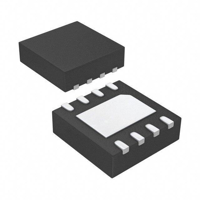
| 产品图片 |
|
| rohs | 符合RoHS无铅 / 符合限制有害物质指令(RoHS)规范要求 |
| 产品系列 | 电源管理 IC,稳压器—开关式稳压器,Fairchild Semiconductor FAN53555UC08XTinyBuck™ |
| 数据手册 | |
| 产品型号 | FAN53555UC08X |
| PWM类型 | - |
| 产品种类 | 稳压器—开关式稳压器 |
| 供应商器件封装 | 20-WLCSP |
| 关闭 | Shutdown |
| 其它名称 | FAN53555UC08XDKR |
| 包装 | Digi-Reel® |
| 单位重量 | 73 mg |
| 同步整流器 | 是 |
| 商标 | Fairchild Semiconductor |
| 商标名 | TinyBuck |
| 安装类型 | 表面贴装 |
| 安装风格 | SMD/SMT |
| 宽度 | 1.6 mm |
| 封装 | Reel |
| 封装/外壳 | 20-UFBGA,WLCSP |
| 封装/箱体 | WLCSP-20 |
| 工作温度 | -40°C ~ 85°C |
| 工作温度范围 | - 40 C to + 85 C |
| 工厂包装数量 | 3000 |
| 开关频率 | 2.4 MHz |
| 拓扑结构 | Buck |
| 最大工作温度 | + 85 C |
| 最大输入电压 | 5.5 V |
| 最小工作温度 | - 40 C |
| 最小输入电压 | 2.5 V |
| 标准包装 | 1 |
| 特色产品 | http://www.digikey.cn/product-highlights/cn/zh/fairchild-cloud-systems-computing/4301 |
| 电压-输入 | 2.5 V ~ 5.5 V |
| 电压-输出 | 0.6 V ~ 1.23 V |
| 电流-输出 | 4A |
| 电源电压-最小 | 2.5 V |
| 类型 | 降压(降压) |
| 系列 | FAN53555 |
| 负载调节 | - 0.1 %/A |
| 输入电压 | 2.5 V to 5.5 V |
| 输出数 | 1 |
| 输出电压 | 600 mV to 1.23 V |
| 输出电流 | 5 A |
| 输出端数量 | 1 Output |
| 输出类型 | 可调式 |
| 频率-开关 | 2.4MHz |


- 商务部:美国ITC正式对集成电路等产品启动337调查
- 曝三星4nm工艺存在良率问题 高通将骁龙8 Gen1或转产台积电
- 太阳诱电将投资9.5亿元在常州建新厂生产MLCC 预计2023年完工
- 英特尔发布欧洲新工厂建设计划 深化IDM 2.0 战略
- 台积电先进制程称霸业界 有大客户加持明年业绩稳了
- 达到5530亿美元!SIA预计今年全球半导体销售额将创下新高
- 英特尔拟将自动驾驶子公司Mobileye上市 估值或超500亿美元
- 三星加码芯片和SET,合并消费电子和移动部门,撤换高东真等 CEO
- 三星电子宣布重大人事变动 还合并消费电子和移动部门
- 海关总署:前11个月进口集成电路产品价值2.52万亿元 增长14.8%


PDF Datasheet 数据手册内容提取
Is Now Part of To learn more about ON Semiconductor, please visit our website at www.onsemi.com Please note: As part of the Fairchild Semiconductor integration, some of the Fairchild orderable part numbers will need to change in order to meet ON Semiconductor’s system requirements. Since the ON Semiconductor product management systems do not have the ability to manage part nomenclature that utilizes an underscore (_), the underscore (_) in the Fairchild part numbers will be changed to a dash (-). This document may contain device numbers with an underscore (_). Please check the ON Semiconductor website to verify the updated device numbers. The most current and up-to-date ordering information can be found at www.onsemi.com. Please email any questions regarding the system integration to Fairchild_questions@onsemi.com. ON Semiconductor and the ON Semiconductor logo are trademarks of Semiconductor Components Industries, LLC dba ON Semiconductor or its subsidiaries in the United States and/or other countries. ON Semiconductor owns the rights to a number of patents, trademarks, copyrights, trade secrets, and other intellectual property. A listing of ON Semiconductor’s product/patent coverage may be accessed at www.onsemi.com/site/pdf/Patent-Marking.pdf. ON Semiconductor reserves the right to make changes without further notice to any products herein. ON Semiconductor makes no warranty, representation or guarantee regarding the suitability of its products for any particular purpose, nor does ON Semiconductor assume any liability arising out of the application or use of any product or circuit, and specifically disclaims any and all liability, including without limitation special, consequential or incidental damages. Buyer is responsible for its products and applications using ON Semiconductor products, including compliance with all laws, regulations and safety requirements or standards, regardless of any support or applications information provided by ON Semiconductor. “Typical” parameters which may be provided in ON Semiconductor data sheets and/or specifications can and do vary in different applications and actual performance may vary over time. All operating parameters, including “Typicals” must be validated for each customer application by customer’s technical experts. ON Semiconductor does not convey any license under its patent rights nor the rights of others. ON Semiconductor products are not designed, intended, or authorized for use as a critical component in life support systems or any FDA Class 3 medical devices or medical devices with a same or similar classification in a foreign jurisdiction or any devices intended for implantation in the human body. Should Buyer purchase or use ON Semiconductor products for any such unintended or unauthorized application, Buyer shall indemnify and hold ON Semiconductor and its officers, employees, subsidiaries, affiliates, and distributors harmless against all claims, costs, damages, and expenses, and reasonable attorney fees arising out of, directly or indirectly, any claim of personal injury or death associated with such unintended or unauthorized use, even if such claim alleges that ON Semiconductor was negligent regarding the design or manufacture of the part. ON Semiconductor is an Equal Opportunity/Affirmative Action Employer. This literature is subject to all applicable copyright laws and is not for resale in any manner.
F A N 5 3 5 August 2015 5 5 — 5 A , 2 . 4 M FAN53555 H ® z 5 A, 2.4 MHz, Digitally Programmable TinyBuck Regulator , D i g i t a l l y Features Description P r Fixed-Frequency Operation: 2.4 MHz The FAN53555 is a step-down switching voltage regulator og that delivers a digitally programmable output from an input r Best-in-Class Load Transient a voltage supply of 2.5 V to 5.5 V. The output voltage is m Continuous Output Current Capability: 5 A programmed through an I2C interface capable of operating up m Pulse Current Capability: 6.5 A (05 Option) to 3.4 MHz. ab Using a proprietary architecture with synchronous l 2.5 V to 5.5 V Input Voltage Range e rectification, the FAN53555 is capable of delivering 5 A T Digitally Programmable Output Voltage: continuous at over 80% efficiency, while maintaining over in 80% efficiency at load currents as low as 10 mA. Pulse y 00/01/03/05/08/18 Options: 0.6-1.23 V in 10 mV Steps B currents as high as 6.5 A can be supported by the 05 option. 04/042/09/ Options: 0.603-1.411 V in 12.826 mV Steps The regulator operates at a nominal fixed frequency of uc 23 Option: 0.60-1.3875 V in 12.5 mV Steps 2.4 MHz, which reduces the value of the external components k ™ 24 Option: 0.603-1.420 V in 12.967 mV Steps to 330 nH for the output induction and as low as 20 µF for the output capacitor. Additional output capacitance can be added R 13 Option: 0.8-1.43 V in 10 mV Steps to improve regulation during load transients without affecting e g Programmable Slew Rate for Voltage Transitions stability. Inductance up to 1.2 µH may be used with additional u I2C-Compatible Interface Up to 3.4 Mbps output capacitance. lat o At moderate and light loads, Pulse Frequency Modulation PFM Mode for High Efficiency in Light Load r (PFM) is used to operate in Power-Save Mode with a typical Quiescent Current in PFM Mode: 60 µA (Typical) quiescent current of 60 µA. Even with such a low quiescent current, the part exhibits excellent transient response during Internal Soft-Start large load swings. At higher loads, the system automatically Input Under-Voltage Lockout (UVLO) switches to fixed-frequency control, operating at 2.4 MHz. In Shutdown Mode, the supply current drops below 1 µA, Thermal Shutdown and Overload Protection reducing power consumption. PFM Mode can be disabled if 20-Bump Wafer-Level Chip Scale Package (WLCSP) constant frequency is desired. The FAN53555 is available in a 20-bump, 1.6 x 2 mm, WLCSP. Applications PVIN Application, Graphic, and DSP Processors C C ARM™, Krait™, OMAP™, NovaThor™, ARMADA™ EN IN1 IN Hard Disk Drives SDA VOUT Tablets, Netbooks, Ultra-Mobile PCs SCL FAN53555 SW L1 VDD Smart Phones C VSEL OUT Core GND Gaming Devices Processor (System Load) AGND GND Figure 1. Typical Application All trademarks are the property of their respective owners. © 2010 Fairchild Semiconductor Corporation www.fairchildsemi.com FAN53555 • Rev. 1.14
F A N Ordering Information 5 3 5 Power-Up Max. Max. 5 Defaults I2C Slave A1 PIN Pulse Temperature Packing 5 Part Number RMS Package — Address Function Current Range Method VSEL0 VSEL1 Current (50 ms) 5 A FAN53555UC00X 1.05 1.20 VSEL 5 A N/A , 2 FAN53555UC01X 0.90 OFF VSEL 5 A N/A . 4 FAN53555UC03X 0.90 N/A PGOOD 5 A N/A M H FAN53555UC04X 1.10 1.20 VSEL 5 A N/A z , FAN53555UC05X 0.90 OFF VSEL 5 A 6.5 A D i FAN53555BUC05X(1) 0.90 OFF VSEL 5 A 6.5 A g i t FAN53555UC08X 1.02 1.15 VSEL 4 A N/A a l l FAN53555BUC08X(1) 1.02 1.15 VSEL 4 A N/A y P FAN53555BUC09X(1) 1.10 1.10 C0 VSEL 3 A N/A WLCSP- Tape ro -40 to 85°C FAN53555UC09X 1.10 1.10 VSEL 3 A N/A 20 & Reel g r a FAN53555UC13X 1.15 1.15 VSEL 5 A N/A m FAN53555BUC13X(1) 1.15 1.15 VSEL 5 A N/A m a FAN53555UC18X 1.02 1.15 VSEL 5 A N/A b l e FAN53555BUC18X(1) 1.02 1.15 VSEL 5 A N/A T FAN53555BUC23X(1) 1.15 1.15 VSEL 5 A N/A in y FAN53555UC24X 1.225 1.212 VSEL 4 A N/A B u FAN53555BUC24X(1) 1.225 1.212 VSEL 4 A N/A c k FAN53555UC042X(2) 1.10 1.20 C4 VSEL 5 A N/A ™ Notes: R 1. The FAN53555BUC05X, FAN53555BUC08X, FAN53555BUC09X, FAN53555BUC13X, FAN53555BUC18X, e g FAN53555BUC23X, and FAN53555BUC24X, include backside lamination. u 2. The 042 option is the same as the 04 option, except the I2C slave addresses. la t o r Recommended External Components Table 1. Recommended External Components for 5 A Maximum Load Current Component Description Vendor Parameter Typ. Unit L 0.33 µH L1 330 nH Nominal See Table 2 DCR 13 m 2 Pieces; GRM21BR60J226M (Murata) C C 44 OUT 22 F, 6.3 V, X5R, 0805 C2012X5R0J226M (TDK) 1 Piece; LMK212BJ106KG-T (Taiyo Yuden) C 10 µF 10 F, 10 V, X5R, 0805 C2012X5R1A106M (TDK) C IN 2 Pieces; GRM21BR60J106M (Murata) C 20 10 F, 6.3 V, X5R, 0805 C2012X5R0J106M (TDK) GRM155R71E103K (Murata) C 10 nF, 25 V, X7R, 0402 C 10 nF IN1 C1005X7R1E103K (TDK) © 2010 Fairchild Semiconductor Corporation www.fairchildsemi.com FAN53555 • Rev. 1.14 2
F A N Table 2. Recommended Inductors for High-Current Applications 5 3 Component Dimensions 5 5 Manufacturer Part# L (nH) DCR (mΩ) I (3) L W H 5 MAXDC — Vishay IHLP1616ABERR47M01 470 20.0 5.0 4.5 4.1 1.2 5 Mag. Layers(4) MMD-04ABNR33M-M1-RU 330 12.5 7.5 4.5 4.1 1.2 A , Mag. Layers MMD-04ABNR47M-M1-RU 470 20.0 5.0 4.5 4.1 1.2 2 . 4 Inter-Technical SM1608-R33M 330 9.6 9.0 4.5 4.1 2.0 M Bournes SRP4012-R33M 330 15.0 6.7 4.7 4.2 1.2 H z Bournes SRP4012-R47M 470 20.0 5.0 4.7 4.2 1.2 , D TDK VLC5020T-R47M 470 15.0 5.4 5.0 5.0 2.0 i g Notes: it a 3. IMAXDC is the lesser current to produce 40°C temperature rise or 30% inductance roll-off. ll 4. Preferred inductor value is 330 nH and all dynamic characterization was performed with this coil. y P r o g FAN53555-24, -08, and -09 Reduced Output Current (4 A Max. RMS. for 08, and 24, 3 A r a Max. RMS for 09) Smaller Footprint Application m m The FAN53555-24, -08, and -09 were developed to provide power for core processors with high-performance graphics a acceleration in Li-Ion-powered handheld devices. These applications require a very compact solution. The smaller input and b l output capacitors in the table below assume that additional bypass capacitance exists across the battery in fairly close proximity e to the regulator(s). The C capacitors specified below are the capacitors that are required in very close proximity to VIN and T IN i PGND (see layout recommendations in Figure 2 below). n y B u c k Table 3. Recommended External Components for Lower-Current Applications with FAN53555-08-09-24 ™ Component Description Vendor Parameter Typ. Unit R e g L1 470 or 330 nH, 2016 case size See Table 4 u l -08, ,24 Option a 44 t 2 Pieces 22 F, 6.3 V, X5R, 0603 o COUT C1608X5R0J226M (TDK) C r -09 Option 22 µF 1 Piece 22 F, 6.3 V, X5R, 0603 1 Piece; C GRM155R61A106M (Murata) C 10 IN 10 F, 10 V, X5R, 0402 CIN1 10 nF, 25 V, X5R, 0201 TMK063CG100DT-F (Taiyo Yuden) C 10 nF Table 4. Recommended Inductors for Lower-Current Applications with FAN53555-08-09-24 Component Dimensions Manufacturer Part# L (nH) DCR (mΩ Typ.) I (5) L W H MAXDC Toko DFE201612R-H-R33N 330 25 3.2 2.0 1.6 1.2 Toko DFE201612C-R47N 470 40 3.2 2.0 1.6 1.2 Cyntek PIFE20161B-R47MS-39 470 30 3.1 2.0 1.6 1.2 SEMCO CIGT201610HMR47SCE 470 30 3.1 2.0 1.6 0.9 Note: 5. I is the lesser current to produce 40°C temperature rise or 30% inductance roll-off. MAXDC © 2010 Fairchild Semiconductor Corporation www.fairchildsemi.com FAN53555 • Rev. 1.14 3
F A N Layout 5 3 5 5 5 — 5 A , 2 . 4 M H z , D ig i Figure 2. Reduced-Footprint Layout t a l l y Pin Configuration P r o VSEL* EN SCL VOUT g A1 A2 A3 A4 A4 A3 A2 A1 ra m SDA AGND B4 B3 B2 B1 m B1 B2 B3 B4 a GND C4 C3 C2 C1 b l e C1 C2 C3 C4 D4 D3 D2 D1 T VIN SW in y D1 D2 D3 D4 E4 E3 E2 E1 B u A1 = VSEL for 00, 01, 04, 05, 08, 09, 13, 18, 23, 24 c E1 E2 E3 E4 k A1 = PGOOD for 03 ™ Figure 3. Top View Figure 4. Bottom View R e g u Pin Definitions l a t o Pin # Name Description r VSEL Voltage Select. When this pin is LOW, V is set by the VSEL0 register. When this pin is HIGH, V (Except - OUT OUT is set by the VSEL1 register. A1 03 Option) PGOOD Power Good. This open-drain pin pulls LOW if an overload condition occurs or soft-start is in progress. (03) Enable. The device is in Shutdown Mode when this pin is LOW. All register values are kept during shutdown. Options 00, 01, 03, 05, 08 09, 13, 18, and 23 do not reset register values when EN is raised. A2 EN The 04, 24, and 042 options reset all registers to default values when EN pin is LOW. If pulled up to a low-impedance voltage source greater than 1.8 V, use at least 100 series resistor. A3 SCL I2C Serial Clock A4 VOUT VOUT. Sense pin for VOUT. Connect to COUT. B1 SDA I2C Serial Data B2, B3, Ground. Low-side MOSFET is referenced to this pin. C and C should be returned with a minimal GND IN OUT C1 – C4 path to these pins. Analog Ground. All signals are referenced to this pin. Avoid routing high dV/dt AC currents through B4 AGND this pin. D1, D2, VIN Power Input Voltage. Connect to the input power source. Connect to C with minimal path. E1, E2 IN D3, D4, SW Switching Node. Connect to the inductor. E3, E4 © 2010 Fairchild Semiconductor Corporation www.fairchildsemi.com FAN53555 • Rev. 1.14 4
F A N Absolute Maximum Ratings 5 3 5 Stresses exceeding the absolute maximum ratings may damage the device. The device may not function or be operable above 5 the recommended operating conditions and stressing the parts to these levels is not recommended. In addition, extended 5 exposure to stresses above the recommended operating conditions may affect device reliability. The absolute maximum — ratings are stress ratings only. 5 A Symbol Parameter Min. Max. Unit , 2 IC Not Switching -0.3 7.0 .4 Voltage on SW, VIN Pins V IC Switching -0.3 6.5 M H VIN Tied without Series Resistance) -0.3 2.0 V z Voltage on EN Pin , Tied through Series Resistance of at Least 100 -0.3 VIN(6) D i Voltage on All Other Pins IC Not Switching -0.3 V (6) V g IN i t a VOUT Voltage on VOUT Pin -0.3 3.0 V ll y VINOV_SLEW Maximum Slew Rate of VIN > 6.5 V, PWM Switching 100 V/ms P Electrostatic Discharge Human Body Model per JESD22-A114 2000 ro ESD Protection Level Charged Device Model per JESD22-C101 1500 V gr a T Junction Temperature -40 +150 °C m J m T Storage Temperature -65 +150 °C STG a b T Lead Soldering Temperature, 10 Seconds +260 °C L l e Note: T 6. Lesser of 7 V or VIN+0.3 V. in y B u c k Recommended Operating Conditions ™ R The Recommended Operating Conditions table defines the conditions for actual device operation. Recommended operating e conditions are specified to ensure optimal performance to the datasheet specifications. Fairchild does not recommend g u exceeding them or designing to Absolute Maximum Ratings. l a t Symbol Parameter Min. Typ. Max. Unit o r V Supply Voltage Range 2.5 5.5 V IN I Output Current 0 5 A OUT L Inductor 0.33 µH C Input Capacitor 10 µF IN C Output Capacitor 44 µF OUT T Operating Ambient Temperature -40 +85 °C A T Operating Junction Temperature -40 +125 °C J Thermal Properties Symbol Parameter Min. Typ. Max. Unit Junction-to-Ambient Thermal Resistance(7) 38 °C/W JA Note: 7. See Thermal Considerations in the Application Information section. © 2010 Fairchild Semiconductor Corporation www.fairchildsemi.com FAN53555 • Rev. 1.14 5
F A N 5 Electrical Characteristics 3 5 5 Minimum and maximum values are at V =2.5 V to 5.5 V, T =-40°C to +85°C, unless otherwise noted. Typical values are at 5 IN A T =25°C, V =5 V, and EN=HIGH. — A IN 5 Symbol Parameter Condition Min. Typ. Max. Unit A , Power Supplies 2 . 4 I =0 60 100 µA LOAD M I Quiescent Current Q I =0, MODE Bit=1 (Forced PWM) 43 mA H LOAD z H/W Shutdown Supply Current EN=GND 0.1 5.0 µA , I D SD S/W Shutdown Supply Current EN= VIN, BUCK_ENx=0 41 75 µA ig i VUVLO Under-Voltage Lockout Threshold VIN Rising 2.35 2.45 V ta l VUVHYST Under-Voltage Lockout Hysteresis 350 mV ly P EN, VSEL, SDA, SCL r o V HIGH-Level Input Voltage 1.1 V g IH r a V LOW-Level Input Voltage 0.4 V IL m V Logic Input Hysteresis Voltage 160 mV m LHYST a IIN Input Bias Current Input Tied to GND or VIN 0.01 1.00 µA b l PGOOD (03 Option) e T IOUTL PGOOD Pull-Down Current 1 mA in y IOUTH PGOOD HIGH Leakage Current 0.01 1.00 µA B u VOUT Regulation c k I =0, Forced PWM, ™ OUT(DC) -1.5 1.5 % VOUT=VSEL0 Default Value R 2.5 V ≤ VIN ≤ 4.5 V, eg 08, 24 VOUT from Minimum to -2.0 4.0 % u Options Maximum, IOUT(DC)=0 to la 4 A, Auto PFM/PWM to r 2.5 V ≤ VIN ≤ 4.5 V, V from Minimum to 09 Option OUT -2.0 4.0 % Maximum, I =0 to V V DC Accuracy OUT(DC) REG OUT 3 A, Auto PFM/PWM 2.5 V ≤ VIN ≤ 4.5 V, 13, 18, 23 V from Minimum to OUT -2.0 4.0 % Options Maximum, I =0 to OUT(DC) 5 A, Auto PFM/PWM 2.5 V ≤ VIN ≤ 5.5 V, All Other V from Minimum to OUT -3.0 5.0 % Options Maximum, I =0 to OUT(DC) 5 A, Auto PFM/PWM V I OUT Load Regulation IOUT(DC)=1 to 5 A -0.1 %/A LOAD V VOUT Line Regulation 2.5 V ≤ VIN ≤ 5.5 V, IOUT(DC)=1.5 A 0.01 %/V IN V Transient Response ILOAD Step 0.1 A to 1.5 A, ±40 mV TRSP tr=tf=100 ns, VOUT=1.2 V Continued on the following page… © 2010 Fairchild Semiconductor Corporation www.fairchildsemi.com FAN53555 • Rev. 1.14 6
F A N 5 Electrical Characteristics 3 5 5 Minimum and maximum values are at V =2.5 V to 5.5 V, T =-40°C to +85°C, unless otherwise noted. Typical values are at 5 IN A T =25°C, V =5 V, and EN=HIGH. — A IN 5 Symbol Parameter Condition Min. Typ. Max. Unit A , Power Switch and Protection 2 . 4 RDS(ON)P P-Channel MOSFET On Resistance VIN=5 V 28 mΩ M RDS(ON)N N-Channel MOSFET On Resistance VIN=5 V 17 mΩ H z 00, 01, 03, 04, 13, 18, 23, 042 , 6.3 7.4 8.5 A D Options i g I P-MOS Peak Current Limit 05 Option 8.5 10.0 11.5 A it LIMPK a 08, 24 Options 5.0 5.9 6.8 A ll y 09 Option 4.0 4.75 5.5 P r T Thermal Shutdown 150 °C o LIMIT g THYST Thermal Shutdown Hysteresis 17 °C ra m Rising Threshold 6.15 V V Input OVP Shutdown m SDWN Falling Threshold 5.50 5.85 V a b Frequency Control l e f Oscillator Frequency 2.05 2.40 2.75 MHz T SW i n DAC y B Resolution 6 Bits u c Differential Nonlinearity(8) 0.5 LSB k ™ Timing R I2C EN=HIGH to I2C Start 100 µs e EN g Soft-Start u l a RLOAD > 5 ; to VOUT=1.2 V; to 00, 01, 03, 04, 042, 05, 09, 13, and 300 µs r 23 Options t Regulator Enable to Regulated V SS OUT 2.5 V ≤ V ≤ 4.5 V; R =2 ; to IN LOAD V =1.127 V with 1.1 V Pre-Bias 135 175 µs OUT Voltage; 08 and 18 Options R VOUT Pull-Down Resistance, Disabled EN=0 or V <V 160 Ω OFF IN UVLO Note: 8. Monotonicity assured by design. © 2010 Fairchild Semiconductor Corporation www.fairchildsemi.com FAN53555 • Rev. 1.14 7
F A N I2C Timing Specifications 5 3 Guaranteed by design. 5 5 5 Symbol Parameter Condition Min. Typ. Max. Unit — Standard Mode 100 5 Fast Mode 400 A , f SCL Clock Frequency Fast Mode Plus 1000 kHz 2 SCL . 4 High-Speed Mode, CB ≤100 pF 3400 M High-Speed Mode, CB ≤ 400 pF 1700 H z Standard Mode 4.7 , D Bus-Free Time between STOP and t Fast Mode 1.3 µs i BUF START Conditions g i Fast Mode Plus 0.5 t a l Standard Mode 4 µs ly START or REPEATED START Fast Mode 600 ns P t r HD;STA Hold Time Fast Mode Plus 260 ns o g r High-Speed Mode 160 ns a m Standard Mode 4.7 µs m Fast Mode 1.3 µs a b t SCL LOW Period Fast Mode Plus 0.5 µs l LOW e High-Speed Mode, CB ≤ 100 pF 160.0 ns Ti n High-Speed Mode, CB ≤ 400 pF 320.0 ns y B Standard Mode 4 µs u c Fast Mode 600 ns k ™ t SCL HIGH Period Fast Mode Plus 260 ns HIGH R High-Speed Mode, CB ≤ 100 pF 60 ns e g High-Speed Mode, CB ≤ 400 pF 120 ns u Standard Mode 4.7 µs la t o Fast Mode 600.0 ns r tSU;STA REPEATED START Setup Time Fast Mode Plus 260.0 ns High-Speed Mode 160.0 ns Standard Mode 250 Fast Mode 100 t Data Setup Time ns SU;DAT Fast Mode Plus 50 High-Speed Mode 10 Standard Mode 0 3.45 µs Fast Mode 0 900.00 ns t Data Hold Time Fast Mode Plus 0 450.00 ns HD;DAT High-Speed Mode, CB ≤ 100 pF 0 70.00 ns High-Speed Mode, CB ≤ 400 pF 0 150.00 ns Standard Mode 20+0.1C 1000 B Fast Mode 20+0.1C 300 B t SCL Rise Time Fast Mode Plus 20+0.1C 120 ns RCL B High-Speed Mode, CB ≤ 100 pF 10 80 High-Speed Mode, CB ≤ 400 pF 20 160 Continued on the following page… © 2010 Fairchild Semiconductor Corporation www.fairchildsemi.com FAN53555 • Rev. 1.14 8
F A N I2C Timing Specifications (Continued) 5 3 Guaranteed by design. 5 5 5 Symbol Parameter Condition Min. Typ. Max. Unit — Standard Mode 20+0.1CB 300 5 Fast Mode 20+0.1C 300 A B , t SCL Fall Time Fast Mode Plus 20+0.1C 120 ns 2 FCL B . 4 High-Speed Mode, CB ≤ 100 pF 10 40 M High-Speed Mode, CB ≤ 400 pF 20 80 H z Rise Time of SCL After a High-Speed Mode, CB ≤ 100 pF 10 80 , D t REPEATED START Condition and ns RCL1 After ACK Bit High-Speed Mode, CB ≤ 400 pF 20 160 ig i t Standard Mode 20+0.1C 1000 a B l l y Fast Mode 20+0.1C 300 B P t SDA Rise Time Fast Mode Plus 20+0.1C 120 ns r RDA B o High-Speed Mode, CB ≤ 100 pF 10 80 gr a High-Speed Mode, CB ≤ 400 pF 20 160 m Standard Mode 20+0.1C 300 m B a Fast Mode 20+0.1CB 300 b l t SDA Fall Time Fast Mode Plus 20+0.1C 120 ns e FDA B T High-Speed Mode, CB ≤ 100 pF 10 80 in y High-Speed Mode, CB ≤ 400 pF 20 160 B Standard Mode 4 µs u c k Fast Mode 600 ns ™ t Stop Condition Setup Time SU;STO Fast Mode Plus 120 ns R High-Speed Mode 160 ns e g C Capacitive Load for SDA and SCL 400 pF u B l a t o r © 2010 Fairchild Semiconductor Corporation www.fairchildsemi.com FAN53555 • Rev. 1.14 9
F A N 5 Timing Diagrams 3 5 5 5 — tF tSU;STA tBUF 5 A SDA , 2 tR T .4 SU;DAT t M t HD;STO SCL t HIGH H LOW z tHD;STA tHD;DAT tHD;STA , D REPEATED ig START START STOP START it a Figure 5. I2C Interface Timing for Fast Plus, Fast, and Slow Modes ll y P r o g REPEATED r STOP a tFDA tRDA tSU;DAT START m m SDAH a b tSU;STA tRCL1 tFCL tRCL tSU;STO le t T SCLH tLOW HIGH in t t y HD;STA HD;DAT B REPEATED note A u START c k ™ = MCS Current Source Pull-up R e g = R Resistor Pull-up u P l a Note A: First rising edge of SCLH after Repeated Start and after each ACK bit. to r Figure 6. I2C Interface Timing for High-Speed Mode © 2010 Fairchild Semiconductor Corporation www.fairchildsemi.com FAN53555 • Rev. 1.14 10
F A N Typical Characteristics 5 3 5 Unless otherwise specified, Auto PFM/PWM, V = 3.6 V, V = 1.2 V, SCL = SDA = VSEL = EN = 1.8 V, T = 25°C; circuit IN OUT A 5 and components according to Figure 1 and Table 1. 5 — 92% 92% 5 2.7 VIN -40C A 90% 3.6 VIN 90% +25C , 5.0 VIN +85C 2 88% 88% . 4 ncy 86% ncy 86% MH Efficie 84% Efficie 84% z, 82% 82% D i g 80% 80% i t a 78% 78% l l y 76% 76% P 0 1000 2000 3000 4000 5000 0 1000 2000 3000 4000 5000 r o Load Current (mA) Load Current (mA) g r Figure 7. Efficiency vs. Load Current and Input Voltage Figure 8. Efficiency vs. Load Current and Temperature a m m 90% 90% 2.7 VIN a 88% 88% b 3.6 VIN l 86% 5.0 VIN 86% e T 84% 84% i n Efficiency 788802%%% Efficiency 788802%%% yBuc k 76% 76% ™ 74% 74% -40C R 72% 72% +25C e +85C g 70% 70% u 0 1000 2000 3000 4000 5000 0 1000 2000 3000 4000 5000 l a Load Current (mA) Load Current (mA) to r Figure 9. Efficiency vs. Load Current and Input Voltage, Figure 10. Efficiency vs. Load Current and Temperature, V =0.9 V V =5 V, V =1.2 V OUT IN OUT 90% 90% 2.7 VIN 3.6 VIN 85% 85% 5.0 VIN 80% 80% y y c c n n cie 75% cie 75% Effi Effi 70% 70% 3.6VIN, 1.2VOUT, L=MMD-04ABNR33M 3.6VIN, 1.2VOUT, L=VLC5020T-R47M 5.0VIN, 1.2VOUT, L=MMD-04ABNR33M 65% 65% 5.0VIN, 1.2VOUT, L=VLC5020T-R47M 5.0VIN, 0.9VOUT, L=MMD-04ABNR33M 5.0VIN, 0.9VOUT, L=VLC5020T-R47M 60% 60% 0 1000 2000 3000 4000 5000 0 1000 2000 3000 4000 5000 6000 7000 Load Current (mA) Load Current (mA) Figure 11. Efficiency vs. Load Current and Input Voltage, Figure 12. Efficiency vs. Load Current, V =3.6 V and 5 V, IN V =0.6 V V =1.2 V and 0.9 V OUT OUT © 2010 Fairchild Semiconductor Corporation www.fairchildsemi.com FAN53555 • Rev. 1.14 11
F A N Typical Characteristics (Continued) 5 3 5 Unless otherwise specified, Auto PFM/PWM, V = 3.6 V, V = 1.2 V, SCL = SDA = VSEL = EN = 1.8 V, T = 25°C; circuit IN OUT A 5 and components according to Figure 1 and Table 1. 5 — 25 20 2.7 VIN 2.7 VIN 5 3.6 VIN 3.6 VIN A 5.0 VIN 5.0 VIN , 20 16 2 . 4 V) 15 V) 12 M m m H Shift ( 10 Shift ( 8 z, T T D U U VO VO ig 5 4 it a l l y 0 0 0 1000 2000 3000 4000 5000 0 1000 2000 3000 4000 5000 P r Load Current (mA) Load Current (mA) o g r Figure 13. Output Regulation vs. Load Current and Input Figure 14. Output Regulation vs. Load Current and Input a Voltage, V =1.2 V Voltage, V =0.9 V m OUT OUT m 1,000 a 1,000 b l e T 800 i A) A) 800 n m m y nt ( nt ( B e e u d Curr 600 d Curr 600 ck a a ™ o o L L 400 R 400 PFM Exit e PFM Exit g PFM Enter u 2002.5 3.0 3.5 4.0 4.5 5.0 5.5 2002.5 3.0 3.5 4.0 4.5 5.0PFM Enter5.5 lato Input Voltage (V) Input Voltage (V) r Figure 15. PFM Entry / Exit Level vs. Input Voltage, Figure 16. PFM Entry / Exit Level vs. Input Voltage, VOUT=1.2 V VOUT=0.9 V 25 3,000 3.6VIN, 1.2VOUT, Auto 3.6VIN, 1.2VOUT, PWM 20 55..00VVIINN,, 11..22VVOOUUTT,, APuWtoM Hz) 2,500 mVpp) 15 5.0VIN, 0.9VOUT, Auto ncy (K 2,000 ut Ripple ( 10 ng Freque 1,500 Outp witchi 1,000 3.6VIN, 1.2VOUT, Auto 5 S 3.6VIN, 0.9VOUT, Auto 500 5.0VIN, 1.2VOUT, Auto 5.0VIN, 0.9VOUT, Auto 0 0 0 1000 2000 3000 4000 5000 0 1000 2000 3000 4000 5000 Load Current (mA) Load Current (mA) Figure 17. Output Ripple vs. Load Current, VIN=5 V and Figure 18. Frequency vs. Load Current, VIN=5 V and 3.6 V, 3.6 V, VOUT=1.2 V and 0.9 V, Auto and FPWM VOUT=1.2 V and 0.9 V, Auto PWM © 2010 Fairchild Semiconductor Corporation www.fairchildsemi.com FAN53555 • Rev. 1.14 12
F A N Typical Characteristics (Continued) 5 3 5 Unless otherwise specified, Auto PFM/PWM, VIN = 3.6 V, VOUT = 1.2 V, SCL = SDA = VSEL = EN = 1.8 V, TA = 25°C; circuit and 5 components according to Figure 1 and Table 1. 5 — 80 60 5 A 70 50 , 2 . urrent (A) 5600 urrent (mA) 3400 4 MHz Supply C 40 Input C 20 , Dig nput 30 -40C 10 -40C ita I +25C +25C ll +85C +85C y 20 0 2.5 3.0 3.5 4.0 4.5 5.0 5.5 2.5 3.0 3.5 4.0 4.5 5.0 5.5 P r o Input Supply Voltage (V) Input Voltage (V) g r Figure 19. Quiescent Current vs. Input Voltage and Figure 20. Quiescent Current vs. Input Voltage and a m Temperature, Auto PWM Temperature, FPWM m a 60 70 b 3.6VIN, 1.2VOUT, 2A Load l e 50 60 3.6VIN, 0.9VOUT, 2A Load T 5.0VIN, 0.9VOUT, 18mA Load, PFM in A) 40 y nt ( dB) 50 Bu Input Curre 2300 EEENNN___BBBUUUCCCKKK===000,,, ++-428055CCC PSRR ( 40 ck™ R EN=0, +25C 30 e 10 g u l 0 20 a 2.5 3.0 3.5 4.0 4.5 5.0 5.5 10 100 1,000 10,000 100,000 t o Input Voltage (V) Frequency (Hz) r Figure 21. Shutdown Current vs. Input Voltage Figure 22. PSRR vs. Frequency and Temperature Figure 23. Line Transient, 3-4 V , 1.2 V , 10 µs Edge, Figure 24. Line Transient, 3-4 V , 1.2 V , 10 µs Edge, IN OUT IN OUT 50 Ω Load 1 A Load © 2010 Fairchild Semiconductor Corporation www.fairchildsemi.com FAN53555 • Rev. 1.14 13
F A N Typical Characteristics (Continued) 5 3 5 Unless otherwise specified, Auto PFM/PWM, VIN = 3.6 V, VOUT = 1.2 V, SCL = SDA = VSEL = EN = 1.8 V, TA = 25°C; circuit and 5 components according to Figure 1 and Table 1. 5 — 5 A , 2 . 4 M H z , D i g i t a l l y P r o g Figure 25. Load Transient, 5 V , 0.9 V , 0.3-3 A, Figure 26. Load Transient, 3.6 V , 1.2 V , 0.3-3 A, IN OUT IN OUT r 100 ns Edge 100 ns Edge a m m a b l e T i n y B u c k ™ R e g u l a t o r Figure 27. Load Transient, 3.6 V , 1.2 V , 0.3-3 A, Figure 28. Load Transient, 3.6 V , 1.2 V , 1.5-6 A, IN OUT IN OUT 100 ns Edge, C =4x22 µF 100 ns Edge, C =4x22 µF OUT OUT Figure 29. Input Over-Voltage Protection © 2010 Fairchild Semiconductor Corporation www.fairchildsemi.com FAN53555 • Rev. 1.14 14
F A N Typical Characteristics (Continued) 5 3 5 Unless otherwise specified, Auto PFM/PWM, VIN = 3.6 V, VOUT = 1.2 V, SCL = SDA = VSEL = EN = 1.8 V, TA = 25°C; circuit and 5 components according to Figure 1 and Table 1. 5 — 5 A , 2 . 4 M H z , D i g i t a l l y P r o g r Figure 30. Startup / Shutdown, No Load, VOUT=0.9 V Figure 31. Startup / Shutdown, 180 m Load, VOUT=0.9 V a m m a b l e T i n y B u c k ™ R e g u l a t o r Figure 32. Overload Protection and Recovery Figure 33. Startup into Faulted Load, V =0.9 V OUT © 2010 Fairchild Semiconductor Corporation www.fairchildsemi.com FAN53555 • Rev. 1.14 15
F A N Operation Description 5 3 5 The FAN53555 is a step-down switching voltage regulator that output voltage. Synchronous rectification is inhibited during 5 delivers a programmable output voltage from an input voltage soft-start, allowing the IC to start into a pre-charged 5 supply of 2.5 V to 5.5 V. Using a proprietary architecture with capacitive load. — synchronous rectification, the FAN53555 is capable of If large output capacitance values are used, the regulator may 5 delivering 5 A at over 80% efficiency. Pulse currents as high fail to start. Maximum C capacitance for successfully starting A as 6.5 A can be supported by the 05 option. The regulator OUT , operates at a nominal frequency of 2.4 MHz at full load, which with a heavy constant-current load is approximately: 2 . rtheed uocuetsp utht ein vdaulcuteo r oaf nthde 2 e2x µteFr nfoarl cthoem poountpeuntt sc atop a3c3it0o rn. HH ifgohr C I I 320 (1) 4 M efficiency is maintained at light load with single-pulse PFM. OUTMAX LIMPK LOAD VOUT H where C is expressed in F and I is the load z The FAN53555 integrates an I2C-compatible interface, current dOuUriTnMgA Xsoft-start, expressed in A. LOAD , D allowing transfers up to 3.4 Mbps. This communication i g interface can be used to: If the regulator is at its current limit for 16 consecutive current i t limit cycles, the regulator shuts down and enters 3-state a Dynamically re-program the output voltage in 10 mV, l 12.826 mV increments (option 04, 09, and 042), before reattempting soft-start 1700 ms later. This limits the ly 12.5 mV increments (option 23), or 12.967 mV duty cycle of full output current during soft-start to prevent P excessive heating. r increments (option 24); o g Reprogram the mode to enable or disable PFM; The IC allows for software enable of the regulator, when EN is r HIGH, through the BUCK_EN bits. BUCK_EN0 and a Control voltage transition slew rate; or m BUCK_EN1 are both initialized HIGH in the 00, 04, 08, 09, 23, m Enable / disable the regulator. 24, and 042 options. These options start after a POR a Control Scheme regardless of the state of the VSEL pin. b l e The FAN53555 uses a proprietary non-linear, fixed-frequency In the 01 and 05 options, BUCK_EN0 and BUCK_EN1 are T PWM modulator to deliver a fast load transient response, initialized to 10. Using these options, VSEL must be LOW in while maintaining a constant switching frequency over a wide after a POR if the IC is powering the processor used to y range of operating conditions. The regulator performance is communicate through I2C. The 03 option has the VSEL input B independent of the output capacitor ESR, allowing for the use to the modulator logic internally tied LOW. uc of ceramic output capacitors. Although this type of operation k Table 5. Hardware and Software Enable ™ normally results in a switching frequency that varies with input voltage and load current, an internal frequency loop holds the Pins BITS R switching frequency constant over a large range of input e EN VSEL BUCK_EN0 BUCK_EN1 Output g voltages and load currents. u 0 X X X OFF la For very light loads, the FAN53555 operates in Discontinuous t Current Diode (DCM) single-pulse PFM, which produces low 1 0 0 X OFF o r output ripple compared with other PFM architectures. 1 0 1 X ON Transition between PWM and PFM is relatively seamless, 1 1 X 0 OFF providing a smooth transition between DCM and CCM Modes. 1 1 X 1 ON PFM can be disabled by programming the MODE bit HIGH in the VSEL registers. VSEL Pin and I2C Programming Output Voltage Enable and Soft-Start The output voltage is set by the NSELx control bits in VSEL0 When the EN pin is LOW; the IC is shut down, all internal and VSEL1 registers. The output voltage for options 00, 01, circuits are off, and the part draws very little current. In this 03, 05, 08, and 18 is given as: state, I2C cannot be written to or read from. For all options except the 04, 24, and 042 options, all register values are kept V 0.60VNSELx10mV (2) OUT while EN pin is LOW. For the 04, 24 and 042 options; registers are reset to default values when EN pin is LOW. For all For example, when NSEL = 011111 (31 decimal), then V = OUT options, registers are reset to default values during a Power 0.60 + 0.310 = 0.91 V. On Reset (POR). For the 04, 042, and 09 options; the output voltage is given as: When the OUTPUT_DISCHARGE bit in the CONTROL V 0.603VNSELx12.826mV (3) register is enabled (logic HIGH) and the EN pin is LOW or the OUT BUCK_ENx bit is LOW, a load is connected from VOUT to For the 13 option, the output voltage is given as: GND to discharge the output capacitors. V 0.80VNSELx10mV (4) Raising EN while the BUCK_ENx bit is HIGH activates the OUT part and begins the soft-start cycle. During soft-start, the modulator’s internal reference is ramped slowly to minimize surge currents on the input and prevent overshoot of the © 2010 Fairchild Semiconductor Corporation www.fairchildsemi.com FAN53555 • Rev. 1.14 16
F A N For the 23 option, the output voltage is given as: Power Good (03 Option) 5 3 V 0.60VNSELx12.5mV (5) The PGOOD pin is an open-drain output indicating that the 5 OUT regulator is enabled when its state is HIGH. PGOOD pulls 5 5 LOW under the following conditions: — For the 24 option, the output voltage is given as: Regulator is disabled (EN pin LOW, disabled by I2C, fault 5 V 0.603VNSELx12.967mV (6) time-out, UVLO, OVP, over-temperature); A OUT , Regulator is performing a soft-start. 2 Output voltage can also be controlled by toggling the VSEL . 4 pin LOW or HIGH. VSEL LOW corresponds to VSEL0 and PGOOD remains HIGH during I2C initiated VOUT transitions. M VSEL HIGH corresponds to VSEL1. Upon POR, VSEL0 and Current Limiting H VSEL1 are reset to their default voltages, shown in Table 9. z A heavy load or short circuit on the output causes the current , Transition Slew Rate Limiting D in the inductor to increase until a maximum current threshold i g When transitioning from a low to high voltage, the IC can be is reached in the high-side switch. Upon reaching this point, i t programmed for one of eight possible slew rates using the the high-side switch turns off, preventing high currents from a l SLEW bits in the CONTROL register. causing damage. Sixteen consecutive current limit cycles in ly current limit cause the regulator to shut down and stay off for P Table 6. Transition Slew Rate about 1700 s before attempting a restart. r o Decimal Bin Slew Rate g Thermal Shutdown r a 0 000 64.00 mV / µs When the die temperature increases, due to a high load m 1 001 32.00 mV / µs condition and/or high ambient temperature, the output m switching is disabled until the die temperature falls sufficiently. a 2 010 16.00 mV / µs b The junction temperature at which the thermal shutdown l e 3 011 8.00 mV / µs activates is nominally 150°C with a 17°C hysteresis. T 4 100 4.00 mV / µs Monitor Register (Reg05) in y 5 101 2.00 mV / µs The Monitor register indicates of the regulation state of the IC. B u 6 110 1.00 mV / µs If the IC is enabled and is regulating, its value is (1000 0000). c k 7 111 0.50 mV / µs I2C Interface ™ The FAN53555’s serial interface is compatible with Standard, R Transitions from high to low voltage rely on the output load to Fast, Fast Plus, and HS Mode I2C-Bus® specifications. The e dtriasncshiatirogne bVeOgUiTn st,o tthhee nICew sstoept sp osiwnti.t cOhinncge uthneti l hVigh-to -hloaws FAN53555’s SCL line is an input and its SDA line is a bi- gu reached the new set point. OUT directional open-drain output; it can only pull down the bus la when active. The SDA line only pulls LOW during data reads to For options 04, 042, 09, 23, and 24 where the Dynamic and when signaling ACK. All data is shifted in MSB (bit 7) first. r Voltage Scaling (DVS) step is not 10 mV; the actual slew rate I2C Slave Address is the corresponding number shown in Table 6 scaled by the ratio of the DVS step to 10 mV. For example, the slew rate of In hex notation, the slave address assumes a 0 LS Bit. The option 13 for Bin=011 is 8.00 mV / µs X 12.5 mV / 10 mV = hex slave address is C0 for all options except -42, which has a 10.00 mV / µs. hex slave address of C4. Under-Voltage Lockout Table 7. I2C Slave Address When EN is HIGH, the under-voltage lockout keeps the part Bits from operating until the input supply voltage rises HIGH Option Hex enough to properly operate. This ensures proper operation of 7 6 5 4 3 2 1 0 the regulator during startup or shutdown. 00 to 24 C0 1 1 0 0 0 0 0 R/W Input Over-Voltage Protection (OVP) 42 C4 1 1 0 0 0 1 0 R/W When V exceeds V (about 6.2 V) the IC stops switching IN SDWN Other slave addresses can be assigned. Contact a Fairchild to protect the circuitry from internal spikes above 6.5 V. An Semiconductor representative. internal filter prevents the circuit from shutting down due to noise spikes. © 2010 Fairchild Semiconductor Corporation www.fairchildsemi.com FAN53555 • Rev. 1.14 17
F A N Bus Timing Slave Releases tSU;STA tHD;STA 5 3 As shown in Figure 34, data is normally transferred when SCL SDA ANCAKC(K0)( 1o)r SMLASD BDitR 55 is LOW. Data is clocked in on the rising edge of SCL. 5 Typically, data transitions shortly at or after the falling edge of — SCL SCL to allow ample time for the data to set up before the next 5 SCL rising edge. Figure 37. REPEATED START Timing A , Data change allowed 2 . 4 SDA High-Speed (HS) Mode M H tH The protocols for High-Speed (HS), Low-Speed (LS), and z SCL tSU Ffoar sHt-SS pmeeodd e( FisS )3 .M4 oMdHesz . aHreS idMeondtiec aisl, eenxcteerpetd thweh ebnu st hsep ebeuds , D i master sends the HS master code 00001XXX after a START g Figure 34. Data Transfer Timing i condition. The master code is sent in Fast or Fast-Plus Mode t a Each bus transaction begins and ends with SDA and SCL (less than 1 MHz clock); slaves do not ACK this transmission. ll y HIGH. A transaction begins with a START condition, which is The master generates a REPEATED START condition (Figure P defined as SDA transitioning from 1 to 0 with SCL HIGH, as 35) that causes all slaves on the bus to switch to HS Mode. ro shown in Figure 35. The master then sends I2C packets, as described above, g r using the HS Mode clock rate and timing. a m SDA tHD;STA Slave Address The bus remains in HS Mode until a STOP bit (Figure 36) is m MS Bit sent by the master. While in HS Mode, packets are separated a by REPEATED START conditions (Figure 37). b l e SCL T Read and Write Transactions in Figure 35. START Bit y B The following figures outline the sequences for data read and A transaction ends with a STOP condition, which is defined as u write. Bus control is signified by the shading of the packet, c SDA transitioning from 0 to 1 with SCL HIGH, as shown in k Figure 36. defined as Master Drives Bus and Slave Drives Bus . ™ All addresses and data are MSB first. R Slave Releases Master Drives tHD;STO Table 8. I2C Bit Definitions for Figure 38 & Figure 39 eg ACK(0) or u SDA NACK(1) Symbol Definition la t o R REPEATED START, see Figure 37 r SCL P STOP, see Figure 36 S START, see Figure 35 Figure 36. STOP Bit ACK. The slave drives SDA to 0 to A During a read from the FAN53555, the master issues a acknowledge the preceding packet. REPEATED START after sending the register address, and NACK. The slave sends a 1 to NACK the before resending the slave address. The REPEATED START A preceding packet. is a 1 to 0 transition on SDA while SCL is HIGH, as shown in R REPEATED START, see Figure 37. Figure 37. P STOP, see Figure 36. 7 bits 0 8 bits 0 8 bits 0 S Slave Address 0 A Reg Addr A Data A P Figure 38. Write Transaction 7 bits 0 8 bits 0 7 bits 0 8 bits 1 S Slave Address 0 A Reg Addr A R Slave Address 1 A Data A P Figure 39. Read Transaction © 2010 Fairchild Semiconductor Corporation www.fairchildsemi.com FAN53555 • Rev. 1.14 18
F A N Register Description 5 3 5 Table 9. Register Map 5 5 POR Default — Hex Name Function Address 5 Option V Binary Hex OUT A , 00 1.050 10101101 AD 2 . 4 08, 18 1.020 10101010 AA M 01, 03, 05 0.900 10011110 9E H z , 04, 1.100 10100111 A7 D 00 VSEL0 Controls VOUT settings when VSEL pin = 0 24 1.225 10110000 B0 ig i t a 13 1.150 10100011 A3 l l y 23 1.150 10101100 AC P r 09 1.100 10100111 A7 o g r 00 1.200 11111100 FC a m 01, 05 1.000 01101000 68 m a 04, 1.200 11101111 EF b l e 24 1.212 10101111 AF T 01 VSEL1 Controls V settings when VSEL pin = 1 OUT i 08, 18 1.150 10110111 B7 n y B 13 1.150 10100011 A3 u c 23 1.150 10101100 AC k ™ 09 1.100 11100111 E7 R 00, 01, 03, e 10000000 80 g Determines whether VOUT output discharge is 04, 05, 24 u 02 CONTROL enabled and also the slew rate of positive la transitions 08, 09, 18 00000000 00 to 13, 23 10110000 B0 r 00, 13, 23, 10000000 80 24 01 10000001 81 03 10000011 83 03 ID1 Read-only register identifies vendor and chip type 04 10000100 84 05 10000101 85 08, 18 10001000 88 09 10001100 8C 04 ID2 Read-only register identifies die revision All 0000XXXX 0X 05 MONITOR Indicates device status All X0000000 X0 © 2010 Fairchild Semiconductor Corporation www.fairchildsemi.com FAN53555 • Rev. 1.14 19
F A N Bit Definitions 5 3 The following table defines the operation of each register bit. Bold indicates power-on default values. 5 5 5 Bit Name Value Description — VSEL0 R/W Register Address: 00 5 7 BUCK_EN0 1 Software buck enable. When EN pin is LOW, the regulator is off. When EN pin is HIGH, A BUCK_EN bit takes precedent. , 2 0 Allow Auto-PFM Mode during light load. . 6 MODE0 4 1 Forced PWM Mode. M 00 Option H z 101101 , D 08, 18 Options i Sets V value from 0.6 to 1.23 V in 10 mV steps (see Eq. (2)). g 101010 OUT i t a 01, 03, 05 Options l l 011110 y P 04 Option r o 100111 g 5:0 NSEL0 Sets V value from 0.603 to 1.411 V in 12.826 mV steps (see Eq. (3)). OUT r 09 Option a m 100111 m 13 Option Sets V value from 0.8 to 1.43 V in 10 mV steps (see Eq. (4)). a 100011 OUT b l e 23 Option 101100 Sets VOUT value from 0.6 to 1.3875 V in 12.5 mV steps (see Eq. (5)). Ti n 24 Option y 110000 Sets VOUT value from 0.603 to 1.42 V in 12.967 mV steps (see Eq. (6)). B u VSEL1 R/W Register Address: 01 c k 00, 04, 08, 09,13, ™ 18, 23, 24 Options R 7 BUCK_EN1 1 Software buck enable. When EN pin is LOW, the regulator is off. When EN pin is HIGH, e BUCK_EN bit takes precedent. g 01, 05 Options u 0 la t 08, 13, 18, 23, 24 o r Options Allow AUTO-PFM Mode during light load. 0 6 MODE1 00, 01, 04, 05, 09 Options Forced PWM Mode. 1 00 Option 111100 01, 05 Options Sets V value from 0.6 to 1.23 V in 10 mV steps (see Eq. (2)). 101000 OUT 08, 18 Options 110111 04 Option 101111 5:0 NSEL1 Sets V value from 0.603 to 1.411 V in 12.826 mV steps (see Eq. (3)). OUT 09 Option 100111 13 Option Sets V value from 0.8 to 1.43 V in 10 mV steps (see Eq. (4)). 100011 OUT 23 Option Sets V value from 0.6 to 1.3875 V in 12.5 mV steps (see Eq. (5)). 101100 OUT 24 Option Sets V value from 0.603 to 1.42 V in 12.967 mV steps (see Eq. (6)). 101111 OUT © 2010 Fairchild Semiconductor Corporation www.fairchildsemi.com FAN53555 • Rev. 1.14 20
F A N Bit Definitions 5 3 The following table defines the operation of each register bit. Bold indicates power-on default values. 5 5 5 Bit Name Value Description — CONTROL R/W Register Address: 02 5 08, 09, 18 Options A When the regulator is disabled, V is not discharged. 0 OUT , 2 7 OUTPUT_DISCHARGE 00, 01, 03, 04, .4 05,13, 23, 24 M When the regulator is disabled, V discharges through an internal pull-down. Options OUT H 1 z , 6:4 SLEW 000 –111 Sets the slew rate for positive voltage transitions (see Table 6). D i 011 Default value for 13 and 23 options g i t 3 Reserved 0 Always reads back 0 a l l 04, 09, 24 Options y 0 Setting to 1 resets all registers to default values. RESET P 2 r o All other options 0 Always reads back 0 g Reserved r a 1:0 Reserved 00 Always reads back 00 m m ID1 R Register Address: 03 a 7:5 VENDOR 100 Signifies Fairchild as the IC vendor b l e 4 Reserved 0 Always reads back 0 T 0000 IC Type = 00 Option (FAN53555UC00X / FAN53555BUC24X) in y 0001 IC Type = 01 Option (FAN53555UC01X) B 0011 IC Type = 03 Option (FAN53555UC03X) u c 0100 IC Type = 04 Option (FAN53555UC04X) k ™ 0100 IC Type = 042 Option (FAN53555UC042X) R 3:0 DIE_ID 0101 IC Type = 05 Option (FAN53555UC05X / FAN53555BUC05X) e g IC Type = 08, 18 Options (FAN53555UC08X / FAN53555BUC08X, FAN53555UC18X / u 1000 FAN53555BUC18X) la t 1100 IC Type = 09 Option (FAN53555UC09X / FAN53555BUC09X) o r 0000 IC Type = 13 Option (FAN53555UC13X / FAN53555BUC13X) 0000 IC Type = 23 Option (FAN53555BUC23X) ID2 R Register Address: 04 7:4 Reserved 0000 Always reads back 0000 00 Option 0011 01 Option 0011 03 Option 0011 04 Option 1111 3:0 DIE_REV IC mask revision 24-Option 0100 042 Option 1111 05 Option 0011 08, 18 Options 0001 © 2010 Fairchild Semiconductor Corporation www.fairchildsemi.com FAN53555 • Rev. 1.14 21
F A N Bit Definitions 5 3 The following table defines the operation of each register bit. Bold indicates power-on default values. 5 5 5 Bit Name Value Description — BUC08, BUC18 5 Options A 1111 , 2 09 Option . 4 1111 M 13 Option H 1111 z , 23 Option D i 1100 g i t MONITOR R Register Address: 05 a l l 7 PGOOD 0 1: buck is enabled and soft-start is completed y P 6:0 Not used 000 0000 Always reads back 000 0000 r o g r a m m a b l e T i n y B u c k ™ R e g u l a t o r © 2010 Fairchild Semiconductor Corporation www.fairchildsemi.com FAN53555 • Rev. 1.14 22
F A N Application Information 5 3 5 Selecting the Inductor Increasing C has negligible effect on loop stability and OUT 5 can be increased to reduce output voltage ripple or to 5 The output inductor must meet both the required inductance improve transient response. Output voltage ripple, ∆V , is — and the energy-handling capability of the application. The OUT calculated by: inductor value affects the average current limit, the output 5 vTohleta rgipep rliep pcluer,r eanntd ( t∆hIe) oeff ftihceie rnecgyu. lator is: VOUT ILfSW2CDOU1TEDSR2 8fSW1COUT (10) A, 2.4 V V V where C is the effective output capacitance. M I OUT IN OUT (7) OUT H VIN LfSW The capacitance of COUT decreases at higher output voltages, z, The maximum average load current, I is related to which results in higher ∆VOUT. Equation (10) is only valid for D MAX(LOAD), the peak current limit, ILIM(PK), by the ripple current such that: Continuous Current Mode (CCM) operation, which occurs ig when the regulator is in PWM Mode. i t I a IMAX(LOAD) ILIM(PK) (8) For large COUT values, the regulator may fail to start under lly 2 a load. If an inductor value greater than 1.0 H is used, at P The FAN53555 is optimized for operation with L=330 nH, but least 30 F of COUT should be used to ensure stability. ro is stable with inductances up to 1.0 H (nominal). The g The lowest ∆V is obtained when the IC is in PWM Mode inductor should be rated to maintain at least 80% of its value and, therefore,O UoTperating at 2.4 MHz. In PFM Mode, f is ra at I . Failure to do so lowers the amount of DC current SW m LIM(PK) reduced, causing ∆V to increase. the IC can deliver. OUT m ESL Effects a Efficiency is affected by the inductor DCR and inductance b value. Decreasing the inductor value for a given physical The Equivalent Series Inductance (ESL) of the output le size typically decreases the DCR; but since ∆I increases, the capacitor network should be kept low to minimize the square- T RMS current increases, as do core and skin-effect losses. wave component of output ripple that results from the division in ratio C ESL and the output inductor (L ). The square- y OUT OUT B IRMS IOUT(DC)2 I2 (9) wave component due to the ESL can be estimated as: uc 12 ESL k VOUT(SQ) VIN COUT (11) ™ The increased RMS current produces higher losses through L1 the R of the IC MOSFETs as well as the inductor ESR. R DS(ON) A good practice to minimize this ripple is to use multiple output e Increasing the inductor value produces lower RMS currents, capacitors to achieve the desired COUT value. For example, to gu but degrades transient response. For a given physical inductor obtain COUT=20 F, a single 22 F 0805 would produce twice la size, increased inductance usually results in an inductor with the square wave ripple as two x 10 F 0805. t o lower saturation current. r To minimize ESL, try to use capacitors with the lowest ratio of Table 10. Effects of Inductor Value (from 330 nH length to width. 0805s have lower ESL than 1206s. If low Recommended) on Regulator Performance output ripple is a chief concern, some vendors produce 0508 or 0612 capacitors with ultra-low ESL. Placing additional IMAX(LOAD) ∆VOUT (Eq.(11)) Transient Response small-value capacitors near the load also reduces the high- frequency ripple components. Increase Decrease Degraded Input Capacitor Inductor Current Rating The ceramic input capacitors should be placed as close as The current limit circuit can allow substantial peak currents to possible between the VIN pin and PGND to minimize the flow through L1 under worst-case conditions. If it is possible parasitic inductance. If a long wire is used to bring power to for the load to draw such currents, the inductor should be the IC, additional “bulk” capacitance (electrolytic or tantalum) capable of sustaining the current or failing in a safe manner. should be placed between C and the power source lead to IN reduce under-damped ringing that can occur between the For space-constrained applications, a lower current rating for inductance of the power source leads and C . L1 can be used. The FAN53555 may still protect these IN inductors in the event of a short circuit, but may not be able to The effective C capacitance value decreases as V IN IN protect the inductor from failure if the load is able to draw increases due to DC bias effects. This has no significant higher currents than the DC rating of the inductor. impact on regulator performance. Output Capacitor and V Ripple OUT Table 1 suggests 0805 capacitors, but 0603 capacitors may be used if space is at a premium. Due to voltage effects, the 0603 capacitors have a lower in-circuit capacitance than the 0805 package, which can degrade transient response and output ripple. © 2010 Fairchild Semiconductor Corporation www.fairchildsemi.com FAN53555 • Rev. 1.14 23
F A N Thermal Considerations 3. Estimate inductor copper losses using: 5 3 HPCeaBt ciso prepmero. vTehde f rjoumnc ttihoen -ItCo- athmrobuiegnht tthhee rsmoaldl erre sbiusmtapnsc et o( the) PL ILOAD2DCRL (13) 55 JA 5 is largely a function of the PCB layout (size, copper weight, 4. Determine IC losses by removing inductor losses (step 3) — and trace width) and the temperature rise from junction to from total dissipation: 5 ambient (T). P P P (14) A IC T L For the FAN53555UC, JA is 38°C/W when mounted on its , 2 four-layer evaluation board in still air with two-ounce outer . 5. Determine device operating temperature: 4 layer copper weight and one-ounce inner layers. Halving the M copper thickness results in an increased of 48°C/W. T P JA IC JA H For long-term reliable operation, the IC’s junction temperature and (15) z, (TJ) should be maintained below 125°C. TIC TA T Dig To calculate maximum operating temperature (<125°C) for a ita specific application: It is important to note that the RDS(ON) of the IC’s power ll MOSFETs increases linearly with temperature at about y 1. Use efficiency graphs to determine efficiency for the 1.21%/°C. This causes the efficiency () to degrade with P r desired VIN, VOUT, and load conditions. increasing die temperature. o g 2. Calculate total power dissipation using: ra m 1 m PT VOUTILOAD1 (12) a b l where η is efficiency from Figure 7 through Figure 12. e T i n y B u c k ™ R e g u l a t o r © 2010 Fairchild Semiconductor Corporation www.fairchildsemi.com FAN53555 • Rev. 1.14 24
F A N Layout Recommendation 5 3 5 Connect VOUT to “+’ side of COUT cap 5 5 Do not connect AGND to GND. Place via in pad of AGND — and connect directly to System GND Dedicated GND bumps for CIN and COUT, which 5 connect directly to System GND of phone board A Route all logic on this layer or inner layer , VSEL EN SCL VOUT 2 . 4 M SDA GND GND AGND H z GND GND GND GND , COUT D i CIN g CIN1 VIN VIN SW SW i t a l VIN VIN SW SW ly P r o g r a m VIN vias bring power to device m L a b l e T i n y VOUT bus should be taken from + side B u capacitor c k Figure 40. Guidance for Layer 1 ™ R e g Dedicated GND bumps for CIN and COUT, which u Route all logic on this layer or inner layer connect directly to System GND of phone board la t o r VSEL EN SCL VOUT SDA GND GND AGND GND GND GND GND VIN VIN SW SW Connect VOUT to “+’ side of COUT cap VIN VIN SW SW Figure 41. Guidance for Layer 2 © 2010 Fairchild Semiconductor Corporation www.fairchildsemi.com FAN53555 • Rev. 1.14 25
F A N 5 3 5 5 Dedicated GND bumps for CIN and COUT, which 5 connect directly to System GND of phone board — 5 A , VSEL EN SCL VOUT 2 . 4 M H SDA GND GND AGND z , D i g GND GND GND GND Connect AGND directly to this layer it a l l y P VIN VIN SW SW r o g r a VIN VIN SW SW m m a b l Dedicated System Ground e T i n y Figure 42. Guidance for Layer 3 B u c k 1. FB trace connects to “+” side of COUT cap. ™ 3. Do not place COUT near FAN53555, place cap near load R e g u l a t o r Length should be less than 0.5 inches 2. Max trace resistance between FAN53555 and CPU should not exceed 30mΩ Width (mils) Length (mils) Copper (Oz) Resistance (mΩ) 25 500 2 4.2 Table provides resistance values 25 500 1.5 4.9 for given Copper Oz. 25 500 1 5.8 25 500 0.5 7.6 Figure 43. Remote Sensing Schematic © 2010 Fairchild Semiconductor Corporation www.fairchildsemi.com FAN53555 • Rev. 1.14 26
F A N Connect VOUT to “+’ side of COUT cap 5 3 Do not connect AGND to GND. Place via in pad of AGND 5 and connect directly to System GND 5 Dedicated GND bumps for CIN and COUT, which 5 connect directly to System GND of phone board — Route all logic on this layer or inner layer VSEL EN SCL VOUT 5 A , SDA GND GND AGND 2 . 4 GND GND GND GND M H CIN z CIN1 VIN VIN SW SW , D VIN VIN SW SW ig i t a l l y P r VIN vias bring power to device o g r L a m m a b l e Length of VOUT bus leading to CPU T should be less than 0.5inches i n Figure 44. Remote Sensing Guidance, Top Layer y B u c k ™ R Product-Specific Dimensions e g u Product D E X Y Land Pattern l a t FAN53555UC00 to FAN53555UC08X, FAN53555BUC05X 2.000 ±0.03 1.600 ±0.03 0.200 0.200 Option 1 o r FAN53555BUC08X, FAN53555BUC09X, FAN53555UC09X, FAN53555UC13X, FAN53555BUC13X, FAN53555UC18X, FAN53555BUC18X, 2.015 ±0.03 1.615 ±0.03 0.2075 0.2075 Option 2 FAN53555BUC23X, FAN53555UC24X, FAN53555BUC24X, © 2010 Fairchild Semiconductor Corporation www.fairchildsemi.com FAN53555 • Rev. 1.14 27
BALLA1 E A F 1.20 1.20 INDEXAREA (cid:145)(cid:19)(cid:17)(cid:21)(cid:19) (cid:145)(cid:19)(cid:17)(cid:21)(cid:20)(cid:24) B A1 A1 CuPad CuPad 0.03 C 2X 1.60 (cid:145)(cid:19)(cid:17)(cid:22)(cid:19)(cid:3)(cid:54)(cid:82)(cid:79)(cid:71)(cid:72)(cid:85) 0.40 (cid:145)(cid:19)(cid:17)(cid:22)(cid:20)(cid:24)(cid:3)(cid:54)(cid:82)(cid:79)(cid:71)(cid:72)(cid:85) D MaskOpening MaskOpening 0.40 0.40 0.03 C option1 option2 TOPVIEW 2X RECOMMENDEDLANDPATTERN (NSMDTYPE) 0.06 C 0.625 (cid:19)(cid:17)(cid:22)(cid:26)(cid:27)(cid:147)(cid:19)(cid:17)(cid:19)(cid:20)(cid:27) 0.05 C 0.547 E (cid:19)(cid:17)(cid:21)(cid:19)(cid:27)(cid:147)(cid:19)(cid:17)(cid:19)(cid:21)(cid:20) C SEATINGPLANE SIDEVIEWS NOTES: D A.NOJEDECREGISTRATIONAPPLIES. 0.005 C A B 1.20 B.DIMENSIONSAREINMILLIMETERS. 0.40 (cid:145)(cid:19)(cid:17)(cid:21)(cid:25)(cid:19)(cid:147)(cid:19)(cid:17)(cid:19)(cid:21) C.DIMENSIONSANDTOLERANCE 20X PERASMEY14.5M,2009. E D.DATUMCISDEFINEDBYTHESPHERICAL D CROWNSOFTHEBALLS. 1.60 C E.PACKAGENOMINALHEIGHTIS586MICRONS B (cid:11)(cid:60)(cid:12)(cid:3)(cid:147)(cid:19)(cid:17)(cid:19)(cid:20)(cid:27) 0.40 (cid:3)(cid:3)(cid:3)(cid:3)(cid:147)(cid:22)(cid:28)(cid:3)(cid:48)(cid:44)(cid:38)(cid:53)(cid:50)(cid:49)(cid:54)(cid:3)(cid:11)(cid:24)(cid:23)(cid:26)(cid:16)(cid:25)(cid:21)(cid:24)(cid:3)(cid:48)(cid:44)(cid:38)(cid:53)(cid:50)(cid:49)(cid:54)(cid:12)(cid:17) A F.FORDIMENSIONSD,E,X,ANDYSEE F 1 2 3 4 PRODUCTDATASHEET. (cid:11)(cid:59)(cid:12)(cid:3)(cid:147)(cid:19)(cid:17)(cid:19)(cid:20)(cid:27) G.DRAWINGFILNAME:MKT-UC020AArev4. BOTTOMVIEW
ON Semiconductor and are trademarks of Semiconductor Components Industries, LLC dba ON Semiconductor or its subsidiaries in the United States and/or other countries. ON Semiconductor owns the rights to a number of patents, trademarks, copyrights, trade secrets, and other intellectual property. A listing of ON Semiconductor’s product/patent coverage may be accessed at www.onsemi.com/site/pdf/Patent−Marking.pdf. ON Semiconductor reserves the right to make changes without further notice to any products herein. ON Semiconductor makes no warranty, representation or guarantee regarding the suitability of its products for any particular purpose, nor does ON Semiconductor assume any liability arising out of the application or use of any product or circuit, and specifically disclaims any and all liability, including without limitation special, consequential or incidental damages. Buyer is responsible for its products and applications using ON Semiconductor products, including compliance with all laws, regulations and safety requirements or standards, regardless of any support or applications information provided by ON Semiconductor. “Typical” parameters which may be provided in ON Semiconductor data sheets and/or specifications can and do vary in different applications and actual performance may vary over time. All operating parameters, including “Typicals” must be validated for each customer application by customer’s technical experts. ON Semiconductor does not convey any license under its patent rights nor the rights of others. ON Semiconductor products are not designed, intended, or authorized for use as a critical component in life support systems or any FDA Class 3 medical devices or medical devices with a same or similar classification in a foreign jurisdiction or any devices intended for implantation in the human body. Should Buyer purchase or use ON Semiconductor products for any such unintended or unauthorized application, Buyer shall indemnify and hold ON Semiconductor and its officers, employees, subsidiaries, affiliates, and distributors harmless against all claims, costs, damages, and expenses, and reasonable attorney fees arising out of, directly or indirectly, any claim of personal injury or death associated with such unintended or unauthorized use, even if such claim alleges that ON Semiconductor was negligent regarding the design or manufacture of the part. ON Semiconductor is an Equal Opportunity/Affirmative Action Employer. This literature is subject to all applicable copyright laws and is not for resale in any manner. PUBLICATION ORDERING INFORMATION LITERATURE FULFILLMENT: N. American Technical Support: 800−282−9855 Toll Free ON Semiconductor Website: www.onsemi.com Literature Distribution Center for ON Semiconductor USA/Canada 19521 E. 32nd Pkwy, Aurora, Colorado 80011 USA Europe, Middle East and Africa Technical Support: Order Literature: http://www.onsemi.com/orderlit Phone: 303−675−2175 or 800−344−3860 Toll Free USA/Canada Phone: 421 33 790 2910 Fax: 303−675−2176 or 800−344−3867 Toll Free USA/Canada Japan Customer Focus Center For additional information, please contact your local Email: orderlit@onsemi.com Phone: 81−3−5817−1050 Sales Representative © Semiconductor Components Industries, LLC www.onsemi.com www.onsemi.com 1
Mouser Electronics Authorized Distributor Click to View Pricing, Inventory, Delivery & Lifecycle Information: O N Semiconductor: FAN53555UC042X FAN53555UC04X FAN53555UC08X FAN53555UC01X FAN53555UC05X FAN53555UC03X FAN53555UC00X FAN53555UC09X FAN53555BUC09X FAN53555BUC08X FAN53555BUC24X FAN53555UC24X FAN53555BUC05X FAN53555UC13X FAN53555BUC23X FAN53555BUC13X FAN53555BUC18X FAN53555UC18X