ICGOO在线商城 > 集成电路(IC) > PMIC - 稳压器 - DC DC 开关稳压器 > LM2700MTX-ADJ/NOPB

 Datasheet下载
- 型号: LM2700MTX-ADJ/NOPB
- 制造商: Texas Instruments
- 库位|库存: xxxx|xxxx
- 要求:
| 数量阶梯 | 香港交货 | 国内含税 |
| +xxxx | $xxxx | ¥xxxx |
查看当月历史价格
查看今年历史价格
LM2700MTX-ADJ/NOPB产品简介:
ICGOO电子元器件商城为您提供LM2700MTX-ADJ/NOPB由Texas Instruments设计生产,在icgoo商城现货销售,并且可以通过原厂、代理商等渠道进行代购。 LM2700MTX-ADJ/NOPB价格参考¥18.45-¥33.84。Texas InstrumentsLM2700MTX-ADJ/NOPB封装/规格:PMIC - 稳压器 - DC DC 开关稳压器, 可调式 升压 开关稳压器 IC 正 1.26V 1 输出 2.55A(开关) 14-TSSOP(0.173",4.40mm 宽)。您可以下载LM2700MTX-ADJ/NOPB参考资料、Datasheet数据手册功能说明书,资料中有LM2700MTX-ADJ/NOPB 详细功能的应用电路图电压和使用方法及教程。
LM2700MTX-ADJ/NOPB 是由德州仪器(Texas Instruments)生产的一款 PMIC - DC/DC 开关稳压器。该器件具有宽输入电压范围(3V 至 24V),能够提供高达 1.5A 的连续输出电流,适用于多种降压转换场景。以下是其主要应用场景:

 1. 便携式电子设备
   LM2700MTX-ADJ/NOPB 的高效能和小尺寸设计使其非常适合用于便携式电子设备,例如:
   - 手持终端
   - 移动电源
   - 便携式医疗设备(如血糖仪、脉搏血氧仪)
   - 无线通信设备(如对讲机、蓝牙音频设备)

   在这些应用中,LM2700 提供的高效率有助于延长电池寿命,同时其可调输出电压功能可以灵活满足不同负载需求。

---

 2. 工业自动化设备
   由于 LM2700 支持较宽的输入电压范围,并具备良好的热性能,它广泛应用于工业领域,例如:
   - 工业控制器
   - 数据采集系统
   - 传感器接口模块
   - PLC(可编程逻辑控制器)供电

   在工业环境中,该器件的高可靠性和稳定性能够适应复杂的电源条件。

---

 3. 汽车电子
   LM2700 的宽输入电压范围使其适合汽车环境中的电压波动(如冷启动或负载突降)。典型应用包括:
   - 车载信息娱乐系统
   - 汽车报警器
   - GPS 导航设备
   - 车载摄像头和监控系统

   其高效的功率转换能力有助于减少热量积累,从而提高系统的整体可靠性。

---

 4. 通信设备
   在通信领域,LM2700 可以为各种设备提供稳定的电源支持,例如:
   - 小型基站
   - 网络路由器
   - 以太网供电(PoE)相关设备

   它的低纹波特性确保了信号的纯净性,避免干扰通信质量。

---

 5. 消费类电子产品
   LM2700 的灵活性和高效性能也使其成为消费类电子产品的理想选择,例如:
   - 数码相机
   - 平板电脑外设
   - 游戏控制器
   - 智能家居设备(如智能灯泡驱动电路)

   这些产品通常需要紧凑的设计和高效的电源管理,而 LM2700 正好满足这些要求。

---

 总结
LM2700MTX-ADJ/NOPB 凭借其宽输入电压范围、高效率和可调输出电压特性,广泛应用于便携式设备、工业自动化、汽车电子、通信设备以及消费类电子产品中。它的灵活性和可靠性使其成为许多电源管理解决方案的理想选择。
| 参数 | 数值 |
| 产品目录 | 集成电路 (IC) |
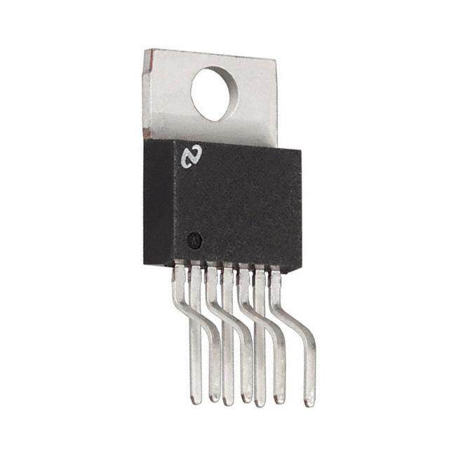
| 描述 | IC REG BOOST ADJ 2.5A 14-TSSOP |
| 产品分类 | |
| 品牌 | Texas Instruments |
| 数据手册 | |
| 产品图片 |
|
| 产品型号 | LM2700MTX-ADJ/NOPB |
| PWM类型 | 电流模式 |
| rohs | 无铅 / 符合限制有害物质指令(RoHS)规范要求 |
| 产品系列 | - |
| 供应商器件封装 | 14-TSSOP |
| 其它名称 | 296-35267-1 |
| 包装 | 剪切带 (CT) |
| 同步整流器 | 无 |
| 安装类型 | 表面贴装 |
| 封装/外壳 | 14-TSSOP(0.173",4.40mm 宽) |
| 工作温度 | -40°C ~ 125°C |
| 标准包装 | 1 |
| 电压-输入 | 2.2 V ~ 12 V |
| 电压-输出 | 1.26 V ~ 17.5 V |
| 电流-输出 | 2.5A |
| 类型 | 升压(升压) |
| 设计资源 | http://www.digikey.com/product-highlights/cn/zh/texas-instruments-webench-design-center/3176 |
| 输出数 | 1 |
| 输出类型 | 可调式 |
| 配用 | /product-detail/zh/LM2700MT-ADJEV/LM2700MT-ADJEV-ND/1640608 |
| 频率-开关 | 600kHz,1.25MHz |


- 商务部:美国ITC正式对集成电路等产品启动337调查
- 曝三星4nm工艺存在良率问题 高通将骁龙8 Gen1或转产台积电
- 太阳诱电将投资9.5亿元在常州建新厂生产MLCC 预计2023年完工
- 英特尔发布欧洲新工厂建设计划 深化IDM 2.0 战略
- 台积电先进制程称霸业界 有大客户加持明年业绩稳了
- 达到5530亿美元!SIA预计今年全球半导体销售额将创下新高
- 英特尔拟将自动驾驶子公司Mobileye上市 估值或超500亿美元
- 三星加码芯片和SET,合并消费电子和移动部门,撤换高东真等 CEO
- 三星电子宣布重大人事变动 还合并消费电子和移动部门
- 海关总署:前11个月进口集成电路产品价值2.52万亿元 增长14.8%


PDF Datasheet 数据手册内容提取
LM2700 www.ti.com SNVS152C–MAY2001–REVISEDMARCH2013 LM2700 600kHz/1.25MHz, 2.5A, Step-up PWM DC/DC Converter CheckforSamples:LM2700 FEATURES DESCRIPTION 1 • 3.6A,0.08Ω,InternalSwitch The LM2700 is a step-up DC/DC converter with a 2 3.6A, 80mΩ internal switch and pin selectable • OperatingInputVoltageRangeof2.2Vto12V operating frequency. With the ability to produce • InputUndervoltageProtection 500mA at 8V from a single Lithium Ion battery, the • AdjustableOutputVoltageupto17.5V LM2700isanidealpartforbiasingLCDdisplays.The LM2700 can be operated at switching frequencies of • 600kHz/1.25MHzPinSelectableFrequency 600kHz and 1.25MHz allowing for easy filtering and Operation low noise. An external compensation pin gives the • OverTemperatureProtection user flexibility in setting frequency compensation, • Small14-LeadTSSOPorWSONPackage which makes possible the use of small, low ESR ceramic capacitors at the output. The LM2700 APPLICATIONS features continuous switching at light loads and operates with a switching quiescent current of 2.0mA • LCDBiasSupplies at 600kHz and 3.0mA at 1.25MHz. The LM2700 is • HandheldDevices available in a low profile 14-lead TSSOP package or a14-leadWSONpackage. • PortableApplications • GSM/CDMAPhones • DigitalCameras Typical Application Circuit Figure1. 600kHzOperation 1 Pleasebeawarethatanimportantnoticeconcerningavailability,standardwarranty,anduseincriticalapplicationsof TexasInstrumentssemiconductorproductsanddisclaimerstheretoappearsattheendofthisdatasheet. Alltrademarksarethepropertyoftheirrespectiveowners. 2 PRODUCTIONDATAinformationiscurrentasofpublicationdate. Copyright©2001–2013,TexasInstrumentsIncorporated Products conform to specifications per the terms of the Texas Instruments standard warranty. Production processing does not necessarilyincludetestingofallparameters.
LM2700 SNVS152C–MAY2001–REVISEDMARCH2013 www.ti.com Connection Diagram Figure2. TopView 14-LeadTSSOPorWSON PINDESCRIPTION Pin Name Function 1 V Compensationnetworkconnection.Connectedtotheoutputofthevoltageerroramplifier. C 2 FB Outputvoltagefeedbackinput. 3 SHDN Shutdowncontrolinput,activelow. 4 AGND Analogground. 5 PGND Powerground.PGNDpinsmustbeconnectedtogetherdirectlyatthepart. 6 PGND Powerground.PGNDpinsmustbeconnectedtogetherdirectlyatthepart. 7 PGND Powerground.PGNDpinsmustbeconnectedtogetherdirectlyatthepart. 8 SW Powerswitchinput.SwitchconnectedbetweenSWpinsandPGNDpins. 9 SW Powerswitchinput.SwitchconnectedbetweenSWpinsandPGNDpins. 10 SW Powerswitchinput.SwitchconnectedbetweenSWpinsandPGNDpins. 11 NC Pinnotconnectedinternally. 12 V Analogpowerinput. IN 13 FSLCT Switchingfrequencyselectinput.V =1.25MHz.Ground=600kHz. IN 14 NC Connecttoground. 2 SubmitDocumentationFeedback Copyright©2001–2013,TexasInstrumentsIncorporated ProductFolderLinks:LM2700
LM2700 www.ti.com SNVS152C–MAY2001–REVISEDMARCH2013 Block Diagram Detailed Description TheLM2700utilizesaPWMcontrolschemetoregulatetheoutputvoltageoverallloadconditions.Theoperation can best be understood referring to the block diagram and Figure 17 of the Operation section. At the start of each cycle, the oscillator sets the driver logic and turns on the NMOS power device conducting current through the inductor, cycle 1 of Figure 17(a). During this cycle, the voltage at the V pin controls the peak inductor C current. The V voltage will increase with larger loads and decrease with smaller. This voltage is compared with C the summation of the SW voltage and the ramp compensation. The ramp compensation is used in PWM architectures to eliminate the sub-harmonic oscillations that occur during duty cycles greater than 50%. Once the summation of the ramp compensation and switch voltage equals the V voltage, the PWM comparator resets the C driver logic turning off the NMOS power device. The inductor current then flows through the schottky diode to the load and output capacitor, cycle 2 of Figure 17(b). The NMOS power device is then set by the oscillator at the endoftheperiodandcurrentflowsthroughtheinductoronceagain. The LM2700 has dedicated protection circuitry running during normal operation to protect the IC. The Thermal Shutdown circuitry turns off the NMOS power device when the die temperature reaches excessive levels. The UVP comparator protects the NMOS power device during supply power startup and shutdown to prevent operation at voltages less than the minimum input voltage. The OVP comparator is used to prevent the output voltage from rising at no loads allowing full PWM operation over all load conditions. The LM2700 also features a shutdownmodedecreasingthesupplycurrentto5µA. Thesedeviceshavelimitedbuilt-inESDprotection.Theleadsshouldbeshortedtogetherorthedeviceplacedinconductivefoam duringstorageorhandlingtopreventelectrostaticdamagetotheMOSgates. Copyright©2001–2013,TexasInstrumentsIncorporated SubmitDocumentationFeedback 3 ProductFolderLinks:LM2700
LM2700 SNVS152C–MAY2001–REVISEDMARCH2013 www.ti.com Absolute Maximum Ratings(1)(2) V 12V IN SWVoltage 18V FBVoltage 7V V Voltage 0.965V≤V ≤1.565V C C SHDNVoltage(3) 7V FSLCT(3) 12V MaximumJunctionTemperature 150°C PowerDissipation(4) InternallyLimited LeadTemperature 300°C VaporPhase(60sec.) 215°C Infrared(15sec.) 220°C ESDSusceptibility(5) HumanBodyModel 2kV MachineModel 200V (1) Absolutemaximumratingsarelimitsbeyondwhichdamagetothedevicemayoccur.OperatingRatingsareconditionsforwhichthe deviceisintendedtobefunctional,butdeviceparameterspecificationsmaynotbeensured.Forensuredspecificationsandtest conditions,seetheElectricalCharacteristics. (2) IfMilitary/Aerospacespecifieddevicesarerequired,pleasecontacttheTexasInstrumentsSalesOffice/Distributorsforavailabilityand specifications. (3) ThisvoltageshouldneverexceedV . IN (4) Themaximumallowablepowerdissipationisafunctionofthemaximumjunctiontemperature,T(MAX),thejunction-to-ambientthermal J resistance,θ ,andtheambienttemperature,T .SeetheElectricalCharacteristicstableforthethermalresistance.Themaximum JA A allowablepowerdissipationatanyambienttemperatureiscalculatedusing:P (MAX)=(T −T )/θ .Exceedingthemaximum D J(MAX) A JA allowablepowerdissipationwillcauseexcessivedietemperature,andtheregulatorwillgointothermalshutdown. (5) Thehumanbodymodelisa100pFcapacitordischargedthrougha1.5kΩresistorintoeachpin.Themachinemodelisa200pF capacitordischargeddirectlyintoeachpin. Operating Conditions OperatingJunctionTemperatureRange(1) −40°Cto+125°C StorageTemperature −65°Cto+150°C SupplyVoltage 2.2Vto12V SWVoltage 17.5V (1) Alllimitsspecifiedatroomtemperature(standardtypeface)andattemperatureextremes(boldtypeface).Allroomtemperaturelimitsare 100%testedorensuredthroughstatisticalanalysis.Alllimitsattemperatureextremesareensuredviacorrelationusingstandard StatisticalQualityControl(SQC)methods.AlllimitsareusedtocalculateAverageOutgoingQualityLevel(AOQL). 4 SubmitDocumentationFeedback Copyright©2001–2013,TexasInstrumentsIncorporated ProductFolderLinks:LM2700
LM2700 www.ti.com SNVS152C–MAY2001–REVISEDMARCH2013 Electrical Characteristics SpecificationsinstandardtypefaceareforT =25°CandthosewithboldfacetypeapplyoverthefullOperating J TemperatureRange(T =−40°Cto+125°C)Unlessotherwisespecified.V =2.2VandI =0A,unlessotherwisespecified. J IN L Min Typ Max Symbol Parameter Conditions (1) (2) (1) Units I QuiescentCurrent FB=2.2V(NotSwitching) Q 1.2 2 mA FSLCT=0V FB=2.2V(NotSwitching) 1.3 2 mA FSLCT=V IN V =0V 5 20 µA SHDN V FeedbackVoltage 1.2285 1.26 1.2915 V FB I (3) SwitchCurrentLimit V =2.7V(4) 2.55 3.6 4.3 A CL IN %V /ΔV FeedbackVoltageLine 2.2V≤V ≤12.0V 0.02 0.07 %/V FB IN IN Regulation I FBPinBiasCurrent 0.5 40 B (5) nA V InputVoltageRange 2.2 12 V IN g ErrorAmpTransconductance ΔI=5µA 40 155 290 µmho m A ErrorAmpVoltageGain 135 V/V V D MaximumDutyCycle FSLCT=Ground 78 85 % MAX D MinimumDutyCycle FSLCT=Ground 15 MIN % FSLCT=V 30 IN f SwitchingFrequency FSLCT=Ground 480 600 720 kHz S FSLCT=V 1 1.25 1.5 MHz IN I ShutdownPinCurrent V =V 0.008 1 SHDN SHDN IN µA V =0V −0.5 −1 SHDN I SwitchLeakageCurrent V =18V 0.02 20 µA L SW R SwitchR (6) V =2.7V,I =2A 80 150 mΩ DSON DSON IN SW Th SHDNThreshold OutputHigh 0.9 0.6 V SHDN OutputLow 0.6 0.3 V UVP OnThreshold 1.95 2.05 2.2 V OffThreshold 1.85 1.95 2.1 V θ ThermalResistance(7) TSSOP,packageonly 150 JA °C/W WSON,packageonly 45 (1) Alllimitsspecifiedatroomtemperature(standardtypeface)andattemperatureextremes(boldtypeface).Allroomtemperaturelimitsare 100%testedorensuredthroughstatisticalanalysis.Alllimitsattemperatureextremesareensuredviacorrelationusingstandard StatisticalQualityControl(SQC)methods.AlllimitsareusedtocalculateAverageOutgoingQualityLevel(AOQL). (2) Typicalnumbersareat25°Candrepresentthemostlikelynorm. (3) Dutycycleaffectscurrentlimitduetorampgenerator. (4) Currentlimitat0%dutycycle.SeeTypicalPerformanceCharacteristicssectionforSwitchCurrentLimitvs.V IN (5) BiascurrentflowsintoFBpin. (6) Doesnotincludethebondwires.Measureddirectlyatthedie. (7) RefertoTexasInstrument'spackagingwebsiteformoredetailedthermalinformationandmountingtechniquesfortheWSONand TSSOPpackages. Copyright©2001–2013,TexasInstrumentsIncorporated SubmitDocumentationFeedback 5 ProductFolderLinks:LM2700
LM2700 SNVS152C–MAY2001–REVISEDMARCH2013 www.ti.com Typical Performance Characteristics Efficiencyvs.LoadCurrent Efficiencyvs.LoadCurrent (V =8V,f =600kHz) (V =8V,f =1.25MHz) OUT S OUT S Figure3. Figure4. Efficiencyvs.LoadCurrent Efficiencyvs.LoadCurrent (V =5V,f =600kHz) (V =12V,f =600kHz) OUT S OUT S Figure5. Figure6. SwitchCurrentLimitvs.Temperature SwitchCurrentLimitvs.V IN Figure7. Figure8. 6 SubmitDocumentationFeedback Copyright©2001–2013,TexasInstrumentsIncorporated ProductFolderLinks:LM2700
LM2700 www.ti.com SNVS152C–MAY2001–REVISEDMARCH2013 Typical Performance Characteristics (continued) R vs.V I vs.V DSON IN Q IN (I =2A) (600kHz,notswitching) SW Figure9. Figure10. I vs.V I vs.V Q IN Q IN (600kHz,switching) (1.25MHz,notswitching) Figure11. Figure12. I vs.V I vs.V Q IN Q IN (1.25MHz,switching) (Inshutdown) Figure13. Figure14. Copyright©2001–2013,TexasInstrumentsIncorporated SubmitDocumentationFeedback 7 ProductFolderLinks:LM2700
LM2700 SNVS152C–MAY2001–REVISEDMARCH2013 www.ti.com Typical Performance Characteristics (continued) Frequencyvs.V Frequencyvs.V IN IN (600kHz) (1.25MHz) Figure15. Figure16. 8 SubmitDocumentationFeedback Copyright©2001–2013,TexasInstrumentsIncorporated ProductFolderLinks:LM2700
LM2700 www.ti.com SNVS152C–MAY2001–REVISEDMARCH2013 Operation Figure17. SimplifiedBoostConverterDiagram (a)FirstCycleofOperation(b)SecondCycleOfOperation CONTINUOUS CONDUCTION MODE The LM2700 is a current-mode, PWM boost regulator. A boost regulator steps the input voltage up to a higher output voltage. In continuous conduction mode (when the inductor current never reaches zero at steady state), theboostregulatoroperatesintwocycles. In the first cycle of operation, shown in Figure 17(a), the transistor is closed and the diode is reverse biased. EnergyiscollectedintheinductorandtheloadcurrentissuppliedbyC . OUT The second cycle is shown in Figure 17(b). During this cycle, the transistor is open and the diode is forward biased.Theenergystoredintheinductoristransferredtotheloadandoutputcapacitor. Theratioofthesetwocyclesdeterminestheoutputvoltage.Theoutputvoltageisdefinedapproximatelyas: V = VIN , D' = (1-D) = VIN OUT 1-D VOUT (1) whereDisthedutycycleoftheswitch,DandD′ willberequiredfordesigncalculations. SETTING THE OUTPUT VOLTAGE The output voltage is set using the feedback pin and a resistor divider connected to the output as shown in Figure 19. The feedback pin voltage is 1.26V, so the ratio of the feedback resistors sets the output voltage accordingtothefollowingequation: V - 1.26 OUT : R = R x FB1 FB2 1.26 (2) Copyright©2001–2013,TexasInstrumentsIncorporated SubmitDocumentationFeedback 9 ProductFolderLinks:LM2700
LM2700 SNVS152C–MAY2001–REVISEDMARCH2013 www.ti.com INTRODUCTION TO COMPENSATION Figure18. (a)Inductorcurrent.(b)Diodecurrent. The LM2700 is a current mode PWM boost converter. The signal flow of this control scheme has two feedback loops,onethatsensesswitchcurrentandonethatsensesoutputvoltage. To keep a current programmed control converter stable above duty cycles of 50%, the inductor must meet certain criteria. The inductor, along with input and output voltage, will determine the slope of the current through the inductor (see Figure 18(a)). If the slope of the inductor current is too great, the circuit will be unstable above duty cycles of 50%. A 4.7µH inductor is recommended for most 600 kHz applications, while a 2.2µH inductor may be used for most 1.25 MHz applications. If the duty cycle is approaching the maximum of 85%, it may be necessary to increase the inductance by as much as 2X. See Inductor and Diode Selection for more detailed inductorsizing. TheLM2700providesacompensationpin(V )tocustomizethevoltageloopfeedback.Itisrecommendedthata C series combination of R and C be used for the compensation network, as shown in Figure 19. For any given C C application, there exists a unique combination of R and C that will optimize the performance of the LM2700 C C circuit in terms of its transient response. The series combination of R and C introduces a pole-zero pair C C accordingtothefollowingequations: 1 fZC =2SRCCC Hz (3) 1 fPC = 2S(RC + RO)CC Hz (4) 10 SubmitDocumentationFeedback Copyright©2001–2013,TexasInstrumentsIncorporated ProductFolderLinks:LM2700
LM2700 www.ti.com SNVS152C–MAY2001–REVISEDMARCH2013 where R is the output impedance of the error amplifier, approximately 850kΩ. For most applications, O performance can be optimized by choosing values within the range 5kΩ ≤ R ≤ 20kΩ (R can be up to 200kΩ if C C C is used, see High Output Capacitor ESR Compensation) and 680pF ≤ C ≤ 4.7nF. Refer to the Application C2 C Information section for recommended values for specific circuits and conditions. Refer to the COMPENSATION sectionforotherdesignrequirement. COMPENSATION This section will present a general design procedure to help insure a stable and operational circuit. The designs in this datasheet are optimized for particular requirements. If different conversions are required, some of the components may need to be changed to ensure stability. Below is a set of general guidelines in designing a stable circuit for continuous conduction operation (loads greater than approximately 100mA), in most all cases this will provide for stability during discontinuous operation as well. The power components and their effects will bedeterminedfirst,thenthecompensationcomponentswillbechosentoproducestability. INDUCTOR AND DIODE SELECTION Although the inductor sizes mentioned earlier are fine for most applications, a more exact value can be calculated. To ensure stability at duty cycles above 50%, the inductor must have some minimum value determinedbytheminimuminputvoltageandthemaximumoutputvoltage.Thisequationis: ( D)2-1 L > V0.IN1R44DS fOsN (DD')+1 (in H) D' (5) where fs is the switching frequency, D is the duty cycle, and R is the ON resistance of the internal switch DSON taken from the graph "R vs. V " in the Typical Performance Characteristics section. This equation is only DSON IN good for duty cycles greater than 50% (D>0.5), for duty cycles less than 50% the recommended values may be used.ThecorrespondinginductorcurrentrippleasshowninFigure18(a)isgivenby: V D ’i = IN (in Amps) L 2Lfs (6) The inductor ripple current is important for a few reasons. One reason is because the peak switch current will be the average inductor current (input current or I /D') plus Δi . As a side note, discontinuous operation occurs LOAD L when the inductor current falls to zero during a switching cycle, or Δi is greater than the average inductor L current. Therefore, continuous conduction mode occurs when Δi is less than the average inductor current. Care L must be taken to make sure that the switch will not reach its current limit during normal operation. The inductor must also be sized accordingly. It should have a saturation current rating higher than the peak inductor current expected.Theoutputvoltagerippleisalsoaffectedbythetotalripplecurrent. The output diode for a boost regulator must be chosen correctly depending on the output voltage and the output current. The typical current waveform for the diode in continuous conduction mode is shown in Figure 18(b). The diode must be rated for a reverse voltage equal to or greater than the output voltage used. The average current rating must be greater than the maximum load current expected, and the peak current rating must be greater than the peak inductor current. During short circuit testing, or if short circuit conditions are possible in the application, the diode current rating must exceed the switch current limit. Using Schottky diodes with lower forwardvoltagedropwilldecreasepowerdissipationandincreaseefficiency. DC GAIN AND OPEN-LOOP GAIN Since the control stage of the converter forms a complete feedback loop with the power components, it forms a closed-loop system that must be stabilized to avoid positive feedback and instability. A value for open-loop DC gain will be required, from which you can calculate, or place, poles and zeros to determine the crossover frequency and the phase margin. A high phase margin (greater than 45°) is desired for the best stability and transient response. For the purpose of stabilizing the LM2700, choosing a crossover point well below where the right half plane zero is located will ensure sufficient phase margin. A discussion of the right half plane zero and checkingthecrossoverusingtheDCgainwillfollow. Copyright©2001–2013,TexasInstrumentsIncorporated SubmitDocumentationFeedback 11 ProductFolderLinks:LM2700
LM2700 SNVS152C–MAY2001–REVISEDMARCH2013 www.ti.com INPUT AND OUTPUT CAPACITOR SELECTION The switching action of a boost regulator causes a triangular voltage waveform at the input. A capacitor is requiredtoreducetheinputrippleandnoiseforproperoperationoftheregulator.Thesizeusedisdependanton the application and board layout. If the regulator will be loaded uniformly, with very little load changes, and at lower current outputs, the input capacitor size can often be reduced. The size can also be reduced if the input of the regulator is very close to the source output. The size will generally need to be larger for applications where the regulator is supplying nearly the maximum rated output or if large load steps are expected. A minimum value of 10µF should be used for the less stressful condtions while a 33µF or 47µF capacitor may be required for higher power and dynamic loads. Larger values and/or lower ESR may be needed if the application requires very lowrippleontheinputsourcevoltage. The choice of output capacitors is also somewhat arbitrary and depends on the design requirements for output voltageripple.ItisrecommendedthatlowESR(EquivalentSeriesResistance,denotedR )capacitorsbeused ESR such as ceramic, polymer electrolytic, or low ESR tantalum. Higher ESR capacitors may be used but will require more compensation which will be explained later on in the section. The ESR is also important because it determinesthepeaktopeakoutputvoltagerippleaccordingtotheapproximateequation: ΔV ≊2Δi R (inVolts) (7) OUT L ESR A minimum value of 10µF is recommended and may be increased to a larger value. After choosing the output capacitoryoucandetermineapole-zeropairintroducedintothecontrolloopbythefollowingequations: 1 fP1 =2S(RESR + RL)COUT (in Hz) (8) 1 fZ1 = 2SRESRCOUT (in Hz) (9) Where R is the minimum load resistance corresponding to the maximum load current. The zero created by the L ESR of the output capacitor is generally very high frequency if the ESR is small. If low ESR capacitors are used it can be neglected. If higher ESR capacitors are used see the HIGH OUTPUT CAPACITOR ESR COMPENSATIONsection. RIGHT HALF PLANE ZERO A current mode control boost regulator has an inherent right half plane zero (RHP zero). This zero has the effect of a zero in the gain plot, causing an imposed +20dB/decade on the rolloff, but has the effect of a pole in the phase, subtracting another 90° in the phase plot. This can cause undesirable effects if the control loop is influenced by this zero. To ensure the RHP zero does not cause instability issues, the control loop should be designedtohaveabandwidthoflessthan½thefrequencyoftheRHPzero.Thiszerooccursatafrequencyof: V (D')2 RHPzero = 2OSU,T L (in Hz) LOAD (10) whereI isthemaximumloadcurrent. LOAD SELECTING THE COMPENSATION COMPONENTS The first step in selecting the compensation components R and C is to set a dominant low frequency pole in C C the control loop. Simply choose values for R and C within the ranges given in the INTRODUCTION TO C C COMPENSATION section to set this pole in the area of 10Hz to 500Hz. The frequency of the pole created is determinedbytheequation: 1 f = (in Hz) PC 2S(R + R )C C O C (11) where R is the output impedance of the error amplifier, approximately 850kΩ. Since R is generally much less O C than R , it does not have much effect on the above equation and can be neglected until a value is chosen to set O the zero f . f is created to cancel out the pole created by the output capacitor, f . The output capacitor pole ZC ZC P1 will shift with different load currents as shown by the equation, so setting the zero is not exact. Determine the range of f over the expected loads and then set the zero f to a point approximately in the middle. The P1 ZC frequencyofthiszeroisdeterminedby: 1 fZC = 2SCCRC (in Hz) (12) 12 SubmitDocumentationFeedback Copyright©2001–2013,TexasInstrumentsIncorporated ProductFolderLinks:LM2700
LM2700 www.ti.com SNVS152C–MAY2001–REVISEDMARCH2013 Now R can be chosen with the selected value for C . Check to make sure that the pole f is still in the 10Hz to C C PC 500Hz range, change each value slightly if needed to ensure both component values are in the recommended range. After checking the design at the end of this section, these values can be changed a little more to optimize performance if desired. This is best done in the lab on a bench, checking the load step response with different values until the ringing and overshoot on the output voltage at the edge of the load steps is minimal. This should produce a stable, high performance circuit. For improved transient response, higher values of R should be C chosen. This will improve the overall bandwidth which makes the regulator respond more quickly to transients. If more detail is required, or the most optimal performance is desired, refer to a more in depth discussion of compensatingcurrentmodeDC/DCswitchingregulators. HIGH OUTPUT CAPACITOR ESR COMPENSATION When using an output capacitor with a high ESR value, or just to improve the overall phase margin of the control loop, another pole may be introduced to cancel the zero created by the ESR. This is accomplished by adding anothercapacitor,C ,directlyfromthecompensationpinV toground,inparallelwiththeseriescombinationof C2 C R and C . The pole should be placed at the same frequency as f , the ESR zero. The equation for this pole C C Z1 follows: 1 fPC2 = 2SCC2(RC //RO) (in Hz) (13) To ensure this equation is valid, and that C can be used without negatively impacting the effects of R and C , C2 C C f mustbegreaterthan10f . PC2 ZC CHECKING THE DESIGN The final step is to check the design. This is to ensure a bandwidth of ½ or less of the frequency of the RHP zero. This is done by calculating the open-loop DC gain, A . After this value is known, you can calculate the DC crossover visually by placing a −20dB/decade slope at each pole, and a +20dB/decade slope for each zero. The point at which the gain plot crosses unity gain, or 0dB, is the crossover frequency. If the crossover frequency is less than ½ the RHP zero, the phase margin should be high enough for stability. The phase margin can also be improved by adding C as discussed earlier in the section. The equation for A is given below with additional C2 DC equationsrequiredforthecalculation: A = 20log ( RFB2 )gmROD'{[(ZcLeff)// R ]//R } (in dB) DC(DB) 10 R + R R L L FB1 FB2 DSON (14) Zc# 2fs (in rad/s) nD' (15) L Leff = (D')2 (16) 2mc n = 1+ (no unit) m1 (17) mc≊0.072fs(inV/s) (18) V R m1 # IN DSON (in V/s) L (19) where R is the minimum load resistance, V is the minimum input voltage, g is the error amplifier L IN m transconductance found in the Electrical Characteristics table, and R is the value chosen from the graph DSON "R vs.V "intheTypicalPerformanceCharacteristicssection. DSON IN Copyright©2001–2013,TexasInstrumentsIncorporated SubmitDocumentationFeedback 13 ProductFolderLinks:LM2700
LM2700 SNVS152C–MAY2001–REVISEDMARCH2013 www.ti.com LAYOUT CONSIDERATIONS The LM2700 uses two separate ground connections, PGND for the driver and NMOS power device and AGND for the sensitive analog control circuitry. The AGND and PGND pins should be tied directly together at the package. The feedback and compensation networks should be connected directly to a dedicated analog ground plane and this ground plane must connect to the AGND pin. If no analog ground plane is available then the ground connections of the feedback and compensation networks must tie directly to the AGND pin. Connecting thesenetworkstothePGNDcaninjectnoiseintothesystemandeffectperformance. The input bypass capacitor C , as shown in Figure 19, must be placed close to the IC. This will reduce copper IN trace resistance which effects input voltage ripple of the IC. For additional input voltage filtering, a 100nF bypass capacitor can be placed in parallel with C , close to the V pin, to shunt any high frequency noise to ground. IN IN The output capacitor, C , should also be placed close to the IC. Any copper trace connections for the C OUT OUT capacitor can increase the series resistance, which directly effects output voltage ripple. The feedback network, resistors R and R , should be kept close to the FB pin, and away from the inductor, to minimize copper FB1 FB2 trace connections that can inject noise into the system. Trace connections made to the inductor and schottky diode should be minimized to reduce power dissipation and increase overall efficiency. For more detail on switching power supply layout considerations see Application Note AN-1149: Layout Guidelines for Switching PowerSupplies(literaturenumberSNVA021). 14 SubmitDocumentationFeedback Copyright©2001–2013,TexasInstrumentsIncorporated ProductFolderLinks:LM2700
LM2700 www.ti.com SNVS152C–MAY2001–REVISEDMARCH2013 APPLICATION INFORMATION Figure19. 600kHzoperation,8Voutput Figure20. 1.25MHzoperation,8Voutput Figure21. 600kHzoperation,5Voutput Copyright©2001–2013,TexasInstrumentsIncorporated SubmitDocumentationFeedback 15 ProductFolderLinks:LM2700
LM2700 SNVS152C–MAY2001–REVISEDMARCH2013 www.ti.com V =3.3V,I =200mA⇝700mA⇝200mA IN OUT CH1:I 0.5A/divDCCoupled OUT CH2:V 500mV/divACCoupled OUT CH3:InductorCurrent1A/divDCCoupled 20µs/div Figure22. LoadTransientforFigure21 Figure23. 600kHzoperation,12Voutput 16 SubmitDocumentationFeedback Copyright©2001–2013,TexasInstrumentsIncorporated ProductFolderLinks:LM2700
LM2700 www.ti.com SNVS152C–MAY2001–REVISEDMARCH2013 V =3.3V,I =50mA⇝350mA⇝50mA IN OUT CH1:I 0.5A/divDCCoupled OUT CH2:V 500mV/divACCoupled OUT CH3:InductorCurrent1A/divDCCoupled 50µs/div Figure24. LoadTransientforFigure23 Figure25. TripleOutputTFTBias(600kHzoperation) Copyright©2001–2013,TexasInstrumentsIncorporated SubmitDocumentationFeedback 17 ProductFolderLinks:LM2700
LM2700 SNVS152C–MAY2001–REVISEDMARCH2013 www.ti.com V =3.3V,I =500mA IN OUT CH1:V 2V/divDCCoupled IN CH2:V 5V/divDCCoupled OUT CH3:InductorCurrent500mA/divDCCoupled 1ms/div Figure26. StartUpWaveformforFigure25 V =3.3V,I =50mA⇝375mA⇝50mA IN OUT CH1:I 0.2A/divDCCoupled OUT CH2:V 2V/divACCoupled OUT CH3:InductorCurrent1A/divDCCoupled 500µs/div Figure27. LoadTransientforFigure25,8VOutput 18 SubmitDocumentationFeedback Copyright©2001–2013,TexasInstrumentsIncorporated ProductFolderLinks:LM2700
LM2700 www.ti.com SNVS152C–MAY2001–REVISEDMARCH2013 REVISION HISTORY ChangesfromRevisionB(March2013)toRevisionC Page • ChangedlayoutofNationalDataSheettoTIformat.......................................................................................................... 18 Copyright©2001–2013,TexasInstrumentsIncorporated SubmitDocumentationFeedback 19 ProductFolderLinks:LM2700
PACKAGE OPTION ADDENDUM www.ti.com 6-Feb-2020 PACKAGING INFORMATION Orderable Device Status Package Type Package Pins Package Eco Plan Lead/Ball Finish MSL Peak Temp Op Temp (°C) Device Marking Samples (1) Drawing Qty (2) (6) (3) (4/5) LM2700LD-ADJ/NOPB ACTIVE WSON NHE 14 1000 Green (RoHS SN Level-3-260C-168 HR -40 to 125 S00001B & no Sb/Br) LM2700MT-ADJ NRND TSSOP PW 14 94 TBD Call TI Call TI -40 to 125 2700MT -ADJ LM2700MT-ADJ/NOPB ACTIVE TSSOP PW 14 94 Green (RoHS SN Level-1-260C-UNLIM -40 to 125 2700MT & no Sb/Br) -ADJ LM2700MTX-ADJ/NOPB ACTIVE TSSOP PW 14 2500 Green (RoHS SN Level-1-260C-UNLIM -40 to 125 2700MT & no Sb/Br) -ADJ (1) The marketing status values are defined as follows: ACTIVE: Product device recommended for new designs. LIFEBUY: TI has announced that the device will be discontinued, and a lifetime-buy period is in effect. NRND: Not recommended for new designs. Device is in production to support existing customers, but TI does not recommend using this part in a new design. PREVIEW: Device has been announced but is not in production. Samples may or may not be available. OBSOLETE: TI has discontinued the production of the device. (2) RoHS: TI defines "RoHS" to mean semiconductor products that are compliant with the current EU RoHS requirements for all 10 RoHS substances, including the requirement that RoHS substance do not exceed 0.1% by weight in homogeneous materials. Where designed to be soldered at high temperatures, "RoHS" products are suitable for use in specified lead-free processes. TI may reference these types of products as "Pb-Free". RoHS Exempt: TI defines "RoHS Exempt" to mean products that contain lead but are compliant with EU RoHS pursuant to a specific EU RoHS exemption. Green: TI defines "Green" to mean the content of Chlorine (Cl) and Bromine (Br) based flame retardants meet JS709B low halogen requirements of <=1000ppm threshold. Antimony trioxide based flame retardants must also meet the <=1000ppm threshold requirement. (3) MSL, Peak Temp. - The Moisture Sensitivity Level rating according to the JEDEC industry standard classifications, and peak solder temperature. (4) There may be additional marking, which relates to the logo, the lot trace code information, or the environmental category on the device. (5) Multiple Device Markings will be inside parentheses. Only one Device Marking contained in parentheses and separated by a "~" will appear on a device. If a line is indented then it is a continuation of the previous line and the two combined represent the entire Device Marking for that device. (6) Lead/Ball Finish - Orderable Devices may have multiple material finish options. Finish options are separated by a vertical ruled line. Lead/Ball Finish values may wrap to two lines if the finish value exceeds the maximum column width. Important Information and Disclaimer:The information provided on this page represents TI's knowledge and belief as of the date that it is provided. TI bases its knowledge and belief on information provided by third parties, and makes no representation or warranty as to the accuracy of such information. Efforts are underway to better integrate information from third parties. TI has taken and Addendum-Page 1
PACKAGE OPTION ADDENDUM www.ti.com 6-Feb-2020 continues to take reasonable steps to provide representative and accurate information but may not have conducted destructive testing or chemical analysis on incoming materials and chemicals. TI and TI suppliers consider certain information to be proprietary, and thus CAS numbers and other limited information may not be available for release. In no event shall TI's liability arising out of such information exceed the total purchase price of the TI part(s) at issue in this document sold by TI to Customer on an annual basis. Addendum-Page 2
PACKAGE MATERIALS INFORMATION www.ti.com 24-Aug-2017 TAPE AND REEL INFORMATION *Alldimensionsarenominal Device Package Package Pins SPQ Reel Reel A0 B0 K0 P1 W Pin1 Type Drawing Diameter Width (mm) (mm) (mm) (mm) (mm) Quadrant (mm) W1(mm) LM2700LD-ADJ/NOPB WSON NHE 14 1000 178.0 12.4 4.3 4.3 1.3 8.0 12.0 Q1 LM2700MTX-ADJ/NOPB TSSOP PW 14 2500 330.0 12.4 6.95 5.6 1.6 8.0 12.0 Q1 PackMaterials-Page1
PACKAGE MATERIALS INFORMATION www.ti.com 24-Aug-2017 *Alldimensionsarenominal Device PackageType PackageDrawing Pins SPQ Length(mm) Width(mm) Height(mm) LM2700LD-ADJ/NOPB WSON NHE 14 1000 210.0 185.0 35.0 LM2700MTX-ADJ/NOPB TSSOP PW 14 2500 367.0 367.0 35.0 PackMaterials-Page2
None
None
MECHANICAL DATA NHE0014A LDA14A (REV A) www.ti.com
IMPORTANTNOTICEANDDISCLAIMER TI PROVIDES TECHNICAL AND RELIABILITY DATA (INCLUDING DATASHEETS), DESIGN RESOURCES (INCLUDING REFERENCE DESIGNS), APPLICATION OR OTHER DESIGN ADVICE, WEB TOOLS, SAFETY INFORMATION, AND OTHER RESOURCES “AS IS” AND WITH ALL FAULTS, AND DISCLAIMS ALL WARRANTIES, EXPRESS AND IMPLIED, INCLUDING WITHOUT LIMITATION ANY IMPLIED WARRANTIES OF MERCHANTABILITY, FITNESS FOR A PARTICULAR PURPOSE OR NON-INFRINGEMENT OF THIRD PARTY INTELLECTUAL PROPERTY RIGHTS. These resources are intended for skilled developers designing with TI products. You are solely responsible for (1) selecting the appropriate TI products for your application, (2) designing, validating and testing your application, and (3) ensuring your application meets applicable standards, and any other safety, security, or other requirements. These resources are subject to change without notice. TI grants you permission to use these resources only for development of an application that uses the TI products described in the resource. Other reproduction and display of these resources is prohibited. No license is granted to any other TI intellectual property right or to any third party intellectual property right. TI disclaims responsibility for, and you will fully indemnify TI and its representatives against, any claims, damages, costs, losses, and liabilities arising out of your use of these resources. TI’s products are provided subject to TI’s Terms of Sale (www.ti.com/legal/termsofsale.html) or other applicable terms available either on ti.com or provided in conjunction with such TI products. TI’s provision of these resources does not expand or otherwise alter TI’s applicable warranties or warranty disclaimers for TI products. Mailing Address: Texas Instruments, Post Office Box 655303, Dallas, Texas 75265 Copyright © 2020, Texas Instruments Incorporated