ICGOO在线商城 > 集成电路(IC) > PMIC - 稳压器 - 线性 > TPS79225DBVR
 Datasheet下载
- 型号: TPS79225DBVR
- 制造商: Texas Instruments
- 库位|库存: xxxx|xxxx
- 要求:
| 数量阶梯 | 香港交货 | 国内含税 |
| +xxxx | $xxxx | ¥xxxx |
查看当月历史价格
查看今年历史价格
TPS79225DBVR产品简介:
ICGOO电子元器件商城为您提供TPS79225DBVR由Texas Instruments设计生产,在icgoo商城现货销售,并且可以通过原厂、代理商等渠道进行代购。 TPS79225DBVR价格参考¥3.67-¥9.06。Texas InstrumentsTPS79225DBVR封装/规格:PMIC - 稳压器 - 线性, Linear Voltage Regulator IC Positive Fixed 1 Output 2.5V 100mA SOT-23-5。您可以下载TPS79225DBVR参考资料、Datasheet数据手册功能说明书,资料中有TPS79225DBVR 详细功能的应用电路图电压和使用方法及教程。
TPS79225DBVR 是 Texas Instruments(德州仪器)推出的一款 PMIC 线性稳压器,属于 TPS792 系列。其输出电压固定为 2.5V,并具有低dropout电压和高精度的特性,适用于对电源稳定性要求较高的场景。以下是该型号的一些典型应用场景:

1. 便携式电子设备
   TPS79225DBVR 的低功耗和小封装设计使其非常适合便携式设备,例如智能手机、平板电脑、可穿戴设备(如智能手表和健身追踪器)等。这些设备通常需要稳定的电源供应以支持处理器、传感器和其他组件的运行。

2. 微控制器供电
   该稳压器能够为各种微控制器(MCU)提供稳定的工作电压。由于其输出电压为 2.5V,可以满足许多低功耗 MCU 和数字电路的需求,同时其低噪声特性有助于提高系统的信号完整性。

3. 模拟电路和传感器供电
   TPS79225DBVR 的低噪声和高 PSRR(电源抑制比)性能使其成为模拟电路和精密传感器的理想选择。例如,在音频设备、医疗设备或工业传感器中,它可以为 ADC、DAC 或其他敏感元件提供干净的电源。

4. 通信模块
   在无线通信模块(如蓝牙、Wi-Fi 或 Zigbee 模块)中,TPS79225DBVR 可以为射频(RF)部分提供稳定的电源,确保信号传输的可靠性和质量。

5. 电池供电系统
   由于其低 dropout 电压特性,TPS79225DBVR 非常适合电池供电的系统。它可以在电池电量较低时继续提供稳定的输出电压,从而延长设备的运行时间。

6. 消费类电子产品
   包括数码相机、便携式媒体播放器和其他消费类电子产品,这些设备通常需要高效且紧凑的电源解决方案,TPS79225DBVR 的 SOT-23 封装正好满足这一需求。

总之,TPS79225DBVR 凭借其高性能、小尺寸和低功耗的特点,广泛应用于需要稳定低压电源的各种电子设备中,尤其是在便携式和低功耗系统中表现出色。
| 参数 | 数值 |
| 产品目录 | 集成电路 (IC)半导体 |
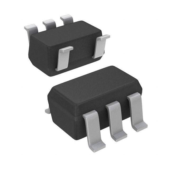
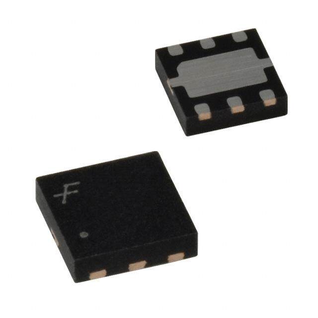
| 描述 | IC REG LDO 2.5V 0.1A SOT23-5低压差稳压器 100mA 2.5V LDO |
| 产品分类 | |
| 品牌 | Texas Instruments |
| 产品手册 | |
| 产品图片 |
|
| rohs | 符合RoHS无铅 / 符合限制有害物质指令(RoHS)规范要求 |
| 产品系列 | 电源管理 IC,低压差稳压器,Texas Instruments TPS79225DBVR- |
| 数据手册 | http://www.ti.com/lit/pdf/slvs337b |
| 产品型号 | TPS79225DBVR |
| PCN设计/规格 | |
| 产品目录页面 | |
| 产品种类 | 低压差稳压器 |
| 供应商器件封装 | SOT-23-5 |
| 其它名称 | 296-11869-1 |
| 包装 | 剪切带 (CT) |
| 商标 | Texas Instruments |
| 回动电压—最大值 | 90 mV |
| 安装类型 | 表面贴装 |
| 安装风格 | SMD/SMT |
| 封装 | Reel |
| 封装/外壳 | SC-74A,SOT-753 |
| 封装/箱体 | SOT-23-5 |
| 工作温度 | -40°C ~ 85°C |
| 工厂包装数量 | 3000 |
| 最大功率耗散 | 0.561 W |
| 最大工作温度 | + 85 C |
| 最大输入电压 | 5.5 V |
| 最小工作温度 | - 40 C |
| 最小输入电压 | + 2.7 V |
| 标准包装 | 1 |
| 电压-跌落(典型值) | - |
| 电压-输入 | 2.7 V ~ 5.5 V |
| 电压-输出 | 2.5V |
| 电压调节准确度 | 2 % |
| 电流-输出 | 100mA |
| 电流-限制(最小值) | 285mA |
| 稳压器拓扑 | 正,固定式 |
| 稳压器数 | 1 |
| 系列 | TPS79225 |
| 线路调整率 | 0.05 % / V |
| 负载调节 | 5 mV |
| 输入偏压电流—最大 | 0.17 mA |
| 输出电压 | 2.5 V |
| 输出电流 | 100 mA |
| 输出端数量 | 1 Output |
| 输出类型 | Fixed |
| 配用 | /product-detail/zh/TPS76901EVM-127/296-11030-ND/381854 |


- 商务部:美国ITC正式对集成电路等产品启动337调查
- 曝三星4nm工艺存在良率问题 高通将骁龙8 Gen1或转产台积电
- 太阳诱电将投资9.5亿元在常州建新厂生产MLCC 预计2023年完工
- 英特尔发布欧洲新工厂建设计划 深化IDM 2.0 战略
- 台积电先进制程称霸业界 有大客户加持明年业绩稳了
- 达到5530亿美元!SIA预计今年全球半导体销售额将创下新高
- 英特尔拟将自动驾驶子公司Mobileye上市 估值或超500亿美元
- 三星加码芯片和SET,合并消费电子和移动部门,撤换高东真等 CEO
- 三星电子宣布重大人事变动 还合并消费电子和移动部门
- 海关总署:前11个月进口集成电路产品价值2.52万亿元 增长14.8%


PDF Datasheet 数据手册内容提取
TPS79201, TPS79225 TPS79228, TPS79230 Actual Size Actual Size www.ti.com (3,00 mm x 3,00 mm) (3,00 mm x 3,00 mm) SLVS337B – MARCH 2001 – REVISED MAY 2002 ULTRALOW-NOISE, HIGH PSRR, FAST RF 100-mA LOW-DROPOUT LINEAR REGULATORS FEATURES DESCRIPTION (cid:1) 100-mA Low-Dropout Regulator With EN The TPS792xx family of low-dropout (LDO) (cid:1) low-power linear voltage regulators features high Available in 2.5-V, 2.8-V, 3-V, and Adj. (cid:1) power supply rejection ratio (PSRR), ultralow High PSRR (75 dB at 10 kHz) noise, fast start-up, and excellent line and load (cid:1) Ultralow Noise (27 µV) transient responses in a small outline, SOT23, (cid:1) Fast Start-Up Time (50 µs) package. Each device in the family is stable, with (cid:1) Stable With Any 1-µF Ceramic Capacitor a small 1-µF ceramic capacitor on the output. The (cid:1) family uses an advanced, proprietary BiCMOS Excellent Load/Line Transient fabrication process to yield extremely low dropout (cid:1) Very Low Dropout Voltage voltages (e.g., 55 mV at 100 mA, TPS79230). (55 mV at Full Load, TPS79230) Each device achieves fast start-up times (cid:1) 5-Pin SOT23 (DBV) Package (approximately 50 µs with a 0.001 µF bypass (cid:1) capacitor) while consuming very low quiescent TPS791xx Provides EN Options current (170 µA typical). Moreover, when the device is placed in standby mode, the supply APPLICATIONS current is reduced to less than 1 µA. The (cid:1) Cellular and Cordless Telephones TPS79228 exhibits approximately 27 µV of RMS (cid:1) VCOs output voltage noise with a 0.1 µF bypass (cid:1) capacitor. Applications with analog components RF that are noise sensitive, such as portable RF (cid:1) Bluetooth, Wireless LAN electronics, benefit from the high PSRR and low (cid:1) Handheld Organizers, PDA noise features as well as the fast response time. DBV PACKAGE TPS79228 TPS79228 (TOP VIEW) RIPPLE REJECTION OUTPUT SPECTRAL NOISE DENSITY vs vs IN 1 5 OUT FREQUENCY FREQUENCY 90 0.3 GND 2 IO = 100 mA Hz VI = 3.8 V EN 3 4 BYPASS 80 µV/ 0.25 CCo(b =yp 1) µ=F 0.1 µF B 70 GNIDN DFB(ixTVeO1 2dPP AO VCpIKEt65ioWAnG)EOFBUT Ripple Rejection – d 2563400000 VCIoI O= = 3 =1. 801 0Vµ FmA ut Spectral Noise Density – 00..0001..5512 IO = I1O0 =0 1m AmA EN 3 4 BYPASS 100 C(byp) = 0.01 µF Outp 0 10 100 1 k 10 k 100 k 1 M 10 M 100 1k 10k 100k Adjustable Option f – Frequency – Hz f – Frequency – Hz Please be aware that an important notice concerning availability, standard warranty, and use in critical applications of TexasInstruments semiconductor products and disclaimers thereto appears at the end of this data sheet. Bluetooth is a trademark owned by the Bluetooth SIG, Inc. PRODUCTION DATA information is current as of publication date. Products Copyright 2002, Texas Instruments Incorporated conform to specifications per the terms of Texas Instruments standard warranty. Production processing does not necessarily include testing of all parameters.
TPS79201, TPS79225 TPS79228, TPS79230 www.ti.com SLVS337B – MARCH 2001 – REVISED MAY 2002 These devices have limited built-in ESD protection. The leads should be shorted together or the device placed in conductive foam during storage or handling to prevent electrostatic damage to the MOS gates. ORDERING INFORMATION TJ VOLTAGE PACKAGE PART NUMBER SYMBOL 1.2 to 5.5 V TPS79201DBVT(1) TPS79201DBVR(2) PEVI 2.5 V SSOOTT2233 TPS79225DBVT(1) TPS79225DBVR(2) PEXI –4400°°CC ttoo 112255°°CC 2.8 V (DBV) TPS79228DBVT(1) TPS79228DBVR(2) PEWI 3 V TPS79230DBVT(1) TPS79230DBVR(2) PEYI (1)The DBVT indicates tape and reel of 250 parts. (2)The DBVR indicates tape and reel of 3000 parts. ABSOLUTE MAXIMUM RATINGS over operating free-air temperature range (unless otherwise noted)(1) TPS79201, TPS79225 TPS79228, TPS79230 Input voltage range (cid:2)(cid:3)(cid:4) –0.3 V to 6 V Voltage range at EN –0.3 V to VI + 0.3 V Voltage on OUT –0.3 V to 6 V Peak output current Internally limited ESD rating, HBM 2 kV ESD rating, CDM 500 V Continuous total power dissipation See Dissipation Rating Table Operating virtual junction temperature range, TJ –40°C to 150°C Operating ambient temperature range, TA –40°C to 85°C Storage temperature range, Tstg –65°C to 150°C (1)Stresses beyond those listed under “absolute maximum ratings” may cause permanent damage to the device. These are stress ratings only, and functional operation of the device at these or any other conditions beyond those indicated under “recommended operating conditions” is not implied. Exposure to absolute-maximum-rated conditions for extended periods may affect device reliability. (2)All voltage values are with respect to network ground terminal. PACKAGE DISSIPATION RATING DERATING FACTOR TA ≤ 25°C TA = 70°C TA = 85°C BOARD PACKAGE RθJC RθJA ABOVE TA = 25°C POWER RATING POWER RATING POWER RATING Low K(1) DBV 63.75°C/W 256°C/W 3.906 mW/°C 391 mW 215 mW 156 mW High K(2) DBV 63.75°C/W 178.3°C/W 5.609 mW/°C 561 mW 308 mW 224 mW (1)The JEDEC low K (1s) board design used to derive this data was a 3-inch x 3-inch, two layer board with 2 ounce copper traces on top of the board. (2)The JEDEC high K (2s2p) board design used to derive this data was a 3-inch x 3-inch, multilayer board with 1 ounce internal power and ground planes and 2 ounce copper traces on top and bottom of the board. RECOMMENDED OPERATING CONDITIONS MIN NOM MAX UNIT Input voltage, VI (1) 2.7 5.5 V Continuous output current, IO (2) 0 100 mA Operating junction temperature, TJ –40 125 °C (1)To calculate the minimum input voltage for your maximum output current, use the following formula: VI(min) = VO(max) + VDO (max load) (2)Continuous output current and operating junction temperature are limited by internal protection circuitry, but it is not recommended that the device operate under conditions beyond those specified in this table for extended periods of time. 2
TPS79201, TPS79225 TPS79228, TPS79230 www.ti.com SLVS337B – MARCH 2001 – REVISED MAY 2002 ELECTRICAL CHARACTERISTICS over recommended operating free-air temperature range, (TJ = –40 to 125°C), VI = VO(typ) + 1 V, IO = 1 mA, EN = VI, Co = 10 µF, C(byp) = 0.01 µF (unless otherwise noted) PARAMETER TEST CONDITIONS MIN TYP MAX UNIT TJ = 25°C, 1.22 V ≤ VO ≤ 5.2 VO TTPPSS7799220011 0 µA < IO < 100 mA, 1.22 V ≤ VO ≤ 5.2 V (1) 0.98 VO 1.02 VO TJ = 25°C 2.5 TTPPSS7799222255 0 µA < IO < 100 mA, 3.5 V < VI < 5.5 V 2.45 2.55 OOuuttppuutt vvoollttaaggee VV TJ = 25°C 2.8 TTPPSS7799222288 0 µA < IO < 100 mA, 3.8 V < VI < 5.5 V 2.744 2.856 TJ = 25°C 3 TTPPSS7799223300 0 µA < IO < 100 mA, 4 V < VI < 5.5 V 2.94 3.06 QQuuiieesscceenntt ccuurrrreenntt ((GGNNDD ccuurrrreenntt)) 0 µA < IO < 100 mA, TJ = 25°C 170 µµAA 0 µA < IO < 100 mA 250 Load regulation 0 µA < IO < 100 mA, TJ = 25°C 5 mV OOuuttppuutt vvoollttaaggee lliinnee rreegguullaattiioonn ((∆∆VVOO//VVOO))((22)) VVOO ++ 11 VV << VVII ≤≤ 55..55 VV,, TJ = 25°C 0.05 0.12 %%//VV C(byp) = 0.001 µF 50 OOuuttppuutt nnooiissee vvoollttaaggee ((TTPPSS7799222288)) BBIOOWW = == 1 011000 00m HHAzz,, ttToo JJ11 =0000 2 kk5HH°Czz,, CC((bbyypp)) == 00..00014 µ7F µF 3331 µµVVRRMMSS C(byp) = 0.1 µF 27 C(byp) = 0.001 µF 50 TTiimmee,, ssttaarrtt-uup ((TTPPSS7799222288)) RRTTJJL === 22225588°° CCΩΩ, CCo = 11 µFF, C(byp) = 0.0047 µF 70 µµss C(byp) = 0.01 µF 90 Output current limit VO = 0 V (1) 285 600 mA UVLO threshold VCC rising 2.25 2.65 V UVLO hysteresis TJ = 25°C VCC rising 100 mV Standby current EN = 0 V, 2.7 V < VI < 5.5 V 0.7 1 µA High level enable input voltage 2.7 V < VI < 5.5 V 2 V Low level enable input voltage 2.7 V < VI < 5.5 V 0.7 V Input current (EN) EN = 0 V –1 1 µA f = 100 Hz, TJ = 25°C, IO = 10 mA 70 f = 100 Hz, TJ = 25°C, IO = 100 mA 72 PPoowweerr ssuuppppllyy rriippppllee rreejjeeccttiioonn TTPPSS7799222288 ddBB f = 10 kHz, TJ = 25°C, IO = 100 mA 75 f = 100 kHz, TJ = 25°C, IO = 100 mA 47 IO = 100 mA, TJ = 25°C 60 TTPPSS7799222288 IO = 100 mA 110 DDropoutt vollttag((33)) mVV IO = 100 mA, TJ = 25°C 55 TTPPSS7799223300 IO = 100 mA 100 (1)The minimum IN operating voltage is 2.7 V or VO(typ) + 1 V, whichever is greater. The maximum IN voltage is 5.5 V. The maximum output current is 100 mA. (2)If VO≤ 2.5 V then VImin = 2.7 V, VImax = 5.5 V: (cid:2) (cid:4) V V (cid:6)2.7V Lineregulation(mV) (cid:1) (cid:2)%(cid:3)V(cid:4) (cid:5) O Imax (cid:5)1000 100 If VO ≥ 2.5 V then VImin = VO + 1 V, VImax = 5.5 V: (3)IN voltage equals VO(typ) – 100 mV; The TPS79225 dropout voltage is limited by the input voltage range limitations. 3
TPS79201, TPS79225 TPS79228, TPS79230 www.ti.com SLVS337B – MARCH 2001 – REVISED MAY 2002 FUNCTIONAL BLOCK DIAGRAM—ADJUSTABLE VERSION VIN VOUT UVLO Current Sense SHUTDOWN ILIM R1 GND _ + FB EN R2 UVLO Thermal Shutdown External to the Device Bandgap 250 kΩ Vref VIN Reference Bypass FUNCTIONAL BLOCK DIAGRAM—FIXED VERSION VIN VOUT UVLO Current Sense GND SHUTDOWN ILIM R1 _ + EN UVLO R2 Thermal Shutdown Bandgap 250 kΩ Vref VIN Bypass Reference Terminal Functions TERMINAL II//OO DDEESSCCRRIIPPTTIIOONN NAME ADJ FIXED BYPASS 4 4 An external bypass capacitor, connected to this terminal, in conjunction with an internal resistor, creates a low-pass filter to further reduce regulator noise. EN 3 3 I The EN terminal is an input which enables or shuts down the device. When EN goes to a logic high, the device will be enabled. When the device goes to a logic low, the device will be in shutdown mode. FB 5 N/A I This terminal is the feedback input voltage for the adjustable device. GND 2 2 Regulator ground IN 1 1 I The IN terminal is the input to the device. OUT 6 5 O The OUT terminal is the regulated output of the device. 4
TPS79201, TPS79225 TPS79228, TPS79230 www.ti.com SLVS337B – MARCH 2001 – REVISED MAY 2002 TYPICAL CHARACTERISTICS TPS79228 TPS79228 TPS79228 OUTPUT VOLTAGE OUTPUT VOLTAGE GROUND CURRENT vs vs vs OUTPUT CURRENT JUNCTION TEMPERATURE JUNCTION TEMPERATURE 2.803 2.82 260 – Output Voltage – V 222...7882900.9128 VCTJIo = == 3 21.580° VµCF – Output Voltage – V 222...2778.8918 VCIo = = 3 1.80 VµFIO = 100 mAIO = 1 mA µGround Current – A 112226802400000 VCIo = = 3 1.I80O Vµ =F 1 mA IO = 100 mA O O V 140 V 2.797 2.77 120 2.796 2.76 100 0 20 40 60 80 100 –40–25–105 20 35 50 65 80 95 110125 –40–25–10 5 20 35 50 65 80 95110125 IO – Output Current – mA TJ – Junction Temperature – °C TJ – Junction Temperature – °C Figure 1 Figure 2 Figure 3 TPS79228 TPS79228 TPS79228 OUTPUT SPECTRAL NOISE DENSITY OUTPUT SPECTRAL NOISE DENSITY OUTPUT SPECTRAL NOISE DENSITY vs vs vs FREQUENCY FREQUENCY FREQUENCY 0.3 0.3 1.8 µV/HzOutput Spectral Noise Density – 000...00012..555120 IO VCC=Io( I b1O= =y0 p3 =01). 8 1mµ= VF Am0.A1 µF µOutput Spectral Noise Density – V/Hz 000...00012..555120 IIOO ==VCC 11Io( b 0= m=y0 p3 A 1m).80 =A Vµ 0F.1 µF µV/HzOutput Spectral Noise Density – 0000111.......246824601 C(bypC) =(Cb (0ybp.0y)0p C=1)( b=0µVICy O.F00Iop 0.==)=0 4 = 13117 .000 µ8µ .0F µ1FV F mµFA 100 1k 10k 100k 100 1k 10k 100k 100 1k 10k 100k f – Frequency – Hz f – Frequency – Hz f – Frequency – Hz Figure 4 Figure 5 Figure 6 TPS79228 TPS79228 TPS79228 ROOT MEAN SQUARED OUTPUT NOISE OUTPUT IMPEDANCE DROPOUT VOLTAGE vs vs vs S) BYPASS CAPACITANCE FREQUENCY JUNCTION TEMPERATURE M R 60 2.5 0.09 µut Noise –V( 4500 VVICoIOo == = = 13 102.800.8 Vµm VFA Ωnce – 2 VCTJIo = == 3 21.580° VµCF age – V 000...000678 VCIo = = 2 1.70 VµF IO = 100 mA ot Mean Squared Outp 123000 – Output ImpedaZo 01..551 IO =I O1 0=0 1m mAA V– Dropout VoltDO 00000.....0000012345 IO = 10 mA Ro BW = 100 Hz to 100 MS – 00.001kHz 0.01 0.1 0010 100 1 k 10 k 100 k 1 M 10 M 0–40–25–10 5 20 35 50 65 80 95 110125 R C(byp) – Bypass Capacitance – µF f – Frequency – Hz TJ – Junction Temperature – °C Figure 7 Figure 8 Figure 9 5
TPS79201, TPS79225 TPS79228, TPS79230 www.ti.com SLVS337B – MARCH 2001 – REVISED MAY 2002 TYPICAL CHARACTERISTICS TPS79228 TPS79201 DROPOUT VOLTAGE DROPOUT VOLTAGE MINIMUM REQUIRED INPUT VOLTAGE vs vs vs OUTPUT CURRENT INPUT VOLTAGE OUTPUT VOLTAGE 120 120 5.2 VI = 3.2 V pout Voltage – mV 1068000 IO = 100 mA TJ = 125T°CJ = 25°C Dropout Voltage – mV 1068000 TJ T=J 2 =5 °1CI2O5 °=C 100 mA uired Input Voltage – V 344...727 Co =T J1 0= –µ F40°TCJ = 125°C – DroO 40 V– DO 40 TJ = –40°C um Req 3.2 TJ = 25°C D m V 20 TJ = –40°C 20 Mini 2.7 0 0 2.2 0 0.02 0.04 0.06 0.08 0.1 2.5 3 3.5 4 4.5 5 1.5 2 2.5 3 3.5 4 4.5 5 IO – Output Current – A VI – Input Voltage – V VO – Output Voltage – V Figure 10 Figure 11 Figure 12 TPS79228 TPS79228 TPS79228 RIPPLE REJECTION RIPPLE REJECTION RIPPLE REJECTION vs vs vs FREQUENCY FREQUENCY FREQUENCY 90 100 100 80 IO = 100 mA 90 VCIo = = 3 1.8 µ VF 90 VCIo = = 3 1.8 µ VF C(byp) = 0.01 µF C(byp) = 0.1 µF Ripple Rejection – dB 5634700000 IO = 10 mA Ripple Rejection – dB 6475800000 IO = 10 mA IO = 100 mA Ripple Rejection – dB 6475800000 IO = 10 mA IO = 100 mA 20 VCIo = = 3 1.80 VµF 30 30 100 C(byp) = 0.01 µF 20 20 10 100 1 k 10 k 100 k 1 M 10 M 10 100 1 k 10 k 100 k 1 M 10 M 10 100 1 k 10 k 100 k 1 M 10 M f – Frequency – Hz f – Frequency – Hz f – Frequency – Hz Figure 13 Figure 14 Figure 15 TPS79228 OUTPUT VOLTAGE, ENABLE VOLTAGE vs TPS79228 TPS79228 Enable Voltage – V 204 C(byp)T =I M0.0E0 1(S µFTARTVVICTO-JIOoU = == ==P 3 12 12.)058 .µ0°8 CVF mVA – Output Voltage – mV –22000 LINEICCOo( bT ==yR p 11)0A µ=0FN 0m.S0A1IE µNFT RESPONSE ∆ – Change InVO Output Voltage – mV –22000 LOAD TRANSIENT RVCIoE = =S 3 1P.80O VµFNSE 3 O A –40 V V m V – Output Voltage – O 1020 20 40 60 80 10C0C(b1(by2py0p) )=1 = 40 00.0.1006140 7µ F1µ8F0200 – Input Voltage – V 43..880 5 10 15 20 25 30 dd3vt5(cid:1)400µ.4sV45 50 – Output Current – O10000 50100 150200 250300dd3it5(cid:1)004.0µ004s4A50500 t – Time – µs VI t – Time – µs I t – Time – µs Figure 16 Figure 17 Figure 18 6
TPS79201, TPS79225 TPS79228, TPS79230 www.ti.com SLVS337B – MARCH 2001 – REVISED MAY 2002 TYPICAL CHARACTERISTICS TPS79228 TPS79228 TYPICAL REGIONS OF STABILITY TYPICAL REGIONS OF STABILITY EQUIVALENT SERIES RESISTANCE (ESR) EQUIVALENT SERIES RESISTANCE (ESR) vs vs OUTPUT CURRENT OUTPUT CURRENT Ω 100 Co = 0.47 µF Ω 100 Co = 1 µF ESR – Equivalent Series Resistance – 0.001.1101 VTJI == 5–.450 V °CRIn estogta i1ob2nil5R ito°yeCfgion of Instability ESR – Equivalent Series Resistance – 0.001.1101 VTJI == 5–.450 V °RCe tgoi o1n2 5Ro°efC gSitoanb iolift yInstability 0 0.02 0.04 0.06 0.08 0.1 0 0.02 0.04 0.06 0.08 0.1 IO – Output Current – A IO – Output Current – A Figure 19 Figure 20 TPS79228 TYPICAL REGIONS OF STABILITY EQUIVALENT SERIES RESISTANCE (ESR) vs OUTPUT CURRENT 100 Ω Co = 10 µF – VI = 5.5 V ce TJ = –40 °C to 125°C an 10 st Region of Instability si e R s e eri 1 S nt e al v 0.1 qui Region of Stability E – R ES 0.01 0 0.02 0.04 0.06 0.08 0.1 IO – Output Current – A Figure 21 7
TPS79201, TPS79225 TPS79228, TPS79230 www.ti.com SLVS337B – MARCH 2001 – REVISED MAY 2002 APPLICATION INFORMATION The TPS792xx family of low-dropout (LDO) regulators have been optimized for use in noise-sensitive battery-operated equipment. The device features extremely low dropout voltages, high PSRR, ultralow output noise, low quiescent current (170 µA typically), and enable-input to reduce supply currents to less than 1 µA when the regulator is turned off. A typical application circuit is shown in Figure 22. TPS792xx 1 VI IN 4 BYPASS 5 OUT VO 0.1 µF 3 0.01 µF EN + 1 µF GND 2 Figure 22. Typical Application Circuit EXTERNAL CAPACITOR REQUIREMENTS A 0.1-µF or larger ceramic input bypass capacitor, connected between IN and GND and located close to the TPS792xx, required for stability and to improve transient response, noise rejection, and ripple rejection. A higher-value electrolytic input capacitor may be necessary if large, fast-rise-time load transients are anticipated and the device is located several inches from the power source. Like all low dropout regulators, the TPS792xx requires an output capacitor connected between OUT and GND to stabilize the internal control loop. The minimum recommended capacitance is 1 µF. Any 1 µF or larger ceramic capacitor is suitable. The device is also stable with a 0.47 µF ceramic capacitor with at least 75 mΩ of ESR. The internal voltage reference is a key source of noise in an LDO regulator. The TPS792xx has a BYPASS pin which is connected to the voltage reference through a 250-kΩ internal resistor. The 250-kΩ internal resistor, in conjunction with an external bypass capacitor connected to the BYPASS pin, creates a low pass filter to reduce the voltage reference noise and, therefore, the noise at the regulator output. In order for the regulator to operate properly, the current flow out of the BYPASS pin must be at a minimum because any leakage current creates an IR drop across the internal resistor thus creating an output error. Therefore, the bypass capacitor must have minimal leakage current. For example, the TPS79228 exhibits only 31 µV of output voltage noise using a 0.1-µF ceramic bypass capacitor and RMS a 1-µF ceramic output capacitor. Note that the output starts up slower as the bypass capacitance increases due to the RC time constant at the bypass pin that is created by the internal 250-kΩ resistor and external capacitor. BOARD LAYOUT RECOMMENDATION TO IMPROVE PSRR AND NOISE PERFORMANCE To improve ac measurements like PSRR, output noise, and transient response, it is recommended that the board be designed with separate ground planes for V and V , with each ground plane connected only at the ground pin of the IN OUT device. In addition, the ground connection for the bypass capacitor should connect directly to the ground pin of the device. 8
TPS79201, TPS79225 TPS79228, TPS79230 www.ti.com SLVS337B – MARCH 2001 – REVISED MAY 2002 POWER DISSIPATION AND JUNCTION TEMPERATURE Specified regulator operation is assured to a junction temperature of 125°C; the maximum junction temperature should be restricted to 125°C under normal operating conditions. This restriction limits the power dissipation the regulator can handle in any given application. To ensure the junction temperature is within acceptable limits, calculate the maximum allowable dissipation, P , and the actual dissipation, P , which must be less than or equal to P . D(max) D D(max) The maximum-power-dissipation limit is determined using the following equation: T max(cid:6)T P (cid:1) J A (1) D(max) RθJA Where: TJmax is the maximum allowable junction temperature. RθJA is the thermal resistance junction-to-ambient for the package, see the dissipation rating table. TA is the ambient temperature. The regulator dissipation is calculated using: (cid:2) (cid:4) P (cid:1) V (cid:6)V (cid:5)I (2) D I O O Power dissipation resulting from quiescent current is negligible. Excessive power dissipation triggers the thermal protection circuit. PROGRAMMING THE TPS79201 ADJUSTABLE LDO REGULATOR The output voltage of the TPS79201 adjustable regulator is programmed using an external resistor divider as shown in Figure 23. The output voltage is calculated using: (cid:2) (cid:4) V (cid:1)V (cid:5) 1(cid:7)R1 (3) O ref R2 Where: V = 1.2246 V typ (the internal reference voltage) ref Resistors R1 and R2 should be chosen for approximately 50-µA divider current. Lower value resistors can be used for improved noise performance, but the solution consumes more power. Higher resistor values should be avoided as leakage current into/out of FB across R1/R2 creates an offset voltage that artificially increases/decreases the feedback voltage and thus erroneously decreases/increases V . The recommended design procedure is to choose R2 = 30.1kΩ to set the O divider current at 50 µA, C1 = 15 pF for stability, and then calculate R1 using: (cid:2) (cid:4) V R1(cid:1) O (cid:6)1 (cid:5)R2 (4) V ref In order to improve the stability of the adjustable version, it is suggested that a small compensation capacitor be placed between OUT and FB. For voltages <1.8 V, the value of this capacitor should be 100 pF. For voltages >1.8 V, the approximate value of this capacitor can be calculated as: (3x10⁻⁷)x(R1 (cid:7) R2) C1 (cid:1) (5) (R1xR2) The suggested value of this capacitor for several resistor ratios is shown in the table below. If this capacitor is not used (such as in a unity-gain configuration) or if an output voltage < 1.8 V is chosen, then the minimum recommended output capacitor is 2.2 µF instead of 1 µF. 9
TPS79201, TPS79225 TPS79228, TPS79230 www.ti.com SLVS337B – MARCH 2001 – REVISED MAY 2002 TPS79201 OUTPUT VOLTAGE VI IN PROGRAMMING GUIDE 1 µF OUTPUT R1 R2 C1 VOLTAGE ≥2 V EN OUT VO C1 2.5 V 33.4 kΩ 30.1 kΩ 22 pF R1 ≤0.7 V 1 µF 3.3 V 53.6 kΩ 30.1 kΩ 15 pF BYPASS FB 3.6 V 59 kΩ 30.1 kΩ 15 pF 0.01 µF GND R2 Figure 23. TPS79201 Adjustable LDO Regulator Programming REGULATOR PROTECTION The TPS792xx PMOS-pass transistor has a built-in back diode that conducts reverse current when the input voltage drops below the output voltage (e.g., during power down). Current is conducted from the output to the input and is not internally limited. If extended reverse voltage operation is anticipated, external limiting might be appropriate. The TPS792xx features internal current limiting and thermal protection. During normal operation, the TPS792xx limits output current to approximately 400 mA. When current limiting engages, the output voltage scales back linearly until the overcurrent condition ends. While current limiting is designed to prevent gross device failure, care should be taken not to exceed the power dissipation ratings of the package or the absolute maximum voltage ratings of the device. If the temperature of the device exceeds approximately 165°C, thermal-protection circuitry shuts it down. Once the device has cooled down to below approximately 140°C, regulator operation resumes. 10
PACKAGE OPTION ADDENDUM www.ti.com 6-Feb-2020 PACKAGING INFORMATION Orderable Device Status Package Type Package Pins Package Eco Plan Lead/Ball Finish MSL Peak Temp Op Temp (°C) Device Marking Samples (1) Drawing Qty (2) (6) (3) (4/5) TPS79201DBVR ACTIVE SOT-23 DBV 6 3000 Green (RoHS NIPDAU Level-1-260C-UNLIM -40 to 125 PEVI & no Sb/Br) TPS79201DBVT ACTIVE SOT-23 DBV 6 250 Green (RoHS NIPDAU Level-1-260C-UNLIM -40 to 125 PEVI & no Sb/Br) TPS79201DBVTG4 ACTIVE SOT-23 DBV 6 250 Green (RoHS NIPDAU Level-1-260C-UNLIM -40 to 125 PEVI & no Sb/Br) TPS79225DBVR ACTIVE SOT-23 DBV 5 3000 Green (RoHS NIPDAU Level-1-260C-UNLIM -40 to 125 PEXI & no Sb/Br) TPS79225DBVT ACTIVE SOT-23 DBV 5 250 Green (RoHS NIPDAU Level-1-260C-UNLIM -40 to 125 PEXI & no Sb/Br) TPS79228DBVR ACTIVE SOT-23 DBV 5 3000 Green (RoHS NIPDAU Level-1-260C-UNLIM -40 to 125 PEWI & no Sb/Br) TPS79228DBVRG4 ACTIVE SOT-23 DBV 5 3000 Green (RoHS NIPDAU Level-1-260C-UNLIM -40 to 125 PEWI & no Sb/Br) TPS79228DBVT ACTIVE SOT-23 DBV 5 250 Green (RoHS NIPDAU Level-1-260C-UNLIM -40 to 125 PEWI & no Sb/Br) TPS79228DBVTG4 ACTIVE SOT-23 DBV 5 250 Green (RoHS NIPDAU Level-1-260C-UNLIM -40 to 125 PEWI & no Sb/Br) TPS79230DBVR ACTIVE SOT-23 DBV 5 3000 Green (RoHS NIPDAU Level-1-260C-UNLIM -40 to 125 PEYI & no Sb/Br) TPS79230DBVRG4 ACTIVE SOT-23 DBV 5 3000 Green (RoHS NIPDAU Level-1-260C-UNLIM -40 to 125 PEYI & no Sb/Br) TPS79230DBVT ACTIVE SOT-23 DBV 5 250 Green (RoHS NIPDAU Level-1-260C-UNLIM -40 to 125 PEYI & no Sb/Br) (1) The marketing status values are defined as follows: ACTIVE: Product device recommended for new designs. LIFEBUY: TI has announced that the device will be discontinued, and a lifetime-buy period is in effect. NRND: Not recommended for new designs. Device is in production to support existing customers, but TI does not recommend using this part in a new design. PREVIEW: Device has been announced but is not in production. Samples may or may not be available. OBSOLETE: TI has discontinued the production of the device. (2) RoHS: TI defines "RoHS" to mean semiconductor products that are compliant with the current EU RoHS requirements for all 10 RoHS substances, including the requirement that RoHS substance do not exceed 0.1% by weight in homogeneous materials. Where designed to be soldered at high temperatures, "RoHS" products are suitable for use in specified lead-free processes. TI may reference these types of products as "Pb-Free". RoHS Exempt: TI defines "RoHS Exempt" to mean products that contain lead but are compliant with EU RoHS pursuant to a specific EU RoHS exemption. Addendum-Page 1
PACKAGE OPTION ADDENDUM www.ti.com 6-Feb-2020 Green: TI defines "Green" to mean the content of Chlorine (Cl) and Bromine (Br) based flame retardants meet JS709B low halogen requirements of <=1000ppm threshold. Antimony trioxide based flame retardants must also meet the <=1000ppm threshold requirement. (3) MSL, Peak Temp. - The Moisture Sensitivity Level rating according to the JEDEC industry standard classifications, and peak solder temperature. (4) There may be additional marking, which relates to the logo, the lot trace code information, or the environmental category on the device. (5) Multiple Device Markings will be inside parentheses. Only one Device Marking contained in parentheses and separated by a "~" will appear on a device. If a line is indented then it is a continuation of the previous line and the two combined represent the entire Device Marking for that device. (6) Lead/Ball Finish - Orderable Devices may have multiple material finish options. Finish options are separated by a vertical ruled line. Lead/Ball Finish values may wrap to two lines if the finish value exceeds the maximum column width. Important Information and Disclaimer:The information provided on this page represents TI's knowledge and belief as of the date that it is provided. TI bases its knowledge and belief on information provided by third parties, and makes no representation or warranty as to the accuracy of such information. Efforts are underway to better integrate information from third parties. TI has taken and continues to take reasonable steps to provide representative and accurate information but may not have conducted destructive testing or chemical analysis on incoming materials and chemicals. TI and TI suppliers consider certain information to be proprietary, and thus CAS numbers and other limited information may not be available for release. In no event shall TI's liability arising out of such information exceed the total purchase price of the TI part(s) at issue in this document sold by TI to Customer on an annual basis. Addendum-Page 2
PACKAGE MATERIALS INFORMATION www.ti.com 18-Jun-2011 TAPE AND REEL INFORMATION *Alldimensionsarenominal Device Package Package Pins SPQ Reel Reel A0 B0 K0 P1 W Pin1 Type Drawing Diameter Width (mm) (mm) (mm) (mm) (mm) Quadrant (mm) W1(mm) TPS79201DBVR SOT-23 DBV 6 3000 178.0 9.0 3.23 3.17 1.37 4.0 8.0 Q3 TPS79201DBVT SOT-23 DBV 6 250 178.0 9.0 3.23 3.17 1.37 4.0 8.0 Q3 TPS79225DBVR SOT-23 DBV 5 3000 178.0 9.0 3.23 3.17 1.37 4.0 8.0 Q3 TPS79225DBVT SOT-23 DBV 5 250 178.0 9.0 3.23 3.17 1.37 4.0 8.0 Q3 TPS79228DBVR SOT-23 DBV 5 3000 178.0 9.0 3.23 3.17 1.37 4.0 8.0 Q3 TPS79228DBVT SOT-23 DBV 5 250 178.0 9.0 3.23 3.17 1.37 4.0 8.0 Q3 TPS79230DBVR SOT-23 DBV 5 3000 178.0 9.0 3.23 3.17 1.37 4.0 8.0 Q3 TPS79230DBVT SOT-23 DBV 5 250 178.0 9.0 3.23 3.17 1.37 4.0 8.0 Q3 PackMaterials-Page1
PACKAGE MATERIALS INFORMATION www.ti.com 18-Jun-2011 *Alldimensionsarenominal Device PackageType PackageDrawing Pins SPQ Length(mm) Width(mm) Height(mm) TPS79201DBVR SOT-23 DBV 6 3000 180.0 180.0 18.0 TPS79201DBVT SOT-23 DBV 6 250 180.0 180.0 18.0 TPS79225DBVR SOT-23 DBV 5 3000 180.0 180.0 18.0 TPS79225DBVT SOT-23 DBV 5 250 180.0 180.0 18.0 TPS79228DBVR SOT-23 DBV 5 3000 180.0 180.0 18.0 TPS79228DBVT SOT-23 DBV 5 250 180.0 180.0 18.0 TPS79230DBVR SOT-23 DBV 5 3000 180.0 180.0 18.0 TPS79230DBVT SOT-23 DBV 5 250 180.0 180.0 18.0 PackMaterials-Page2
PACKAGE OUTLINE DBV0006A SOT-23 - 1.45 mm max height SCALE 4.000 SMALL OUTLINE TRANSISTOR C 3.0 2.6 0.1 C 1.75 1.45 B A 1.45 MAX PIN 1 INDEX AREA 1 6 2X 0.95 3.05 2.75 1.9 5 2 4 3 0.50 6X 0.25 0.15 0.2 C A B (1.1) TYP 0.00 0.25 GAGE PLANE 0.22 TYP 0.08 8 TYP 0.6 0 0.3 TYP SEATING PLANE 4214840/B 03/2018 NOTES: 1. All linear dimensions are in millimeters. Any dimensions in parenthesis are for reference only. Dimensioning and tolerancing per ASME Y14.5M. 2. This drawing is subject to change without notice. 3. Body dimensions do not include mold flash or protrusion. Mold flash and protrusion shall not exceed 0.15 per side. 4. Leads 1,2,3 may be wider than leads 4,5,6 for package orientation. 5. Refernce JEDEC MO-178. www.ti.com
EXAMPLE BOARD LAYOUT DBV0006A SOT-23 - 1.45 mm max height SMALL OUTLINE TRANSISTOR PKG 6X (1.1) 1 6X (0.6) 6 SYMM 2 5 2X (0.95) 3 4 (R0.05) TYP (2.6) LAND PATTERN EXAMPLE EXPOSED METAL SHOWN SCALE:15X SOLDER MASK SOLDER MASK METAL UNDER METAL OPENING OPENING SOLDER MASK EXPOSED METAL EXPOSED METAL 0.07 MAX 0.07 MIN ARROUND ARROUND NON SOLDER MASK SOLDER MASK DEFINED DEFINED (PREFERRED) SOLDER MASK DETAILS 4214840/B 03/2018 NOTES: (continued) 6. Publication IPC-7351 may have alternate designs. 7. Solder mask tolerances between and around signal pads can vary based on board fabrication site. www.ti.com
EXAMPLE STENCIL DESIGN DBV0006A SOT-23 - 1.45 mm max height SMALL OUTLINE TRANSISTOR PKG 6X (1.1) 1 6X (0.6) 6 SYMM 2 5 2X(0.95) 3 4 (R0.05) TYP (2.6) SOLDER PASTE EXAMPLE BASED ON 0.125 mm THICK STENCIL SCALE:15X 4214840/B 03/2018 NOTES: (continued) 8. Laser cutting apertures with trapezoidal walls and rounded corners may offer better paste release. IPC-7525 may have alternate design recommendations. 9. Board assembly site may have different recommendations for stencil design. www.ti.com
PACKAGE OUTLINE DBV0005A SOT-23 - 1.45 mm max height SCALE 4.000 SMALL OUTLINE TRANSISTOR C 3.0 2.6 0.1 C 1.75 1.45 1.45 B A 0.90 PIN 1 INDEX AREA 1 5 2X 0.95 3.05 2.75 1.9 1.9 2 4 3 0.5 5X 0.3 0.15 0.2 C A B (1.1) TYP 0.00 0.25 GAGE PLANE 0.22 TYP 0.08 8 TYP 0.6 0 0.3 TYP SEATING PLANE 4214839/E 09/2019 NOTES: 1. All linear dimensions are in millimeters. Any dimensions in parenthesis are for reference only. Dimensioning and tolerancing per ASME Y14.5M. 2. This drawing is subject to change without notice. 3. Refernce JEDEC MO-178. 4. Body dimensions do not include mold flash, protrusions, or gate burrs. Mold flash, protrusions, or gate burrs shall not exceed 0.15 mm per side. www.ti.com
EXAMPLE BOARD LAYOUT DBV0005A SOT-23 - 1.45 mm max height SMALL OUTLINE TRANSISTOR PKG 5X (1.1) 1 5 5X (0.6) SYMM (1.9) 2 2X (0.95) 3 4 (R0.05) TYP (2.6) LAND PATTERN EXAMPLE EXPOSED METAL SHOWN SCALE:15X SOLDER MASK SOLDER MASK METAL UNDER METAL OPENING OPENING SOLDER MASK EXPOSED METAL EXPOSED METAL 0.07 MAX 0.07 MIN ARROUND ARROUND NON SOLDER MASK SOLDER MASK DEFINED DEFINED (PREFERRED) SOLDER MASK DETAILS 4214839/E 09/2019 NOTES: (continued) 5. Publication IPC-7351 may have alternate designs. 6. Solder mask tolerances between and around signal pads can vary based on board fabrication site. www.ti.com
EXAMPLE STENCIL DESIGN DBV0005A SOT-23 - 1.45 mm max height SMALL OUTLINE TRANSISTOR PKG 5X (1.1) 1 5 5X (0.6) SYMM 2 (1.9) 2X(0.95) 3 4 (R0.05) TYP (2.6) SOLDER PASTE EXAMPLE BASED ON 0.125 mm THICK STENCIL SCALE:15X 4214839/E 09/2019 NOTES: (continued) 7. Laser cutting apertures with trapezoidal walls and rounded corners may offer better paste release. IPC-7525 may have alternate design recommendations. 8. Board assembly site may have different recommendations for stencil design. www.ti.com
IMPORTANTNOTICEANDDISCLAIMER TI PROVIDES TECHNICAL AND RELIABILITY DATA (INCLUDING DATASHEETS), DESIGN RESOURCES (INCLUDING REFERENCE DESIGNS), APPLICATION OR OTHER DESIGN ADVICE, WEB TOOLS, SAFETY INFORMATION, AND OTHER RESOURCES “AS IS” AND WITH ALL FAULTS, AND DISCLAIMS ALL WARRANTIES, EXPRESS AND IMPLIED, INCLUDING WITHOUT LIMITATION ANY IMPLIED WARRANTIES OF MERCHANTABILITY, FITNESS FOR A PARTICULAR PURPOSE OR NON-INFRINGEMENT OF THIRD PARTY INTELLECTUAL PROPERTY RIGHTS. These resources are intended for skilled developers designing with TI products. You are solely responsible for (1) selecting the appropriate TI products for your application, (2) designing, validating and testing your application, and (3) ensuring your application meets applicable standards, and any other safety, security, or other requirements. These resources are subject to change without notice. TI grants you permission to use these resources only for development of an application that uses the TI products described in the resource. Other reproduction and display of these resources is prohibited. No license is granted to any other TI intellectual property right or to any third party intellectual property right. TI disclaims responsibility for, and you will fully indemnify TI and its representatives against, any claims, damages, costs, losses, and liabilities arising out of your use of these resources. TI’s products are provided subject to TI’s Terms of Sale (www.ti.com/legal/termsofsale.html) or other applicable terms available either on ti.com or provided in conjunction with such TI products. TI’s provision of these resources does not expand or otherwise alter TI’s applicable warranties or warranty disclaimers for TI products. Mailing Address: Texas Instruments, Post Office Box 655303, Dallas, Texas 75265 Copyright © 2020, Texas Instruments Incorporated