ICGOO在线商城 > 集成电路(IC) > PMIC - 稳压器 - 线性 > TPS78833DBVR
 Datasheet下载
- 型号: TPS78833DBVR
- 制造商: Texas Instruments
- 库位|库存: xxxx|xxxx
- 要求:
| 数量阶梯 | 香港交货 | 国内含税 |
| +xxxx | $xxxx | ¥xxxx |
查看当月历史价格
查看今年历史价格
TPS78833DBVR产品简介:
ICGOO电子元器件商城为您提供TPS78833DBVR由Texas Instruments设计生产,在icgoo商城现货销售,并且可以通过原厂、代理商等渠道进行代购。 TPS78833DBVR价格参考。Texas InstrumentsTPS78833DBVR封装/规格:PMIC - 稳压器 - 线性, Linear Voltage Regulator IC Positive Fixed 1 Output 3.3V 150mA SOT-23-5。您可以下载TPS78833DBVR参考资料、Datasheet数据手册功能说明书,资料中有TPS78833DBVR 详细功能的应用电路图电压和使用方法及教程。
TPS78833DBVR 是 Texas Instruments(德州仪器)推出的一款低功耗、低压差线性稳压器(LDO),属于 PMIC(电源管理集成电路)中的线性稳压器类别。以下是其主要应用场景:

1. 便携式设备
   TPS78833DBVR 的低静态电流(典型值为 9 µA)和小封装尺寸(DBV 封装,仅为 2 mm × 2 mm)使其非常适合用于电池供电的便携式设备,例如:
   - 智能手表
   - 健康监测设备(如心率监测器)
   - 无线耳机(TWS 耳机)
   - 遥控器

2. 微控制器供电
   该器件支持 1.8 V 至 5.5 V 的输入电压范围,并提供固定输出电压 3.3 V(输出电流可达 300 mA),适合为各种微控制器(MCU)和数字电路供电。其高精度输出电压(±2%)确保了系统的稳定运行。

3. 传感器模块
   在物联网(IoT)应用中,TPS78833DBVR 可为低功耗传感器模块供电,例如:
   - 温度传感器
   - 湿度传感器
   - 运动传感器(加速度计、陀螺仪)

4. 无线通信模块
   其出色的噪声性能和电源抑制比(PSRR)使其适用于对电源质量要求较高的无线通信模块,例如:
   - Bluetooth LE 模块
   - Wi-Fi 模块
   - Zigbee 模块

5. 工业自动化设备
   在工业领域,TPS78833DBVR 可用于为低功耗子系统供电,例如:
   - 数据采集模块
   - 信号调理电路
   - 工业传感器网络

6. 消费类电子产品
   该器件的小尺寸和高效能特性也使其成为消费类电子产品的理想选择,例如:
   - 数码相机
   - 电子阅读器
   - 家用健康设备(如血压计、血糖仪)

总结来说,TPS78833DBVR 凭借其低功耗、高效率和紧凑设计,广泛应用于需要稳定电源供应且注重能效的各种场景,特别适合电池供电和空间受限的设计。
| 参数 | 数值 |
| 产品目录 | 集成电路 (IC)半导体 |
| 描述 | IC REG LDO 3.3V 0.15A SOT23-5低压差稳压器 150mA 3.3V LN LDO |
| DevelopmentKit | TPS78833EVM |
| 产品分类 | |
| 品牌 | Texas Instruments |
| 产品手册 | |
| 产品图片 |
|
| rohs | 符合RoHS无铅 / 符合限制有害物质指令(RoHS)规范要求 |
| 产品系列 | 电源管理 IC,低压差稳压器,Texas Instruments TPS78833DBVR- |
| 数据手册 | |
| 产品型号 | TPS78833DBVR |
| 产品目录页面 | |
| 产品种类 | 低压差稳压器 |
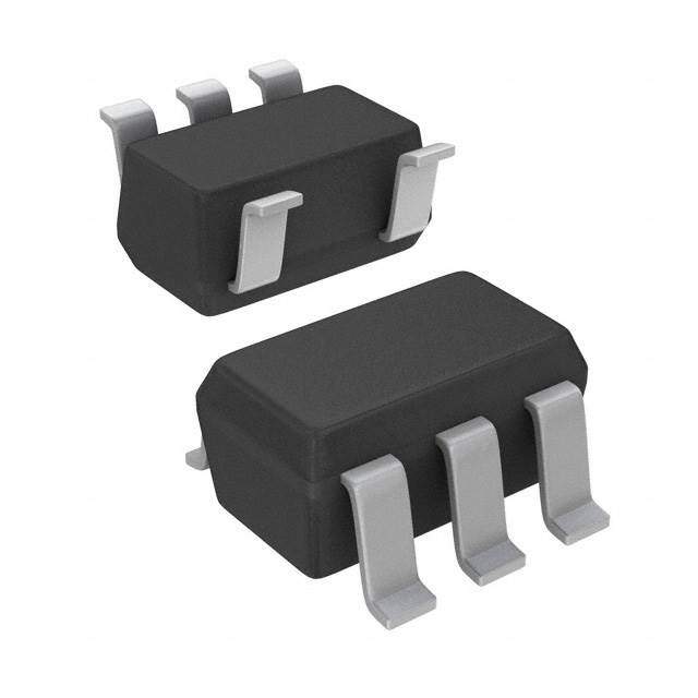
| 供应商器件封装 | SOT-23-5 |
| 其它名称 | 296-12380-1 |
| 包装 | 剪切带 (CT) |
| 单位重量 | 13 mg |
| 商标 | Texas Instruments |
| 回动电压—最大值 | 300 mV |
| 安装类型 | 表面贴装 |
| 安装风格 | SMD/SMT |
| 封装 | Reel |
| 封装/外壳 | SC-74A,SOT-753 |
| 封装/箱体 | SOT-5 |
| 工作温度 | -40°C ~ 85°C |
| 工厂包装数量 | 3000 |
| 最大功率耗散 | 0.555 W |
| 最大工作温度 | + 85 C |
| 最大输入电压 | 10 V |
| 最小工作温度 | - 40 C |
| 最小输入电压 | + 2.7 V |
| 标准包装 | 1 |
| 电压-跌落(典型值) | 0.15V @ 150mA |
| 电压-输入 | 最高 10V |
| 电压-输出 | 3.3V |
| 电压调节准确度 | 3 % |
| 电流-输出 | 150mA |
| 电流-限制(最小值) | - |
| 稳压器拓扑 | 正,固定式 |
| 稳压器数 | 1 |
| 系列 | TPS78833 |
| 线路调整率 | 0.04 % / V |
| 负载调节 | 12 mV |
| 输入偏压电流—最大 | 0.017 mA |
| 输出电压 | 3.3 V |
| 输出电流 | 150 mA |
| 输出端数量 | 1 Output |
| 输出类型 | Fixed |
| 配用 | /product-detail/zh/TPS78833EVM/296-13592-ND/486550/product-detail/zh/DEM-SOT23LDO/296-20843-ND/1216448 |


- 商务部:美国ITC正式对集成电路等产品启动337调查
- 曝三星4nm工艺存在良率问题 高通将骁龙8 Gen1或转产台积电
- 太阳诱电将投资9.5亿元在常州建新厂生产MLCC 预计2023年完工
- 英特尔发布欧洲新工厂建设计划 深化IDM 2.0 战略
- 台积电先进制程称霸业界 有大客户加持明年业绩稳了
- 达到5530亿美元!SIA预计今年全球半导体销售额将创下新高
- 英特尔拟将自动驾驶子公司Mobileye上市 估值或超500亿美元
- 三星加码芯片和SET,合并消费电子和移动部门,撤换高东真等 CEO
- 三星电子宣布重大人事变动 还合并消费电子和移动部门
- 海关总署:前11个月进口集成电路产品价值2.52万亿元 增长14.8%


PDF Datasheet 数据手册内容提取
TPS78825, TPS78833 SLVS382A – JUNE 2001 – REVISED JULY 2001 150-mA LOW-NOISE LDO WITH IN-RUSH CURRENT CONTROL FOR USB APPLICATION FEATURES DESCRIPTION (cid:1) 150-mA Low-Dropout Regulator The TPS78825 and TPS78833 are very small (SOT-23) (cid:1) Available in 2.5 V, 3.3 V package, low-noise LDOs that regulate the output (cid:1) Programmable Slew Rate Control voltage to 2.5 V and 3.3 V with input voltage ranging (cid:1) Output Noise Typically 56 µV from 2.7 V to an absolute maximum of 13.5V. These RMS (cid:1) Only 17 µA Quiescent Current at 150 mA devices output 150 mA with a peak current of 350mA (typ). The TPS788xx family uses the SR pin to program (cid:1) 1 µA Quiescent Current in Standby Mode the output voltage slew rate to control the in-rush (cid:1) Dropout Voltage Typically 150 mV at 150 mA current. This is specifically used in the USB application (TPS78833) where large load capacitance is present at start-up. The (cid:1) Over Current Limitation TPS788xx devices use only 17µA of quiescent current (cid:1) –40°C to 125°C Operating Junction and exhibit only 56 µVRMS of output voltage noise using a 10 µF output capacitor. Temperature Range (cid:1) 5-Pin SOT-23 (DBV) Package The usual PNP pass transistor has been replaced by a PMOS pass element. Because the PMOS pass element DBV PACKAGE behaves as a low-value resistor, the dropout voltage is (TOP VIEW) very low, typically 150 mV at 150 mA of load current, and is directly proportional to the load current. IN 1 5 OUT The TPS788xx also features a logic-enabled sleep GND 2 mode to shut down the regulator, reducing quiescent current to 1 µA typical at T = 25°C. J EN 3 4 SR QUIESCENT CURRENT OUTPUT VOLTAGE, ENABLE VOLTAGE vs vs FREE-AIR TEMPERATURE TIME (START-UP) 25 V VCC = 4.3 V e – IO = 150 mA ag 5 A 20 Volt µurrent – 15 IO = 1 mA Enable 0 C(SR) = 0.01 µF Quiescent C 105 put Voltage – V 312 C(SR) = 0.1 µF VVIOIO == = 41 3.53.03 V mVA ut 0 Co = 10 µF 0–40–25–105 20 35 50 65 80 95 110125 V – OO 0 10 20 30 40 50 60TJ =7 0258°C0 90 100 TA – Free-Air Temperature – °C t – Time – ms Please be aware that an important notice concerning availability, standard warranty, and use in critical applications of TexasInstruments semiconductor products and disclaimers thereto appears at the end of this data sheet. PRODUCTION DATA information is current as of publication date. Copyright 2001, Texas Instruments Incorporated Products conform to specifications per the terms of Texas Instruments standard warranty. Production processing does not necessarily include testing of all parameters. www.ti.com 1
TPS78825, TPS78833 SLVS382A – JUNE 2001 – REVISED JULY 2001 AVAILABLE OPTIONS TJ VOLTAGE PACKAGE PART NUMBER SYMBOL 2.5 V SSOOTT-2233 TPS78825DBVT† TPS78825DBVR‡ PGZI –4400°°CC ttoo 112255°°CC 3.3 V (DBV) TPS78833DBVT TPS78833DBVR PGTI †The DBVT indicates tape and reel of 250 parts. ‡The DBVR indicates tape and reel of 3000 parts. functional block diagram IN OUT EN 150 k Current Limit / Thermal Vref Protection GND SR Terminal Functions TERMINAL II//OO DDEESSCCRRIIPPTTIIOONN NAME NO. EN 3 I Active low enable GND 2 Regulator ground IN 1 I The IN terminal is the input to the device. OUT 5 O The OUT terminal is the regulated output of the device. SR 4 I The SR terminal is used to control the in-rush current. absolute maximum ratings over operating free-air temperature range (unless otherwise noted)§ Input voltage range (cid:2)(cid:3)(cid:4)(cid:4) (cid:5)(cid:6)(cid:7)(cid:4) (cid:8)(cid:9) . . . . . . . . . . . . . . . . . . . . . . . . . . . . . . . . . . . . . . . . . . . . . . . . . . . . . . . . –0.3 V to 13.5 V Voltage range at EN . . . . . . . . . . . . . . . . . . . . . . . . . . . . . . . . . . . . . . . . . . . . . . . . . . . . . . . . . . . . . . . . –0.3 V to V + 0.3 V I Voltage on OUT . . . . . . . . . . . . . . . . . . . . . . . . . . . . . . . . . . . . . . . . . . . . . . . . . . . . . . . . . . . . . . . . . . . . . . . . . . . . . . . . . . 7 V Peak output current. . . . . . . . . . . . . . . . . . . . . . . . . . . . . . . . . . . . . . . . . . . . . . . . . . . . . . . . . . . . . . . . . . . . Internally limited ESD rating, HBM . . . . . . . . . . . . . . . . . . . . . . . . . . . . . . . . . . . . . . . . . . . . . . . . . . . . . . . . . . . . . . . . . . . . . . . . . . . . . . . . 2 kV Continuous total power dissipation . . . . . . . . . . . . . . . . . . . . . . . . . . . . . . . . . . . . . . . . . . See Dissipation Rating Table Operating virtual junction temperature range, T . . . . . . . . . . . . . . . . . . . . . . . . . . . . . . . . . . . . . . . . . . . –40°C to 150°C J Operating ambient temperature range, T . . . . . . . . . . . . . . . . . . . . . . . . . . . . . . . . . . . . . . . . . . . . . . . . . –40°C to 85°C A Storage temperature range, T . . . . . . . . . . . . . . . . . . . . . . . . . . . . . . . . . . . . . . . . . . . . . . . . . . . . . . . . –65°C to 150°C stg §Stresses beyond those listed under “absolute maximum ratings” may cause permanent damage to the device. These are stress ratings only, and functional operation of the device at these or any other conditions beyond those indicated under “recommended operating conditions” is not implied. Exposure to absolute-maximum-rated conditions for extended periods may affect device reliability. NOTE 1: All voltage values are with respect to network ground terminal. DISSIPATION RATING TABLE DERATING FACTOR TA ≤ 25°C TA = 70°C TA = 85°C BOARD PACKAGE RθJC RθJA ABOVE TA = 25°C POWER RATING POWER RATING POWER RATING Low K¶ DBV 65.8°C/W 259°C/W 3.9 mW/°C 386 mW 212 mW 154 mW High K# DBV 65.8°C/W 180°C/W 5.6 mW/°C 555 mW 305 mW 222 mW ¶The JEDEC Low K (1s) board design used to derive this data was a 3 inch x 3 inch, two layer board with 2 ounce copper traces on top of the board. #The JEDEC High K (2s2p) board design used to derive this data was a 3 inch x 3 inch, multilayer board with 1 ounce internal power and ground planes and 2 ounce copper traces on top and bottom of the board. 2 www.ti.com
TPS78825, TPS78833 SLVS382A – JUNE 2001 – REVISED JULY 2001 electrical characteristics over recommended operating free-air temperature range EN = 0 , TJ = –40 to 125 °C, VI = VO(typ) + 1 V, IO = 1 mA, Co = 4.7 µF, C(SR) = 0.01 µF (unless otherwise noted) PARAMETER TEST CONDITIONS MIN TYP MAX UNIT VI Input voltage (see Note 2) 2.7 10 V IO Continuous output current (see Note 3) 0 150 mA TJ Operating junction temperature –40 125 °C TJ = 25°C 2.5 TTPPSS7788882255 10 µA< IO < 150 mA, 3.5 V < VI < 10 V 2.425 2.575 OOuuttppuutt vvoollttaaggee VV TJ = 25°C 3.3 TTPPSS7788883333 10 µA< IO < 150 mA, 3.8 V < VI < 10 V 3.201 3.399 QQuuiieesscceenntt ccuurrrreenntt ((GGNNDD ccuurrrreenntt)) 10 µA< IO < 450 mA, TJ = 25°C 17 µµAA 10 µA< IO < 150 mA 28 Load regulation 10 µA< IO < 200 mA, TJ = 25°C 12 mV OOuuttpuutt vvoollttaaggee lliinnee rreegguullaattiioonn ((∆∆VVOO//VVOO)) VO + 1 V < VI ≤ 10 V, TJ = 25°C 0.04 %%//VV (see Note 5) VO + 1 V < VI ≤ 10 V 0.1 BW = 200 Hz to 100 kHz, IO = 150 mA, Output noise voltage (TPS78833) TJ = 25°C, 56 µVRMS Co = 10 µF, C(SR) = 0.47 µF RRLL == 2222 ΩΩ,, C(byp) = 0.01 µF 10 TTiimmee,, ssttaarrtt-uup ((TTPPSS7788883333)) CCoo == 1100 µµFF,, C(byp) = 0.1 µF 50 mmss TJ = 25°C C(byp) = 0.47 µF 300 VO = 0 V (see Note 4) Output current limit 350 750 mA Standby current EN = 0 V, 2.7 V < VI < 10 V 1 2 µA High level enable input voltage 2.7 V < VI < 10 V 1.7 V Low level enable input voltage 2.7 V < VI < 10 V 0.9 V Input current (EN) EN = 0 –1 1 µA f = 1 kHz, C(SL) = 0.01 µF, Power supply ripple rejection TPS78833 TJ = 25°C, IO = 150 mA, 70 dB Co = 10 µF IO = 150 mA, TJ = 25°C 150 DDrrooppoouutt vvoollttaaggee ((sseeee NNoottee 66)) TTPPSS7788883333 mmVV IO = 150 mA 300 NOTES: 2. To calculate the minimum input voltage for your maximum output current, use the following formula: VI(min) = VO(max) + VDO (max load) 3. Continuous output current and operating junction temperature are limited by internal protection circuitry, but it is not recommended that the device operate under conditions beyond those specified in this table for extended periods of time. 4. The minimum IN operating voltage is 2.7 V or VO(typ) + 1 V, whichever is greater. The maximum IN voltage is 5.5 V. The maximum output current is 200 mA. 5. If VO≤ 2.5 V then VImin = 2.7 V, VImax = 5.5 V: (cid:2) (cid:4) V V (cid:6)2.7V Lineregulation(mV) (cid:1) (cid:2)%(cid:3)V(cid:4) (cid:5) O Imax (cid:5)1000 100 If VO > 2.5 V then VImin = VO + 1 V, VImax = 5.5 V. 6. IN voltage equals VO(typ) – 100 mV www.ti.com 3
TPS78825, TPS78833 SLVS382A – JUNE 2001 – REVISED JULY 2001 TYPICAL CHARACTERISTICS OUTPUT VOLTAGE OUTPUT VOLTAGE QUIESCENT CURRENT vs vs vs LOAD CURRENT FREE-AIR TEMPERATURE FREE-AIR TEMPERATURE 3.315 3.2 25 3.31 VTJC =C 2=5 4°C.3 V 3.33.1351 VCC = 4.3 V IO = 1 mA 20 VCC = 4.3 V IO = 150 mA A – Output Voltage – VVO33..23390.553 – Output Voltage – VVO333...33223..389022.555893 IO = 150 mA µQuiescent Current – 11055 IO = 1 mA 3.29 3.275 3.285 3.27 0 0 15 30 45 60 75 90 105120135150 –40–25–10 5 20 35 50 65 80 95 110125 –40–25–105 20 35 50 65 80 95 110125 IL – Load Current – mA TA – Free-Air Temperature – °C TA – Free-Air Temperature – °C Figure 1 Figure 2 Figure 3 OUTPUT SPECTRAL NOISE DENSITY ROOT MEAN SQUARED OUTPUT NOISE OUTPUT IMPEDANCE vs vs vs FREQUENCY S) SLEW RATE CAPACITANCE FREQUENCY nV/Noise Density – Hz 234000000 IO = 1 mAIO = 150 mA µared Output Noise –V(RM 1068000 VVICBOWIOo = = = = = 4 1 1 3.5230.003 Vµ 0 mVFHAz to 100 kHz Ωput Impedance – 11110.....1264828 VCIo = = 4 4.3.7 V µF Output Spectral 1000100 VCCIo( S= =R 4 4). 3.=7 V 0µ1.F4 k7 µF 10 k 100 k S – Root Mean Squ 24000.001 0.01 0.1 1 – OutZo 000...024610 IO1 =0 01 mIOA = 115 k0 mA10 k 100 k 1 M f – Frequency – Hz RM C(sr) – Slew Rate Capacitance – µF f – Frequency – Hz Figure 4 Figure 5 Figure 6 DROPOUT VOLTAGE RIPPLE REJECTION OUTPUT VOLTAGE, ENABLE VOLTAGE vs vs vs FREE-AIR TEMPERATURE FREQUENCY TIME (START-UP) 200 120 V – Dropout Voltage – VVDO 11055000 VCICO == 31.520 V mA Ripple Rejection – dB 110987654100000000 VVCCIOo( S= ==R 4 1)3. 30=.I3 OVµ0 VF .=4 71 5µ0F mA IO = 1 mA put Voltage – VEnable Voltage – 03152 VVICOIO( S== =R 41 )3.5 3=.03 V 0 mV.4A7 µF IO = 1 mA 30 – Out 0 CTJo == 2150° CµF 0 20 O –40–25–105 20 35 50 65 80 95 110125 10 100 1 k 10 k 100 k 1 M V 0 100200300400 5006007008009001000 TA – Free-Air Temperature – °C f – Frequency – Hz t – Time – ms Figure 7 Figure 8 Figure 9 4 www.ti.com
TPS78825, TPS78833 SLVS382A – JUNE 2001 – REVISED JULY 2001 TYPICAL CHARACTERISTICS OUTPUT VOLTAGE, ENABLE VOLTAGE vs TIME (START-UP) V LINE TRANSIENT RESPONSE A LOAD TRANSIENT RESPONSE Enable Voltage – V 05 C(SR) = 0.01 µF V– Input Voltage – I 200 VCOo == 130.3 µ VF ddvt = 0.µ2s V – Output Current – m 1200000 ddIt =0.0µ7s5 A V – Output Voltage – VO 31020 C10(SR2)0 = 03.01 µ4F0 50 60VVICTOJIOo = ==7 == 04 12 13.5530.80°3 VCµ0 mVFA90 100 – Output Voltage – mVO–542..0330 20 40 60 80 100120 140160180200 ∆ – Change InVOOutput Voltage – mVIO–1–05500000 20 40 60 80 100120VVC1IOo 4= 0== 4 131.30.63 0Vµ VF180200 t – Time – ms V t – Time – µs t – Time – µs Figure 10 Figure 11 Figure 12 TYPICAL REGIONS OF STABILITY TYPICAL REGIONS OF STABILITY EQUIVALENT SERIES RESISTANCE (ESR) EQUIVALENT SERIES RESISTANCE (ESR) vs vs OUTPUT CURRENT OUTPUT CURRENT 100 100 ΩESR – Equivalent Series Resistance – 101 RReeggioionn o of fS ItnasbVVCtialiIOobt y= i =l= it4 y43.3..73 V µVF ΩESR – Equivalent Series Resistance – 101 RegRioeng oiof nIn osft aSbtialibtyiliVVCtyIOo = == 4 13.30.3 Vµ VF 0.1 0.1 0 60 90 120 150 0 60 90 120 150 IO – Output Current – mA IO – Output Current – mA Figure 13 Figure 14 www.ti.com 5
TPS78825, TPS78833 SLVS382A – JUNE 2001 – REVISED JULY 2001 APPLICATION INFORMATION The TPS788xx family of low-dropout (LDO) regulators has been optimized for use in battery-operated equipment. It features extremely low dropout voltages, low output noise, low quiescent current (17 µA typically), and enable inputs to reduce supply currents to 1 µA when the regulator is turned off. A typical application circuit is shown in Figure 15. 1 VI IN 4 SR 5 OUT VO 1 µF 3 0.01 µF EN + 4.7 µF GND 2 ESR = 0.2 Ω Figure 15. Typical Application Circuit external capacitor requirements Although not required, a 0.047-µF or larger ceramic input bypass capacitor, connected between IN and GND and located close to the TPS788xx, is recommended to improve transient response and noise rejection. A higher-value electrolytic input capacitor may be necessary if large, fast-rise-time load transients are anticipated and the device is located several inches from the power source. Like all low dropout regulators, the TPS788xx requires an output capacitor connected between OUT and GND to stabilize the internal control loop. The minimum recommended capacitance is 4.7 µF. The ESR (equivalent series resistance) of the capacitor should be between 0.2 Ω and 10 Ω. to ensure stability. Capacitor values larger than 4.7 µF are acceptable, and allow the use of smaller ESR values. Capacitances less than 4.7 µF are not recommended because they require careful selection of ESR to ensure stability. Solid tantalum electrolytic, aluminum electrolytic, and multilayer ceramic capacitors are all suitable, provided they meet the requirements described above. Most of the commercially available 4.7 µF surface-mount solid tantalum capacitors, including devices from Sprague, Kemet, and Nichico, meet the ESR requirements stated above. Multilayer ceramic capacitors may have very small equivalent series resistances and may thus require the addition of a low value series resistor to ensure stability. CAPACITOR SELECTION PART NO. MFR. VALUE MAX ESR† SIZE (H × L × W)† T494B475K016AS Kemet 4.7 µF 1.5 Ω 1.9 × 3.5 × 2.8 195D106x0016x2T Sprague 10 µF 1.5 Ω 1.3 × 7.0 × 2.7 695D106x003562T Sprague 10 µF 1.3 Ω 2.5 × 7.6 × 2.5 TPSC475K035R0600 AVX 4.7 µF 0.6 Ω 2.6 × 6.0 × 3.2 †Size is in mm. The ESR maximum resistance is in Ohms at 100 kHz and TA = 25°C. Contact the manufacturer for the minimum ESR values. 6 www.ti.com
TPS78825, TPS78833 SLVS382A – JUNE 2001 – REVISED JULY 2001 APPLICATION INFORMATION external capacitor requirements (continued) The external bypass capacitor, used in conjunction with an internal resistor to form a low-pass filter, should be a low ESR ceramic capacitor. For example, the TPS78833 exhibits only 56 µV of output voltage noise using RMS a 0.01 µF ceramic bypass capacitor and a 10-µF ceramic output capacitor. Note that the output will start up slower as the bypass capacitance increases due to the RC time constant at the bypass pin that is created by the internal 150-kΩ resistor and external capacitor. power dissipation and junction temperature Specified regulator operation is assured to a junction temperature of 125°C; the maximum junction temperature should be restricted to 125°C under normal operating conditions. This restriction limits the power dissipation the regulator can handle in any given application. To ensure the junction temperature is within acceptable limits, calculate the maximum allowable dissipation, P , and the actual dissipation, P , which must be less than D(max) D or equal to P . D(max) The maximum-power-dissipation limit is determined using the following equation: T max(cid:6)T P (cid:1) J A D(max) RθJA Where: TJmax is the maximum allowable junction temperature. RθJA is the thermal resistance junction-to-ambient for the package, see the dissipation rating table. TA is the ambient temperature. The regulator dissipation is calculated using: (cid:2) (cid:4) P (cid:1) V (cid:6)V (cid:5)I D I O O Power dissipation resulting from quiescent current is negligible. Excessive power dissipation will trigger the thermal protection circuit. regulator protection The TPS788xx PMOS-pass transistor has a built-in back diode that conducts reverse current when the input voltage drops below the output voltage (e.g., during power down). Current is conducted from the output to the input and is not internally limited. If extended reverse voltage operation is anticipated, external limiting might be appropriate. The TPS788xx features internal current limiting and thermal protection. During normal operation, the TPS78833 limits output current to approximately 350 mA. When current limiting engages, the output voltage scales back linearly until the overcurrent condition ends. While current limiting is designed to prevent gross device failure, care should be taken not to exceed the power dissipation ratings of the package. If the temperature of the device exceeds approximately 165°C, thermal-protection circuitry shuts it down. Once the device has cooled down to below approximately 140°C, regulator operation resumes. www.ti.com 7
PACKAGE OPTION ADDENDUM www.ti.com 6-Feb-2020 PACKAGING INFORMATION Orderable Device Status Package Type Package Pins Package Eco Plan Lead/Ball Finish MSL Peak Temp Op Temp (°C) Device Marking Samples (1) Drawing Qty (2) (6) (3) (4/5) TPS78825DBVR ACTIVE SOT-23 DBV 5 3000 Green (RoHS NIPDAU Level-1-260C-UNLIM 0 to 70 PGZI & no Sb/Br) TPS78825DBVT ACTIVE SOT-23 DBV 5 250 Green (RoHS NIPDAU Level-1-260C-UNLIM 0 to 70 PGZI & no Sb/Br) TPS78833DBVR ACTIVE SOT-23 DBV 5 3000 Green (RoHS NIPDAU Level-1-260C-UNLIM 0 to 70 PGTI & no Sb/Br) TPS78833DBVT ACTIVE SOT-23 DBV 5 250 Green (RoHS NIPDAU Level-1-260C-UNLIM 0 to 70 PGTI & no Sb/Br) (1) The marketing status values are defined as follows: ACTIVE: Product device recommended for new designs. LIFEBUY: TI has announced that the device will be discontinued, and a lifetime-buy period is in effect. NRND: Not recommended for new designs. Device is in production to support existing customers, but TI does not recommend using this part in a new design. PREVIEW: Device has been announced but is not in production. Samples may or may not be available. OBSOLETE: TI has discontinued the production of the device. (2) RoHS: TI defines "RoHS" to mean semiconductor products that are compliant with the current EU RoHS requirements for all 10 RoHS substances, including the requirement that RoHS substance do not exceed 0.1% by weight in homogeneous materials. Where designed to be soldered at high temperatures, "RoHS" products are suitable for use in specified lead-free processes. TI may reference these types of products as "Pb-Free". RoHS Exempt: TI defines "RoHS Exempt" to mean products that contain lead but are compliant with EU RoHS pursuant to a specific EU RoHS exemption. Green: TI defines "Green" to mean the content of Chlorine (Cl) and Bromine (Br) based flame retardants meet JS709B low halogen requirements of <=1000ppm threshold. Antimony trioxide based flame retardants must also meet the <=1000ppm threshold requirement. (3) MSL, Peak Temp. - The Moisture Sensitivity Level rating according to the JEDEC industry standard classifications, and peak solder temperature. (4) There may be additional marking, which relates to the logo, the lot trace code information, or the environmental category on the device. (5) Multiple Device Markings will be inside parentheses. Only one Device Marking contained in parentheses and separated by a "~" will appear on a device. If a line is indented then it is a continuation of the previous line and the two combined represent the entire Device Marking for that device. (6) Lead/Ball Finish - Orderable Devices may have multiple material finish options. Finish options are separated by a vertical ruled line. Lead/Ball Finish values may wrap to two lines if the finish value exceeds the maximum column width. Important Information and Disclaimer:The information provided on this page represents TI's knowledge and belief as of the date that it is provided. TI bases its knowledge and belief on information provided by third parties, and makes no representation or warranty as to the accuracy of such information. Efforts are underway to better integrate information from third parties. TI has taken and Addendum-Page 1
PACKAGE OPTION ADDENDUM www.ti.com 6-Feb-2020 continues to take reasonable steps to provide representative and accurate information but may not have conducted destructive testing or chemical analysis on incoming materials and chemicals. TI and TI suppliers consider certain information to be proprietary, and thus CAS numbers and other limited information may not be available for release. In no event shall TI's liability arising out of such information exceed the total purchase price of the TI part(s) at issue in this document sold by TI to Customer on an annual basis. Addendum-Page 2
PACKAGE MATERIALS INFORMATION www.ti.com 28-Jan-2017 TAPE AND REEL INFORMATION *Alldimensionsarenominal Device Package Package Pins SPQ Reel Reel A0 B0 K0 P1 W Pin1 Type Drawing Diameter Width (mm) (mm) (mm) (mm) (mm) Quadrant (mm) W1(mm) TPS78825DBVR SOT-23 DBV 5 3000 180.0 9.0 3.15 3.2 1.4 4.0 8.0 Q3 TPS78825DBVT SOT-23 DBV 5 250 180.0 9.0 3.15 3.2 1.4 4.0 8.0 Q3 TPS78833DBVR SOT-23 DBV 5 3000 180.0 8.4 3.2 3.2 1.4 4.0 8.0 Q3 TPS78833DBVT SOT-23 DBV 5 250 180.0 8.4 3.2 3.2 1.4 4.0 8.0 Q3 PackMaterials-Page1
PACKAGE MATERIALS INFORMATION www.ti.com 28-Jan-2017 *Alldimensionsarenominal Device PackageType PackageDrawing Pins SPQ Length(mm) Width(mm) Height(mm) TPS78825DBVR SOT-23 DBV 5 3000 182.0 182.0 20.0 TPS78825DBVT SOT-23 DBV 5 250 182.0 182.0 20.0 TPS78833DBVR SOT-23 DBV 5 3000 210.0 185.0 35.0 TPS78833DBVT SOT-23 DBV 5 250 210.0 185.0 35.0 PackMaterials-Page2
IMPORTANTNOTICEANDDISCLAIMER TI PROVIDES TECHNICAL AND RELIABILITY DATA (INCLUDING DATASHEETS), DESIGN RESOURCES (INCLUDING REFERENCE DESIGNS), APPLICATION OR OTHER DESIGN ADVICE, WEB TOOLS, SAFETY INFORMATION, AND OTHER RESOURCES “AS IS” AND WITH ALL FAULTS, AND DISCLAIMS ALL WARRANTIES, EXPRESS AND IMPLIED, INCLUDING WITHOUT LIMITATION ANY IMPLIED WARRANTIES OF MERCHANTABILITY, FITNESS FOR A PARTICULAR PURPOSE OR NON-INFRINGEMENT OF THIRD PARTY INTELLECTUAL PROPERTY RIGHTS. These resources are intended for skilled developers designing with TI products. You are solely responsible for (1) selecting the appropriate TI products for your application, (2) designing, validating and testing your application, and (3) ensuring your application meets applicable standards, and any other safety, security, or other requirements. These resources are subject to change without notice. TI grants you permission to use these resources only for development of an application that uses the TI products described in the resource. Other reproduction and display of these resources is prohibited. No license is granted to any other TI intellectual property right or to any third party intellectual property right. TI disclaims responsibility for, and you will fully indemnify TI and its representatives against, any claims, damages, costs, losses, and liabilities arising out of your use of these resources. TI’s products are provided subject to TI’s Terms of Sale (www.ti.com/legal/termsofsale.html) or other applicable terms available either on ti.com or provided in conjunction with such TI products. TI’s provision of these resources does not expand or otherwise alter TI’s applicable warranties or warranty disclaimers for TI products. Mailing Address: Texas Instruments, Post Office Box 655303, Dallas, Texas 75265 Copyright © 2020, Texas Instruments Incorporated