ICGOO在线商城 > 集成电路(IC) > PMIC - 稳压器 - 线性 > TPS78330DDCT
 Datasheet下载
- 型号: TPS78330DDCT
- 制造商: Texas Instruments
- 库位|库存: xxxx|xxxx
- 要求:
| 数量阶梯 | 香港交货 | 国内含税 |
| +xxxx | $xxxx | ¥xxxx |
查看当月历史价格
查看今年历史价格
TPS78330DDCT产品简介:
ICGOO电子元器件商城为您提供TPS78330DDCT由Texas Instruments设计生产,在icgoo商城现货销售,并且可以通过原厂、代理商等渠道进行代购。 TPS78330DDCT价格参考。Texas InstrumentsTPS78330DDCT封装/规格:PMIC - 稳压器 - 线性, Linear Voltage Regulator IC Positive Fixed 1 Output 3V 150mA SOT-23-5。您可以下载TPS78330DDCT参考资料、Datasheet数据手册功能说明书,资料中有TPS78330DDCT 详细功能的应用电路图电压和使用方法及教程。
TPS78330DDCT 是 Texas Instruments(德州仪器)推出的一款低功耗、低压差线性稳压器(LDO),属于 PMIC - 稳压器 - 线性分类。它具有 3.0V 的固定输出电压,适用于多种需要高效能和低噪声电源管理的应用场景。以下是其主要应用场景:

1. 便携式设备
   TPS78330DDCT 因其低静态电流(典型值为 950nA)和小封装尺寸(DDC 封装),非常适合用于电池供电的便携式设备,如智能手机、平板电脑、可穿戴设备(智能手表、健康监测器)等。这些设备对功耗和空间要求较高,而该器件能够提供高效的电源管理。

2. 物联网(IoT)设备
   在 IoT 领域,TPS78330DDCT 可为传感器节点、无线模块(如蓝牙、Wi-Fi 模块)和其他低功耗设备供电。其低功耗特性有助于延长电池寿命,同时支持稳定的电压输出以确保设备正常运行。

3. 工业自动化与控制
   该器件可用于工业环境中需要稳定电源供应的场合,例如数据采集系统、远程监控设备、传感器接口等。其高精度输出电压和良好的负载/线路调节能力,使其适合对电源质量要求较高的工业应用。

4. 消费电子
   TPS78330DDCT 可广泛应用于消费电子产品,如数码相机、便携式音频播放器、电子阅读器等。这些设备通常需要一个稳定的电源来驱动微控制器、存储器和其他外围组件。

5. 通信设备
   在通信领域,该器件可用于基站中的低功耗子系统、路由器、调制解调器等。其低噪声性能有助于提高射频(RF)电路的信号完整性。

6. 汽车电子(非关键安全区域)
   虽然 TPS78330DDCT 不是专门设计用于汽车 AEC-Q100 标准的产品,但在一些非关键安全区域(如信息娱乐系统、遥控钥匙模块等),它仍然可以作为辅助电源解决方案使用。

总结来说,TPS78330DDCT 凭借其低功耗、小尺寸和高稳定性,特别适合于需要长时间运行且对电源效率敏感的应用场景,涵盖从消费电子到工业自动化等多个领域。
| 参数 | 数值 |
| 产品目录 | 集成电路 (IC)半导体 |
| 描述 | IC REG LDO 3V 0.15A 5SOT低压差稳压器 150mA Ultra-Lo Quies Crnt Iq0.5uA LDO Reg |
| 产品分类 | |
| 品牌 | Texas Instruments |
| 产品手册 | |
| 产品图片 |
|
| rohs | 符合RoHS无铅 / 符合限制有害物质指令(RoHS)规范要求 |
| 产品系列 | 电源管理 IC,低压差稳压器,Texas Instruments TPS78330DDCT- |
| 数据手册 | |
| 产品型号 | TPS78330DDCT |
| PSRR/纹波抑制—典型值 | 40 dB at 10 Hz |
| 产品种类 | 低压差稳压器 |
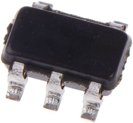
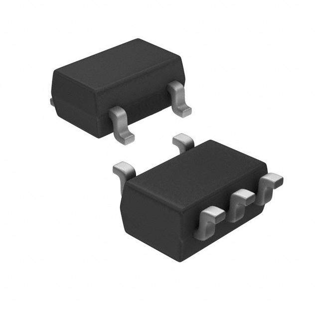
| 供应商器件封装 | 5-SOT |
| 其它名称 | 296-27178-1 |
| 包装 | 剪切带 (CT) |
| 商标 | Texas Instruments |
| 回动电压—最大值 | 250 mV |
| 安装类型 | 表面贴装 |
| 安装风格 | SMD/SMT |
| 封装 | Reel |
| 封装/外壳 | SOT-23-5 细型,TSOT-23-5 |
| 封装/箱体 | SOT-23-5 |
| 工作温度 | -40°C ~ 105°C |
| 工厂包装数量 | 250 |
| 最大工作温度 | + 105 C |
| 最大输入电压 | 5.5 V |
| 最小工作温度 | - 40 C |
| 最小输入电压 | 2.2 V |
| 标准包装 | 1 |
| 电压-跌落(典型值) | 0.13V @ 150mA |
| 电压-输入 | 最高 5.5V |
| 电压-输出 | 3V |
| 电压调节准确度 | 2 % |
| 电流-输出 | 150mA |
| 电流-限制(最小值) | 150mA |
| 稳压器拓扑 | 正,固定式 |
| 稳压器数 | 1 |
| 系列 | TPS78330 |
| 线路调整率 | 1 % |
| 负载调节 | 1 % |
| 输出电压 | 3 V |
| 输出电流 | 150 mA |
| 输出端数量 | 1 Output |
| 输出类型 | Fixed |


- 商务部:美国ITC正式对集成电路等产品启动337调查
- 曝三星4nm工艺存在良率问题 高通将骁龙8 Gen1或转产台积电
- 太阳诱电将投资9.5亿元在常州建新厂生产MLCC 预计2023年完工
- 英特尔发布欧洲新工厂建设计划 深化IDM 2.0 战略
- 台积电先进制程称霸业界 有大客户加持明年业绩稳了
- 达到5530亿美元!SIA预计今年全球半导体销售额将创下新高
- 英特尔拟将自动驾驶子公司Mobileye上市 估值或超500亿美元
- 三星加码芯片和SET,合并消费电子和移动部门,撤换高东真等 CEO
- 三星电子宣布重大人事变动 还合并消费电子和移动部门
- 海关总署:前11个月进口集成电路产品价值2.52万亿元 增长14.8%


PDF Datasheet 数据手册内容提取
Product Sample & Technical Tools & Support & Folder Buy Documents Software Community TPS783 SBVS133A–FEBRUARY2010–REVISEDNOVEMBER2014 TPS783xx 500-nA I , 150-mA, Ultralow Quiescent Current Q Low-Dropout Linear Regulator 1 Features 3 Description • InputVoltageRange:2.2Vto5.5V The TPS783 family of low-dropout regulators (LDOs) 1 offers the benefits of ultralow power and miniaturized • LowQuiescentCurrent(I ):500nA Q packaging. • 150-mA,Low-DropoutRegulator This LDO family is designed specifically for battery- • Low-Dropoutat25°C,130mVat150mA powered applications where ultralow quiescent • Low-Dropoutat85°C,175mVat150mA current is a critical parameter. The TPS783, with • 3%AccuracyOverLoad,Line,andTemperature ultralow IQ (500 nA), is ideal for microprocessors, microcontrollers, and other battery-powered • Stablewitha1.0-μFCeramicCapacitor applications. • ThermalShutdownandOvercurrentProtection The absence of pulldown circuitry at the output of the • CMOSLogicLevel-CompatibleEnablePin LDOprovidestheflexibilitytousetheregulatoroutput • DDC(SOT-5)Package capacitor as a temporary backup power supply (for example,duringbatteryreplacement). 2 Applications The ultralow power and miniaturized packaging allow • TIMSP430AttachApplications designers to customize power consumption for • WirelessHandsetsandSmartphones specific applications. Consult with your local factory representative for exact voltage options and ordering • MP3Players information;minimumorderquantitiesmayapply. • Battery-OperatedHandheldProducts The TPS783 family is compatible with the TI MSP430 and other similar products. The enable pin (EN) is compatible with standard CMOS logic. This device allows for minimal board space because of miniaturized packaging and a potentially small output capacitor. The TPS783 family also features thermal shutdown and current limit to protect the device during fault conditions. All packages have a specified operatingtemperaturerangeofT =–40°Cto105°C. J DeviceInformation(1) PARTNUMBER PACKAGE BODYSIZE(NOM) TPS783xx SOT(5) 2.90mm×1.60mm (1) Forallavailablepackages,seethepackageoptionaddendum attheendofthedatasheet. SimplifiedSchematic TPS783xxDDC SOT-5 VIN IN OUT VOUT (Top View) 1mF 2.2mF TPS783xx IN 1 5 OUT On GND 2 Off EN EN 3 4 GND GND 1 An IMPORTANT NOTICE at the end of this data sheet addresses availability, warranty, changes, use in safety-critical applications, intellectualpropertymattersandotherimportantdisclaimers.PRODUCTIONDATA.
TPS783 SBVS133A–FEBRUARY2010–REVISEDNOVEMBER2014 www.ti.com Table of Contents 1 Features.................................................................. 1 7.4 DeviceFunctionalModes........................................10 2 Applications........................................................... 1 8 ApplicationandImplementation........................ 11 3 Description............................................................. 1 8.1 ApplicationInformation............................................11 4 RevisionHistory..................................................... 2 8.2 TypicalApplication..................................................11 8.3 SystemExamples...................................................13 5 PinConfigurationandFunctions......................... 3 8.4 Do'sandDon’ts.......................................................15 6 Specifications......................................................... 4 9 Power-SupplyRecommendations...................... 15 6.1 AbsoluteMaximumRatings......................................4 10 Layout................................................................... 15 6.2 HandlingRatings.......................................................4 6.3 RecommendedOperatingConditions.......................4 10.1 LayoutGuidelines.................................................15 6.4 ThermalInformation..................................................4 10.2 LayoutExample....................................................16 6.5 ElectricalCharacteristics...........................................5 11 DeviceandDocumentationSupport................. 17 6.6 TypicalCharacteristics..............................................6 11.1 DeviceSupport ....................................................17 7 DetailedDescription.............................................. 9 11.2 Trademarks...........................................................17 7.1 Overview...................................................................9 11.3 ElectrostaticDischargeCaution............................17 7.2 FunctionalBlockDiagram.........................................9 11.4 Glossary................................................................17 7.3 FeatureDescription...................................................9 12 Mechanical,Packaging,andOrderable Information........................................................... 17 4 Revision History ChangesfromOriginal(February2010)toRevisionA Page • Changeddocumentformattolatestdatasheetstandards;addedHandlingRatings,ThermalInformation, RecommendedOperatingConditions,PowerSupplyRecommendations,andDeviceandDocumentationSupport sections;movedexistingsections.......................................................................................................................................... 1 • Deletedfactoryprogrammingfeaturebullet .......................................................................................................................... 1 • Addedinputvoltagerangefeaturebullet............................................................................................................................... 1 • Deletedprogrammablemodeapplicationbullet..................................................................................................................... 1 • Addedsimplifiedschematictofrontpage............................................................................................................................... 1 • ChangedPinFunctionstable ................................................................................................................................................ 3 • ChangedoperatingjunctiontemperaturemaximumvalueinAbsoluteMaximumRatingstable........................................... 4 • DeletedDissipationRatingstable;seeThermalInformationtable......................................................................................... 4 • ChangedsymbolandparameternamesforclarityinElectricalCharacteristicstable........................................................... 5 • Addedfootnote(2)toElectricalCharacteristicstable............................................................................................................ 5 • ChangedFigure7y-axistitleandmeasurementrange......................................................................................................... 7 • ChangedFigure9V labelstomatchElectricalCharacteristicstable................................................................................. 7 EN • ChangedFigure10y-axistitletomatchElectricalCharacteristicstable............................................................................... 7 • DeletedFigure14I condition............................................................................................................................................ 7 OUT • DeletedFigure15I condition............................................................................................................................................ 7 OUT • ChangedFunctionalBlockDiagram....................................................................................................................................... 9 • ChangedFigure18 .............................................................................................................................................................. 10 • AddedreferenceforTable1inDeviceFunctionalModes................................................................................................... 10 • ChangedFigure19............................................................................................................................................................... 11 • ChangedTable2format....................................................................................................................................................... 14 2 SubmitDocumentationFeedback Copyright©2010–2014,TexasInstrumentsIncorporated ProductFolderLinks:TPS783
TPS783 www.ti.com SBVS133A–FEBRUARY2010–REVISEDNOVEMBER2014 5 Pin Configuration and Functions DDCPackage SOT-5 (TopView) IN 1 5 OUT GND 2 EN 3 4 GND PinFunctions PIN I/O DESCRIPTION NAME NO. Enablepin.Drivethispinover1.2Vtoturnontheregulator.Drivethispinbelow0.4Vtoput EN 3 I theregulatorintoshutdownmode,reducingoperatingcurrentto18nA,typical. GND 2,4 — Groundpin.Tieallgroundpinstogroundforproperoperation. Inputpin.Forstableoperation,placeasmall,0.1-μFcapacitorfromthispintoground;typical IN 1 I inputcapacitor=1.0μF.TiebackbothinputandoutputcapacitorgroundstotheICground, withnosignificantimpedancebetweenthem. Regulatedoutputvoltagepin.Connectasmall(1-μForgreater)ceramiccapacitorfromthis OUT 5 O pintogroundforstableoperation.SeetheInputandOutputCapacitorRequirementsinthe ApplicationandImplementationsectionformoredetails. Copyright©2010–2014,TexasInstrumentsIncorporated SubmitDocumentationFeedback 3 ProductFolderLinks:TPS783
TPS783 SBVS133A–FEBRUARY2010–REVISEDNOVEMBER2014 www.ti.com 6 Specifications 6.1 Absolute Maximum Ratings AtT =–40°Cto105°C(unlessotherwisenoted).AllvoltagesarewithrespecttoGND.(1) J MIN MAX UNIT V –0.3 6.0 V IN Voltage ENpin –0.3 V +0.3 V IN V –0.3 V +0.3 V OUT IN I Internallylimited A OUT Current Outputshort-circuitduration Indefinite Temperature Operatingjunction,T –40 160 °C J (1) StressesbeyondthoselistedunderAbsoluteMaximumRatingsmaycausepermanentdamagetothedevice.Thesearestressratings only,whichdonotimplyfunctionaloperationofthedeviceattheseoranyotherconditionsbeyondthoseindicatedunderRecommended OperatingConditions.Exposuretoabsolute-maximum-ratedconditionsforextendedperiodsmayaffectdevicereliability. 6.2 Handling Ratings MIN MAX UNIT T Storagetemperaturerange –55 150 °C stg Electrostatic Humanbodymodel(HBM),perANSI/ESDA/JEDECJS-001,allpins(1) –2000 2000 V V (ESD) discharge Chargeddevicemodel(CDM),perJEDECspecificationJESD22-C101,allpins(2) –500 500 (1) JEDECdocumentJEP155statesthat500-VHBMallowssafemanufacturingwithastandardESDcontrolprocess. (2) JEDECdocumentJEP157statesthat250-VCDMallowssafemanufacturingwithastandardESDcontrolprocess. 6.3 Recommended Operating Conditions overoperatingjunctiontemperaturerange(unlessotherwisenoted) MIN NOM MAX UNIT V Inputvoltage 2.2 5.5 V IN V Outputvoltage 1.8 4.2 V OUT V Enablevoltage 0 V V EN IN I Outputcurrent 0 150 mA OUT T Junctiontemperature –40 105 °C J 6.4 Thermal Information TPS783xx THERMALMETRIC(1) DDC(SOT) UNIT 5PINS R Junction-to-ambientthermalresistance 193.0 θJA R Junction-to-case(top)thermalresistance 40.0 θJC(top) R Junction-to-boardthermalresistance 34.3 θJB °C/W ψ Junction-to-topcharacterizationparameter 0.9 JT ψ Junction-to-boardcharacterizationparameter 34.1 JB R Junction-to-case(bottom)thermalresistance N/A θJC(bot) (1) Formoreinformationabouttraditionalandnewthermalmetrics,seetheICPackageThermalMetricsapplicationreport,SPRA953. 4 SubmitDocumentationFeedback Copyright©2010–2014,TexasInstrumentsIncorporated ProductFolderLinks:TPS783
TPS783 www.ti.com SBVS133A–FEBRUARY2010–REVISEDNOVEMBER2014 6.5 Electrical Characteristics AtT =–40°Cto105°C,V =V +0.5Vor2.2V,whicheverisgreater;I =100μA,V =V ,C =1.0μF, J IN OUT(nom) OUT EN IN OUT andfixedV testconditions(unlessotherwisenoted).TypicalvaluesatT =25°C. OUT J PARAMETER TESTCONDITIONS MIN TYP MAX UNIT V Inputvoltagerange 2.2 5.5 V IN Nominal T =25°C –2% 2% J VOUT DCoutputaccuracy OverVIN,IOUT, VOUT+0.5V≤VIN≤5.5V, –3.0% ±2.0% 3.0% temperature 100μA≤I ≤150mA OUT ΔV Lineregulation V +0.5V≤V ≤5.5V ±1.0% O(ΔVI) OUT(nom) IN ΔV Loadregulation 100μA≤I ≤150mA ±1.0% O(ΔIO) OUT V Dropoutvoltage(1) V =95%V ,I =150mA 130 250 mV DO IN OUT(nom) OUT I Outputcurrentlimit V =0.90×V 150 230 400 mA LIM OUT OUT(nom) I =0mA 420 800 nA OUT I GNDpincurrent GND I =150mA 8 μA OUT I ENpincurrent V =V =5.5V 0.07 40 nA EN IN EN I ShutdowncurrentatGNDpin V ≤0.4V,V ≤V <5.5V(2) 18 150 nA SHDN(GND) EN IN(min) IN ShutdowncurrentatOUTpin V =open,V =0.4V, ISHDN(OUT) (leakage)(3) VIN =V EN 137 500 nA OUT OUT(nom) V Enablehigh-levelvoltage V =5.5V 1.2 V V EN(HI) IN IN V Enablelow-levelvoltage V =5.5V 0 0.4 V EN(LO) IN f=10Hz 40 dB V =4.3V, IN PSRR Power-supplyrejectionratio V =3.0V, f=100Hz 20 dB OUT I =150mA OUT f=1kHz 15 dB BW=100Hzto100kHz,V =2.2V, V Outputnoisevoltage IN 86 μV n V =1.2V,I =1mA RMS OUT OUT t Startuptime(4) COUT=1.0μF,VOUT=10%VOUT(nom)to 500 μs STR V =90%V OUT OUT(nom) Shutdown,temperatureincreasing 160 °C T Thermalshutdowntemperature sd Reset,temperaturedecreasing 140 °C T Operatingjunctiontemperature –40 125 °C J (1) V isnotmeasuredfordeviceswithV ≤2.3VbecauseminimumV =2.2V. DO OUT(nom) IN (2) V =(V +0.5V)or2.2V,whicheverisgreater. IN(min) OUT(nom) (3) SeeShutdownintheApplicationandImplementationsectionformoredetails. (4) TimefromV =1.2VtoV =90%(V ). EN OUT OUT(nom) Copyright©2010–2014,TexasInstrumentsIncorporated SubmitDocumentationFeedback 5 ProductFolderLinks:TPS783
TPS783 SBVS133A–FEBRUARY2010–REVISEDNOVEMBER2014 www.ti.com 6.6 Typical Characteristics AtT =–40°Cto105°C,V =V +0.5Vor2.2V,whicheverisgreater;I =100μA,V =V ,C =1μF,and J IN OUT(nom) OUT EN IN OUT C =1μF(unlessotherwisenoted). IN 1.0 3 0.8 -40°C 2 0.6 0.4 %) 0.2 +25°C +85°C %) 1 +25°C -40°C V(OUT -0.02 +105°C V(OUT 0 +105°C +85°C -0.4 -1 -0.6 -2 -0.8 -1.0 -3 3.5 3.7 3.9 4.1 4.3 4.5 4.7 4.9 5.1 5.3 5.5 3.5 3.7 3.9 4.1 4.3 4.5 4.7 4.9 5.1 5.3 5.5 V (V) V (V) IN IN I =5mA,V =3.0V I =150mA,V =3.0V OUT OUT(nom) OUT OUT(nom) Figure1.TPS78330LineRegulation Figure2.TPS78330LineRegulation 3 200 +85°C 2 mV) 150 +105°C %) 1 -40°C +25°C ) (UT V(OUT 0 +105°C +85°C -VVINO 100 -1 ( VDO 50 +25°C -2 -40°C -3 0 0 25 50 75 100 125 150 0 25 50 75 100 125 150 I (mA) I (mA) OUT OUT V =3.5V,V =3.0V V =3.0V,V =0.95×V IN OUT(nom) OUT(nom) IN OUT(nom) Figure3.TPS78330LoadRegulation Figure4.TPS78330DropoutVoltagevsOutputCurrent 250 900 800 200 700 V) +85°C m 600 ) (OUT 150 150mA 100mA nA) 500 V ( - ND 400 VIN 100 IG ( 50mA 300 DO -40°C V 200 50 +25°C 10mA 100 0 0 -40 -25 -10 5 20 35 50 65 80 95 110 125 3.8 4.0 4.2 4.4 4.6 4.8 5.0 5.2 5.45.5 TJ(°C) VIN(V) VOUT(nom)=3.0V,VIN=0.95×VOUT(nom) IOUT=0mA,VOUT(nom)=3.0V Figure5. TPS78330DropoutVoltagevs Figure6.TPS78330GroundPinCurrentvsInputVoltage JunctionTemperature 6 SubmitDocumentationFeedback Copyright©2010–2014,TexasInstrumentsIncorporated ProductFolderLinks:TPS783
TPS783 www.ti.com SBVS133A–FEBRUARY2010–REVISEDNOVEMBER2014 Typical Characteristics (continued) AtT =–40°Cto105°C,V =V +0.5Vor2.2V,whicheverisgreater;I =100μA,V =V ,C =1μF,and J IN OUT(nom) OUT EN IN OUT C =1μF(unlessotherwisenoted). IN 250 3.0 -40°C 2.7 240 2.4 +105°C 2.1 (mA)M 230 +25°C (nA)N 11..85 ILI 220 IE 1.2 +85°C 0.9 210 +85°C +105°C 0.6 0.3 -40°C +25°C 200 0 3.5 3.7 3.9 4.1 4.3 4.5 4.7 4.9 5.1 5.3 5.5 3.5 3.7 3.9 4.1 4.3 4.5 4.7 4.9 5.1 5.3 5.5 V (V) V (V) IN IN VOUT=95%VOUT(nom),VOUT(nom)=3.0V IOUT=100μA,VOUT(nom)=3.0V Figure7.TPS78330CurrentLimitvsInputVoltage Figure8.TPS78330EnablePinCurrentvsInputVoltage 1.2 250 1.1 200 1.0 V 0.9 EN(HI) A) n 150 V(V)EN 0.8 (N(OUT) +105°C 0.7 VEN(LO) ISHD 100 +85°C +25°C 0.6 50 0.5 -40°C 0.4 0 -40 -25 -10 5 20 35 50 65 80 95 110 125 1.0 1.2 1.4 1.6 1.8 2.0 2.2 2.4 2.6 2.8 3.0 TJ(°C) VOUT(V) IOUT=1mA,VOUT(nom)=3.0V VOUT=VOUT(nom)=3.0V,VEN=0.4V Figure9.TPS78330EnablePinHysteresisvs Figure10.TPS78330OutputCurrentLeakageatShutdown JunctionTemperature 100 3 )z H Ö V/ 2 m 10 nsity ( %) 1 100mA 10mA al Noise De 0.11 150mA V(OUT(NOM) 0 150mA 5mA ctr D -1 e 50mA Sp 0.01 1mA = 130mVRMS put 50mA = 134mVRMS -2 Out 150mA = 138.0mVRMS 1mA 0.001 -3 10 100 1k 10k 100k -40 -25 -10 5 20 35 50 65 80 95 110 125 Frequency (Hz) TJ(°C) C =1μF,C =2.2μF,V =3.5V,V =3.0V V =3.5V,V =3.0V IN OUT IN OUT(nom) IN OUT(nom) Figure11.TPS78330OutputSpectralNoiseDensity Figure12. TPS78330%ΔV vsJunctionTemperature O Copyright©2010–2014,TexasInstrumentsIncorporated SubmitDocumentationFeedback 7 ProductFolderLinks:TPS783
TPS783 SBVS133A–FEBRUARY2010–REVISEDNOVEMBER2014 www.ti.com Typical Characteristics (continued) AtT =–40°Cto105°C,V =V +0.5Vor2.2V,whicheverisgreater;I =100μA,V =V ,C =1μF,and J IN OUT(nom) OUT EN IN OUT C =1μF(unlessotherwisenoted). IN 80 VIN VIN= 0.0V to 5.0V dB) 70 VOUT= 3.0V o ( 1mA v) Enable COUT= 10mF Rati 60 V/di Cu Rejection 5400 50mA Voltage (1 Load Current VOUT rrent (50m ply 30 A/d Sup 20 0V iv) wer- 150mA o 10 P 0 10 100 1k 10k 100k 1M Time (20ms/div) Frequency (Hz) V =3.5V,V =3.0V,C =2.2μF IN OUT(nom) OUT Figure14.TPS78330InputVoltageRampvsOutputVoltage Figure13.TPS78330RippleRejectionvsFrequency VIN Enable V = 5.5V IN V = 3.0V OUT e (1V/div) VOUT Curren V/div) VIN ICOOUUTT== 1 1500mmFA Voltag Load Current VVIONU=T =5 .35.V0V t (50mA/div) Voltage (1 VENABLE VOUT C = 10mF OUT 0V Time (20ms/div) Time (500ms/div) Figure15.TPS78330OutputVoltagevsEnable(SlowRamp) Figure16.TPS78330InputVoltagevsDelaytoOutput V Enable v) IN edi Voltag100mV/ VOUT ( V = 5.5V IN VIOOUUTT== 0 3m.0AV to 10mA Load (10mCu COUT= 10mF Current A/drren ivt ) 0A Time (5ms/div) Figure17.TPS78330LoadTransientResponse 8 SubmitDocumentationFeedback Copyright©2010–2014,TexasInstrumentsIncorporated ProductFolderLinks:TPS783
TPS783 www.ti.com SBVS133A–FEBRUARY2010–REVISEDNOVEMBER2014 7 Detailed Description 7.1 Overview The TPS783 family of low-dropout regulators (LDOs) designed specifically for battery-powered applications where ultralow quiescent current is a critical parameter. The absence of pulldown circuitry at the output of the LDO provides the flexibility to use the regulator output capacitor as a temporary backup power supply for a short period of time (for example, during battery replacement). The TPS783 family is compatible with the TI MSP430 and other similar products. The enable pin (EN) is compatible with standard CMOS logic. This LDO family is stablewithanyoutputcapacitorgreaterthan1.0µF. 7.2 Functional Block Diagram IN OUT Current Limit Thermal Shutdown ±± ++ EPROM Mux EN Bandgap Logic GND 7.3 Feature Description 7.3.1 InternalCurrentLimit The TPS783 is internally current-limited to protect the regulator during fault conditions. During current limit, the output sources a fixed amount of current that is largely independent of output voltage. For reliable operation, do notoperatethedeviceinacurrent-limitstateforextendedperiodsoftime. The PMOS pass element in the TPS783 family has a built-in body diode that conducts current when the voltage at OUT exceeds the voltage at IN. This current is not limited, so if extended reverse voltage operation is anticipated,externallimitinguptothemaximumratedcurrentforthedevicemayberequired. Copyright©2010–2014,TexasInstrumentsIncorporated SubmitDocumentationFeedback 9 ProductFolderLinks:TPS783
TPS783 SBVS133A–FEBRUARY2010–REVISEDNOVEMBER2014 www.ti.com Feature Description (continued) 7.3.2 Shutdown The enable pin (EN) is active high and is compatible with standard and low-voltage CMOS levels. When shutdowncapabilityisnotrequired,connectENtotheINpin,asshowninFigure18. VIN IN OUT VOUT 1mF 1mF TPS783xx EN GND Figure18. CircuitShowingENTiedHighWhenShutdownCapabilityisNotRequired 7.4 Device Functional Modes Table1providesaquickcomparisonbetweenthenormal,dropout,anddisabledmodesofoperation. Table1.DeviceFunctionalModeComparison PARAMETER OPERATINGMODE V EN I T IN OUT J Normal V >V +V V >V I <I T <160°C IN OUT(nom) DO EN EN(HI) OUT LIM J Dropout V <V +V V >V I <I T <160°C IN OUT(nom) DO EN EN(HI) OUT LIM J Disabled — V <V — T >160°C EN EN(LO) J 7.4.1 NormalOperation Thedeviceregulatestothenominaloutputvoltageunderthefollowingconditions: • Theinputvoltageisgreaterthanthenominaloutputvoltageplusthedropoutvoltage(V +V ). OUT(nom) DO • The enable voltage has previously exceeded the enable rising threshold voltage (V > V ) and not yet EN EN(HI) decreasedbelowtheenablefallingthreshold. • Theoutputcurrentislessthanthecurrentlimit(I <I ). OUT LIM • Thedevicejunctiontemperatureislessthanthethermalshutdowntemperature(T <160°C). J 7.4.2 DropoutOperation If the input voltage is lower than the nominal output voltage plus the specified dropout voltage, but all other conditions are met for normal operation, the device operates in dropout mode. In this mode, the output voltage tracks the input voltage. During this mode, the transient performance of the device becomes significantly degraded because the pass device is in a triode state and no longer controls the current through the LDO. Line orloadtransientsindropoutcanresultinlargeoutput-voltagedeviations. 7.4.3 Disabled Thedeviceisdisabledunderthefollowingconditions: • The enable voltage is less than the enable falling threshold voltage (V < V ) or has not yet exceeded EN EN(LO) theenablerisingthreshold. • Thedevicejunctiontemperatureisgreaterthanthethermalshutdowntemperature(T >160°C). J 10 SubmitDocumentationFeedback Copyright©2010–2014,TexasInstrumentsIncorporated ProductFolderLinks:TPS783
TPS783 www.ti.com SBVS133A–FEBRUARY2010–REVISEDNOVEMBER2014 8 Application and Implementation NOTE Information in the following applications sections is not part of the TI component specification, and TI does not warrant its accuracy or completeness. TI’s customers are responsible for determining suitability of components for their purposes. Customers should validateandtesttheirdesignimplementationtoconfirmsystemfunctionality. 8.1 Application Information The TPS783 family of LDOs is factory-programmable to have a fixed output. Note that during startup or steady- stateconditions,donotallowtheENpinvoltagetoexceedV +0.3V. IN 8.2 Typical Application VIN IN OUT VOUT 1mF 2.2mF TPS783xx On Off EN GND Figure19. ProvidingaLow-PowerStandbyRail 8.2.1 DesignRequirements 8.2.1.1 InputandOutputCapacitorRequirements A 0.1-μF input capacitor is necessary for stable operation. Good analog design practice is to connect a 0.1-μF to 1.0-μF, low equivalent series resistance (ESR) capacitor across the input supply near the regulator. This capacitor counteracts reactive input sources and improves transient response, noise rejection, and ripple rejection. A higher-value capacitor may be necessary if large, fast rise-time load transients are anticipated, or if thedeviceisnotlocatednearthepowersource. The TPS783 family is designed to be stable with standard ceramic capacitors with values of 1.0 μF or larger at the output. X5R- and X7R-type capacitors are best because they have minimal variation in value and ESR over temperature. Maximum ESR must be less than 1.0 Ω. With tolerance and dc bias effects, the minimum capacitanceforstableoperationis1μF. Copyright©2010–2014,TexasInstrumentsIncorporated SubmitDocumentationFeedback 11 ProductFolderLinks:TPS783
TPS783 SBVS133A–FEBRUARY2010–REVISEDNOVEMBER2014 www.ti.com Typical Application (continued) 8.2.1.2 DropoutVoltage The TPS783 family uses a PMOS pass transistor to achieve low dropout. When (V – V ) is less than the IN OUT dropout voltage (V ), the PMOS pass device is the linear region of operation and the input-to-output resistance DO is the R of the PMOS pass element. V approximately scales with output current because the PMOS DS(ON) DO device behaves like a resistor in dropout. As with any linear regulator, PSRR and transient response are degraded as (V – V ) approaches dropout. This effect is shown in the Typical Characteristics section. Refer IN OUT toapplicationreportSLVA207,UnderstandingLDODropout,availablefordownloadfromwww.ti.com. 8.2.1.3 TransientResponse As with any regulator, increasing the size of the output capacitor reduces overshoot and undershoot magnitude butincreasesdurationofthetransientresponse.Formoreinformation,seeFigure17. 8.2.1.4 MinimumLoad The TPS783 family is stable with no output load. Traditional PMOS LDO regulators suffer from lower loop gain at very light output loads. The TPS783 employs an innovative, low-current circuit under very light or no-load conditions, resulting in improved output voltage regulation performance down to zero output current. See Figure17fortheloadtransientresponse. 8.2.2 DetailedDesignProcedure Selectthedesireddevicebasedontheoutputvoltage. Provide an input supply with adequate headroom to account for dropout and output current to account for the GNDpincurrent,andpowertheload.Selectinputandoutputcapacitorsbasedonapplicationneeds. 8.2.3 ApplicationCurves 100 80 )z mÖsity (V/H 10 Ratio (dB) 7600 1mA Output Spectral Noise Den 0.00.111 151m05m0AmA =A = 1= 31 03143m8mV.VR0MRmMSVSRMS 15m0AmA150mA Power-Supply Rejection 5432100000 501m50AmA 0.001 0 10 100 1k 10k 100k 10 100 1k 10k 100k 1M Frequency (Hz) Frequency (Hz) CIN=1μF,COUT=2.2μF,VIN=3.5V,VOUT(nom)=3.0V VIN=3.5V,VOUT(nom)=3.0V,COUT=2.2μF Figure20.TPS78330OutputSpectralNoiseDensity Figure21.TPS78330RippleRejectionvsFrequency 12 SubmitDocumentationFeedback Copyright©2010–2014,TexasInstrumentsIncorporated ProductFolderLinks:TPS783
TPS783 www.ti.com SBVS133A–FEBRUARY2010–REVISEDNOVEMBER2014 8.3 System Examples The TPS783 family is designed to be compatible with low-power microprocessors and microcontrollers such as the TI MSP430. In particular, the ultralow quiescent current allows for the TPS783 family to be used in battery- poweredapplications. When the system is active, a voltage supervisor enables the regulator and puts the MSP430 into active mode when there is a battery installed and its voltage is above a certain threshold, as shown in Figure 22. The dashed redlineindicatesthegroundcurrent. I mC IN OUT Battery TPS783xx MSP430 10% Duty Cycle EN = High EN SVS GND Battery OK 500nA Figure22. MSP430ApplicationinActiveMode When the battery is depleted, the voltage supervisor signals to replace the system battery. After the battery is removed, the voltage supervisor disables the regulator and signals the MSP430 to go into low-power mode. At this moment, the output capacitor functions as a power supply for the MSP430 during the absence of the battery whileitisbeingreplaced,asFigure23illustrates.Thedashedredlineindicatesthegroundcurrent. I LP IN OUT No Battery C OUT TPS783xx MSP430 10% Duty Cycle EN = Low EN SVS GND Battery Low 150nA =ILKG Low-Power Mode Figure23. MSP430ApplicationWhileBatteryisReplaced Equation 1 shows how to find the required value of the output capacitor (C ) to provide an appropriate voltage OUT level to the MSP430 for a given amount of time. This time varies from a few seconds to a few minutes, dependingonseveralfactors. t MAX V -V C = OUT(Nom) MIN OUT I + I LKG LP where • t =maximumtimetoreplacedepletedbattery MAX • V =nominalregulatoroutputequaltoinitialvoltageofcapacitorwhenregulatorisdisabled OUT(nom) • V =minimumvoltagerequiredbyMSP430 MIN • I =leakagecurrentintoregulatoroutput (LKG) • I =currentdemandfromMSP430inlow-powermode (1) (LP) Copyright©2010–2014,TexasInstrumentsIncorporated SubmitDocumentationFeedback 13 ProductFolderLinks:TPS783
TPS783 SBVS133A–FEBRUARY2010–REVISEDNOVEMBER2014 www.ti.com System Examples (continued) 8.3.1 ExtendingBatteryLifein Keep-AliveCircuitryApplicationsforMSP430andOtherLow-Power Microcontrollers One of the primary advantages of a low quiescent current LDO is the extremely low energy requirement. Counter-intuitively, this requirement enables a longer battery life compared to using only the battery as an unregulated voltage supply for low-power microcontrollers, such as the MSP430. Figure 24 illustrates the characteristic performance of an unregulated, 3.0-V battery supply versus a regulated TPS783 supply for a typicalMSP430application.Table2summarizesthiscomparison. 90 Battery, V = 3.0V 80 CC TPS783, V = 2.2V CC 70 ys) 60 a D e ( 50 Lif y 40 er att 30 B 20 10 0 5 10 20 30 40 50 60 70 80 90 100 Duty Cycle (Time in Active Mode) (%) CalculatedwithanMSP430Fmodel,operatingat6MHz. Figure24. BatteryLifeComparisonvsDutyCycleforMSP430Application Table2.BatteryLifeComparisonvsActiveModeTimeforMSP430Application TPS783xx BATTERYONLY 1-μALDO ACTIVEDUTYCYCLE (NO.OFDAYS) (NO.OFDAYS) (NO.OFDAYS) Activemode,1sec/hour(0.028%dutycycle) 5742 6286 4373 Activemode,10sec/hour(0.28%dutycycle) 1320 998 1085 Activemode,100sec/hour(2.8%dutycycle) 151 106 148 Activemode,1000sec/hour(28%dutycycle) 15.4 10.7 15.4 Activemode,onallthetime(100%dutycycle) 4.2 3.0 4.2 CONDITIONS EfficiencywithVBAT=3.0VandVCC=2.2V(VOUT/VIN) 73% 100% 73% LDOquiescentcurrent(IQ) 0.5μA 0 1μA MSP430activecurrent 2.19mA 3.09mA 2.19mA MSP430low-powercurrent 0.5μA 0.6μA 0.5μA 8.3.2 Supercapacitor-BasedBackupPower The very-low leakage current at the LDO output provides a system with the flexibility to use the device output capacitor, or supercapacitor, as a temporary backup power supply. The leakage current going into the regulator outputfromtheoutputcapacitorwhentheLDOisdisabledistypically170nA;seeFigure10. 14 SubmitDocumentationFeedback Copyright©2010–2014,TexasInstrumentsIncorporated ProductFolderLinks:TPS783
TPS783 www.ti.com SBVS133A–FEBRUARY2010–REVISEDNOVEMBER2014 8.4 Do's and Don’ts Doplaceatleastone1-µFceramiccapacitorascloseaspossibletotheOUTpinoftheregulator. Donotplacetheoutputcapacitormorethan10mmawayfromtheregulator. Do connect a 0.1-μF to 1.0-μF low equivalent series resistance (ESR) capacitor across the IN pin and GND of theregulator. Donotexceedtheabsolutemaximumratings. 9 Power-Supply Recommendations For best performance, connect a low-output impedance power supply directly to the IN pin of the TPS783. Inductive impedances between the input supply and the IN pin create significant voltage excursions at the IN pin duringstartuporloadtransientevents.Ifinductiveimpedancesareunavoidable,useaninputcapacitor. 10 Layout 10.1 Layout Guidelines 10.1.1 BoardLayoutRecommendationstoImprovePSRRandNoisePerformance To improve ac performance (such as PSRR, output noise, and transient response), design the printed circuit board (PCB) with separate ground planes for V and V , with each ground plane connected only at the GND IN OUT pin of the device. In addition, the output capacitor must be as close as possible to the ground pin of the device to provideacommonreferenceforregulationpurposes.HighESRcapacitorsmaydegradePSRR. 10.1.2 PackageMounting Solder pad footprint recommendations for the TPS783 series are available from the Texas Instruments website atwww.ti.comthroughtheTPS783familyproductfolders. 10.1.3 ThermalInformation 10.1.3.1 ThermalProtection Thermal protection disables the device output when the junction temperature rises to approximately 160°C, allowing the device to cool. After the junction temperature cools to approximately 140°C, the output circuitry is enabled. Depending on power dissipation, thermal resistance, and ambient temperature, the thermal protection circuit may cycle on and off again. This cycling limits the dissipation of the regulator, protecting it from damage asaresultofoverheating. Any tendency to activate the thermal protection circuit indicates excessive power dissipation or an inadequate heatsink. For reliable operation, limit junction temperature to 105°C maximum. To estimate the margin of safety in a complete design (including heatsink), increase the ambient temperature until the thermal protection is triggered;useworst-caseloadsandsignalconditions. The internal protection circuitry of the TPS783 family is designed to protect against overload conditions. However, this circuitry is not intended to replace proper heatsinking. Continuously running the TPS783 series intothermalshutdowndegradesdevicereliability. Copyright©2010–2014,TexasInstrumentsIncorporated SubmitDocumentationFeedback 15 ProductFolderLinks:TPS783
TPS783 SBVS133A–FEBRUARY2010–REVISEDNOVEMBER2014 www.ti.com Layout Guidelines (continued) 10.1.3.2 PowerDissipation The ability to remove heat from the die is different for each package type, presenting different considerations in the PCB layout. The PCB area around the device that is free of other components moves the heat from the device to the ambient air. Performance data for JEDEC low- and high-K boards are given in the Thermal Information table. Using heavier copper increases the effectiveness in removing heat from the device. The addition of plated through-holes to heat-dissipating layers also improves the heatsink effectiveness. Power dissipation depends on input voltage and load conditions. Power dissipation (P ) is equal to the product of the D outputcurrenttimesthevoltagedropacrosstheoutputpasselement(V toV ),asshowninEquation2: IN OUT P = (V -V )´I D IN OUT OUT (2) 10.2 Layout Example V V IN OUT C C IN OUT GND PLANE Represents via used for application-specific connections Figure25. TPS783xxLayoutExample 16 SubmitDocumentationFeedback Copyright©2010–2014,TexasInstrumentsIncorporated ProductFolderLinks:TPS783
TPS783 www.ti.com SBVS133A–FEBRUARY2010–REVISEDNOVEMBER2014 11 Device and Documentation Support 11.1 Device Support 11.1.1 DevelopmentSupport 11.1.1.1 EvaluationModules An evaluation module (EVM) is available to assist in the initial circuit performance evaluation using the TPS783. The TPS782xxEVM evaluation modules (and related user guide) can be requested at the Texas Instruments websitethroughtheproductfoldersorpurchaseddirectlyfromtheTIeStore. 11.1.1.2 SpiceModels Computer simulation of circuit performance using SPICE is often useful when analyzing the performance of analog circuits and systems. A SPICE model for the TPS783 is available through the product folders under SimulationModels. 11.1.2 DeviceNomenclature Table3.DeviceNomenclature(1) PRODUCT V OUT TPS783xxyyyz XXisthenominaloutputvoltage YYYisthepackagedesignator. Zisthetapeandreelquantity(R=3000,T=250). (1) ForthemostcurrentpackageandorderinginformationseethePackageOptionAddendumattheendofthisdocument,orseetheTI websiteatwww.ti.com. 11.2 Trademarks Alltrademarksarethepropertyoftheirrespectiveowners. 11.3 Electrostatic Discharge Caution This integrated circuit can be damaged by ESD. Texas Instruments recommends that all integrated circuits be handled with appropriateprecautions.Failuretoobserveproperhandlingandinstallationprocedurescancausedamage. ESDdamagecanrangefromsubtleperformancedegradationtocompletedevicefailure.Precisionintegratedcircuitsmaybemore susceptibletodamagebecauseverysmallparametricchangescouldcausethedevicenottomeetitspublishedspecifications. 11.4 Glossary SLYZ022—TIGlossary. Thisglossarylistsandexplainsterms,acronyms,anddefinitions. 12 Mechanical, Packaging, and Orderable Information The following pages include mechanical, packaging, and orderable information. This information is the most current data available for the designated devices. This data is subject to change without notice and revision of thisdocument.Forbrowser-basedversionsofthisdatasheet,refertotheleft-handnavigation. Copyright©2010–2014,TexasInstrumentsIncorporated SubmitDocumentationFeedback 17 ProductFolderLinks:TPS783
PACKAGE OPTION ADDENDUM www.ti.com 28-Feb-2017 PACKAGING INFORMATION Orderable Device Status Package Type Package Pins Package Eco Plan Lead/Ball Finish MSL Peak Temp Op Temp (°C) Device Marking Samples (1) Drawing Qty (2) (6) (3) (4/5) TPS78318DDCR ACTIVE SOT-23-THIN DDC 5 3000 Green (RoHS CU NIPDAU Level-2-260C-1 YEAR -40 to 105 SIO & no Sb/Br) TPS78318DDCT ACTIVE SOT-23-THIN DDC 5 250 Green (RoHS CU NIPDAU Level-2-260C-1 YEAR -40 to 105 SIO & no Sb/Br) TPS78319DDCR ACTIVE SOT-23-THIN DDC 5 3000 Green (RoHS CU NIPDAU Level-2-260C-1 YEAR -40 to 105 SIP & no Sb/Br) TPS78319DDCT ACTIVE SOT-23-THIN DDC 5 250 Green (RoHS CU NIPDAU Level-2-260C-1 YEAR -40 to 105 SIP & no Sb/Br) TPS78326DDCR ACTIVE SOT-23-THIN DDC 5 3000 Green (RoHS CU NIPDAU Level-2-260C-1 YEAR -40 to 105 SIB & no Sb/Br) TPS78326DDCT ACTIVE SOT-23-THIN DDC 5 250 Green (RoHS CU NIPDAU Level-2-260C-1 YEAR -40 to 105 SIB & no Sb/Br) TPS78330DDCR ACTIVE SOT-23-THIN DDC 5 3000 Green (RoHS CU NIPDAU Level-2-260C-1 YEAR -40 to 105 DAZ & no Sb/Br) TPS78330DDCT ACTIVE SOT-23-THIN DDC 5 250 Green (RoHS CU NIPDAU Level-2-260C-1 YEAR -40 to 105 DAZ & no Sb/Br) TPS78342DDCR ACTIVE SOT-23-THIN DDC 5 3000 Green (RoHS CU NIPDAU Level-2-260C-1 YEAR -40 to 105 SIQ & no Sb/Br) TPS78342DDCT ACTIVE SOT-23-THIN DDC 5 250 Green (RoHS CU NIPDAU Level-2-260C-1 YEAR -40 to 105 SIQ & no Sb/Br) (1) The marketing status values are defined as follows: ACTIVE: Product device recommended for new designs. LIFEBUY: TI has announced that the device will be discontinued, and a lifetime-buy period is in effect. NRND: Not recommended for new designs. Device is in production to support existing customers, but TI does not recommend using this part in a new design. PREVIEW: Device has been announced but is not in production. Samples may or may not be available. OBSOLETE: TI has discontinued the production of the device. (2) Eco Plan - The planned eco-friendly classification: Pb-Free (RoHS), Pb-Free (RoHS Exempt), or Green (RoHS & no Sb/Br) - please check http://www.ti.com/productcontent for the latest availability information and additional product content details. TBD: The Pb-Free/Green conversion plan has not been defined. Pb-Free (RoHS): TI's terms "Lead-Free" or "Pb-Free" mean semiconductor products that are compatible with the current RoHS requirements for all 6 substances, including the requirement that lead not exceed 0.1% by weight in homogeneous materials. Where designed to be soldered at high temperatures, TI Pb-Free products are suitable for use in specified lead-free processes. Pb-Free (RoHS Exempt): This component has a RoHS exemption for either 1) lead-based flip-chip solder bumps used between the die and package, or 2) lead-based die adhesive used between the die and leadframe. The component is otherwise considered Pb-Free (RoHS compatible) as defined above. Green (RoHS & no Sb/Br): TI defines "Green" to mean Pb-Free (RoHS compatible), and free of Bromine (Br) and Antimony (Sb) based flame retardants (Br or Sb do not exceed 0.1% by weight in homogeneous material) Addendum-Page 1
PACKAGE OPTION ADDENDUM www.ti.com 28-Feb-2017 (3) MSL, Peak Temp. - The Moisture Sensitivity Level rating according to the JEDEC industry standard classifications, and peak solder temperature. (4) There may be additional marking, which relates to the logo, the lot trace code information, or the environmental category on the device. (5) Multiple Device Markings will be inside parentheses. Only one Device Marking contained in parentheses and separated by a "~" will appear on a device. If a line is indented then it is a continuation of the previous line and the two combined represent the entire Device Marking for that device. (6) Lead/Ball Finish - Orderable Devices may have multiple material finish options. Finish options are separated by a vertical ruled line. Lead/Ball Finish values may wrap to two lines if the finish value exceeds the maximum column width. Important Information and Disclaimer:The information provided on this page represents TI's knowledge and belief as of the date that it is provided. TI bases its knowledge and belief on information provided by third parties, and makes no representation or warranty as to the accuracy of such information. Efforts are underway to better integrate information from third parties. TI has taken and continues to take reasonable steps to provide representative and accurate information but may not have conducted destructive testing or chemical analysis on incoming materials and chemicals. TI and TI suppliers consider certain information to be proprietary, and thus CAS numbers and other limited information may not be available for release. In no event shall TI's liability arising out of such information exceed the total purchase price of the TI part(s) at issue in this document sold by TI to Customer on an annual basis. Addendum-Page 2
PACKAGE MATERIALS INFORMATION www.ti.com 3-Aug-2017 TAPE AND REEL INFORMATION *Alldimensionsarenominal Device Package Package Pins SPQ Reel Reel A0 B0 K0 P1 W Pin1 Type Drawing Diameter Width (mm) (mm) (mm) (mm) (mm) Quadrant (mm) W1(mm) TPS78318DDCR SOT- DDC 5 3000 179.0 8.4 3.2 3.2 1.4 4.0 8.0 Q3 23-THIN TPS78318DDCT SOT- DDC 5 250 179.0 8.4 3.2 3.2 1.4 4.0 8.0 Q3 23-THIN TPS78319DDCR SOT- DDC 5 3000 179.0 8.4 3.2 3.2 1.4 4.0 8.0 Q3 23-THIN TPS78319DDCT SOT- DDC 5 250 179.0 8.4 3.2 3.2 1.4 4.0 8.0 Q3 23-THIN TPS78326DDCR SOT- DDC 5 3000 179.0 8.4 3.2 3.2 1.4 4.0 8.0 Q3 23-THIN TPS78326DDCT SOT- DDC 5 250 179.0 8.4 3.2 3.2 1.4 4.0 8.0 Q3 23-THIN TPS78330DDCR SOT- DDC 5 3000 179.0 8.4 3.2 3.2 1.4 4.0 8.0 Q3 23-THIN TPS78330DDCT SOT- DDC 5 250 179.0 8.4 3.2 3.2 1.4 4.0 8.0 Q3 23-THIN TPS78342DDCR SOT- DDC 5 3000 179.0 8.4 3.2 3.2 1.4 4.0 8.0 Q3 23-THIN TPS78342DDCT SOT- DDC 5 250 179.0 8.4 3.2 3.2 1.4 4.0 8.0 Q3 23-THIN PackMaterials-Page1
PACKAGE MATERIALS INFORMATION www.ti.com 3-Aug-2017 *Alldimensionsarenominal Device PackageType PackageDrawing Pins SPQ Length(mm) Width(mm) Height(mm) TPS78318DDCR SOT-23-THIN DDC 5 3000 195.0 200.0 45.0 TPS78318DDCT SOT-23-THIN DDC 5 250 195.0 200.0 45.0 TPS78319DDCR SOT-23-THIN DDC 5 3000 195.0 200.0 45.0 TPS78319DDCT SOT-23-THIN DDC 5 250 195.0 200.0 45.0 TPS78326DDCR SOT-23-THIN DDC 5 3000 195.0 200.0 45.0 TPS78326DDCT SOT-23-THIN DDC 5 250 195.0 200.0 45.0 TPS78330DDCR SOT-23-THIN DDC 5 3000 195.0 200.0 45.0 TPS78330DDCT SOT-23-THIN DDC 5 250 195.0 200.0 45.0 TPS78342DDCR SOT-23-THIN DDC 5 3000 195.0 200.0 45.0 TPS78342DDCT SOT-23-THIN DDC 5 250 195.0 200.0 45.0 PackMaterials-Page2
None
None
IMPORTANTNOTICE TexasInstrumentsIncorporated(TI)reservestherighttomakecorrections,enhancements,improvementsandotherchangestoits semiconductorproductsandservicesperJESD46,latestissue,andtodiscontinueanyproductorserviceperJESD48,latestissue.Buyers shouldobtainthelatestrelevantinformationbeforeplacingordersandshouldverifythatsuchinformationiscurrentandcomplete. TI’spublishedtermsofsaleforsemiconductorproducts(http://www.ti.com/sc/docs/stdterms.htm)applytothesaleofpackagedintegrated circuitproductsthatTIhasqualifiedandreleasedtomarket.AdditionaltermsmayapplytotheuseorsaleofothertypesofTIproductsand services. ReproductionofsignificantportionsofTIinformationinTIdatasheetsispermissibleonlyifreproductioniswithoutalterationandis accompaniedbyallassociatedwarranties,conditions,limitations,andnotices.TIisnotresponsibleorliableforsuchreproduced documentation.Informationofthirdpartiesmaybesubjecttoadditionalrestrictions.ResaleofTIproductsorserviceswithstatements differentfromorbeyondtheparametersstatedbyTIforthatproductorservicevoidsallexpressandanyimpliedwarrantiesforthe associatedTIproductorserviceandisanunfairanddeceptivebusinesspractice.TIisnotresponsibleorliableforanysuchstatements. BuyersandotherswhoaredevelopingsystemsthatincorporateTIproducts(collectively,“Designers”)understandandagreethatDesigners remainresponsibleforusingtheirindependentanalysis,evaluationandjudgmentindesigningtheirapplicationsandthatDesignershave fullandexclusiveresponsibilitytoassurethesafetyofDesigners'applicationsandcomplianceoftheirapplications(andofallTIproducts usedinorforDesigners’applications)withallapplicableregulations,lawsandotherapplicablerequirements.Designerrepresentsthat,with respecttotheirapplications,Designerhasallthenecessaryexpertisetocreateandimplementsafeguardsthat(1)anticipatedangerous consequencesoffailures,(2)monitorfailuresandtheirconsequences,and(3)lessenthelikelihoodoffailuresthatmightcauseharmand takeappropriateactions.DesigneragreesthatpriortousingordistributinganyapplicationsthatincludeTIproducts,Designerwill thoroughlytestsuchapplicationsandthefunctionalityofsuchTIproductsasusedinsuchapplications. TI’sprovisionoftechnical,applicationorotherdesignadvice,qualitycharacterization,reliabilitydataorotherservicesorinformation, including,butnotlimitedto,referencedesignsandmaterialsrelatingtoevaluationmodules,(collectively,“TIResources”)areintendedto assistdesignerswhoaredevelopingapplicationsthatincorporateTIproducts;bydownloading,accessingorusingTIResourcesinany way,Designer(individuallyor,ifDesignerisactingonbehalfofacompany,Designer’scompany)agreestouseanyparticularTIResource solelyforthispurposeandsubjecttothetermsofthisNotice. TI’sprovisionofTIResourcesdoesnotexpandorotherwisealterTI’sapplicablepublishedwarrantiesorwarrantydisclaimersforTI products,andnoadditionalobligationsorliabilitiesarisefromTIprovidingsuchTIResources.TIreservestherighttomakecorrections, enhancements,improvementsandotherchangestoitsTIResources.TIhasnotconductedanytestingotherthanthatspecifically describedinthepublisheddocumentationforaparticularTIResource. Designerisauthorizedtouse,copyandmodifyanyindividualTIResourceonlyinconnectionwiththedevelopmentofapplicationsthat includetheTIproduct(s)identifiedinsuchTIResource.NOOTHERLICENSE,EXPRESSORIMPLIED,BYESTOPPELOROTHERWISE TOANYOTHERTIINTELLECTUALPROPERTYRIGHT,ANDNOLICENSETOANYTECHNOLOGYORINTELLECTUALPROPERTY RIGHTOFTIORANYTHIRDPARTYISGRANTEDHEREIN,includingbutnotlimitedtoanypatentright,copyright,maskworkright,or otherintellectualpropertyrightrelatingtoanycombination,machine,orprocessinwhichTIproductsorservicesareused.Information regardingorreferencingthird-partyproductsorservicesdoesnotconstitutealicensetousesuchproductsorservices,orawarrantyor endorsementthereof.UseofTIResourcesmayrequirealicensefromathirdpartyunderthepatentsorotherintellectualpropertyofthe thirdparty,oralicensefromTIunderthepatentsorotherintellectualpropertyofTI. TIRESOURCESAREPROVIDED“ASIS”ANDWITHALLFAULTS.TIDISCLAIMSALLOTHERWARRANTIESOR REPRESENTATIONS,EXPRESSORIMPLIED,REGARDINGRESOURCESORUSETHEREOF,INCLUDINGBUTNOTLIMITEDTO ACCURACYORCOMPLETENESS,TITLE,ANYEPIDEMICFAILUREWARRANTYANDANYIMPLIEDWARRANTIESOF MERCHANTABILITY,FITNESSFORAPARTICULARPURPOSE,ANDNON-INFRINGEMENTOFANYTHIRDPARTYINTELLECTUAL PROPERTYRIGHTS.TISHALLNOTBELIABLEFORANDSHALLNOTDEFENDORINDEMNIFYDESIGNERAGAINSTANYCLAIM, INCLUDINGBUTNOTLIMITEDTOANYINFRINGEMENTCLAIMTHATRELATESTOORISBASEDONANYCOMBINATIONOF PRODUCTSEVENIFDESCRIBEDINTIRESOURCESOROTHERWISE.INNOEVENTSHALLTIBELIABLEFORANYACTUAL, DIRECT,SPECIAL,COLLATERAL,INDIRECT,PUNITIVE,INCIDENTAL,CONSEQUENTIALOREXEMPLARYDAMAGESIN CONNECTIONWITHORARISINGOUTOFTIRESOURCESORUSETHEREOF,ANDREGARDLESSOFWHETHERTIHASBEEN ADVISEDOFTHEPOSSIBILITYOFSUCHDAMAGES. UnlessTIhasexplicitlydesignatedanindividualproductasmeetingtherequirementsofaparticularindustrystandard(e.g.,ISO/TS16949 andISO26262),TIisnotresponsibleforanyfailuretomeetsuchindustrystandardrequirements. WhereTIspecificallypromotesproductsasfacilitatingfunctionalsafetyorascompliantwithindustryfunctionalsafetystandards,such productsareintendedtohelpenablecustomerstodesignandcreatetheirownapplicationsthatmeetapplicablefunctionalsafetystandards andrequirements.Usingproductsinanapplicationdoesnotbyitselfestablishanysafetyfeaturesintheapplication.Designersmust ensurecompliancewithsafety-relatedrequirementsandstandardsapplicabletotheirapplications.DesignermaynotuseanyTIproductsin life-criticalmedicalequipmentunlessauthorizedofficersofthepartieshaveexecutedaspecialcontractspecificallygoverningsuchuse. Life-criticalmedicalequipmentismedicalequipmentwherefailureofsuchequipmentwouldcauseseriousbodilyinjuryordeath(e.g.,life support,pacemakers,defibrillators,heartpumps,neurostimulators,andimplantables).Suchequipmentincludes,withoutlimitation,all medicaldevicesidentifiedbytheU.S.FoodandDrugAdministrationasClassIIIdevicesandequivalentclassificationsoutsidetheU.S. TImayexpresslydesignatecertainproductsascompletingaparticularqualification(e.g.,Q100,MilitaryGrade,orEnhancedProduct). Designersagreethatithasthenecessaryexpertisetoselecttheproductwiththeappropriatequalificationdesignationfortheirapplications andthatproperproductselectionisatDesigners’ownrisk.Designersaresolelyresponsibleforcompliancewithalllegalandregulatory requirementsinconnectionwithsuchselection. DesignerwillfullyindemnifyTIanditsrepresentativesagainstanydamages,costs,losses,and/orliabilitiesarisingoutofDesigner’snon- compliancewiththetermsandprovisionsofthisNotice. MailingAddress:TexasInstruments,PostOfficeBox655303,Dallas,Texas75265 Copyright©2017,TexasInstrumentsIncorporated