ICGOO在线商城 > 集成电路(IC) > PMIC - 稳压器 - 线性 > ISL80102IRAJZ-TK

 Datasheet下载
- 型号: ISL80102IRAJZ-TK
- 制造商: Intersil
- 库位|库存: xxxx|xxxx
- 要求:
| 数量阶梯 | 香港交货 | 国内含税 |
| +xxxx | $xxxx | ¥xxxx |
查看当月历史价格
查看今年历史价格
ISL80102IRAJZ-TK产品简介:
ICGOO电子元器件商城为您提供ISL80102IRAJZ-TK由Intersil设计生产,在icgoo商城现货销售,并且可以通过原厂、代理商等渠道进行代购。 ISL80102IRAJZ-TK价格参考。IntersilISL80102IRAJZ-TK封装/规格:PMIC - 稳压器 - 线性, Linear Voltage Regulator IC Positive Adjustable 1 Output 2A 10-DFN (3x3)。您可以下载ISL80102IRAJZ-TK参考资料、Datasheet数据手册功能说明书,资料中有ISL80102IRAJZ-TK 详细功能的应用电路图电压和使用方法及教程。
ISL80102IRAJZ-TK 是由瑞萨电子(Renesas Electronics America Inc.)推出的一款低压差线性稳压器(LDO),属于PMIC中的线性稳压器类别。该器件可提供高达1A的输出电流,具备低噪声、高电源抑制比(PSRR)和出色的负载/线路瞬态响应性能,输入电压范围为2.3V至5.5V,支持1.2V至3.6V的可调输出电压,适用于对电源稳定性要求较高的应用场景。

该芯片广泛应用于便携式设备和高性能嵌入式系统中,如智能手机、平板电脑、可穿戴设备等,为其内部的处理器、传感器或射频模块提供稳定、干净的电源。此外,得益于其低静态电流和高能效特性,也适用于电池供电设备,有助于延长续航时间。在工业控制、医疗电子和物联网终端设备中,ISL80102IRAJZ-TK 可为精密模拟电路、ADC/DAC 或通信模块供电,有效抑制电源噪声,提升系统可靠性与信号完整性。

其采用小型化封装(如WLCSP),节省PCB空间,适合高密度布局设计。整体而言,ISL80102IRAJZ-TK 是一款高性能、紧凑型LDO,适用于需要高效、低噪声电源管理的多种消费类、工业类及通信类电子设备。
| 参数 | 数值 |
| 产品目录 | 集成电路 (IC)半导体 |
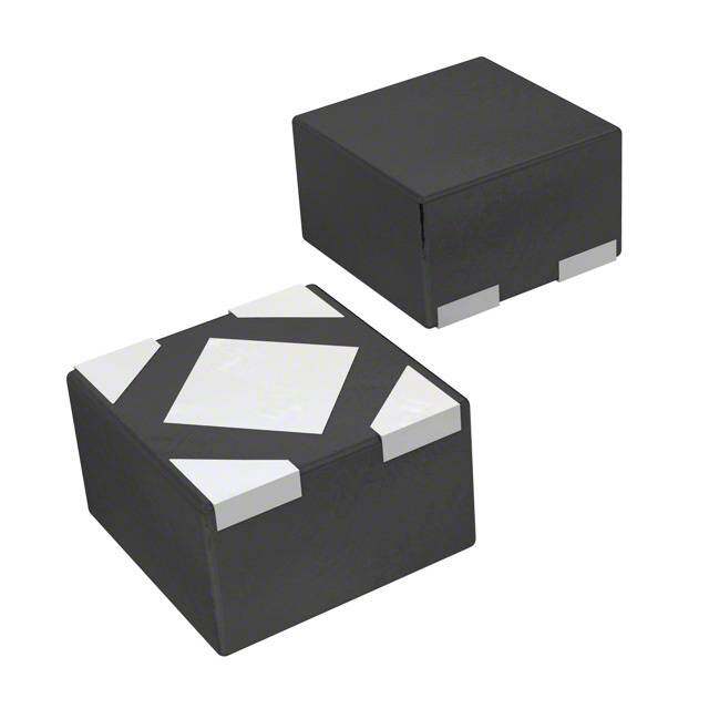
| 描述 | IC REG LDO ADJ 2A 10DFN低压差稳压器 SNG 2A ADJVVOUTLDO 3X310LDDFNW/ANNEAL1 |
| 产品分类 | |
| 品牌 | Intersil |
| 产品手册 | |
| 产品图片 |
|
| rohs | 符合RoHS无铅 / 符合限制有害物质指令(RoHS)规范要求 |
| 产品系列 | 电源管理 IC,低压差稳压器,Intersil ISL80102IRAJZ-TK- |
| 数据手册 | |
| 产品型号 | ISL80102IRAJZ-TK |
| 产品培训模块 | http://www.digikey.cn/PTM/IndividualPTM.page?site=cn&lang=zhs&ptm=25534 |
| 产品种类 | 低压差稳压器 |
| 供应商器件封装 | 10-DFN(3x3) |
| 其它名称 | ISL80102IRAJZ-TK-ND |
| 包装 | 带卷 (TR) |
| 商标 | Intersil |
| 回动电压—最大值 | 0.125 V at 2 A |
| 安装类型 | 表面贴装 |
| 安装风格 | SMD/SMT |
| 封装 | Reel |
| 封装/外壳 | 10-VFDFN 裸露焊盘 |
| 封装/箱体 | DFN EP |
| 工作温度 | -40°C ~ 125°C |
| 工厂包装数量 | 1000 |
| 最大工作温度 | + 125 C |
| 最大输入电压 | 6 V |
| 最小工作温度 | - 40 C |
| 最小输入电压 | 2.2 V |
| 标准包装 | 1,000 |
| 电压-跌落(典型值) | 0.081V @ 2A |
| 电压-输入 | 2.2 V ~ 6 V |
| 电压-输出 | 0.8 V ~ 5 V |
| 电压调节准确度 | +/- 0.5 % |
| 电流-输出 | 2A |
| 电流-限制(最小值) | - |
| 稳压器拓扑 | 正,可调式 |
| 稳压器数 | 1 |
| 系列 | ISL80102 |
| 线路调整率 | 0.1 % |
| 负载调节 | - 0.6 % |
| 输出电压 | 0.8 V to 5 V |
| 输出电流 | 3 A |
| 输出端数量 | 1 Output |
| 输出类型 | Adjustable |


- 商务部:美国ITC正式对集成电路等产品启动337调查
- 曝三星4nm工艺存在良率问题 高通将骁龙8 Gen1或转产台积电
- 太阳诱电将投资9.5亿元在常州建新厂生产MLCC 预计2023年完工
- 英特尔发布欧洲新工厂建设计划 深化IDM 2.0 战略
- 台积电先进制程称霸业界 有大客户加持明年业绩稳了
- 达到5530亿美元!SIA预计今年全球半导体销售额将创下新高
- 英特尔拟将自动驾驶子公司Mobileye上市 估值或超500亿美元
- 三星加码芯片和SET,合并消费电子和移动部门,撤换高东真等 CEO
- 三星电子宣布重大人事变动 还合并消费电子和移动部门
- 海关总署:前11个月进口集成电路产品价值2.52万亿元 增长14.8%


PDF Datasheet 数据手册内容提取
DATASHEET ISL80102, ISL80103 FN6660 High Performance 2A and 3A Linear Regulators Rev.9.02 Jun 11, 2020 The ISL80102 and ISL80103 are low voltage, high-current, Features single output LDOs specified for 2A and 3A output current, respectively. These LDOs operate from the input voltages of • Stable with ceramic capacitors (Note11) 2.2V to 6V and are capable of providing the output voltages of • 2A and 3A output current ratings 0.8V to 5.5V. • 2.2V to 6V input voltage range An external capacitor on the soft-start pin provides adjustment • ±1.8% VOUT accuracy assured over line, load, and TJ=-40°C for applications that demand inrush current less than the to +125°C current limit. The ENABLE feature allows the part to be placed • Very low 120mV dropout voltage at 3A (ISL80103) into a low quiescent current shutdown mode. A submicron BiCMOS process is used for this product family to deliver • Very fast transient response best-in-class analog performance and overall value. • Excellent 62dB PSRR These CMOS (LDOs) consume significantly lower quiescent • 49µVRMS output noise current as a function of load over bipolar LDOs, so they are • Power-good output more efficient and allow packages with smaller footprints. The quiescent current has been modestly compromised to enable • Adjustable inrush current limiting a leading class fast load transient response, and hence a lower • Short-circuit and over-temperature protection total AC regulation band for an LDO in this category. • Available in a 10 Ld DFN Related Literature Applications For a full list of related documents, visit our website • Servers •ISL80102, ISL80103 product pages • Telecommunications and networking • Medical equipment • Instrumentation systems • Routers and switchers ISL80102, ISL80103 1.8V 2.5V ±10% 9 1 VIN VIN VOUT VOUT CIN 10 VIN VOUT 2 COUT 10µF 10µF RPG R1 100kΩ 10kΩ 4 PG PGOOD 7 EN ENABLE OPEN DRAIN COMPATIBLE 6 **CPB R3 SS 47pF 2.61kΩ 3 *CSS ADJ GND 5 R4 1.0kΩ *CSS is optional (see Note12 on page5). **CPB is optional (see “Functional Description” on page12 for more information). FIGURE 1. TYPICAL APPLICATION DIAGRAM FOR ADJUSTABLE OUTPUT VOLTAGE VERSION FN6660 Rev.9.02 Page 1 of 16 Jun 11, 2020
ISL80102, ISL80103 Pin Descriptions TABLE 1. COMPONENTS VALUE SELECTION VOUT RTOP RBOTTOM CPB COUT PIN PIN (V) (kΩ) (Ω) (pF) (µF) NUMBER NAME DESCRIPTION 5.0 2.61 287 47 10 1, 2 VOUT Output voltage pin 3.3 2.61 464 47 10 3 ADJ ADJ pin for externally set VOUT. 2.5 2.61 649 47 10 4 PG VOUT in regulation signal. Logic low defines when 1.8 (Note1) 2.61 1.0k 47 10 VusOeUdT. is not in regulation. Must be grounded if not 1.8 (Note1) 2.61 1.0k 82 22 5 GND GND pin 1.5 2.61 1.3k 82 22 6 SS External cap adjusts inrush current. Leave this pin open if not used. 1.2 2.61 1.87k 150 47 1.0 2.61 2.61k 150 47 7 ENABLE VIN independent chip enable. TTL and CMOS compatible. 0.8 2.61 4.32k 150 47 8 DNC Do not connect this pin to ground or supply. Leave NOTE: floating. 1. Either option can be used depending on cost/performance requirements 9, 10 VIN Input supply pin EPAD EPAD must be connected to a copper plane with as Pin Configuration many vias as possible for proper electrical and optimal thermal performance. 10 LD 3x3 DFN TOP VIEW Block Diagram VOUT 1 10 VIN VOUT 2 9 VIN ADJ 3 EPAD 8 DNC PG 4 7 ENABLE GND 5 6 SS VIN R5 IL/10000 10µA 10µA M5 M4 M3 M1 POWER PMOS IL VOUT R8 + M6 - R7 R9 EN - R1 500mV EN + EN R4 + ADJ EENN - ENABLE M7 PG - 500mV ++ M2 SS V TO I -- + M8 EN 485mV +- *R3 GND *R3 is open for ADJ versions. FIGURE 2. BLOCK DIAGRAM FN6660 Rev.9.02 Page 2 of 16 Jun 11, 2020
ISL80102, ISL80103 Ordering Information PART NUMBER PART VOUT TEMP. RANGE TAPE AND REEL PACKAGE PKG (Notes2, 4, 4) MARKING VOLTAGE (°C) (Units) (Note 1) (RoHS COMPLIANT) DWG. # ISL80102IRAJZ DZJA ADJ -40 to +125 - 10 Ld 3x3 DFN L10.3x3 ISL80102IRAJZ-T DZJA ADJ -40 to +125 6k 10 Ld 3x3 DFN L10.3x3 ISL80102IRAJZ-TK DZJA ADJ -40 to +125 1k 10 Ld 3x3 DFN L10.3x3 ISL80102IRAJZ-T7A DZJA ADJ -40 to +125 250 10 Ld 3x3 DFN L10.3x3 ISL80103IRAJZ DZAA ADJ -40 to +125 - 10 Ld 3x3 DFN L10.3x3 ISL80103IRAJZ-T DZAA ADJ -40 to +125 6k 10 Ld 3x3 DFN L10.3x3 ISL80103IRAJZ-TK DZAA ADJ -40 to +125 4k 10 Ld 3x3 DFN L10.3x3 ISL80103IRAJZ-T7A DZAA ADJ -40 to +125 250 10 Ld 3x3 DFN L10.3x3 ISL80102EVAL2Z Evaluation Board ISL80103EVAL2Z Evaluation Board NOTES: 2. See TB347 for details about reel specifications. 3. These Pb-free plastic packaged products employ special Pb-free material sets, molding compounds/die attach materials, and 100% matte tin plate plus anneal (e3 termination finish, which is RoHS compliant and compatible with both SnPb and Pb-free soldering operations). Pb-free products are MSL classified at Pb-free peak reflow temperatures that meet or exceed the Pb-free requirements of IPC/JEDEC J STD-020. 4. For Moisture Sensitivity Level (MSL), see the ISL80102 and ISL80103 product information pages. For more information about MSL, see TB363. FN6660 Rev.9.02 Page 3 of 16 Jun 11, 2020
ISL80102, ISL80103 Absolute Maximum Ratings Thermal Information (Note8) VIN Relative to GND . . . . . . . . . . . . . . . . . . . . . . . . . . . . . . . . . -0.3V to +6.5V Thermal Resistance (Typical) JA (°C/W) JC (°C/W) VOUT Relative to GND . . . . . . . . . . . . . . . . . . . . . . . . . . . . . . . -0.3V to +6.5V 10 Ld 3x3 DFN Package (Notes5, 6) . . . . 45 4 PG, ENABLE, ADJ, SS, Relative to GND . . . . . . . . . . . . . . . . . -0.3V to +6.5V θJB at Pin 3 (Note7). . . . . . . . . . . . . . . . . . . . . . . . . . . . . . . . . . . . 14.7°C/W ESD Rating θJB at Pin 5 (Note7). . . . . . . . . . . . . . . . . . . . . . . . . . . . . . . . . . . . . .8.9°C/W Human Body Model (Tested per JESD22 A114F). . . . . . . . . . . . . . .2.2kV Maximum Junction Temperature (Plastic Package) . . . . . . . . . . . .+150°C Charge Device Model (Tested per JESD22-C101C) . . . . . . . . . . . . . . 1kV Storage Temperature Range. . . . . . . . . . . . . . . . . . . . . . . .-65°C to +150°C Latch-up (Tested per JESD78C, Class 2, Level A). . . . . ±100mA at +85°C Pb-Free Reflow Profile. . . . . . . . . . . . . . . . . . . . . . . . . . . . . . . . . . see TB493 Recommended Operating Conditions Junction Temperature Range (TJ) . . . . . . . . . . . . . . . . . . .-40°C to +125°C VIN Relative to GND . . . . . . . . . . . . . . . . . . . . . . . . . . . . . . . . . . . . .2.2V to 6V VOUT Range. . . . . . . . . . . . . . . . . . . . . . . . . . . . . . . . . . . . . . . 800mV to 5.5V PG, ENABLE, ADJ, SS Relative to GND. . . . . . . . . . . . . . . . . . . . . . . 0V to 6V PG Sink Current . . . . . . . . . . . . . . . . . . . . . . . . . . . . . . . . . . . . . . . . . . . 10mA CAUTION: Do not operate at or near the maximum ratings listed for extended periods of time. Exposure to such conditions can adversely impact product reliability and result in failures not covered by warranty. NOTES: 5. θJA is measured in free air with the component mounted on a high-effective thermal conductivity test board with “direct attach” features. See TB379. 6. For θJC, the “case temp” location is the center of the exposed metal pad on the package underside. 7. For θJB, the board temperature is taken on the board near the edge of the package, on a copper trace at either lead #3 or lead #5, as applicable. See TB379 8. ABS max voltage rating is defined as the voltage applied for a lifetime average duty cycle above 6V of 1%. Electrical Specifications Unless otherwise noted, all parameters are established over the following specified conditions: 2.2V < VIN < 6V, VOUT = 0.5V, TJ = +25°C, ILOAD = 0A. Applications must follow thermal guidelines of the package to determine worst case junction temperature. Refer to “Functional Description” on page12 and TB379. Boldface limits apply across the operating temperature range, -40°C to +125°C. Pulse load techniques used by ATE to ensure TJ = TA defines established limits. MIN MAX PARAMETER SYMBOL TEST CONDITIONS (Note9) TYP (Note9) UNIT DC CHARACTERISTICS DC Output Voltage Accuracy VOUT 2.2V < VIN < 6V; ILOAD = 0A 0.5 % 2.2V < VIN < 6V; 0A < ILOAD < 3A -1.8 1.8 % 2.9V < VIN < 6V; ILOAD = 0A 0.5 % 2.9V < VIN < 6V; 0A < ILOAD < full load -1.8 -1.8 % Feedback Pin VADJ 0A < ILOAD < full load 491 500 509 mV DC Input Line Regulation (VOUT Low Line-VOUT 2.2V < VIN < 3.6V, VOUT = 1.8V -0.4 0.1 0.4 % High Line)/ VOUT Low Line 2.9V < VIN < 6V, VOUT = 2.5V -0.8 0.1 0.8 % DC Output Load Regulation (VOUT No Load - VOUT ISL80103, 0A < ILOAD < 3A, -0.8 -0.2 0.8 % High Load)/ 2.9V < VIN < 6V; VOUT = 2.5V VOUT No Load ISL80102, 0A < ILOAD < 2A -0.6 -0.2 0.6 % 2.9V < VIN < 6V; VOUT = 2.5V Feedback Input Current VADJ = 0.5V 0.01 1 µA Ground Pin Current IQ ILOAD = 0A, VOUT + 0.4V < VIN < 6V 7.5 9 mA VOUT = 2.5V ILOAD = 3A, VOUT + 0.4V < VIN < 6V 8.5 12 mA VOUT = 2.5V Ground Pin Current in Shutdown ISHDN EN = 0V, VIN = 5V 0.4 µA EN = 0V, VIN = 6V 3.3 16.0 µA FN6660 Rev.9.02 Page 4 of 16 Jun 11, 2020
ISL80102, ISL80103 Electrical Specifications Unless otherwise noted, all parameters are established over the following specified conditions: 2.2V < VIN < 6V, VOUT = 0.5V, TJ = +25°C, ILOAD = 0A. Applications must follow thermal guidelines of the package to determine worst case junction temperature. Refer to “Functional Description” on page12 and TB379. Boldface limits apply across the operating temperature range, -40°C to +125°C. Pulse load techniques used by ATE to ensure TJ = TA defines established limits. (Continued) MIN MAX PARAMETER SYMBOL TEST CONDITIONS (Note9) TYP (Note9) UNIT Dropout Voltage (Note10) VDO ISL80103, ILOAD = 3A, VOUT = 2.5V 120 185 mV ISL80102, ILOAD = 2A, VOUT = 2.5V 81 125 mV ISL80103, ILOAD = 3A, VOUT = 5.5V 120 244 mV ISL80102, ILOAD = 2A, VOUT = 5.5V 60 121 mV Output Short-Circuit Current ISC ISL80103, VOUT = 0V 5.0 A (3AVersion) Output Short-Circuit Current ISL80102, VOUT = 0V 2.8 A (2AVersion) Thermal Shutdown Temperature TSD 160 °C Thermal Shutdown Hysteresis TSDn 15 °C AC CHARACTERISTICS Input Supply Ripple Rejection PSRR f = 1kHz, ILOAD = 1A; VIN = 2.2V 55 dB f = 120Hz, ILOAD = 1A; VIN = 2.2V 62 dB Output Noise Voltage VIN = 2.2V, VOUT = 1.8V, ILOAD = 3A, 49 µVRMS BW = 100Hz < f<100kHz ENABLE PIN CHARACTERISTICS Turn-On Threshold VEN(HIGH) 2.2V < VIN < 6V 0.616 0.800 0.950 V Turn-Off Threshold VEN(LOW) 2.2V < VIN < 6V 0.463 0.600 V Hysteresis VEN(HYS) 2.2V < VIN < 6V 135 mV Enable Pin Turn-On Delay tEN COUT = 10µF, ILOAD = 1A 150 µs Enable Pin Leakage Current VIN = 6V, EN = 3V 1 µA SOFT-START CHARACTERISTICS Reset Pull-Down Resistance RPD 323 Ω Soft-Start Charge Current ICHG -7.0 -4.5 -2.0 µA PG PIN CHARACTERISTICS VOUT PG Flag Threshold 75 84 92 %VOUT VOUT PG Flag Hysteresis 4 % PG Flag Low Voltage ISINK = 500µA 47 100 mV PG Flag Leakage Current VIN = 6V, PG = 6V 0.05 1 µA NOTES: 9. Compliance to datasheet limits is assured by one or more methods: production test, characterization, and/or design. 10. Dropout is defined by the difference in supply VIN and VOUT when the supply produces a 2% drop in VOUT from its nominal value. 11. Minimum cap of 10µF X5R/X7R on VIN and VOUT required for stability. 12. If the current limit for inrush current is acceptable in the application, do not use this feature (leave the SS pin open). Use only when large bulk capacitance is required on VOUT for the application. FN6660 Rev.9.02 Page 5 of 16 Jun 11, 2020
ISL80102, ISL80103 Typical Operating Performance Unless otherwise noted, VIN = 2.2V, VOUT = 1.8V, CIN = COUT = 10µF, TJ = +25°C, IL = 0A. 1.8 2.0 1.8 1.2 1.6 V) 0.6 GE ( 1.4 +125°C %) A 1.2 V (OUT 0 T VOLT 01..80 +25°C -40°C U -0.6 P T 0.6 U O 0.4 -1.2 0.2 -1.8 0 -50 -25 0 25 50 75 100 125 150 0 1 2 3 4 5 6 JUNCTION TEMPERATURE (°C) SUPPLY VOLTAGE (V) FIGURE 3. VOUT vs TEMPERATURE FIGURE 4. OUTPUT VOLTAGE vs SUPPLY VOLTAGE 1.8 9 8 1.2 A) 7 m 0.6 T ( 6 %) +25°C EN V (OUT 0.0 D CURR 45 -0.6 N 3 U O -40°C R 2 -1.2 G +125°C 1 -1.8 0 0 0.5 1.0 1.5 2.0 2.5 3.0 2 3 4 5 6 OUTPUT CURRENT (A) INPUT VOLTAGE (V) FIGURE 5. VOUT vs OUTPUT CURRENT FIGURE 6. GROUND CURRENT vs SUPPLY VOLTAGE 9.1 12.0 8.9 11.5 mA) 8.7 11.0 -40°C T ( -40°C A) 10.5 N 8.5 m CURRE 8.3 +25°C RENT ( 109..05 D 8.1 R N U 9.0 +125°C U C O 7.9 +125°C R 8.5 G 7.7 8.0 +25°C 7.5 7.5 0 0.5 1.0 1.5 2.0 2.5 3.0 0.8 1.4 2.0 2.6 3.2 3.8 4.4 5.0 OUTPUT CURRENT (A) OUTPUT VOLTAGE (V) FIGURE 7. GROUND CURRENT vs OUTPUT CURRENT FIGURE 8. GROUND CURRENT vs OUTPUT VOLTAGE (VIN = VOUT + VDO) FN6660 Rev.9.02 Page 6 of 16 Jun 11, 2020
ISL80102, ISL80103 Typical Operating Performance Unless otherwise noted, VIN = 2.2V, VOUT = 1.8V, CIN = COUT = 10µF, TJ = +25°C, IL = 0A. (Continued) 5.0 12 4.5 11 A) 4.0 A) 10 NT (µ 3.5 NT (µ 89 RE 3.0 RE 7 UR 2.5 UR 6 C C D 2.0 D 5 UN 1.5 UN 4 GRO 1.0 GRO 23 0.5 VIN = 5V 1 VIN = 6V 0.0 0 -40 -25 -10 5 20 35 50 65 80 95 110 125 -40 -25 -10 5 20 35 50 65 80 95 110 125 TEMPERATURE (°C) TEMPERATURE (°C) FIGURE 9. GROUND CURRENT IN SHUTDOWN vs TEMPERATURE FIGURE 10. GROUND CURRENT IN SHUTDOWN vs TEMPERATURE 150 150 140 140 130 130 V) 120 V) 120 m m GE ( 110100 2A GE ( 110100 A 90 3A A 90 T T L 80 L 80 O O V 70 V 70 UT 60 UT 60 O 50 O 50 OP 40 OP 40 R 30 R 30 D D 20 1A 20 10 10 0 0 -40 -25 -10 5 20 35 50 65 80 95 110 125 0 0.5 1.0 1.5 2.0 2.5 3.0 TEMPERATURE (°C) OUTPUT CURRENT (A) FIGURE 11. DROPOUT VOLTAGE vs TEMPERATURE FIGURE 12. DROPOUT VOLTAGE vs OUTPUT CURRENT 0.90 0.85 0.80 0.75 V) 0.70 E ( 0.65 G A 0.60 T L 0.55 O V 0.50 0.45 0.40 0.35 0.30 -40 -25 -10 5 20 35 50 65 80 95 110 125 JUNCTION TEMPERATURE (°C) FIGURE 13. ENABLE THRESHOLD VOLTAGE vs TEMPERATURE FN6660 Rev.9.02 Page 7 of 16 Jun 11, 2020
ISL80102, ISL80103 Typical Operating Performance Unless otherwise noted, VIN = 2.2V, VOUT = 1.8V, CIN = COUT = 10µF, TJ = +25°C, IL = 0A. (Continued) EN (1V/DIV) EN (1V/DIV) SS (500mV/DIV) SS (200mV/DIV) VOUT (500mV/DIV) PG (1V/DIV) VOUT (500mV/DIV) PG (1V/DIV) TIME (50µs/DIV) TIME (6.4ms/DIV) FIGURE 14. ENABLE START-UP SS CAP 1nF FIGURE 15. ENABLE SHUTDOWN SS CAP 1nF EN (1V/DIV) EN (1V/DIV) SS (1V/DIV) SS (200mV/DIV) VOUT (1V/DIV) PG (1V/DIV) VOUT (500mV/DIV) PG (1V/DIV) TIME (2ms/DIV) TIME (50µs/DIV) FIGURE 16. ENABLE START-UP SS CAP 100nF FIGURE 17. ENABLE START-UP (NO SS CAP) 300 EN (1V/DIV) 250 s) µ E ( 200 SS (1V/DIV) M TI P 150 U T- VOUT (1V/DIV) TAR 100 S 50 PG (1V/DIV) 0 2.0 2.5 3.0 3.5 4.0 4.5 5.0 5.5 6.0 TIME (5ms/DIV) INPUT VOLTAGE (V) FIGURE 18. ENABLE SHUTDOWN (NO SS CAP) FIGURE 19. START-UP TIME vs SUPPLY VOLTAGE FN6660 Rev.9.02 Page 8 of 16 Jun 11, 2020
ISL80102, ISL80103 Typical Operating Performance Unless otherwise noted, VIN = 2.2V, VOUT = 1.8V, CIN = COUT = 10µF, TJ = +25°C, IL = 0A. (Continued) 300 7.0 6.5 250 6.0 ME (µs) 200 RENT (A) 4455....0505 ISL80103 TI R P 150 U 3.5 T-U T C 3.0 ISL80102 AR 100 PU 2.5 T T 2.0 S U O 1.5 50 1.0 0.5 0 0 -40 -25 -10 5 20 35 50 65 80 95 110 125 -40 -25 -10 5 20 35 50 65 80 95 110 125 JUNCTION TEMPERATURE (°C) TEMPERATURE (°C) FIGURE 20. START-UP TIME vs TEMPERATURE FIGURE 21. CURRENT LIMIT vs TEMPERATURE 7.0 IOUT (1A/DIV) 6.5 6.0 A) 5.5 T ( 5.0 ISL80103 N 4.5 E R 4.0 R U 3.5 T C 3.0 ISL80102 U 2.5 P T 2.0 U O 1.5 VOUT (1V/DIV) 1.0 0.5 0 2.0 2.5 3.0 3.5 4.0 4.5 5.0 5.5 6.0 INPUT VOLTAGE(V) TIME (10ms/DIV) FIGURE 22. CURRENT LIMIT vs SUPPLY VOLTAGE FIGURE 23. CURRENT LIMIT RESPONSE (ISL80102) EN (1V/DIV) IOUT (2A/DIV) IINRUSH (2A/DIV) VOUT (1V/DIV) VOUT (1V/DIV) PG (1V/DIV) TIME (5ms/DIV) TIME (200µs/DIV) FIGURE 24. CURRENT LIMIT RESPONSE (ISL80103) FIGURE 25. INRUSH CURRENT WITH NO SOFT-START CAPACITOR, COUT = 1000µF FN6660 Rev.9.02 Page 9 of 16 Jun 11, 2020
ISL80102, ISL80103 Typical Operating Performance Unless otherwise noted, VIN = 2.2V, VOUT = 1.8V, CIN = COUT = 10µF, TJ = +25°C, IL = 0A. (Continued) EN (1V/DIV) VOUT (50mV/DIV) IINRUSH (1A/DIV) VOUT (1V/DIV) IOUT (2A/DIV) PG (1V/DIV) di/dt = 30A/µs TIME (1ms/DIV) TIME (200µs/DIV) FIGURE 26. INRUSH WITH 22nF SOFT-START CAPACITOR, FIGURE 27. LOAD TRANSIENT 0A TO 3A, COUT=10µF CERAMIC COUT=1000µF VOUT (50mV/DIV) VOUT (50mV/DIV) IOUT (2A/DIV) IOUT (2A/DIV) di/dt = 30A/µs di/dt = 30A/µs TIME (200µs/DIV) TIME (200µs/DIV) FIGURE 28. LOAD TRANSIENT 0A TO 3A, COUT=10µF FIGURE 29. LOAD TRANSIENT 1A TO 3A, COUT=10µF CERAMIC CERAMIC + 100µF OSCON VOUT (20mV/DIV) VOUT (50mV/DIV) IOUT (2A/DIV) IOUT (2A/DIV) di/dt = 30A/µs di/dt = 3A/µs TIME (200µs/DIV) TIME (50µs/DIV) FIGURE 30. LOAD TRANSIENT 1A TO 3A, COUT=10µF FIGURE 31. LOAD TRANSIENT 0A TO 3A, COUT=10µF CERAMIC, CERAMIC + 100µF OSCON NOCPB FN6660 Rev.9.02 Page 10 of 16 Jun 11, 2020
ISL80102, ISL80103 Typical Operating Performance Unless otherwise noted, VIN = 2.2V, VOUT = 1.8V, CIN = COUT = 10µF, TJ = +25°C, IL = 0A. (Continued) 3.2V 2.2V VOUT (20mV/DIV) VIN (1V/DIV) di/dt = 3A/sec IOUT (2A/DIV) di/dt = 3A/µs VOUT (10mV/DIV) TIME (50µs/DIV) TIME (200µs/DIV) FIGURE 32. LOAD TRANSIENT 0A TO 3A, COUT=10µF CERAMIC, FIGURE 33. LINE TRANSIENT CPB= 1500pF 90 90 80 80 NO LOAD 70 100mA 70 60 NO LOAD 60 B) B) d 50 d 50 R ( R ( 100mA R 40 R 40 S S P P 30 1000mA 30 1000mA 20 300mA 20 300mA 10 10 0 0 10 100 1k 10k 100k 1M 10 100 1k 10k 100k 1M FREQUENCY (Hz) FREQUENCY (Hz) FIGURE 34. PSRR vs FREQUENCY FOR VOUT = 1.0V, VIN = 2.5V; FIGURE 35. PSRR vs FREQUENCY FOR VOUT = 1.2V; VIN = 2.5V; COUT= 47µF, CPB = 150pF COUT= 47µF, CPB = 150pF 90 90 300mA 100mA 1000mA 100mA 80 80 70 70 60 60 NO LOAD B) NO LOAD B) d 50 2000mA 1000mA d 50 2000mA R ( R ( 3000mA R 40 R 40 S S P P 30 30 20 20 300mA 10 10 0 0 10 100 1k 10k 100k 1M 10 100 1k 10k 100k 1M FREQUENCY (Hz) FREQUENCY (Hz) FIGURE 36. PSRR vs FREQUENCY FOR VOUT = 1.5V, VIN = 2.5V; FIGURE 37. PSRR vs FREQUENCY FOR VOUT = 1.8V, VIN = 2.5V; COUT= 22µF, CPB = 82pF COUT= 22µF, CPB = 82pF FN6660 Rev.9.02 Page 11 of 16 Jun 11, 2020
ISL80102, ISL80103 Typical Operating Performance Unless otherwise noted, VIN = 2.2V, VOUT = 1.8V, CIN = COUT = 10µF, TJ = +25°C, IL = 0A. (Continued) 90 10 100mA 80 300mA 70 60 z 1 RR (dB) 4500 2000mA 1000mA NO LOAD E µV/√H S S P OI 30 3000mA N 0.1 20 10 IL = 3A 0 0.01 10 100 1k 10k 100k 1M 10 100 1k 10k 100k 1M FREQUENCY (Hz) FREQUENCY (Hz) FIGURE 38. PSRR vs FREQUENCY FOR VOUT = 2.5V, VIN = 3.3V; FIGURE 39. SPECTRAL NOISE DENSITY vs FREQUENCY COUT= 10µF, CPB = 47pF Functional Description Soft-Start Operation (Optional) If the current limit for inrush current is acceptable in the Input Voltage Requirements application, do not use the soft-start (SS) feature (leave the SS This family of LDOs is optimized for a true 2.5V to 1.8V pin open). The soft-start circuit controls the rate at which the conversion in which the input supply can have a tolerance of as output voltage comes up to regulation at power-up or LDO much as ±10% for conditions noted in the “Electrical enable. The external soft-start capacitor always gets discharged Specifications” table on page4. The minimum guaranteed input to ground pin potential at the beginning of start-up or enabling. voltage is 2.2V; however, due to the nature of an LDO, VIN must After the capacitor discharges, it will immediately begin charging be some margin higher than the output voltage plus dropout at by a constant current source. The discharge rate is the RC time the maximum rated current of the application if active filtering constant of RPD and CSS. Refer to Figures14 through 18 in the (PSRR) is expected from VIN to VOUT. The dropout of this family of “Typical Operating Performance Curves” beginning on page8. LDOs has been generously specified to allow applications to RPD is the ON-resistance of the pull-down MOSFET, M8. RPD is design for a level of efficiency that can accommodate the typically 323Ω. smaller outline package. The soft-start feature effectively reduces the inrush current at Enable Operation power-up or LDO enable until VOUT reaches regulation. The in-rush current can be an issue for applications that require large, The Enable turn-on threshold is typically 800mV with a hysteresis of external bulk capacitances on VOUT where high levels of charging 135mV. This pin must not be left floating. This pin must be tied to current can be seen for a significant period of time. The inrush VIN if it is not used. A 1kΩ to 10kΩ pull-up resistor is required for currents can cause VIN to drop below minimum which could applications that use open collector or open drain outputs to control cause VOUT to shutdown. Figure26 on page10 shows the the Enable pin. The Enable pin can be connected directly to VIN for relationship between inrush current and CSS with a COUT of applications that are always on. 1000µF. Power-Good Operation 5.0 Applications not using the power-good (PGOOD) feature must 4.5 connect this pin to ground. The PGOOD flag is an open-drain T (A) 4.0 NMOS that can sink up to 10mA during a fault condition. The MI 3.5 PGOOD pin requires an external pull-up resistor, which is typically LI T 3.0 cuopn tnoe ac tveodlt taog teh seo VuOrcUeT gpriena. tTehre t hPaGnO VOIDN .p PinG OshOoDu lfda unlotst bcaen p buelle d RREN 2.5 U 2.0 caused by the output voltage going below 84% of the nominal C output voltage, or the current limit fault, or low input voltage. SH 1.5 U PGOOD does not function during thermal shutdown. R 1.0 N I 0.5 0 0 20 40 60 80 100 CSS (nF) FIGURE 40. INRUSH CURRENT vs SOFT-START CAPACITANCE FN6660 Rev.9.02 Page 12 of 16 Jun 11, 2020
ISL80102, ISL80103 Output Voltage Selection Current Limit Protection An external resistor divider scales the output voltage relative to The ISL80102 and ISL80103 family of LDOs incorporates the internal reference voltage. This voltage is then fed back to protection against overcurrent due to a short overload condition the error amplifier. The output voltage can be programmed to applied to the output and the inrush current that occurs at any level between 0.8V and 5.5V. An external resistor divider, R3 start-up. The LDO performs as a constant current source when and R4, sets the output voltage as shown in Equation1. The the output current exceeds the current limit threshold noted in recommended value for R4 is 200Ω to 5kΩR3is then chosen the “Electrical Specifications” table on page4. If the short or according to Equation2: overload condition is removed from VOUT, then the output returns to normal voltage mode regulation. In the event of an overload V = 0.5VR-----3--+1 (EQ. 1) condition, the LDO may begin to cycle on and off due to the die OUT R4 temperature exceeding the thermal fault condition. V Power Dissipation and Thermals R = R -----O----U----T---–1 (EQ. 2) 3 4 0.5V The junction temperature must not exceed the range specified in External Capacitor Requirements the “Recommended Operating Conditions” on page4. The power dissipation can be calculated by using Equation3: External capacitors are required for proper operation. To ensure P = V –V I +V I (EQ. 3) optimal performance, pay careful attention to the layout D IN OUT OUT IN GND guidelines and selection of capacitor type and value. The maximum allowable junction temperature, TJ(MAX) and the OUTPUT CAPACITOR maximum expected ambient temperature, TA(MAX) determine the maximum allowable power dissipation as shown in Equation4: The ISL80102 and ISL80103 apply state-of-the-art internal P = T –T (EQ. 4) compensation to keep selection of the output capacitor simple DMAX JMAX A JA for the customer. Stable operation over full temperature, VIN where JA is the junction-to-ambient thermal resistance. range, VOUT range, and load extremes are guaranteed for all ceramic capacitors and values assuming a 10µF X5R/X7R is For safe operation, ensure that the power dissipation calculated used for local bypass on VOUT. This minimum capacitor (see in Equation3, PD, is less than the maximum allowable power Table1 on page2 for component value selections) must be dissipation PD(MAX). connected to the VOUT and ground pins of the LDO with PCB The DFN package uses the copper area on the PCB as a heatsink. traces no longer than 0.5cm. The EPAD of this package must be soldered to the copper plane Lower cost Y5V and Z5U type ceramic capacitors are acceptable (GND plane) for heat sinking. Figure41 shows a curve for the JA if the size of the capacitor is large enough to compensate for the of the DFN package for different copper area sizes. significantly lower tolerance over X5R/X7R types. Additional capacitors of any value in Ceramic, POSCAP, or Alum/Tantalum 46 Electrolytic types can be placed in parallel to improve PSRR at 44 higher frequencies and/or load transient AC output voltage tolerances. 42 W) INPUT CAPACITOR C/ 40 The minimum input capacitor required for proper operation is a (°A J 38 10µF with a ceramic dielectric. This minimum capacitor must be connected to VIN and ground pins of the LDO with PCB traces no 36 longer than 0.5cm. 34 Phase Boost Capacitor (Optional) 2 4 6 8 10 12 14 16 18 20 22 24 The ISL80102 and ISL80103 are designed to be stable with EPAD-MOUNT COPPER LAND AREA ON PCB, mm2 10µF or larger ceramic capacitors. FIGURE 41. 3mmx3mm-10 PIN DFN ON 4-LAYER PCB WITH THERMAL VIAS JA vs EPAD-MOUNT COPPER LAND Applications can see improved performance with the addition of AREA ON PCB a small ceramic capacitor CPB as shown in Figure1 on page1. The conditions in which CPB may be beneficial are: Thermal Fault Protection • VOUT > 1.5V If the die temperature exceeds typically +160°C, the output of • COUT = 10µF the LDO shuts down until the die temperature can cool down to typically +145°C. The level of power combined with the thermal • Tight AC voltage regulation band impedance of the package (+48°C/W for DFN) determine if the CPB introduces phase lead with the product of R3 and CPB that junction temperature exceeds the thermal shutdown results in increasing the bandwidth of the LDO. Typical R3 x CPB temperature. should be less than 0.4μs (400ns). FN6660 Rev.9.02 Page 13 of 16 Jun 11, 2020
ISL80102, ISL80103 Revision History The revision history provided is for informational purposes only and is believed to be accurate, but not warranted. Please go to web to make sure you have the latest revision. DATE REVISION CHANGE Jun 11, 2020 9.02 Updated Ordering Information table by removing retired parts, adding tape and reel info, and updated notes. Removed information throughout the document related to the retired parts. Added Theta JB information. Dec 3, 2019 9.01 Updated Links throughout. Updated Figures 15 and 17. Updated disclaimer. Mar 19, 2018 9.00 Added Related Literature section to page 1. Changed values in Output Voltage Selection section on page 13 from “500Ω to 1kΩ” to “200Ω to 5kΩ”. Removed About Intersil section and added Renesas disclaimer. Sep 2, 2016 8.00 Removed Note 8 “Electromigration specification defined as lifetime average junction temperature of +110°C where max rated DC current = lifetime average current” from Recommended Operating Conditions. Apr 8, 2016 7.00 Updated Ordering Information table (on page3), Note 1 to include quantities for tape and reel options. Changed VOUT range upper limit from “5V to 5.5V” on page 1, in the “Recommended Operating Conditions (Note7)” on page 4 and in the “Output Voltage Selection” on page 12 Electrical Spec table test conditions changed from: VIN=VOUT + 0.4V, VOUT = 1.8V, CIN = COUT = 10µF, TJ = +25°C, ILOAD = 0A, to: 2.2V < VIN < 6V, VOUT = 0,5V, TJ = +25°C, ILOAD = 0A Changed Test conditions in “Output Noise Voltage” on page 5 from: ILOAD = 10mA, BW = 300Hz <f< 300kHz; to: VIN = 2.2V, VOUT = 1.8V, ILOAD = 3A, BW = 100Hz<f<100kHz and changed TYP from: 100; to: 49 Added two rows to “Dropout Voltage (Note 9)” on page 5 to show parameters for 5.5V VOUT conditions. Updated verbiage for “About Intersil” on page 16. Updated POD L10.3x3 to most updated revision with changes as follows: Added missing dimension 0.415 in Typical Recommended land pattern. Shortened the e-pad rectangle on both the recommended land pattern and the package bottom view to line up with the centers of the corner pins. Changed Tiebar note 4, from: Tiebar shown (if present) is a non-functional feature. to: Tiebar shown (if present) is a non-functional feature and may be located on any of the 4 sides (or ends). May 23, 2013 6.00 Pin Descriptions on pagepage2, updated EPAD section From: EPAD at ground potential. Soldering it directly to GND plane is optional. To: EPAD must be connected to copper plane with as many vias as possible for proper electrical and optimal thermal performance. Removed obsolete part numbers: ISL80102IR33Z, ISL80102IR50Z, ISL80103IR33Z, ISL80103IR50Z from ordering information table on page3. Added evaluation boards to ordering information table on page3: ISL80103IR50Z and ISL80103EVAL2Z. Features on page1: Removed 5 Ld TO220 and 5 Ld TO263. Input Voltage Requirements on page12: Removed the sentence “those applications that cannot accommodate the profile of the TO220/TO263”. Jun 14, 2012 5.00 In “Thermal Information” on page4, corrected JA from 48 to 45. Feb 14, 2012 4.00 Increased “VEN(HIGH)” minimum limit from 0.4V to 0.616 and added the “VEN(LOW)” spec for clarity on page5. Dec 14, 2011 3.00 Increased “Turn-on Threshold” minimum limit on page5 from 0.3V to 0.4V. Updated “Package Outline Drawing” on page16 as follows: Removed package outline and included center to center distance between lands on recommended land pattern. Removed Note 4 "Dimension b applies to the metallized terminal and is measured between 0.18mm and 0.30mm from the terminal tip." since it is not applicable to this package. Renumbered notes accordingly. Mar 4, 2011 2.00 Converted to new template On page1 - first paragraph, changed "Fixed output voltage options are available in 1.5V, 1.8V, 2.5V, 3.3V and 5V" to "Fixed output voltage options are available in 1.8V, 2.5V, 3.3V and 5V" In “Ordering Information” table on page2, removed ISL80102IR15Z and ISL80103IR15Z. In Note 3 on page2, below the “Ordering Information” table, removed '1.5V', so it reads “The 3.3V and 5V fixed output voltages will be released in the future. Please contact Intersil Marketing for more details.” FN6660 Rev.9.02 Page 14 of 16 Jun 11, 2020
ISL80102, ISL80103 The revision history provided is for informational purposes only and is believed to be accurate, but not warranted. Please go to web to make sure you have the latest revision. (Continued) DATE REVISION CHANGE Mar 4, 2010 1.00 Corrected Features on page1 as follows: -Changed bullet "• 185mV Dropout @ 3A, 125mV Dropout @ 2A" to "• Very Low 120mV Dropout at 3A" -Changed bullet "• 65dB Typical PSRR" to "• 62dB Typical PSRR" -Deleted 0.5% Initial VOUT Accuracy Modified Figure 1 and placed as “TYPICAL APPLICATION” on page1. Moved Pinout to page3 In “Block Diagram” on page2, corrected resistor associated with M5 from R4 to R5 Updated “Block Diagram” on page2 as follows” - Added M8 from SS to ground. Updated Figure 1 on page1 as follows: -Corrected Pin 6 from SS to IRSET -Removed Note 11 callout "Minimum cap on VIN and VOUT required for stability." Added Note "*CSS is optional. See Note 12 on Page 5." and “** CPB is optional. See “Functional Description” on page12 for more information.” Added "The 1.5V, 3.3V and 5V fixed output voltages will be released in the future." to Note 3 on page2. In “Thermal Information” on page4, updated Theta JA from 45 to 48. In “Soft-Start Operation (Optional)” on page12: -Changed "The external capacitor always gets discharged to 0V at start-up of after coming out of a chip disable. "The external capacitor always gets discharged to ground pin potential at start-up or enabling." -Changed "The soft-start function effectively limits the amount of inrush current below the programmed current limit during start-up or an enable sequence to avoid an overcurrent fault condition." to "The soft-start feature effectively reduces the inrush current at power-up or LDO enable until VOUT reaches regulation." -Added "See Figures 25 through 27 in the “Typical Operating Performance Curves” beginning on page6." -Added “RPD is the on resistance of the pull-down MOSFET, M8. RPD is 300Ω typically.” Added “Phase Boost Capacitor (Optional)” on page13. In “Typical Operating Performance” on page11, revised figure "PSRR vs VIN" which had 3 curves with “SPECTRAL NOISE DENSITY vs FREQUENCY” which has one curve. Added "Figure 33. “LOAD TRANSIENT 0A TO 3A, COUT=10µF CERAMIC, NO CPB (ADJ VERSION)” and "Figure 34. “LOAD TRANSIENT 0A TO 3A, COUT=10µF CERAMIC, CPB = 1500pF (ADJ VERSION)” Sep 30, 2009 0.00 Initial Release. FN6660 Rev.9.02 Page 15 of 16 Jun 11, 2020
ISL80102, ISL80103 Package Outline Drawing For the most recent package outline drawing, see L10.3x3. L10.3x3 10 LEAD DUAL FLAT PACKAGE (DFN) Rev 11, 3/15 5 3.00 A PIN #1 INDEX AREA B 1 5 2 PIN 1 INDEX AREA 0 3.00 2.00.50 x 8 10 x 0.23 (4X) 0.10 1.60 10x 0.35 TOP VIEW BOTTOM VIEW (4X) 0.10 M CAB 0.415 0.23 0 .2 0 0 0.35 (10 x 0.55) SEE DETAIL "X" (10x 0.23) 0.10C 1.00MAX BASE PLANE C 0.20 SEATING PLANE 00 0.08C 2. SIDE VIEW (8x 0.50) 0.415 C 0.20 REF 4 1.60 0.05 2.85 TYP DETAIL "X" TYPICAL RECOMMENDED LAND PATTERN NOTES: 1. Dimensions are in millimeters. Dimensions in ( ) for Reference Only. 2. Dimensioning and tolerancing conform to ASME Y14.5m-1994. 3. Unless otherwise specified, tolerance : Decimal ± 0.05 4. Tiebar shown (if present) is a non-functional feature and may be located on any of the 4 sides (or ends). 5. The configuration of the pin #1 identifier is optional, but must be located within the zone indicated. The pin #1 identifier may be either a mold or mark feature. FN6660 Rev.9.02 Page 16 of 16 Jun 11, 2020
IMPORTANT NOTICE AND DISCLAIMER RENESAS ELECTRONICS CORPORATION AND ITS SUBSIDIARIES (“RENESAS”) PROVIDES TECHNICAL SPECIFICATIONS AND RELIABILITY DATA (INCLUDING DATASHEETS), DESIGN RESOURCES (INCLUDING REFERENCE DESIGNS), APPLICATION OR OTHER DESIGN ADVICE, WEB TOOLS, SAFETY INFORMATION, AND OTHER RESOURCES “AS IS” AND WITH ALL FAULTS, AND DISCLAIMS ALL WARRANTIES, EXPRESS OR IMPLIED, INCLUDING, WITHOUT LIMITATION, ANY IMPLIED WARRANTIES OF MERCHANTABILITY, FITNESS FOR A PARTICULAR PURPOSE, OR NON-INFRINGEMENT OF THIRD PARTY INTELLECTUAL PROPERTY RIGHTS. These resources are intended for developers skilled in the art designing with Renesas products. You are solely responsible for (1) selecting the appropriate products for your application, (2) designing, validating, and testing your application, and (3) ensuring your application meets applicable standards, and any other safety, security, or other requirements. These resources are subject to change without notice. Renesas grants you permission to use these resources only for development of an application that uses Renesas products. Other reproduction or use of these resources is strictly prohibited. No license is granted to any other Renesas intellectual property or to any third party intellectual property. Renesas disclaims responsibility for, and you will fully indemnify Renesas and its representatives against, any claims, damages, costs, losses, or liabilities arising out of your use of these resources. Renesas' products are provided only subject to Renesas' Terms and Conditions of Sale or other applicable terms agreed to in writing. No use of any Renesas resources expands or otherwise alters any applicable warranties or warranty disclaimers for these products. (Rev.1.0 Mar 2020) Corporate Headquarters Contact Information TOYOSU FORESIA, 3-2-24 Toyosu, For further information on a product, technology, the most Koto-ku, Tokyo 135-0061, Japan up-to-date version of a document, or your nearest sales www.renesas.com office, please visit: www.renesas.com/contact/ Trademarks Renesas and the Renesas logo are trademarks of Renesas Electronics Corporation. All trademarks and registered trademarks are the property of their respective owners. © 2020 Renesas Electronics Corporation. All rights reserved.