ICGOO在线商城 > 集成电路(IC) > PMIC - 稳压器 - 线性 > TPS78227DDCR

 Datasheet下载
- 型号: TPS78227DDCR
- 制造商: Texas Instruments
- 库位|库存: xxxx|xxxx
- 要求:
| 数量阶梯 | 香港交货 | 国内含税 |
| +xxxx | $xxxx | ¥xxxx |
查看当月历史价格
查看今年历史价格
TPS78227DDCR产品简介:
ICGOO电子元器件商城为您提供TPS78227DDCR由Texas Instruments设计生产,在icgoo商城现货销售,并且可以通过原厂、代理商等渠道进行代购。 TPS78227DDCR价格参考¥询价-¥询价。Texas InstrumentsTPS78227DDCR封装/规格:PMIC - 稳压器 - 线性, Linear Voltage Regulator IC Positive Fixed 1 Output 2.7V 150mA SOT-23-5。您可以下载TPS78227DDCR参考资料、Datasheet数据手册功能说明书,资料中有TPS78227DDCR 详细功能的应用电路图电压和使用方法及教程。
Texas Instruments(德州仪器)的TPS78227DDCR是一款PMIC(电源管理集成电路),具体为线性稳压器。它具有低噪声、高精度和低静态电流的特点,适用于多种需要稳定电压输出的应用场景。

 应用场景:

1. 便携式电子设备:
   - TPS78227DDCR非常适合用于便携式电子产品,如智能手机、平板电脑、智能手表等。这些设备对电源管理要求严格,需要高效、低功耗且稳定的电源解决方案。该稳压器的低静态电流特性有助于延长电池寿命,而其低噪声性能则确保了设备的信号完整性。

2. 物联网(IoT)设备:
   - 在物联网应用中,TPS78227DDCR可以为各种传感器、微控制器和其他低功耗组件提供稳定的电源。例如,在智能家居、智能城市或工业自动化系统中,它能够确保传感器节点和通信模块的电源稳定性,从而提高系统的可靠性和性能。

3. 医疗设备:
   - 对于医疗设备,如便携式心率监测仪、血糖仪、体温计等,电源的稳定性和可靠性至关重要。TPS78227DDCR的高精度和低噪声特性使其成为这些设备的理想选择,确保了测量数据的准确性和设备的安全性。

4. 可穿戴设备:
   - 可穿戴设备如健身追踪器、健康监测手环等,通常需要长时间运行且体积小巧。TPS78227DDCR的小封装和低功耗特性使其非常适合这类应用,能够在不影响设备体积的情况下提供高效的电源管理。

5. 工业控制与自动化:
   - 在工业环境中,TPS78227DDCR可以为PLC(可编程逻辑控制器)、传感器、执行器等提供稳定的电源。其宽输入电压范围和良好的热性能使其能够在恶劣的工业环境中保持稳定工作。

6. 消费类电子产品:
   - 除了便携式设备,TPS78227DDCR还可以应用于其他消费类电子产品,如音频设备、相机、游戏机等。它的低噪声特性有助于减少电磁干扰,提升音频和视频质量。

总之,TPS78227DDCR凭借其高效、低噪声和低静态电流的特点,广泛适用于各种需要稳定电压输出的电子设备,尤其在便携式、低功耗和高精度应用场景中表现出色。
| 参数 | 数值 |
| 产品目录 | 集成电路 (IC)半导体 |
| 描述 | IC REG LDO 2.7V 0.15A 5SOT低压差稳压器 Sgl Fixed Output LDO 150mA |
| DevelopmentKit | TPS78227EVM-445 |
| 产品分类 | |
| 品牌 | Texas Instruments |
| 产品手册 | |
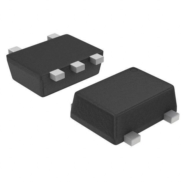
| 产品图片 |
|
| rohs | 符合RoHS无铅 / 符合限制有害物质指令(RoHS)规范要求 |
| 产品系列 | 电源管理 IC,低压差稳压器,Texas Instruments TPS78227DDCR- |
| 数据手册 | |
| 产品型号 | TPS78227DDCR |
| 产品目录页面 | |
| 产品种类 | 低压差稳压器 |
| 供应商器件封装 | 5-SOT |
| 其它名称 | 296-23825-6 |
| 制造商产品页 | http://www.ti.com/general/docs/suppproductinfo.tsp?distId=10&orderablePartNumber=TPS78227DDCR |
| 包装 | Digi-Reel® |
| 商标 | Texas Instruments |
| 回动电压—最大值 | 250 mV at 150 mA |
| 安装类型 | 表面贴装 |
| 安装风格 | SMD/SMT |
| 封装 | Reel |
| 封装/外壳 | SOT-23-5 细型,TSOT-23-5 |
| 封装/箱体 | SOT-23-5 |
| 工作温度 | -40°C ~ 125°C |
| 工厂包装数量 | 3000 |
| 最大功率耗散 | 0.5 W |
| 最大工作温度 | + 125 C |
| 最大输入电压 | 5.5 V |
| 最小工作温度 | - 40 C |
| 最小输入电压 | + 2.2 V |
| 标准包装 | 1 |
| 电压-跌落(典型值) | 0.13V @ 150mA |
| 电压-输入 | 最高 5.5V |
| 电压-输出 | 2.7V |
| 电压调节准确度 | 1 % |
| 电流-输出 | 150mA |
| 电流-限制(最小值) | 150mA |
| 稳压器拓扑 | 正,固定式 |
| 稳压器数 | 1 |
| 系列 | TPS78227 |
| 线路调整率 | 0.01 |
| 负载调节 | 2 % |
| 输出电压 | 2.7 V |
| 输出电流 | 150 mA |
| 输出端数量 | 1 Output |
| 输出类型 | Fixed |


- 商务部:美国ITC正式对集成电路等产品启动337调查
- 曝三星4nm工艺存在良率问题 高通将骁龙8 Gen1或转产台积电
- 太阳诱电将投资9.5亿元在常州建新厂生产MLCC 预计2023年完工
- 英特尔发布欧洲新工厂建设计划 深化IDM 2.0 战略
- 台积电先进制程称霸业界 有大客户加持明年业绩稳了
- 达到5530亿美元!SIA预计今年全球半导体销售额将创下新高
- 英特尔拟将自动驾驶子公司Mobileye上市 估值或超500亿美元
- 三星加码芯片和SET,合并消费电子和移动部门,撤换高东真等 CEO
- 三星电子宣布重大人事变动 还合并消费电子和移动部门
- 海关总署:前11个月进口集成电路产品价值2.52万亿元 增长14.8%


PDF Datasheet 数据手册内容提取
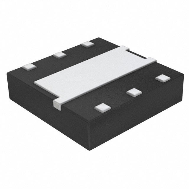
Product Sample & Technical Tools & Support & Reference Folder Buy Documents Software Community Design TPS782 SBVS115D–AUGUST2008–REVISEDJANUARY2015 TPS782 500-nA I ,150-mA, Ultra-Low Quiescent Current Q Low-Dropout Linear Regulator 1 Features 3 Description • LowI :500nA The TPS782 family of low-dropout regulators (LDOs) 1 Q offers the benefits of ultra-low power and miniaturized • 150-mA,Low-DropoutRegulator packaging. • InputVoltageRange:2.2Vto5.5V This LDO is designed specifically for battery-powered • Low-Dropoutat25°C,130mVat150mA applications where ultra-low quiescent current is a • Low-Dropoutat85°C,175mVat150mA critical parameter. The TPS782, with ultra-low I (500 Q • 3%AccuracyOverLoad,Line,andTemperature nA), is ideal for microprocessors, microcontrollers, andotherbattery-poweredapplications. • Stablewitha1.0-μFCeramicCapacitor • ThermalShutdownandOvercurrentProtection The ultra-low power and miniaturized packaging allow designers to customize power consumption for • CMOSLogicLevel-CompatibleEnablePin specificapplications. • AvailableinDDC(TSOT23-5)orDRV(2-mmx2- The TPS782 family is designed to be compatible with mmSON-6)Packages the TI MSP430 and other similar products. The enable pin (EN) is compatible with standard CMOS 2 Applications logic. This device allows for minimal board space • TIMSP430AttachApplications because of miniaturized packaging and a potentially small output capacitor. The TPS782 series also • WirelessHandsetsandSmartPhones features thermal shutdown and current limit to protect • MP3Players the device during fault conditions. All packages have • Battery-OperatedHandheldProducts an operating temperature range of T = –40°C to J 125°C. Forhigh-performanceapplicationsthatrequireadual- level voltage option, consider the TPS780 series, with anI of500nAanddynamicvoltagescaling. Q DeviceInformation(1) PARTNUMBER PACKAGE BODYSIZE(NOM) SOT(5) 2.90mmx1.60mm TPS782 SON(6) 2.00mmx2.00mm (1) For all available packages, see the orderable addendum at theendofthedatasheet. SimplifiedSchematic VIN IN OUT VOUT 1mF 1mF TPS782xx On Off EN GND 1 An IMPORTANT NOTICE at the end of this data sheet addresses availability, warranty, changes, use in safety-critical applications, intellectualpropertymattersandotherimportantdisclaimers.PRODUCTIONDATA.
TPS782 SBVS115D–AUGUST2008–REVISEDJANUARY2015 www.ti.com Table of Contents 1 Features.................................................................. 1 8 ApplicationandImplementation........................ 12 2 Applications........................................................... 1 8.1 ApplicationInformation............................................12 3 Description............................................................. 1 8.2 TypicalApplication..................................................12 4 RevisionHistory..................................................... 2 8.3 Do'sandDon’ts.......................................................13 5 PinConfigurationandFunctions......................... 3 9 PowerSupplyRecommendations...................... 13 6 Specifications......................................................... 4 10 Layout................................................................... 14 6.1 AbsoluteMaximumRatings......................................4 10.1 LayoutGuidelines.................................................14 6.2 ESDRatings ............................................................4 10.2 LayoutExample....................................................14 6.3 RecommendedOperatingConditions.......................4 10.3 ThermalProtection................................................14 6.4 ThermalInformation..................................................4 10.4 PowerDissipation.................................................14 6.5 ElectricalCharacteristics...........................................5 11 DeviceandDocumentationSupport................. 15 6.6 TypicalCharacteristics..............................................6 11.1 DeviceSupport......................................................15 7 DetailedDescription............................................ 10 11.2 DocumentationSupport .......................................15 7.1 Overview.................................................................10 11.3 Trademarks...........................................................15 7.2 FunctionalBlockDiagram.......................................10 11.4 ElectrostaticDischargeCaution............................15 7.3 FeatureDescription.................................................10 11.5 Glossary................................................................15 7.4 DeviceFunctionalModes........................................11 12 Mechanical,Packaging,andOrderable Information........................................................... 15 4 Revision History NOTE:Pagenumbersforpreviousrevisionsmaydifferfrompagenumbersinthecurrentversion. ChangesfromRevisionC(January2014)toRevisionD Page • AddedESDRatingstable,ThermalInformationtable,FeatureDescriptionsection,DeviceFunctionalModes, ApplicationandImplementationsection,PowerSupplyRecommendationssection,Layoutsection,Deviceand DocumentationSupportsection,andMechanical,Packaging,andOrderableInformationsection ..................................... 1 • Changeddocumentformattolatestdatasheetstandards;movedexistingsections............................................................ 1 • Changedfactoryprogrammingfeaturebullet ........................................................................................................................ 1 • Addedinputvoltagerangefeaturebullet............................................................................................................................... 1 • ChangedApplicationslist ...................................................................................................................................................... 1 • ChangedDescriptionsectiontext(allparagraphs)................................................................................................................ 1 • Addedsimplifiedschematictofrontpage.............................................................................................................................. 1 • Deletedfootnotesfrompinconfigurationdrawings ............................................................................................................... 3 • ChangedpindescriptionsthroughoutPinFunctionstable .................................................................................................... 3 • ChangedoperatingjunctiontemperaturerangemaximumvalueinAbsoluteMaximumRatingstable................................. 4 • DeletedDissipationRatingstable;seeThermalInformationtable......................................................................................... 4 • ChangedsymbolandparameternamesforclarityinElectricalCharacteristicstable .......................................................... 5 ChangesfromRevisionB(May2010)toRevisionC Page • ChangedI valueinDescriptionsectionfrom1µAto500nA.............................................................................................. 1 Q ChangesfromRevisionA(September2008)toRevisionB Page • ChangedfirstbulletofFeatureslist........................................................................................................................................ 1 • Updatedtitleofdatasheet...................................................................................................................................................... 1 • Changedgroundpincurrent,I =0mAtypicalspecificationfrom1.0μAto0.42μA......................................................... 5 OUT • AddedFigure6 ...................................................................................................................................................................... 6 2 SubmitDocumentationFeedback Copyright©2008–2015,TexasInstrumentsIncorporated ProductFolderLinks:TPS782
TPS782 www.ti.com SBVS115D–AUGUST2008–REVISEDJANUARY2015 5 Pin Configuration and Functions DDCPACKAGE TSOT23-5 (TOPVIEW) IN 1 5 OUT GND 2 EN 3 4 GND DRVPACKAGE 2-mmx2-mmSON-6 (TOPVIEW) OUT 1 6 IN Thermal N/C 2 Pad 5 GND GND 3 4 EN PinFunctions PIN I/O DESCRIPTION NAME DRV DDC Regulatedoutputvoltagepin.Asmall(1-μF)ceramiccapacitorisneededfromthispinto OUT 1 5 O groundtoassurestability.SeetheInputandOutputCapacitorRequirementsinthe ApplicationandImplementationsectionformoredetails. NC 2 — — Nointernalconnection. Enablepin.Drivethispinover1.2Vtoturnontheregulator.Drivethispinbelow0.4Vto EN 4 3 I puttheregulatorintoshutdownmode,reducingoperatingcurrentto18nAtypical. GND 3,5 2,4 — Groundpin.Tieallgroundpinstogroundforproperoperation. Inputpin.Forstableoperation,placeasmall,0.1-µFcapacitorfromthispintoground; IN 6 1 I typicalinputcapacitor=1.0µF.Tiebackbothinputandoutputcapacitorgroundstothe ICground,withnosignificantimpedancebetweenthem. Thermal Thermal — — Connectthethermalpadtoground. pad pad Copyright©2008–2015,TexasInstrumentsIncorporated SubmitDocumentationFeedback 3 ProductFolderLinks:TPS782
TPS782 SBVS115D–AUGUST2008–REVISEDJANUARY2015 www.ti.com 6 Specifications 6.1 Absolute Maximum Ratings overoperatingfree-airtemperaturerange(unlessotherwisenoted) (1) MIN MAX UNIT Inputvoltagerange –0.3 6 V Voltage Enable –0.3 V +0.3 V IN Outputvoltagerange –0.3 V +0.3 V IN Current Maximumoutputcurrent Internallylimited A Outputshort-circuitduration Indefinite Totalcontinuouspowerdissipation,P SeeThermalInformation DISS Operatingjunctiontemperature,T –40 160 °C J Storagetemperature,T –55 150 °C stg (1) StressesbeyondthoselistedunderAbsoluteMaximumRatingsmaycausepermanentdamagetothedevice.Thesearestressratings only,whichdonotimplyfunctionaloperationofthedeviceattheseoranyotherconditionsbeyondthoseindicatedunderRecommended OperatingConditions.Exposuretoabsolute-maximum-ratedconditionsforextendedperiodsmayaffectdevicereliability. 6.2 ESD Ratings VALUE UNIT Humanbodymodel(HBM),perANSI/ESDA/JEDECJS-001,allpins(1) ±2000 V(ESD) Electrostaticdischarge Chargeddevicemodel(CDM),perJEDECspecificationJESD22-C101, V allpins(2) ±500 (1) JEDECdocumentJEP155statesthat500-VHBMallowssafemanufacturingwithastandardESDcontrolprocess. (2) JEDECdocumentJEP157statesthat250-VCDMallowssafemanufacturingwithastandardESDcontrolprocess. 6.3 Recommended Operating Conditions overoperatingfree-airtemperaturerange(unlessotherwisenoted) MIN NOM MAX UNIT V Inputvoltage 2.2 5.5 V IN V Outputvoltage 1.8 4.2 V OUT V Enablevoltage 0 V V EN IN I Outputcurrent 0 150 mA OUT T Junctiontemperature –40 125 °C J 6.4 Thermal Information TPS782 THERMALMETRIC(1) DRV DDC UNIT 6PINS 5PINS R Junction-to-ambientthermalresistance 65.9 193.0 θJA R Junction-to-case(top)thermalresistance 87.3 40.1 θJC(top) R Junction-to-boardthermalresistance 35.4 34.3 θJB °C/W ψ Junction-to-topcharacterizationparameter 1.7 0.9 JT ψ Junction-to-boardcharacterizationparameter 35.8 34.1 JB R Junction-to-case(bottom)thermalresistance 6.1 — θJC(bot) (1) Formoreinformationabouttraditionalandnewthermalmetrics,seetheICPackageThermalMetricsapplicationreport,SPRA953. 4 SubmitDocumentationFeedback Copyright©2008–2015,TexasInstrumentsIncorporated ProductFolderLinks:TPS782
TPS782 www.ti.com SBVS115D–AUGUST2008–REVISEDJANUARY2015 6.5 Electrical Characteristics Overoperatingtemperaturerange(T =–40°Cto125°C),V =V +0.5Vor2.2V,whicheverisgreater; J IN OUT(nom) I =100μA,V =V ,C =1.0μF,fixedV testconditions,unlessotherwisenoted.TypicalvaluesatT =25°C. OUT EN IN OUT OUT J PARAMETER TESTCONDITIONS MIN TYP MAX UNIT V Inputvoltagerange 2.2 5.5 V IN Nominal T =25°C –2% ±1% +2% J VOUT DCoutputaccuracy OverVIN,IOUT, VOUT(nom)+0.5V≤VIN≤5.5V, –3% ±2% 3% temperature 0mA≤I ≤150mA OUT V +0.5V≤V ≤5.5V, ΔV Lineregulation OUT(nom) IN ±1% OUT(ΔVIN) I =5mA OUT ΔV Loadregulation 0mA≤I ≤150mA ±2% OUT(ΔIOUT) OUT V Dropoutvoltage(1) V =95%V ,I =150mA 130 250 mV DO IN OUT(nom) OUT I Outputcurrentlimit V =0.90×V 150 230 400 mA LIM OUT OUT(nom) I =0mA 0.42 1.3 μA OUT I Groundpincurrent GND I =150mA 8 μA OUT I ENpincurrent V =5.5V 40 nA EN EN V ≤0.4V,2.2V≤V <5.5V, I Shutdowncurrent(I ) EN IN 18 130 nA SHDN GND T =–40°Cto100°C J f=10Hz 40 dB V =4.3V, IN PSRR Power-supplyrejectionratio V =3.3V, f=100Hz 20 dB OUT I =150mA OUT f=1kHz 15 dB BW=100Hzto100kHz,V =3.2V, V Outputnoisevoltage IN 108 μV n V =2.7V,I =1mA RMS OUT OUT t Startuptime(2) COUT=1.0μF,VOUT=10%VOUT(nom)to 500 μs STR V =90%V OUT OUT(nom) I =150mA,C =1.0μF, OUT OUT t Shutdowntime(3) VOUT=2.8V, 500(4) μs SHDN V =90%V to OUT OUT(nom) V =10%V OUT OUT(nom) Shutdown,temperatureincreasing 160 °C T Thermalshutdowntemperature sd Reset,temperaturedecreasing 140 °C T Operatingjunctiontemperature –40 125 °C J (1) V isnotmeasuredfordeviceswithV ≤2.3VbecauseminimumV =2.2V. DO OUT(nom) IN (2) TimefromV =1.2VtoV =90%(V ). EN OUT OUT(nom) (3) TimefromV =0.4VtoV =10%(V ). EN OUT OUT(nom) (4) SeeShutdownintheFeatureDescriptionsectionformoredetails. Copyright©2008–2015,TexasInstrumentsIncorporated SubmitDocumentationFeedback 5 ProductFolderLinks:TPS782
TPS782 SBVS115D–AUGUST2008–REVISEDJANUARY2015 www.ti.com 6.6 Typical Characteristics OvertheoperatingtemperaturerangeofT =–40°Cto125°C,V =V +0.5Vor2.2V,whicheverisgreater;I J IN OUT(nom) OUT =100μA,V =V ,C =1μF,andC =1μF,unlessotherwisenoted. EN IN OUT IN 1.0 3 0.8 0.6 TJ=-40°C 2 T = +25°C J 0.4 1 %) 0.2 %) TJ=-40°C (UT 0 (UT 0 VO -0.2 VO -0.4 TJ= +85°C -1 -0.6 -2 -0.8 TJ= +85°C TJ= +25°C -1.0 -3 3.8 4.0 4.2 4.4 4.6 4.8 5.0 5.2 5.4 5.6 3.8 4.0 4.2 4.4 4.6 4.8 5.0 5.2 5.4 5.6 V (V) V (V) IN IN Figure1.LineRegulation,I =5mA,TPS78227 Figure2.LineRegulation,I =150mA,TPS78227 OUT OUT 3 250 T = +125°C 2 J 200 %) 1 TJ=-40°C ) (mV)UT 150 TJ= +85°C V(OUT 0 -VVINO 100 -1 ( O -2 TJ= +25°C TJ= +85°C VD 50 TJ= +25°C TJ=-40°C -3 0 0 25 50 75 100 125 150 0 25 50 75 100 125 150 I (mA) I (mA) OUT OUT Figure3.LoadRegulation,V =3.8V,TPS78227 Figure4. DropoutVoltagevsOutputCurrent,V =0.95× IN IN V ,TPS78227 OUT(nom) 250 900 800 V) 200 150mA 700 T = +85°C TJ= +125°C m J V) (OUT 150 100mA (nA) 650000 TJ= +25°C -VIN 100 IGND400 ( 300 VDO 50 50mA 200 TJ=-40°C 10mA 100 0 0 -40 -25 -10 5 20 35 50 65 80 95 110 125 3.8 4.0 4.2 4.4 4.6 4.8 5.0 5.2 5.4 5.6 TJ(°C) VIN(V) Figure5. DropoutVoltagevsJunctionTemperature,VIN= Figure6.GroundPinCurrentvsInputVoltage,IOUT=0mA, 0.95×VOUT(nom),TPS78227 TPS78233 6 SubmitDocumentationFeedback Copyright©2008–2015,TexasInstrumentsIncorporated ProductFolderLinks:TPS782
TPS782 www.ti.com SBVS115D–AUGUST2008–REVISEDJANUARY2015 Typical Characteristics (continued) OvertheoperatingtemperaturerangeofT =–40°Cto125°C,V =V +0.5Vor2.2V,whicheverisgreater;I J IN OUT(nom) OUT =100μA,V =V ,C =1μF,andC =1μF,unlessotherwisenoted. EN IN OUT IN 6 3 5 2 TJ= +85°C TJ= +125°C 4 1 T =-40°C A) %) J (mD 3 (UT 0 N O G V I 2 -1 T = +25°C J T =-40°C J 1 -2 T = +85°C T = +25°C J J 0 -3 3.8 4.0 4.2 4.4 4.6 4.8 5.0 5.2 5.4 5.6 3.8 4.0 4.2 4.4 4.6 4.8 5.0 5.2 5.4 5.6 V (V) V (V) IN IN Figure7. GroundPinCurrentvsInputVoltage,I =50 Figure8. GroundPinCurrentvsInputVoltage,I =150 OUT OUT mA,TPS78227 mA,TPS78227 300 2.0 290 1.8 280 1.6 mA) 270 TJ=-40°C 1.4 TJ=-40°C ent Limit ( 222654000 TJ= +25°C I(nA)EN 110...208 TJ= +85°C TJ= +25°C Curr 230 TJ= +85°C 0.6 220 0.4 T = +125°C J 210 0.2 200 0 3.8 4.0 4.2 4.4 4.6 4.8 5.0 5.2 5.4 5.6 3.8 4.0 4.2 4.4 4.6 4.8 5.0 5.2 5.4 5.6 V (V) V (V) IN IN Figure9. CurrentLimitvsInputVoltage,V =95% Figure10. EnablePinCurrentvsInputVoltage,I =100 OUT OUT V ,TPS78227 μA,TPS78227 OUT(nom) 1.2 1 1.1 0.1mA 1.0 VENOn 0 0.9 V) (V)N 0.8 (OUT 5mA E V V D 0.7 % V Off -1 0.6 EN 150mA 0.5 0.4 -2 -40 -25 -10 5 20 35 50 65 80 95 110 125 -40 -25 -10 5 20 35 50 65 80 95 110 125 T (°C) T (°C) J J Figure11. EnablePinHysteresisvsJunctionTemperature, Figure12. %ΔV vsJunctionTemperature,V =3.3V, OUT IN I =1mA,TPS78227 TPS78227 OUT Copyright©2008–2015,TexasInstrumentsIncorporated SubmitDocumentationFeedback 7 ProductFolderLinks:TPS782
TPS782 SBVS115D–AUGUST2008–REVISEDJANUARY2015 www.ti.com Typical Characteristics (continued) OvertheoperatingtemperaturerangeofT =–40°Cto125°C,V =V +0.5Vor2.2V,whicheverisgreater;I J IN OUT(nom) OUT =100μA,V =V ,C =1μF,andC =1μF,unlessotherwisenoted. EN IN OUT IN 3 100 )z H Ö 2 V/ m 10 D%V(V)OUT --1012 150m5AmA0.1mA put Spectral Noise Density ( 0.00.111 105910mmmVAARMS 10195m0VmRAMS -3 Out 0.001 108mVRMS -40 -25 -10 5 20 35 50 65 80 95 110 125 10 100 1k 10k 100k T (°C) Frequency (Hz) J Figure13. %ΔV vsJunctionTemperature,V =3.7V, Figure14. OutputSpectralNoiseDensityvsFrequency,C OUT IN IN TPS78227 =1μF,C =2.2μF,V =3.2V,TPS78227 OUT IN 80 1mA VIN VIN= 0.0V to5.0V 70 V VOUT= 3.3V 60 V/div) Enable OUT ICOOUUTT== 1 1500mmFA Cu SRR (dB) 5400 50mA Voltage (1 Load Current rrent (50mA P 30 /d iv 20 0V ) 150mA 10 0 10 100 1k 10k 100k 1M 10M Time (20ms/div) Frequency (Hz) Figure16. InputVoltageRampvsOutputVoltage, Figure15. RippleRejectionvsFrequency,V =4.2V,V TPS78233 IN OUT =2.7V,C =2.2μF,TPS78227 OUT VIN Enable v) v) V/di VOUT Load Current Cu V/di V Cu Voltage (1 V = 5.5V rrent (50m Voltage (1 Load Current IN rrent (50m IN A A VIOOUUTT== 1 35.03mVA /div) VIN= 0.0V to 5.5V /div) 0V COUT= 10mF 00AV VOUT VICOOUUTT=== 1 210.002mmVFA OUT Time (20ms/div) Time (1ms/div) Figure17. OutputVoltagevsEnable(SlowRamp), Figure18. InputVoltagevsDelaytoOutput,TPS78222 TPS78233 8 SubmitDocumentationFeedback Copyright©2008–2015,TexasInstrumentsIncorporated ProductFolderLinks:TPS782
TPS782 www.ti.com SBVS115D–AUGUST2008–REVISEDJANUARY2015 Typical Characteristics (continued) OvertheoperatingtemperaturerangeofT =–40°Cto125°C,V =V +0.5Vor2.2V,whicheverisgreater;I J IN OUT(nom) OUT =100μA,V =V ,C =1μF,andC =1μF,unlessotherwisenoted. EN IN OUT IN Enable V Enable v) IN edi Voltag(100mV/ VVIOIOUNUT=T= =5 0 .35m.V3AV to 10mA VOUT Load (10mCu Voltage (1V/div) VIN LVoOaUdT Current Current (50mA COUT= 10mF Current A/div)rrent 0V VVIONU=T =5 .35.03VV /div) 0A IOUT= 150mA C = 10mF OUT Time (5ms/div) Time (1ms/div) Figure19.LoadTransientResponse,TPS78233 Figure20. EnablePinvsOutputVoltageResponseand OutputCurrent,TPS78233 V = 5.5V IN e (1V/div) VIN Enable VOUT VICOOOUUUTTT=== 1 315.003mmVFA Curren Voltag Load t (50m Current A/d iv 0V ) Time (1ms/div) Figure21. EnablePinvsOutputVoltageDelay,TPS78233 Copyright©2008–2015,TexasInstrumentsIncorporated SubmitDocumentationFeedback 9 ProductFolderLinks:TPS782
TPS782 SBVS115D–AUGUST2008–REVISEDJANUARY2015 www.ti.com 7 Detailed Description 7.1 Overview The TPS782 family of low-dropout regulators (LDOs) is designed specifically for battery-powered applications where ultralow quiescent current is a critical parameter. The TPS782 family is compatible with the TI MSP430 and other similar products. The enable pin (EN) is compatible with standard CMOS logic. This LDO family is stablewithanyoutputcapacitorgreaterthan1.0µF. 7.2 Functional Block Diagram IN OUT Current Limit Thermal Shutdown x EPROM u M EN Bandgap Active Pull- 10kW Down Logic GND 7.3 Feature Description 7.3.1 InternalCurrentLimit The TPS782 is internally current-limited to protect the regulator during fault conditions. During current limit, the output sources a fixed amount of current that is largely independent of output voltage. For reliable operation, the deviceshouldnotbeoperatedinacurrentlimitstateforextendedperiodsoftime. The PMOS pass element in the TPS782 series has a built-in body diode that conducts current when the voltage at OUT exceeds the voltage at IN. This current is not limited, so if extended reverse voltage operation is anticipated,externallimitingto5%ofratedoutputcurrentmaybeappropriate. 7.3.2 ActiveV Pulldown OUT In the TPS782 series, the active pulldown discharges V when the device is off. However, the input voltage OUT mustbegreaterthan2.2Vfortheactivepulldowntowork. 10 SubmitDocumentationFeedback Copyright©2008–2015,TexasInstrumentsIncorporated ProductFolderLinks:TPS782
TPS782 www.ti.com SBVS115D–AUGUST2008–REVISEDJANUARY2015 Feature Description (continued) 7.3.3 Shutdown The enable pin (EN) is active high and is compatible with standard and low-voltage CMOS levels. When shutdown capability is not required, EN should be connected to the IN pin, as shown in Figure 22. The TPS782 series, with internal active output pulldown circuitry, discharges the output to within 5% V with a time (t) OUT showninEquation1: 10kW´R t = 3 L ´C 10kW+ R OUT L (1) Where: R =outputloadresistance L C =outputcapacitance OUT 4.2V to 5.5V 2.7V VIN IN OUT VOUT 1mF 1mF TPS78227 EN GND Figure22. CircuitShowingENTiedHighWhenShutdownCapabilityIsNotRequired 7.4 Device Functional Modes Table1providesaquickcomparisonbetweenthenormal,dropout,anddisabledmodesofoperation. Table1.DeviceFunctionalModeComparison PARAMETER OPERATINGMODE V EN I T IN OUT J Normal V >V +V V >V I <I T <T IN OUT(nom) DO EN EN(HI) OUT LIM J SD Dropout V <V +V V >V I <I T <T IN OUT(nom) DO EN EN(HI) OUT LIM J SD Disabled — V <V — T >T EN EN(LO) J SD 7.4.1 NormalOperation Thedeviceregulatestothenominaloutputvoltageunderthefollowingconditions: • Theinputvoltageisgreaterthanthenominaloutputvoltageplusthedropoutvoltage(V +V ). OUT(nom) DO • The enable voltage has previously exceeded the enable rising threshold voltage and not yet decreased below theenablefallingthreshold. • Theoutputcurrentislessthanthecurrentlimit(I <I ). OUT LIM • Thedevicejunctiontemperatureislessthanthethermalshutdowntemperature(T <T ). J SD 7.4.2 DropoutOperation If the input voltage is lower than the nominal output voltage plus the specified dropout voltage, but all other conditions are met for normal operation, the device operates in dropout mode. In this mode, the output voltage tracks the input voltage. During this mode, the transient performance of the device becomes significantly degraded because the pass device is in a triode state and no longer controls the current through the LDO. Line orloadtransientsindropoutcanresultinlargeoutput-voltagedeviations. Copyright©2008–2015,TexasInstrumentsIncorporated SubmitDocumentationFeedback 11 ProductFolderLinks:TPS782
TPS782 SBVS115D–AUGUST2008–REVISEDJANUARY2015 www.ti.com 7.4.3 Disabled Thedeviceisdisabledunderthefollowingconditions: • The enable voltage is less than the enable falling threshold voltage or has not yet exceeded the enable rising threshold. • Thedevicejunctiontemperatureisgreaterthanthethermalshutdowntemperature(T >T ). J SD 8 Application and Implementation NOTE Information in the following applications sections is not part of the TI component specification, and TI does not warrant its accuracy or completeness. TI’s customers are responsible for determining suitability of components for their purposes. Customers should validateandtesttheirdesignimplementationtoconfirmsystemfunctionality. 8.1 Application Information The TPS782 family of LDOs is factory-programmable to have a fixed output. Note that during startup or steady- stateconditions,itisimportantthattheENpinvoltageneverexceedV +0.3V. IN 8.2 Typical Application VIN IN OUT VOUT 1mF 1mF TPS782xx On Off EN GND Figure23. TypicalApplicationCircuit 8.2.1 DesignRequirements Selectthedesireddevicebasedontheoutputvoltage. Provide an input supply with adequate headroom to account for dropout and output current to account for the GNDpincurrent,andpowertheload.Selectinputandoutputcapacitorsbasedonapplicationneeds. 8.2.2 DetailedDesignProcedure 8.2.2.1 InputandOutputCapacitorRequirements Although an input capacitor is not required for stability, it is good analog design practice to connect a 0.1-μF to 1.0-μF low equivalent series resistance (ESR) capacitor across the input supply near the regulator. This capacitor counteracts reactive input sources and improves transient response, noise rejection, and ripple rejection. A higher-value capacitor may be necessary if large, fast rise-time load transients are anticipated, or if the device is not located near the power source. If source impedance is not sufficiently low, a 0.1-μF input capacitormaybenecessarytoensurestability. The TPS782 series is designed to be stable with standard ceramic capacitors with values of 1.0 μF or larger at the output. X5R- and X7R-type capacitors are best because they have minimal variation in value and ESR over temperature. Maximum ESR should be less than 1.0 Ω. With tolerance and dc bias effects, the minimum capacitancetoensurestabilityis1μF. 12 SubmitDocumentationFeedback Copyright©2008–2015,TexasInstrumentsIncorporated ProductFolderLinks:TPS782
TPS782 www.ti.com SBVS115D–AUGUST2008–REVISEDJANUARY2015 Typical Application (continued) 8.2.2.2 DropoutVoltage The TPS782 uses a PMOS pass transistor to achieve low dropout. When (V – V ) is less than the dropout IN OUT voltage (V ), the PMOS pass device is the linear region of operation and the input-to-output resistance is the DO R of the PMOS pass element. V approximately scales with output current because the PMOS device DS(ON) DO behaves like a resistor in dropout. As with any linear regulator, PSRR and transient response are degraded as (V – V ) approaches dropout. This effect is shown in the Typical Characteristics section. Refer to application IN OUT reportSLVA207,UnderstandingLDODropout,availablefordownloadfromwww.ti.com. 8.2.2.3 TransientResponse As with any regulator, increasing the size of the output capacitor reduces over/undershoot magnitude but increasesdurationofthetransientresponse.Formoreinformation,seeFigure19. 8.2.2.4 MinimumLoad TheTPS782seriesisstablewithnooutputload.TraditionalPMOSLDOregulatorssufferfromlowerloopgainat very light output loads. The TPS782 employs an innovative, low-current circuit under very light or no-load conditions, resulting in improved output voltage regulation performance down to zero output current. See Figure19fortheloadtransientresponse. 8.2.3 ApplicationCurves 100 80 )Hz 1mA ÖV/ 70 m 10 Density ( 1 10195m0VmRAMS B) 6500 al Noise 0.1 PSRR (d 4300 50mA ctr 50mA Spe 0.01 109mVRMS 20 150mA put 1mA 10 ut 108mV O RMS 0.001 0 10 100 1k 10k 100k 10 100 1k 10k 100k 1M 10M Frequency (Hz) Frequency (Hz) Figure24.OutputSpectralNoiseDensityvsFrequency, Figure25.RippleRejectionvsFrequency,V =4.2V, IN CIN=1μF,COUT=2.2μF,VIN=3.2V,TPS78227 VOUT=2.7V,COUT=2.2μF,TPS78227 8.3 Do's and Don’ts Doplaceatleastone1-µFceramiccapacitorascloseaspossibletotheOUTpinoftheregulator. Donotplacetheoutputcapacitormorethan10mmawayfromtheregulator. Do connect a 0.1-μF to 1.0-μF low equivalent series resistance (ESR) capacitor across the IN pin and GND of theregulator. Donotexceedtheabsolutemaximumratings. 9 Power Supply Recommendations For best performance, connect a low-output impedance power supply directly to the IN pin of the TPS782 series. Inductive impedances between the input supply and the IN pin create significant voltage excursions at the IN pin duringstartuporloadtransientevents.Ifinductiveimpedancesareunavoidable,useaninputcapacitor. Copyright©2008–2015,TexasInstrumentsIncorporated SubmitDocumentationFeedback 13 ProductFolderLinks:TPS782
TPS782 SBVS115D–AUGUST2008–REVISEDJANUARY2015 www.ti.com 10 Layout 10.1 Layout Guidelines To improve ac performance (such as PSRR, output noise, and transient response), it is recommended that the printed circuit board (PCB) be designed with separate ground planes for V and V , with each ground plane IN OUT connected only at the GND pin of the device. In addition, the ground connection for the output capacitor should connectdirectlytotheGNDpinofthedevice.HighESRcapacitorsmaydegradePSRR. 10.2 Layout Example V V IN OUT 1 5 CIN 2 COUT 3 4 GND PLANE Represents via used for application-specific connections Figure26. LayoutExampleforDDCPackage 10.3 Thermal Protection Thermal protection disables the device output when the junction temperature rises to approximately 160°C, allowing the device to cool. Once the junction temperature cools to approximately 140°C, the output circuitry is enabled. Depending on power dissipation, thermal resistance, and ambient temperature, the thermal protection circuit may cycle on and off again. This cycling limits the dissipation of the regulator, protecting it from damage asaresultofoverheating. Any tendency to activate the thermal protection circuit indicates excessive power dissipation or an inadequate heatsink. For reliable operation, junction temperature should be limited to 125°C maximum. To estimate the margin of safety in a complete design (including heatsink), increase the ambient temperature until the thermal protection is triggered; use worst-case loads and signal conditions. For good reliability, thermal protection should trigger at least 35°C above the maximum expected ambient condition of your particular application. This configuration produces a worst-case junction temperature of 125°C at the highest expected ambient temperature andworst-caseload. The internal protection circuitry of the TPS782 series has been designed to protect against overload conditions. However, it is not intended to replace proper heatsinking. Continuously running the TPS782 series into thermal shutdowndegradesdevicereliability. 10.4 Power Dissipation The ability to remove heat from the die is different for each package type, presenting different considerations in the PCB layout. The PCB area around the device that is free of other components moves the heat from the device to the ambient air. Performance data for JEDEC low- and high-K boards are given in the Thermal Information table. Using heavier copper increases the effectiveness in removing heat from the device. The addition of plated through-holes to heat-dissipating layers also improves the heatsink effectiveness. Power dissipation depends on input voltage and load conditions. Power dissipation (P ) is equal to the product of the D outputcurrenttimesthevoltagedropacrosstheoutputpasselement(V toV ),asshowninEquation2: IN OUT P = (V -V )´I D IN OUT OUT (2) 14 SubmitDocumentationFeedback Copyright©2008–2015,TexasInstrumentsIncorporated ProductFolderLinks:TPS782
TPS782 www.ti.com SBVS115D–AUGUST2008–REVISEDJANUARY2015 11 Device and Documentation Support 11.1 Device Support 11.1.1 DevelopmentSupport 11.1.1.1 EvaluationModules An evaluation module (EVM) is available to assist in the initial circuit performance evaluation using the TPS782. The TPS782xxEVM evaluation modules (and related user guide) can be requested at the Texas Instruments websitethroughtheproductfoldersorpurchaseddirectlyfromtheTIeStore. 11.1.1.2 SpiceModels Computer simulation of circuit performance using SPICE is often useful when analyzing the performance of analogcircuitsandsystems.ASPICEmodelfortheTPS782familyisavailablethroughtheproductfoldersunder SimulationModels. 11.1.2 DeviceNomenclature Table2.DeviceNomenclature(1) PRODUCT V OUT TPS782xxyyyz XXisthenominaloutputvoltage YYYisthepackagedesignator. Zisthetapeandreelquantity(R=3000,T=250). (1) ForthemostcurrentpackageandorderinginformationseethePackageOptionAddendumattheendofthisdocument,orseetheTI websiteatwww.ti.com. 11.2 Documentation Support 11.2.1 RelatedDocumentation Forrelateddocumentationseethefollowing: • Applicationreport. UnderstandingLDODropout,SLVA207 • Productinformation. Low-powerMCUs,MSP430 • Referencedesign.WaterMeterImplementationwithFRAMMicrocontroller,TIDU517 11.3 Trademarks Alltrademarksarethepropertyoftheirrespectiveowners. 11.4 Electrostatic Discharge Caution Thesedeviceshavelimitedbuilt-inESDprotection.Theleadsshouldbeshortedtogetherorthedeviceplacedinconductivefoam duringstorageorhandlingtopreventelectrostaticdamagetotheMOSgates. 11.5 Glossary SLYZ022—TIGlossary. Thisglossarylistsandexplainsterms,acronyms,anddefinitions. 12 Mechanical, Packaging, and Orderable Information The following pages include mechanical, packaging, and orderable information. This information is the most current data available for the designated devices. This data is subject to change without notice and revision of thisdocument.Forbrowser-basedversionsofthisdatasheet,refertotheleft-handnavigation. Copyright©2008–2015,TexasInstrumentsIncorporated SubmitDocumentationFeedback 15 ProductFolderLinks:TPS782
PACKAGE OPTION ADDENDUM www.ti.com 6-Feb-2020 PACKAGING INFORMATION Orderable Device Status Package Type Package Pins Package Eco Plan Lead/Ball Finish MSL Peak Temp Op Temp (°C) Device Marking Samples (1) Drawing Qty (2) (6) (3) (4/5) TPS78218DDCR ACTIVE SOT-23-THIN DDC 5 3000 Green (RoHS NIPDAU Level-2-260C-1 YEAR -40 to 125 SJY & no Sb/Br) TPS78218DDCT ACTIVE SOT-23-THIN DDC 5 250 Green (RoHS NIPDAU Level-2-260C-1 YEAR -40 to 125 SJY & no Sb/Br) TPS78218DRVR ACTIVE WSON DRV 6 3000 Green (RoHS NIPDAU Level-1-260C-UNLIM -40 to 125 SAF & no Sb/Br) TPS78218DRVT ACTIVE WSON DRV 6 250 Green (RoHS NIPDAU Level-1-260C-UNLIM -40 to 125 SAF & no Sb/Br) TPS78222DRVR ACTIVE WSON DRV 6 3000 Green (RoHS NIPDAU Level-1-260C-UNLIM -40 to 125 RAR & no Sb/Br) TPS78222DRVT ACTIVE WSON DRV 6 250 Green (RoHS NIPDAU Level-1-260C-UNLIM -40 to 125 RAR & no Sb/Br) TPS78223DDCR ACTIVE SOT-23-THIN DDC 5 3000 Green (RoHS NIPDAU Level-2-260C-1 YEAR -40 to 125 NXM & no Sb/Br) TPS78223DDCT ACTIVE SOT-23-THIN DDC 5 250 Green (RoHS NIPDAU Level-2-260C-1 YEAR -40 to 125 NXM & no Sb/Br) TPS78225DDCR ACTIVE SOT-23-THIN DDC 5 3000 Green (RoHS NIPDAU Level-2-260C-1 YEAR -40 to 125 CVD & no Sb/Br) TPS78225DDCT ACTIVE SOT-23-THIN DDC 5 250 Green (RoHS NIPDAU Level-2-260C-1 YEAR -40 to 125 CVD & no Sb/Br) TPS78225DRVR ACTIVE WSON DRV 6 3000 Green (RoHS NIPDAU Level-1-260C-UNLIM -40 to 125 CVD & no Sb/Br) TPS78225DRVT ACTIVE WSON DRV 6 250 Green (RoHS NIPDAU Level-1-260C-UNLIM -40 to 125 CVD & no Sb/Br) TPS78227DDCR ACTIVE SOT-23-THIN DDC 5 3000 Green (RoHS NIPDAU Level-2-260C-1 YEAR -40 to 125 CVE & no Sb/Br) TPS78227DDCT ACTIVE SOT-23-THIN DDC 5 250 Green (RoHS NIPDAU Level-2-260C-1 YEAR -40 to 125 CVE & no Sb/Br) TPS78227DRVR ACTIVE WSON DRV 6 3000 Green (RoHS NIPDAU Level-1-260C-UNLIM -40 to 125 CVE & no Sb/Br) TPS78227DRVT ACTIVE WSON DRV 6 250 Green (RoHS NIPDAU Level-1-260C-UNLIM -40 to 125 CVE & no Sb/Br) TPS78228DDCR ACTIVE SOT-23-THIN DDC 5 3000 Green (RoHS NIPDAU Level-2-260C-1 YEAR -40 to 125 CVF & no Sb/Br) Addendum-Page 1
PACKAGE OPTION ADDENDUM www.ti.com 6-Feb-2020 Orderable Device Status Package Type Package Pins Package Eco Plan Lead/Ball Finish MSL Peak Temp Op Temp (°C) Device Marking Samples (1) Drawing Qty (2) (6) (3) (4/5) TPS78228DDCT ACTIVE SOT-23-THIN DDC 5 250 Green (RoHS NIPDAU Level-2-260C-1 YEAR -40 to 125 CVF & no Sb/Br) TPS78228DRVR ACTIVE WSON DRV 6 3000 Green (RoHS NIPDAU | NIPDAUAG Level-1-260C-UNLIM -40 to 125 CVF & no Sb/Br) TPS78228DRVRG4 ACTIVE WSON DRV 6 3000 Green (RoHS NIPDAUAG Level-1-260C-UNLIM -40 to 125 CVF & no Sb/Br) TPS78228DRVT ACTIVE WSON DRV 6 250 Green (RoHS NIPDAU | NIPDAUAG Level-1-260C-UNLIM -40 to 125 CVF & no Sb/Br) TPS78230DDCR ACTIVE SOT-23-THIN DDC 5 3000 Green (RoHS NIPDAU Level-2-260C-1 YEAR -40 to 125 OCK & no Sb/Br) TPS78230DDCT ACTIVE SOT-23-THIN DDC 5 250 Green (RoHS NIPDAU Level-2-260C-1 YEAR -40 to 125 OCK & no Sb/Br) TPS78230DRVR ACTIVE WSON DRV 6 3000 Green (RoHS NIPDAU Level-1-260C-UNLIM -40 to 125 ODE & no Sb/Br) TPS78230DRVT ACTIVE WSON DRV 6 250 Green (RoHS NIPDAU Level-1-260C-UNLIM -40 to 125 ODE & no Sb/Br) TPS78233DDCR ACTIVE SOT-23-THIN DDC 5 3000 Green (RoHS NIPDAU Level-2-260C-1 YEAR -40 to 125 OAH & no Sb/Br) TPS78233DDCT ACTIVE SOT-23-THIN DDC 5 250 Green (RoHS NIPDAU Level-2-260C-1 YEAR -40 to 125 OAH & no Sb/Br) TPS78236DDCR ACTIVE SOT-23-THIN DDC 5 3000 Green (RoHS NIPDAU Level-2-260C-1 YEAR -40 to 125 SCE & no Sb/Br) TPS78236DDCT ACTIVE SOT-23-THIN DDC 5 250 Green (RoHS NIPDAU Level-2-260C-1 YEAR -40 to 125 SCE & no Sb/Br) TPS78236DRVR ACTIVE WSON DRV 6 3000 Green (RoHS NIPDAU Level-1-260C-UNLIM -40 to 125 SCE & no Sb/Br) TPS78236DRVT ACTIVE WSON DRV 6 250 Green (RoHS NIPDAU Level-1-260C-UNLIM -40 to 125 SCE & no Sb/Br) (1) The marketing status values are defined as follows: ACTIVE: Product device recommended for new designs. LIFEBUY: TI has announced that the device will be discontinued, and a lifetime-buy period is in effect. NRND: Not recommended for new designs. Device is in production to support existing customers, but TI does not recommend using this part in a new design. PREVIEW: Device has been announced but is not in production. Samples may or may not be available. OBSOLETE: TI has discontinued the production of the device. Addendum-Page 2
PACKAGE OPTION ADDENDUM www.ti.com 6-Feb-2020 (2) RoHS: TI defines "RoHS" to mean semiconductor products that are compliant with the current EU RoHS requirements for all 10 RoHS substances, including the requirement that RoHS substance do not exceed 0.1% by weight in homogeneous materials. Where designed to be soldered at high temperatures, "RoHS" products are suitable for use in specified lead-free processes. TI may reference these types of products as "Pb-Free". RoHS Exempt: TI defines "RoHS Exempt" to mean products that contain lead but are compliant with EU RoHS pursuant to a specific EU RoHS exemption. Green: TI defines "Green" to mean the content of Chlorine (Cl) and Bromine (Br) based flame retardants meet JS709B low halogen requirements of <=1000ppm threshold. Antimony trioxide based flame retardants must also meet the <=1000ppm threshold requirement. (3) MSL, Peak Temp. - The Moisture Sensitivity Level rating according to the JEDEC industry standard classifications, and peak solder temperature. (4) There may be additional marking, which relates to the logo, the lot trace code information, or the environmental category on the device. (5) Multiple Device Markings will be inside parentheses. Only one Device Marking contained in parentheses and separated by a "~" will appear on a device. If a line is indented then it is a continuation of the previous line and the two combined represent the entire Device Marking for that device. (6) Lead/Ball Finish - Orderable Devices may have multiple material finish options. Finish options are separated by a vertical ruled line. Lead/Ball Finish values may wrap to two lines if the finish value exceeds the maximum column width. Important Information and Disclaimer:The information provided on this page represents TI's knowledge and belief as of the date that it is provided. TI bases its knowledge and belief on information provided by third parties, and makes no representation or warranty as to the accuracy of such information. Efforts are underway to better integrate information from third parties. TI has taken and continues to take reasonable steps to provide representative and accurate information but may not have conducted destructive testing or chemical analysis on incoming materials and chemicals. TI and TI suppliers consider certain information to be proprietary, and thus CAS numbers and other limited information may not be available for release. In no event shall TI's liability arising out of such information exceed the total purchase price of the TI part(s) at issue in this document sold by TI to Customer on an annual basis. OTHER QUALIFIED VERSIONS OF TPS782 : •Automotive: TPS782-Q1 NOTE: Qualified Version Definitions: •Automotive - Q100 devices qualified for high-reliability automotive applications targeting zero defects Addendum-Page 3
PACKAGE MATERIALS INFORMATION www.ti.com 2-Dec-2018 TAPE AND REEL INFORMATION *Alldimensionsarenominal Device Package Package Pins SPQ Reel Reel A0 B0 K0 P1 W Pin1 Type Drawing Diameter Width (mm) (mm) (mm) (mm) (mm) Quadrant (mm) W1(mm) TPS78218DDCR SOT- DDC 5 3000 179.0 8.4 3.2 3.2 1.4 4.0 8.0 Q3 23-THIN TPS78218DDCT SOT- DDC 5 250 179.0 8.4 3.2 3.2 1.4 4.0 8.0 Q3 23-THIN TPS78218DRVR WSON DRV 6 3000 179.0 8.4 2.2 2.2 1.2 4.0 8.0 Q2 TPS78218DRVR WSON DRV 6 3000 178.0 8.4 2.25 2.25 1.0 4.0 8.0 Q2 TPS78218DRVT WSON DRV 6 250 179.0 8.4 2.2 2.2 1.2 4.0 8.0 Q2 TPS78218DRVT WSON DRV 6 250 178.0 8.4 2.25 2.25 1.0 4.0 8.0 Q2 TPS78222DRVR WSON DRV 6 3000 178.0 8.4 2.25 2.25 1.0 4.0 8.0 Q2 TPS78222DRVR WSON DRV 6 3000 179.0 8.4 2.2 2.2 1.2 4.0 8.0 Q2 TPS78222DRVT WSON DRV 6 250 178.0 8.4 2.25 2.25 1.0 4.0 8.0 Q2 TPS78222DRVT WSON DRV 6 250 179.0 8.4 2.2 2.2 1.2 4.0 8.0 Q2 TPS78223DDCR SOT- DDC 5 3000 179.0 8.4 3.2 3.2 1.4 4.0 8.0 Q3 23-THIN TPS78223DDCT SOT- DDC 5 250 179.0 8.4 3.2 3.2 1.4 4.0 8.0 Q3 23-THIN TPS78225DDCR SOT- DDC 5 3000 179.0 8.4 3.2 3.2 1.4 4.0 8.0 Q3 23-THIN TPS78225DDCR SOT- DDC 5 3000 180.0 8.4 3.1 3.05 1.1 4.0 8.0 Q3 23-THIN PackMaterials-Page1
PACKAGE MATERIALS INFORMATION www.ti.com 2-Dec-2018 Device Package Package Pins SPQ Reel Reel A0 B0 K0 P1 W Pin1 Type Drawing Diameter Width (mm) (mm) (mm) (mm) (mm) Quadrant (mm) W1(mm) TPS78225DDCT SOT- DDC 5 250 180.0 8.4 3.1 3.05 1.1 4.0 8.0 Q3 23-THIN TPS78225DDCT SOT- DDC 5 250 179.0 8.4 3.2 3.2 1.4 4.0 8.0 Q3 23-THIN TPS78225DRVR WSON DRV 6 3000 178.0 8.4 2.25 2.25 1.0 4.0 8.0 Q2 TPS78225DRVR WSON DRV 6 3000 179.0 8.4 2.2 2.2 1.2 4.0 8.0 Q2 TPS78225DRVT WSON DRV 6 250 179.0 8.4 2.2 2.2 1.2 4.0 8.0 Q2 TPS78225DRVT WSON DRV 6 250 178.0 8.4 2.25 2.25 1.0 4.0 8.0 Q2 TPS78227DDCR SOT- DDC 5 3000 179.0 8.4 3.2 3.2 1.4 4.0 8.0 Q3 23-THIN TPS78227DDCT SOT- DDC 5 250 179.0 8.4 3.2 3.2 1.4 4.0 8.0 Q3 23-THIN TPS78227DRVR WSON DRV 6 3000 179.0 8.4 2.2 2.2 1.2 4.0 8.0 Q2 TPS78227DRVR WSON DRV 6 3000 178.0 8.4 2.25 2.25 1.0 4.0 8.0 Q2 TPS78227DRVT WSON DRV 6 250 178.0 8.4 2.25 2.25 1.0 4.0 8.0 Q2 TPS78227DRVT WSON DRV 6 250 179.0 8.4 2.2 2.2 1.2 4.0 8.0 Q2 TPS78228DDCR SOT- DDC 5 3000 179.0 8.4 3.2 3.2 1.4 4.0 8.0 Q3 23-THIN TPS78228DDCT SOT- DDC 5 250 179.0 8.4 3.2 3.2 1.4 4.0 8.0 Q3 23-THIN TPS78228DRVR WSON DRV 6 3000 178.0 8.4 2.25 2.25 1.0 4.0 8.0 Q2 TPS78228DRVT WSON DRV 6 250 179.0 8.4 2.2 2.2 1.2 4.0 8.0 Q2 TPS78228DRVT WSON DRV 6 250 178.0 8.4 2.25 2.25 1.0 4.0 8.0 Q2 TPS78230DDCR SOT- DDC 5 3000 179.0 8.4 3.2 3.2 1.4 4.0 8.0 Q3 23-THIN TPS78230DDCT SOT- DDC 5 250 179.0 8.4 3.2 3.2 1.4 4.0 8.0 Q3 23-THIN TPS78230DRVR WSON DRV 6 3000 179.0 8.4 2.2 2.2 1.2 4.0 8.0 Q2 TPS78230DRVR WSON DRV 6 3000 178.0 8.4 2.25 2.25 1.0 4.0 8.0 Q2 TPS78230DRVT WSON DRV 6 250 179.0 8.4 2.2 2.2 1.2 4.0 8.0 Q2 TPS78230DRVT WSON DRV 6 250 178.0 8.4 2.25 2.25 1.0 4.0 8.0 Q2 TPS78233DDCR SOT- DDC 5 3000 179.0 8.4 3.2 3.2 1.4 4.0 8.0 Q3 23-THIN TPS78233DDCR SOT- DDC 5 3000 180.0 8.4 3.1 3.05 1.1 4.0 8.0 Q3 23-THIN TPS78233DDCT SOT- DDC 5 250 180.0 8.4 3.1 3.05 1.1 4.0 8.0 Q3 23-THIN TPS78233DDCT SOT- DDC 5 250 179.0 8.4 3.2 3.2 1.4 4.0 8.0 Q3 23-THIN TPS78236DDCR SOT- DDC 5 3000 179.0 8.4 3.2 3.2 1.4 4.0 8.0 Q3 23-THIN TPS78236DDCT SOT- DDC 5 250 179.0 8.4 3.2 3.2 1.4 4.0 8.0 Q3 23-THIN TPS78236DRVR WSON DRV 6 3000 178.0 8.4 2.25 2.25 1.0 4.0 8.0 Q2 TPS78236DRVR WSON DRV 6 3000 179.0 8.4 2.2 2.2 1.2 4.0 8.0 Q2 TPS78236DRVT WSON DRV 6 250 179.0 8.4 2.2 2.2 1.2 4.0 8.0 Q2 TPS78236DRVT WSON DRV 6 250 178.0 8.4 2.25 2.25 1.0 4.0 8.0 Q2 PackMaterials-Page2
PACKAGE MATERIALS INFORMATION www.ti.com 2-Dec-2018 *Alldimensionsarenominal Device PackageType PackageDrawing Pins SPQ Length(mm) Width(mm) Height(mm) TPS78218DDCR SOT-23-THIN DDC 5 3000 195.0 200.0 45.0 TPS78218DDCT SOT-23-THIN DDC 5 250 195.0 200.0 45.0 TPS78218DRVR WSON DRV 6 3000 203.0 203.0 35.0 TPS78218DRVR WSON DRV 6 3000 205.0 200.0 33.0 TPS78218DRVT WSON DRV 6 250 203.0 203.0 35.0 TPS78218DRVT WSON DRV 6 250 205.0 200.0 33.0 TPS78222DRVR WSON DRV 6 3000 205.0 200.0 33.0 TPS78222DRVR WSON DRV 6 3000 203.0 203.0 35.0 TPS78222DRVT WSON DRV 6 250 205.0 200.0 33.0 TPS78222DRVT WSON DRV 6 250 203.0 203.0 35.0 TPS78223DDCR SOT-23-THIN DDC 5 3000 195.0 200.0 45.0 TPS78223DDCT SOT-23-THIN DDC 5 250 195.0 200.0 45.0 TPS78225DDCR SOT-23-THIN DDC 5 3000 195.0 200.0 45.0 TPS78225DDCR SOT-23-THIN DDC 5 3000 213.0 191.0 35.0 TPS78225DDCT SOT-23-THIN DDC 5 250 213.0 191.0 35.0 TPS78225DDCT SOT-23-THIN DDC 5 250 195.0 200.0 45.0 TPS78225DRVR WSON DRV 6 3000 205.0 200.0 33.0 TPS78225DRVR WSON DRV 6 3000 203.0 203.0 35.0 TPS78225DRVT WSON DRV 6 250 203.0 203.0 35.0 PackMaterials-Page3
PACKAGE MATERIALS INFORMATION www.ti.com 2-Dec-2018 Device PackageType PackageDrawing Pins SPQ Length(mm) Width(mm) Height(mm) TPS78225DRVT WSON DRV 6 250 205.0 200.0 33.0 TPS78227DDCR SOT-23-THIN DDC 5 3000 195.0 200.0 45.0 TPS78227DDCT SOT-23-THIN DDC 5 250 195.0 200.0 45.0 TPS78227DRVR WSON DRV 6 3000 203.0 203.0 35.0 TPS78227DRVR WSON DRV 6 3000 205.0 200.0 33.0 TPS78227DRVT WSON DRV 6 250 205.0 200.0 33.0 TPS78227DRVT WSON DRV 6 250 203.0 203.0 35.0 TPS78228DDCR SOT-23-THIN DDC 5 3000 195.0 200.0 45.0 TPS78228DDCT SOT-23-THIN DDC 5 250 195.0 200.0 45.0 TPS78228DRVR WSON DRV 6 3000 205.0 200.0 33.0 TPS78228DRVT WSON DRV 6 250 203.0 203.0 35.0 TPS78228DRVT WSON DRV 6 250 205.0 200.0 33.0 TPS78230DDCR SOT-23-THIN DDC 5 3000 195.0 200.0 45.0 TPS78230DDCT SOT-23-THIN DDC 5 250 195.0 200.0 45.0 TPS78230DRVR WSON DRV 6 3000 203.0 203.0 35.0 TPS78230DRVR WSON DRV 6 3000 205.0 200.0 33.0 TPS78230DRVT WSON DRV 6 250 203.0 203.0 35.0 TPS78230DRVT WSON DRV 6 250 205.0 200.0 33.0 TPS78233DDCR SOT-23-THIN DDC 5 3000 195.0 200.0 45.0 TPS78233DDCR SOT-23-THIN DDC 5 3000 213.0 191.0 35.0 TPS78233DDCT SOT-23-THIN DDC 5 250 213.0 191.0 35.0 TPS78233DDCT SOT-23-THIN DDC 5 250 195.0 200.0 45.0 TPS78236DDCR SOT-23-THIN DDC 5 3000 195.0 200.0 45.0 TPS78236DDCT SOT-23-THIN DDC 5 250 195.0 200.0 45.0 TPS78236DRVR WSON DRV 6 3000 205.0 200.0 33.0 TPS78236DRVR WSON DRV 6 3000 203.0 203.0 35.0 TPS78236DRVT WSON DRV 6 250 203.0 203.0 35.0 TPS78236DRVT WSON DRV 6 250 205.0 200.0 33.0 PackMaterials-Page4
None
None
GENERIC PACKAGE VIEW DRV 6 WSON - 0.8 mm max height PLASTIC SMALL OUTLINE - NO LEAD Images above are just a representation of the package family, actual package may vary. Refer to the product data sheet for package details. 4206925/F
PACKAGE OUTLINE DRV0006A WSON - 0.8 mm max height SCALE 5.500 PLASTIC SMALL OUTLINE - NO LEAD B 2.1 A 1.9 PIN 1 INDEX AREA 2.1 1.9 0.8 C 0.7 SEATING PLANE 0.08 C (0.2) TYP 1 0.1 0.05 EXPOSED 0.00 THERMAL PAD 3 4 2X 7 1.3 1.6 0.1 6 1 4X 0.65 0.35 6X PIN 1 ID 0.3 0.25 6X (OPTIONAL) 0.2 0.1 C A B 0.05 C 4222173/B 04/2018 NOTES: 1. All linear dimensions are in millimeters. Any dimensions in parenthesis are for reference only. Dimensioning and tolerancing per ASME Y14.5M. 2. This drawing is subject to change without notice. 3. The package thermal pad must be soldered to the printed circuit board for thermal and mechanical performance. www.ti.com
EXAMPLE BOARD LAYOUT DRV0006A WSON - 0.8 mm max height PLASTIC SMALL OUTLINE - NO LEAD 6X (0.45) (1) 1 7 6X (0.3) 6 SYMM (1.6) (1.1) 4X (0.65) 4 3 (R0.05) TYP SYMM ( 0.2) VIA (1.95) TYP LAND PATTERN EXAMPLE SCALE:25X 0.07 MAX 0.07 MIN ALL AROUND ALL AROUND SOLDER MASK METAL METAL UNDER SOLDER MASK OPENING SOLDER MASK OPENING NON SOLDER MASK DEFINED SOLDER MASK (PREFERRED) DEFINED SOLDER MASK DETAILS 4222173/B 04/2018 NOTES: (continued) 4. This package is designed to be soldered to a thermal pad on the board. For more information, see Texas Instruments literature number SLUA271 (www.ti.com/lit/slua271). 5. Vias are optional depending on application, refer to device data sheet. If some or all are implemented, recommended via locations are shown. www.ti.com
EXAMPLE STENCIL DESIGN DRV0006A WSON - 0.8 mm max height PLASTIC SMALL OUTLINE - NO LEAD SYMM 6X (0.45) METAL 1 7 6X (0.3) 6 (0.45) SYMM 4X (0.65) (0.7) 4 3 (R0.05) TYP (1) (1.95) SOLDER PASTE EXAMPLE BASED ON 0.125 mm THICK STENCIL EXPOSED PAD #7 88% PRINTED SOLDER COVERAGE BY AREA UNDER PACKAGE SCALE:30X 4222173/B 04/2018 NOTES: (continued) 6. Laser cutting apertures with trapezoidal walls and rounded corners may offer better paste release. IPC-7525 may have alternate design recommendations. www.ti.com
PACKAGE OUTLINE DRV0006D WSON - 0.8 mm max height SCALE 5.500 PLASTIC SMALL OUTLINE - NO LEAD B 2.1 A 1.9 PIN 1 INDEX AREA 2.1 1.9 0.8 C 0.7 SEATING PLANE 0.08 C (0.2) TYP 1 0.1 0.05 EXPOSED 0.00 THERMAL PAD 3 4 2X 7 1.3 1.6 0.1 6 1 4X 0.65 0.35 6X PIN 1 ID 0.3 0.25 6X (OPTIONAL) 0.2 0.1 C A B 0.05 C 4225563/A 12/2019 NOTES: 1. All linear dimensions are in millimeters. Any dimensions in parenthesis are for reference only. Dimensioning and tolerancing per ASME Y14.5M. 2. This drawing is subject to change without notice. 3. The package thermal pad must be soldered to the printed circuit board for thermal and mechanical performance. www.ti.com
EXAMPLE BOARD LAYOUT DRV0006D WSON - 0.8 mm max height PLASTIC SMALL OUTLINE - NO LEAD 6X (0.45) (1) 1 7 6X (0.3) 6 SYMM (1.6) (1.1) 4X (0.65) 4 3 (R0.05) TYP SYMM ( 0.2) VIA (1.95) TYP LAND PATTERN EXAMPLE EXPOSED METAL SHOWN SCALE:25X 0.07 MAX 0.07 MIN ALL AROUND ALL AROUND EXPOSED EXPOSED METAL METAL SOLDER MASK METAL METAL UNDER SOLDER MASK OPENING SOLDER MASK OPENING NON SOLDER MASK DEFINED SOLDER MASK (PREFERRED) DEFINED SOLDER MASK DETAILS 4225563/A 12/2019 NOTES: (continued) 4. This package is designed to be soldered to a thermal pad on the board. For more information, see Texas Instruments literature number SLUA271 (www.ti.com/lit/slua271). 5. Vias are optional depending on application, refer to device data sheet. If some or all are implemented, recommended via locations are shown. www.ti.com
EXAMPLE STENCIL DESIGN DRV0006D WSON - 0.8 mm max height PLASTIC SMALL OUTLINE - NO LEAD SYMM 6X (0.45) METAL 1 7 6X (0.3) 6 (0.45) SYMM 4X (0.65) (0.7) 4 3 (R0.05) TYP (1) (1.95) SOLDER PASTE EXAMPLE BASED ON 0.125 mm THICK STENCIL EXPOSED PAD #7 88% PRINTED SOLDER COVERAGE BY AREA UNDER PACKAGE SCALE:30X 4225563/A 12/2019 NOTES: (continued) 6. Laser cutting apertures with trapezoidal walls and rounded corners may offer better paste release. IPC-7525 may have alternate design recommendations. www.ti.com
IMPORTANTNOTICEANDDISCLAIMER TI PROVIDES TECHNICAL AND RELIABILITY DATA (INCLUDING DATASHEETS), DESIGN RESOURCES (INCLUDING REFERENCE DESIGNS), APPLICATION OR OTHER DESIGN ADVICE, WEB TOOLS, SAFETY INFORMATION, AND OTHER RESOURCES “AS IS” AND WITH ALL FAULTS, AND DISCLAIMS ALL WARRANTIES, EXPRESS AND IMPLIED, INCLUDING WITHOUT LIMITATION ANY IMPLIED WARRANTIES OF MERCHANTABILITY, FITNESS FOR A PARTICULAR PURPOSE OR NON-INFRINGEMENT OF THIRD PARTY INTELLECTUAL PROPERTY RIGHTS. These resources are intended for skilled developers designing with TI products. You are solely responsible for (1) selecting the appropriate TI products for your application, (2) designing, validating and testing your application, and (3) ensuring your application meets applicable standards, and any other safety, security, or other requirements. These resources are subject to change without notice. TI grants you permission to use these resources only for development of an application that uses the TI products described in the resource. Other reproduction and display of these resources is prohibited. No license is granted to any other TI intellectual property right or to any third party intellectual property right. TI disclaims responsibility for, and you will fully indemnify TI and its representatives against, any claims, damages, costs, losses, and liabilities arising out of your use of these resources. TI’s products are provided subject to TI’s Terms of Sale (www.ti.com/legal/termsofsale.html) or other applicable terms available either on ti.com or provided in conjunction with such TI products. TI’s provision of these resources does not expand or otherwise alter TI’s applicable warranties or warranty disclaimers for TI products. Mailing Address: Texas Instruments, Post Office Box 655303, Dallas, Texas 75265 Copyright © 2020, Texas Instruments Incorporated