ICGOO在线商城 > 集成电路(IC) > PMIC - 稳压器 - 线性 > TPS79633KTTT
 Datasheet下载
- 型号: TPS79633KTTT
- 制造商: Texas Instruments
- 库位|库存: xxxx|xxxx
- 要求:
| 数量阶梯 | 香港交货 | 国内含税 |
| +xxxx | $xxxx | ¥xxxx |
查看当月历史价格
查看今年历史价格
TPS79633KTTT产品简介:
ICGOO电子元器件商城为您提供TPS79633KTTT由Texas Instruments设计生产,在icgoo商城现货销售,并且可以通过原厂、代理商等渠道进行代购。 TPS79633KTTT价格参考。Texas InstrumentsTPS79633KTTT封装/规格:PMIC - 稳压器 - 线性, Linear Voltage Regulator IC Positive Fixed 1 Output 3.3V 1A DDPAK/TO-263-5。您可以下载TPS79633KTTT参考资料、Datasheet数据手册功能说明书,资料中有TPS79633KTTT 详细功能的应用电路图电压和使用方法及教程。
TPS79633KTTT 是 Texas Instruments(德州仪器)推出的一款低 dropout (LDO) 线性稳压器,属于 PMIC - 稳压器 - 线性分类。该型号的主要应用场景包括以下方面:

1. 便携式电子设备:
   TPS79633KTTT 具有低静态电流和高电源抑制比 (PSRR),非常适合用于电池供电的便携式设备,例如智能手机、平板电脑、可穿戴设备(如智能手表和健康监测器)。其 3.3V 的固定输出电压能够为微控制器、传感器和其他低功耗组件提供稳定的电源。

2. 通信设备:
   在无线通信模块中,TPS79633KTTT 可以为射频 (RF) 收发器、基带处理器和其他关键电路提供干净的电源。其低噪声特性有助于减少对 RF 性能的影响,从而提高信号质量和通信可靠性。

3. 工业自动化:
   该器件适用于工业控制和自动化系统中的嵌入式模块,例如 PLC(可编程逻辑控制器)、数据采集系统和传感器接口。其宽输入电压范围(1.8V 至 5.5V)使其能够适应多种电源环境,并为敏感的模拟或数字电路提供稳定的供电。

4. 消费类电子产品:
   TPS79633KTTT 常用于音频设备、数码相机和家用物联网设备中。其小尺寸封装(KTTT 是超小型 WSON 封装)和高效能表现,使其成为空间受限应用的理想选择。

5. 医疗设备:
   在便携式医疗设备中(如血糖仪、脉搏血氧仪和便携式超声波设备),TPS79633KTTT 的低功耗和高稳定性可以延长电池寿命,同时确保测量结果的准确性。

6. 汽车电子:
   虽然 TPS79633KTTT 不是专门针对汽车级设计的产品,但在一些非关键车载应用中(如信息娱乐系统或辅助传感器),它也可以作为稳定的电源解决方案。

总结来说,TPS79633KTTT 凭借其出色的性能特点(如低 dropout、低噪声、小封装和宽工作电压范围),广泛应用于需要高效、稳定和紧凑电源解决方案的各种场景中。
| 参数 | 数值 |
| 产品目录 | 集成电路 (IC)半导体 |
| 描述 | IC REG LDO 3.3V 1A DDPAK低压差稳压器 High PSRR Fast RF High-Enable 1A |
| 产品分类 | |
| 品牌 | Texas Instruments |
| 产品手册 | |
| 产品图片 |
|
| rohs | 符合RoHS无铅 / 符合限制有害物质指令(RoHS)规范要求 |
| 产品系列 | 电源管理 IC,低压差稳压器,Texas Instruments TPS79633KTTT- |
| 数据手册 | |
| 产品型号 | TPS79633KTTT |
| 产品目录页面 | |
| 产品种类 | 低压差稳压器 |
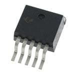
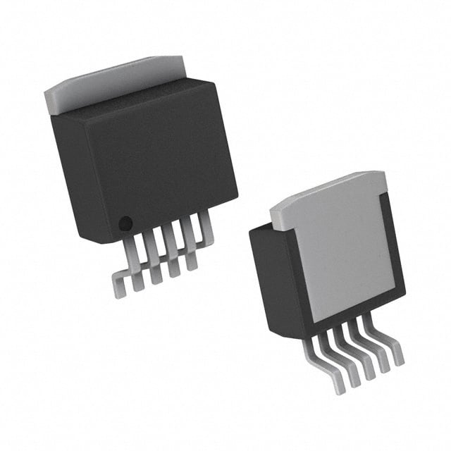
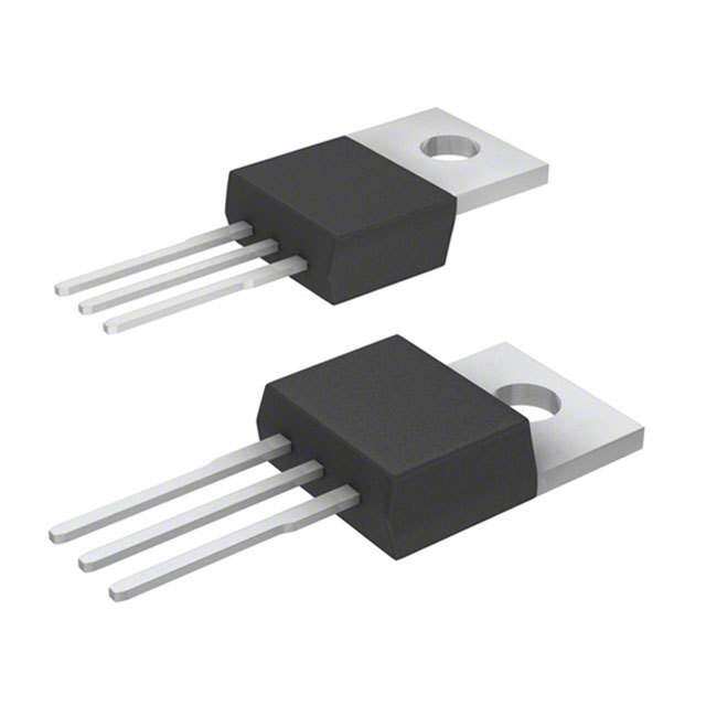
| 供应商器件封装 | DDPAK/TO-263-5 |
| 其它名称 | 296-14444-6 |
| 包装 | Digi-Reel® |
| 单位重量 | 1.456 g |
| 商标 | Texas Instruments |
| 回动电压—最大值 | 325 mV at 1 A |
| 安装类型 | 表面贴装 |
| 安装风格 | SMD/SMT |
| 封装 | Tube |
| 封装/外壳 | TO-263-6,D²Pak(5 引线+接片),TO-263BA |
| 封装/箱体 | TO-263-5 |
| 工作温度 | -40°C ~ 125°C |
| 工厂包装数量 | 50 |
| 最大工作温度 | + 150 C |
| 最大输入电压 | 5.5 V |
| 最小工作温度 | - 40 C |
| 最小输入电压 | + 2.7 V |
| 标准包装 | 1 |
| 电压-跌落(典型值) | 0.22V @ 1A |
| 电压-输入 | 最高 5.5V |
| 电压-输出 | 3.3V |
| 电压调节准确度 | 2 % |
| 电流-输出 | 1A |
| 电流-限制(最小值) | 2.4A |
| 稳压器拓扑 | 正,固定式 |
| 稳压器数 | 1 |
| 系列 | TPS79633 |
| 线路调整率 | 0.05 % / V |
| 负载调节 | 5 mV |
| 输入偏压电流—最大 | 0.265 mA |
| 输出电压 | 3.3 V |
| 输出电流 | 1 A |
| 输出端数量 | 1 Output |
| 输出类型 | Fixed |
| 配用 | /product-detail/zh/TPS78633EVM-207/296-20625-ND/562085 |


- 商务部:美国ITC正式对集成电路等产品启动337调查
- 曝三星4nm工艺存在良率问题 高通将骁龙8 Gen1或转产台积电
- 太阳诱电将投资9.5亿元在常州建新厂生产MLCC 预计2023年完工
- 英特尔发布欧洲新工厂建设计划 深化IDM 2.0 战略
- 台积电先进制程称霸业界 有大客户加持明年业绩稳了
- 达到5530亿美元!SIA预计今年全球半导体销售额将创下新高
- 英特尔拟将自动驾驶子公司Mobileye上市 估值或超500亿美元
- 三星加码芯片和SET,合并消费电子和移动部门,撤换高东真等 CEO
- 三星电子宣布重大人事变动 还合并消费电子和移动部门
- 海关总署:前11个月进口集成电路产品价值2.52万亿元 增长14.8%


PDF Datasheet 数据手册内容提取
Product Sample & Technical Tools & Support & Folder Buy Documents Software Community TPS79601,TPS79613,TPS79618,TPS79625 TPS79628,TPS79630,TPS79633,TPS79650 SLVS351P–SEPTEMBER2002–REVISEDMARCH2015 TPS796xx Ultralow-Noise, High PSRR, Fast, RF, 1-A Low-Dropout Linear Regulators 1 Features 3 Description • 1-ALow-DropoutRegulatorWithEnable The TPS796 family of low-dropout (LDO) low-power 1 linear voltage regulators features high power-supply • AvailableinFixedandAdjustable(1.2Vto5.5V) rejection ratio (PSRR), ultralow-noise, fast start-up, Versions and excellent line and load transient responses in • HighPSRR(53dBat10kHz) small outline, 3 × 3 VSON, SOT223-6, and TO-263 • Ultralow-Noise(40μV ,TPS79630) packages. Each device in the family is stable with a RMS small, 1-μF ceramic capacitor on the output. The • FastStart-UpTime(50 μs) family uses an advanced, proprietary BiCMOS • StableWitha1-μFCeramicCapacitor fabrication process to yield extremely low dropout • ExcellentLoadandLineTransientResponse voltages (for example, 250 mV at 1 A). Each device achievesfaststart-uptimes(approximately50μswith • VeryLowDropoutVoltage(250mVatFullLoad, a 0.001-μF bypass capacitor) while consuming very TPS79630) low quiescent current (265 μA typical). Moreover, • 3× 3VSON PowerPAD™,SOT223-6,and when the device is placed in standby mode, the TO-263Packages supply current is reduced to less than 1 μA. The TPS79630 exhibits approximately 40 μV of output RMS 2 Applications voltage noise at 3.0-V output, with a 0.1-μF bypass capacitor. Applications with analog components that • RF:VCOs,Receivers,ADCs are noise sensitive, such as portable RF electronics, • Audio benefit from the high PSRR, low noise features, and • Bluetooth®,WirelessLAN needfastresponsetime. • CellularandCordlessTelephones DeviceInformation(1) • HandheldOrganizers,PDAs PARTNUMBER PACKAGE BODYSIZE(NOM) VSON(8) 3.00mm×3.00mm TPS796 SOT-223(6) 6.50mm×3.50mm TO-263(5) 10.16mm×8.42mm (1) For all available packages, see the orderable addendum at theendofthedatasheet. RippleRejectionvsFrequency TPS79630 OutputSpectralNoiseDensityvsFrequency TPS79630 80 ection (dB) 76540000 IOUT= I1O UmTA= 1A CCNORU=TV =0IN .10=01 4mm VFF Density (V/)HzmÖ 0000....7654 VCCIONNRU=T= =5 0. 52.1 .V2mmFF Ripple Rej 3200 ectral Noise 00..32 IOUT= 1A p 10 S ut 0.1 0 utp IOUT= 1.5A O 1 10 100 1 k 10 k 100 k 1 M 10M 0 100 1 k 10 k 100 k Frequency (Hz) Frequency (Hz) 1 An IMPORTANT NOTICE at the end of this data sheet addresses availability, warranty, changes, use in safety-critical applications, intellectualpropertymattersandotherimportantdisclaimers.PRODUCTIONDATA.
TPS79601,TPS79613,TPS79618,TPS79625 TPS79628,TPS79630,TPS79633,TPS79650 SLVS351P–SEPTEMBER2002–REVISEDMARCH2015 www.ti.com Table of Contents 1 Features.................................................................. 1 8.1 ApplicationInformation............................................14 2 Applications........................................................... 1 8.2 TypicalApplication..................................................14 3 Description............................................................. 1 8.3 Do'sandDon'ts ......................................................17 4 RevisionHistory..................................................... 2 9 PowerSupplyRecommendations...................... 17 5 PinConfigurationandFunctions......................... 3 10 Layout................................................................... 17 10.1 LayoutGuidelines.................................................17 6 Specifications......................................................... 4 10.2 LayoutExamples...................................................18 6.1 AbsoluteMaximumRatings......................................4 10.3 ThermalConsiderations........................................19 6.2 ESDRatings ............................................................4 10.4 EstimatingJunctionTemperature ........................20 6.3 RecommendedOperatingConditions.......................4 11 DeviceandDocumentationSupport................. 22 6.4 ThermalInformation..................................................5 6.5 ElectricalCharacteristics...........................................6 11.1 DeviceSupport......................................................22 6.6 TypicalCharacteristics..............................................7 11.2 DocumentationSupport........................................22 11.3 RelatedLinks........................................................22 7 DetailedDescription............................................ 11 11.4 Trademarks...........................................................23 7.1 Overview.................................................................11 11.5 ElectrostaticDischargeCaution............................23 7.2 FunctionalBlockDiagrams.....................................11 11.6 Glossary................................................................23 7.3 FeatureDescription.................................................12 12 Mechanical,Packaging,andOrderable 7.4 DeviceFunctionalModes........................................13 Information........................................................... 23 8 ApplicationandImplementation........................ 14 4 Revision History NOTE:Pagenumbersforpreviousrevisionsmaydifferfrompagenumbersinthecurrentversion. ChangesfromRevisionO(November2013)toRevisionP Page • AddedESDRatingstable,FeatureDescriptionsection,DeviceFunctionalModes,ApplicationandImplementation section,PowerSupplyRecommendationssection,Layoutsection,DeviceandDocumentationSupportsection,and Mechanical,Packaging,andOrderableInformationsection ................................................................................................. 1 • Changedfront-pagefigure;updatedgraphstyle,replaceddevicepinoutswithapplicationcircuits ..................................... 1 • ChangedPinConfigurationandFunctionssection;updatedtableformatandaddedpinoutdrawings................................. 3 • Changed"free-air"to"junction"temperatureinconditionstatementforAbsoluteMaximumRatings .................................. 4 • ChangedV accuracyforTPS79601,testconditionsandspecifiedvalues ...................................................................... 6 OUT • DeletedStart-uptimesymbol................................................................................................................................................. 6 • AddedThermalshutdowntemperaturespecificationtoElectricalCharacteristics ................................................................ 6 • AddedOperatingjunctiontemperaturespecificationtoElectricalCharacteristics ................................................................ 6 • AddedconditionstatementtoTypicalCharacteristics........................................................................................................... 7 ChangesfromRevisionN(January2011)toRevisionO Page • ChangedPower-SupplyRippleRejection3rdtestconditionfrom"f=10Hz"to"f=10kHz"(typo).................................... 6 • ChangedPower-SupplyRippleRejection4thtestconditionfrom"f=100Hz"to"f=100kHz"(typo) ................................ 6 ChangesfromRevisionM(October2010)toRevisionN Page • Correctedtypoinfront-pagefigure......................................................................................................................................... 1 ChangesfromRevisionL(August2010)toRevisionM Page • CorrectedtypoinFigure32 ................................................................................................................................................. 21 2 SubmitDocumentationFeedback Copyright©2002–2015,TexasInstrumentsIncorporated ProductFolderLinks:TPS79601 TPS79613 TPS79618 TPS79625TPS79628 TPS79630 TPS79633 TPS79650
TPS79601,TPS79613,TPS79618,TPS79625 TPS79628,TPS79630,TPS79633,TPS79650 www.ti.com SLVS351P–SEPTEMBER2002–REVISEDMARCH2015 5 Pin Configuration and Functions DCQPackage 6-PinSOT-223 KTTPackage TopView 5-PinTO-263 TopView EN 1 6 IN 2 GND 3 OUT 4 1 2 3 4 5 NR/FB 5 EN GND NR/FB IN OUT DRBPackage 8-PinVSON TopView IN 1 8 EN IN 2 7 N/C OUT 3 6 GND OUT 4 5 NR/FB PinFunctions PIN SOT223 I/O DESCRIPTION NAME VSON TO-263 Drivingtheenablepin(EN)highturnsontheregulator.Drivingthispinlowputsthe EN 1 8 I regulatorintoshutdownmode.ENcanbeconnectedtoINifnotused. FB 5 5 I Thisterminalisthefeedbackinputvoltagefortheadjustabledevice. 6, Regulatorground GND 3,Tab — PowerPAD IN 2 1,2 I Unregulatedinputtothedevice. N/C — 7 — Notinternallyconnected.Thispinmusteitherbeleftopen,ortiedtoGND. Connectinganexternalcapacitortothispinbypassesnoisegeneratedbythe NR 5 5 — internalbandgap.Thisimprovespower-supplyrejectionandreducesoutputnoise. OUT 4 3,4 O Outputoftheregulator. Copyright©2002–2015,TexasInstrumentsIncorporated SubmitDocumentationFeedback 3 ProductFolderLinks:TPS79601 TPS79613 TPS79618 TPS79625TPS79628 TPS79630 TPS79633 TPS79650
TPS79601,TPS79613,TPS79618,TPS79625 TPS79628,TPS79630,TPS79633,TPS79650 SLVS351P–SEPTEMBER2002–REVISEDMARCH2015 www.ti.com 6 Specifications 6.1 Absolute Maximum Ratings overoperatingjunctiontemperaturerange(unlessotherwisenoted) (1) MIN MAX UNIT IN –0.3 6 Voltage EN –0.3 V +0.3 V IN OUT 6 Current Peakoutput Internallylimited Powerdissipation Continuoustotal SeeThermalInformation Junction,T –40 150 J Temperature °C Storage,T –65 150 stg (1) StressesbeyondthoselistedunderAbsoluteMaximumRatingsmaycausepermanentdamagetothedevice.Thesearestressratings only,whichdonotimplyfunctionaloperationofthedeviceattheseoranyotherconditionsbeyondthoseindicatedunderRecommended OperatingConditions.Exposuretoabsolute-maximum-ratedconditionsforextendedperiodsmayaffectdevicereliability. 6.2 ESD Ratings VALUE UNIT Humanbodymodel(HBM),perANSI/ESDA/JEDECJS-001,allpins(1) ±2000 V(ESD) Electrostaticdischarge Chargeddevicemodel(CDM),perJEDECspecificationJESD22-C101, V allpins(2) ±500 (1) JEDECdocumentJEP155statesthat500-VHBMallowssafemanufacturingwithastandardESDcontrolprocess. (2) JEDECdocumentJEP157statesthat250-VCDMallowssafemanufacturingwithastandardESDcontrolprocess. 6.3 Recommended Operating Conditions overoperatingjunctiontemperaturerange(unlessotherwisenoted) MIN NOM MAX UNIT V Inputvoltage 2.7 5.5 V IN I Outputcurrent 0 1 A OUT T Operatingjunctiontemperature –40 125 °C J 4 SubmitDocumentationFeedback Copyright©2002–2015,TexasInstrumentsIncorporated ProductFolderLinks:TPS79601 TPS79613 TPS79618 TPS79625TPS79628 TPS79630 TPS79633 TPS79650
TPS79601,TPS79613,TPS79618,TPS79625 TPS79628,TPS79630,TPS79633,TPS79650 www.ti.com SLVS351P–SEPTEMBER2002–REVISEDMARCH2015 6.4 Thermal Information TPS796xx(3) THERMALMETRIC(1) (2) DRB(VSON) DCQ KTT(TO-263) UNIT (SOT-223) 8PINS 6PINS 5PINS R Junction-to-ambientthermalresistance 47.8 70.4 25 θJA R Junction-to-case(top)thermalresistance 83 70 35 θJC(top) R Junction-to-boardthermalresistance N/A N/A N/A θJB °C/W ψ Junction-to-topcharacterizationparameter 2.1 6.8 1.5 JT ψ Junction-to-boardcharacterizationparameter 17.8 30.1 8.52 JB R Junction-to-case(bottom)thermalresistance 12.1 6.3 0.4 θJC(bot) (1) Formoreinformationabouttraditionalandnewthermalmetrics,seetheICPackageThermalMetricsapplicationreport,SPRA953. (2) ForthermalestimatesofthisdevicebasedonPCBcopperarea,seetheTIPCBThermalCalculator. (3) ThermaldatafortheDRB,DCQ,andDRVpackagesarederivedbythermalsimulationsbasedonJEDEC-standardmethodologyas specifiedintheJESD51series.Thefollowingassumptionsareusedinthesimulations: (a) i. DRB: The exposed pad is connected to the PCB ground layer through a 2 × 2 thermal via array. . ii. DCQ: The exposed pad is connected to the PCB ground layer through a 3 × 2 thermal via array. .iii.KTT:TheexposedpadisconnectedtothePCBgroundlayerthrougha5×4thermalviaarray. (b) i.DRB:Thetopandbottomcopperlayersareassumedtohavea20%thermalconductivityofcopperrepresentinga20%copper coverage. . ii. DCQ: Each of top and bottom copper layers has a dedicated pattern for 20% copper coverage. .iii.KTT:Thetopandbottomcopperlayersareassumedtohavea20%thermalconductivityofcopperrepresentinga20%copper coverage. (c)ThesedataweregeneratedwithonlyasingledeviceatthecenterofaJEDEChigh-K(2s2p)boardwith3in×3incopperarea.To understandtheeffectsofthecopperareaonthermalperformance,seePowerDissipationandEstimatingJunctionTemperature. Copyright©2002–2015,TexasInstrumentsIncorporated SubmitDocumentationFeedback 5 ProductFolderLinks:TPS79601 TPS79613 TPS79618 TPS79625TPS79628 TPS79630 TPS79633 TPS79650
TPS79601,TPS79613,TPS79618,TPS79625 TPS79628,TPS79630,TPS79633,TPS79650 SLVS351P–SEPTEMBER2002–REVISEDMARCH2015 www.ti.com 6.5 Electrical Characteristics Overrecommendedoperatingtemperaturerange(T =–40°Cto125°C),V =V ,V =V +1V(1),I =1mA,C J EN IN, IN OUT(nom) OUT OUT =10μF,andC =0.01μF,unlessotherwisenoted.Typicalvaluesareat25°C. NR PARAMETER TESTCONDITIONS MIN TYP MAX UNIT VIN Inputvoltage(1) 2.7 5.5 V VFB Internalreference(TPS79601) 1.2 1.225 1.25 V IOUT Continuousoutputcurrent 0 1 A Outputvoltage range TPS79601 1.225 5.5–VDO V VOUT TPS79601(2) 0μA≤IOUT≤1A,VOUT(nom)+1V≤VIN≤5.5V(1) 0.98VOUT(nom) VOUT(nom) 1.02VOUT(nom) V Accuracy FixedVOUT<5V 0μA≤IOUT≤1A,VOUT(nom)+1V≤VIN≤5.5V(1) –2% 2% FixedVOUT=5V 0μA≤IOUT≤1A,VOUT(nom)+1V≤VIN≤5.5V(1) –3% 3% ΔVO(ΔVI) Lineregulation(1) VOUT+1V≤VIN≤5.5V 0.05 0.12 %/V ΔVO(ΔIO) Loadregulation 0μA≤IOUT≤1A 5 mV TPS79628 IOUT=1A 270 365 Dropoutvoltage(3) TPS79628DRB IOUT=250mA 52 90 VDO (VIN=VOUT(nom)– TPS79630 IOUT=1A 250 345 mV 0.1V) TPS79633 IOUT=1A 220 325 TPS79650 IOUT=1A 200 300 ICL Outputcurrentlimit VOUT=0V 2.4 4.2 A IGND Groundpincurrent 0μA≤IOUT≤1A 265 385 μA ISHDN Shutdowncurrent(4) VEN=0V,2.7V≤VIN≤5.5V 0.07 1 μA IFB Feedbackpincurrent VFB=1.225V 1 µA f=100Hz.IOUT=10mA 59 Power-supplyrejectionratio f=100Hz,IOUT=1A 54 PSRR dB (TPS79630) f=10kHz,IOUT=1A 53 f=100kHz,IOUT=1A 42 CNR=0.001μF 54 BW=100Hzto100kHz, CNR=0.0047μF 46 Vn Outputnoisevoltage(TPS79630) IOUT=1A CNR=0.01μF 41 μVRMS CNR=0.1μF 40 CNR=0.001μF 50 Start-uptime(TPS79630) RCLOU=T3=Ω1,μF CNR=0.0047μF 75 μs CNR=0.01μF 110 VEN(HI) Enablehigh(enabled) 2.7V≤VIN≤5.5V 1.7 VIN V VEN(LO) Enablelow(shutdown) 2.7V≤VIN≤5.5V 0 0.7 V IEN(HI) Enablepincurrent,enabled VEN=0V –1 1 μA Undervoltagelockout VCCrising 2.25 2.65 V UVLO Hysteresis 100 mV Shutdown,temperatureincreasing 165 Tsd Thermalshutdowntemperature °C Reset,temperaturedecreasing 140 TJ Operatingjunctiontemperature –40 125 °C (1) MinimumV =V +V or2.7V,whicheverisgreater.TPS79650istestedatV =5.5V. IN OUT DO IN (2) Toleranceofexternalresistorsnotincludedinthisspecification. (3) V isnotmeasuredforTPS79618andTPS79625becauseminimumV =2.7V. DO IN (4) Foradjustableversion,thisappliesonlyafterV isapplied;thenV transitionshightolow. IN EN 6 SubmitDocumentationFeedback Copyright©2002–2015,TexasInstrumentsIncorporated ProductFolderLinks:TPS79601 TPS79613 TPS79618 TPS79625TPS79628 TPS79630 TPS79633 TPS79650
TPS79601,TPS79613,TPS79618,TPS79625 TPS79628,TPS79630,TPS79633,TPS79650 www.ti.com SLVS351P–SEPTEMBER2002–REVISEDMARCH2015 6.6 Typical Characteristics AtV =V ,V =V +1V,I =1mA,C =10µF,C =0.01µF,C =2.2µF,andT =25°C,unlessotherwise EN IN IN OUT(nom) OUT OUT NR IN J noted. 3.05 2.7945 3.04 VIN=4V VIN=3.8V COUT=10mF COUT=10mF 3.03 TJ=25°C 2.7930 IOUT=1mA 3.02 3.01 V) 3.00 V) 2.7825 (UT 2.99 (UT IOUT=1A O O V 2.98 V 2.7810 2.97 2.96 2.95 2.7705 0.0 0.2 0.4 0.6 0.8 1.0 −40−25−10 5 20 35 50 65 80 95110125 IOUT(A) TJ(°C) Figure1.TPS79630OutputVoltagevsOutputCurrent Figure2.TPS79628OutputVoltagevs JunctionTemperature 350 0.7 340 VCIONU=T3=.810VmF V/HzmÖ 0.6 VCCIONNRU=T=5=0.5.21.V2mmFF 330 sity− 0.5 n (A)mND 320 IOUT=1A Noise De 00..34 IG 310 ctral 0.2 IOUT=1mA IOUT=1mA pe S 300 ut 0.1 utp IOUT=1.5A 290 O 0.0 −40−25−10 5 20 35 50 65 80 95110125 100 1k 10k 100k TJ(°C) Frequency (Hz) Figure3.TPS79628GroundCurrentvs Figure4.TPS79630OutputSpectralNoiseDensityvs JunctionTemperature Frequency 0.6 2.5 Hz VIN=5.5V Hz VIN=5.5V V/−mÖ 0.5 CCONRUT==0.110mmFF V/−mÖ 2.0 CNR=0.01mF CIOOUUTT==11A0mF y y sit 0.4 sit Den Den 1.5 CNR=0.1mF se 0.3 IOUT=1mA se ectral Noi 0.2 ectral Noi 1.0 CNRC=N0R.0=0407.0m0F1mF ut Sp 0.1 IOUT=1A ut Sp 0.5 p p ut ut O O 0.0 0.0 100 1k 10k 100k 100 1k 10k 100k Frequency (Hz) Frequency (Hz) Figure5.TPS79630OutputSpectralNoiseDensityvs Figure6.TPS79630OutputSpectralNoiseDensityvs Frequency Frequency Copyright©2002–2015,TexasInstrumentsIncorporated SubmitDocumentationFeedback 7 ProductFolderLinks:TPS79601 TPS79613 TPS79618 TPS79625TPS79628 TPS79630 TPS79633 TPS79650
TPS79601,TPS79613,TPS79618,TPS79625 TPS79628,TPS79630,TPS79633,TPS79650 SLVS351P–SEPTEMBER2002–REVISEDMARCH2015 www.ti.com Typical Characteristics (continued) AtV =V ,V =V +1V,I =1mA,C =10µF,C =0.01µF,C =2.2µF,andT =25°C,unlessotherwise EN IN IN OUT(nom) OUT OUT NR IN J noted. 60 350 S Voise−mRM 50 235000 VCIONU=T=2.170VmF IOUT=1A N 40 ut ared Outp 30 V(mV)DO 125000 Squ 20 100 n Root Mea 100 ICBOWOUUT=T==12015000HmmzFAto100kHz 500 IOUT=250mA S− 0.001mF 0.0047mF 0.01mF 0.1mF -40-25-10 5 20 35 50 65 80 95110125 M R CNR(mF) TJ(°C) Figure7.TPS79630RootMeanSquaredOutputNoisevs Figure8.TPS79628DropoutVoltagevs BypassCapacitance JunctionTemperature 80 80 VIN=4V VIN=4V 70 COUT=10mF 70 COUT=10mF IOUT=1mA CNR=0.01mF IOUT=1mA CNR=0.1mF 60 B 60 d Ripple Rejection−dB 23450000 IOUT=1A Ripple Rejection− 23450000 IOUT=1A 10 10 0 0 1 10 100 1k 10k 100k 1M 10M 1 10 100 1k 10k 100k 1M 10M Frequency (Hz) Frequency (Hz) Figure9.TPS79630RippleRejectionvsFrequency Figure10.TPS79630RippleRejectionvsFrequency 80 3 VIN=4V 2.75 VIN=4V, 70 IOUT=1mA CCONRUT==0.20.12mmFF 2.50 CIOOUUTT==11.00AmF, C0.N0R04=7mF e Rejection−dB 34560000 IOUT=1A V(V)OUT 1112....257250552 C0.N0R01=mF C0.N0R1E=mnFable pl 1 p Ri 20 0.75 10 0.50 0.25 0 0 1 10 100 1k 10k 100k 1M 10M 0 100 200 300 400 500 600 Frequency (Hz) t (µs) Figure11.TPS79630RippleRejectionvsFrequency Figure12. Start-UpTime 8 SubmitDocumentationFeedback Copyright©2002–2015,TexasInstrumentsIncorporated ProductFolderLinks:TPS79601 TPS79613 TPS79618 TPS79625TPS79628 TPS79630 TPS79633 TPS79650
TPS79601,TPS79613,TPS79618,TPS79625 TPS79628,TPS79630,TPS79633,TPS79650 www.ti.com SLVS351P–SEPTEMBER2002–REVISEDMARCH2015 Typical Characteristics (continued) AtV =V ,V =V +1V,I =1mA,C =10µF,C =0.01µF,C =2.2µF,andT =25°C,unlessotherwise EN IN IN OUT(nom) OUT OUT NR IN J noted. 5 6 4 5 V) V) ( ( N 3 N 4 VI VI 402 ICCOONURUTT===011.0A01mmFF ddvt 1µVs 403 ICCONOURUTT===011.0A01mmFF ddvt 1µVs V) 20 V) 20 m m (OUT 0 (OUT 0 V V D−20 D −20 −40 −40 0 20 40 60 80 100120140160180200 0 20 40 60 80 100120140160180200 t (ms) t (ms) Figure13.TPS79618LineTransientResponse Figure14.TPS79630LineTransientResponse 2 4.0 VOUT=2.5V A) 1 3.5 RL=10W (UT 0 3.0 CNR=0.01mF O I −1 VIN=3.8V di 1A v 2.5 COUT=10mF dt µs Di 150 CNR=0.01mF mV/ 2.0 0 V) 75 50 1.5 (mT 0 1.0 VIN U O VD −75 0.5 VOUT −150 0 0 100 2003004005006007008009001000 0 1 2 3 4 5 6 7 8 9 10 t (ms) 200ms/Div Figure15.TPS79628LoadTransientResponse Figure16.TPS79625PowerUp/PowerDown 350 300 300 250 250 TJ=125°C TJ=125°C 200 mV) 200 TJ=25°C mV) TJ=25°C (DO 150 (DO 150 V V TJ=−40°C 100 100 TJ=−40°C 50 50 ICOOUUTT==11A0µF CNR=0.01µF 0 0 0 1002003004005006007008009001000 2.5 3.0 3.5 4.0 4.5 5.0 IOUT(mA) VIN(V) Figure17.TPS79630DropoutVoltagevsOutputCurrent Figure18.TPS79601DropoutVoltagevsInputVoltage Copyright©2002–2015,TexasInstrumentsIncorporated SubmitDocumentationFeedback 9 ProductFolderLinks:TPS79601 TPS79613 TPS79618 TPS79625TPS79628 TPS79630 TPS79633 TPS79650
TPS79601,TPS79613,TPS79618,TPS79625 TPS79628,TPS79630,TPS79633,TPS79650 SLVS351P–SEPTEMBER2002–REVISEDMARCH2015 www.ti.com Typical Characteristics (continued) AtV =V ,V =V +1V,I =1mA,C =10µF,C =0.01µF,C =2.2µF,andT =25°C,unlessotherwise EN IN IN OUT(nom) OUT OUT NR IN J noted. 100 100 W− COUT=1µF −W COUT=2.2mF Resistance 10 RInesgtaiobnilitoyf Resistance 10 RInesgtaiobnilitoyf Series 1 Series 1 Equivalent 0.1 RegionofStability Equivalent 0.1 RegionofStability − − R R S S E E 0.01 0.01 1 10 30 60 125 250 500 750 1000 1 10 30 60 125 250 500 750 1000 IOUT(mA) IOUT(mA) Figure19.TPS79630TypicalRegionsofStabilityEquivalent Figure20.TPS79630TypicalRegionsofStabilityEquivalent SeriesResistance(ESR)vsOutputCurrent SeriesResistance(ESR)vsOutputCurrent 100 W − COUT=10.0mF e c n sta 10 Regionof si Instability e R s e Seri 1 nt e RegionofStability al v ui q 0.1 E − R S E 0.01 1 10 30 60 125 250 500 750 1000 IOUT(mA) Figure21.TPS79630TypicalRegionsofStabilityEquivalentSeriesResistance(ESR)vsOutputCurrent 10 SubmitDocumentationFeedback Copyright©2002–2015,TexasInstrumentsIncorporated ProductFolderLinks:TPS79601 TPS79613 TPS79618 TPS79625TPS79628 TPS79630 TPS79633 TPS79650
TPS79601,TPS79613,TPS79618,TPS79625 TPS79628,TPS79630,TPS79633,TPS79650 www.ti.com SLVS351P–SEPTEMBER2002–REVISEDMARCH2015 7 Detailed Description 7.1 Overview The TPS796 family of low-dropout (LDO) regulators combines the high performance required of many RF and precision analog applications with low current consumption. High PSRR is provided by a high-gain, high- bandwidth error loop with good supply rejection at very low headroom (V – V ). A noise-reduction pin is IN OUT provided to bypass noise generated by the band-gap reference and to improve PSRR, while a quick-start circuit quickly charges this capacitor at start-up. All versions have thermal and overcurrent protection, and are fully specifiedfrom–40°Cto125°C. 7.2 Functional Block Diagrams IN OUT UVLO Current Sense ILIM SHUTDOWN GND R 1 FB EN UVLO R 2 Thermal Shutdown Quickstart External to the device Bandgap V V Reference REF IN 1.225 V 250 kW Figure22. FunctionalBlockDiagram—AdjustableVersion IN OUT UVLO Current Sense ILIM SHUTDOWN GND R 1 EN UVLO R 2 Thermal Shutdown Quickstart R2= 40 kW Bandgap V VIN R1e.f2e2re5n Vce REF NR 250 kW Figure23. FunctionalBlockDiagram—FixedVersion Copyright©2002–2015,TexasInstrumentsIncorporated SubmitDocumentationFeedback 11 ProductFolderLinks:TPS79601 TPS79613 TPS79618 TPS79625TPS79628 TPS79630 TPS79633 TPS79650
TPS79601,TPS79613,TPS79618,TPS79625 TPS79628,TPS79630,TPS79633,TPS79650 SLVS351P–SEPTEMBER2002–REVISEDMARCH2015 www.ti.com 7.3 Feature Description 7.3.1 Shutdown The enable pin (EN) is active high and is compatible with standard and low-voltage TTL-CMOS levels. When shutdowncapabilityisnotrequired,ENcanbeconnectedtoIN. 7.3.2 Start-Up The TPS796 uses a start-up circuit to quickly charge the noise reduction capacitor, C , if present (see the NR Functional Block Diagrams). This circuit allows for the combination of very low output noise and fast start-up times. The NR pin is high impedance so a low leakage C capacitor must be used; most ceramic capacitors are NR appropriateforthisconfiguration. For the fastest start-up, apply V first, and then drive the enable pin (EN) high. If EN is tied to IN, start-up is IN somewhatslower.ToensurethatC isfullychargedduringstart-up,usea0.1-μForsmallercapacitor. NR 7.3.3 UndervoltageLockout(UVLO) The TPS796 uses an undervoltage lockout circuit to keep the output shut off until internal circuitry is operating properly. The UVLO circuit has approximately 100 mV of hysteresis to help reject input voltage drops when the regulatorfirstturnson. 7.3.4 RegulatorProtection The TPS796xx PMOS-pass transistor has a built-in back diode that conducts reverse current when the input voltage drops below the output voltage (for example, during power-down). Current is conducted from the output to the input and is not internally limited. If extended reverse voltage operation is anticipated, external limiting mightbeappropriate. The TPS796xx features internal current limiting and thermal protection. During normal operation, the TPS796xx limits output current to approximately 2.8 A. When current limiting engages, the output voltage scales back linearly until the overcurrent condition ends. While current limiting is designed to prevent gross device failure, care should be taken not to exceed the power dissipation ratings of the package. If the temperature of the device exceeds approximately 165°C (T ), thermal-protection circuitry shuts it down. Once the device has cooled down sd tobelowapproximately140°C,regulatoroperationresumes. 12 SubmitDocumentationFeedback Copyright©2002–2015,TexasInstrumentsIncorporated ProductFolderLinks:TPS79601 TPS79613 TPS79618 TPS79625TPS79628 TPS79630 TPS79633 TPS79650
TPS79601,TPS79613,TPS79618,TPS79625 TPS79628,TPS79630,TPS79633,TPS79650 www.ti.com SLVS351P–SEPTEMBER2002–REVISEDMARCH2015 7.4 Device Functional Modes Table1providesaquickcomparisonbetweenthenormal,dropout,anddisabledmodesofoperation. Table1.DeviceFunctionalModeComparison PARAMETER OPERATINGMODE V EN I T IN OUT J Normal V >V +V V >V I <I T <T IN OUT(nom) DO EN EN(HI) OUT CL J SD Dropout V <V +V V >V I <I T <T IN OUT(nom) DO EN EN(HI) OUT CL J SD Disabled — V <V — T >T EN EN(LO) J SD 7.4.1 NormalOperation Thedeviceregulatestothenominaloutputvoltageunderthefollowingconditions: • Theinputvoltageisgreaterthanthenominaloutputvoltageplusthedropoutvoltage(V +V ). OUT(nom) DO • The enable voltage has previously exceeded the enable rising threshold voltage and not yet decreased below theenablefallingthreshold. • Theoutputcurrentislessthanthecurrentlimit(I <I ). OUT CL • Thedevicejunctiontemperatureislessthanthethermalshutdowntemperature(T <T ). J SD 7.4.2 DropoutOperation If the input voltage is lower than the nominal output voltage plus the specified dropout voltage, but all other conditions are met for normal operation, the device operates in dropout mode. In this mode, the output voltage tracks the input voltage. During this mode, the transient performance of the device becomes significantly degraded because the pass device is in a triode state and no longer controls the current through the LDO. Line orloadtransientsindropoutcanresultinlargeoutput-voltagedeviations. 7.4.3 Disabled Thedeviceisdisabledunderthefollowingconditions: • The enable voltage is less than the enable falling threshold voltage or has not yet exceeded the enable rising threshold. • Thedevicejunctiontemperatureisgreaterthanthethermalshutdowntemperature(T >T ). J SD Copyright©2002–2015,TexasInstrumentsIncorporated SubmitDocumentationFeedback 13 ProductFolderLinks:TPS79601 TPS79613 TPS79618 TPS79625TPS79628 TPS79630 TPS79633 TPS79650
TPS79601,TPS79613,TPS79618,TPS79625 TPS79628,TPS79630,TPS79633,TPS79650 SLVS351P–SEPTEMBER2002–REVISEDMARCH2015 www.ti.com 8 Application and Implementation NOTE Information in the following applications sections is not part of the TI component specification, and TI does not warrant its accuracy or completeness. TI’s customers are responsible for determining suitability of components for their purposes. Customers should validateandtesttheirdesignimplementationtoconfirmsystemfunctionality. 8.1 Application Information The TPS796xx family of low-dropout (LDO) regulators has been optimized for use in noise-sensitive equipment. The device features extremely low dropout voltages, high PSRR, ultralow output noise, low quiescent current (265μAtypically),andenableinputtoreducesupplycurrentstolessthan1 μAwhentheregulatoristurnedoff. 8.2 Typical Application AtypicalapplicationcircuitisshowninFigure24. VIN IN OUT VOUT TPS796xx 2.2m F 1 m F EN GND NR 0.01m F Figure24. TypicalApplicationCircuit 8.2.1 DesignRequirements Table2liststhedesignparameters. Table2.DesignParameters PARAMETER DESIGNREQUIREMENT Inputvoltage 3.3V Outputvoltage 2.5V Maximumoutputcurrent 700mA 8.2.2 DetailedDesignProcedure Selectthedesireddevicebasedontheoutputvoltage. Provide an input supply with adequate headroom to account for dropout and output current to account for the GNDterminalcurrent,andpowertheload. 8.2.2.1 InputandOutputCapacitorRequirements A 2.2-μF or larger ceramic input bypass capacitor, connected between IN and GND and located close to the TPS796xx, is required for stability and improves transient response, noise rejection, and ripple rejection. A higher-value input capacitor may be necessary if large, fast-rise-time load transients are anticipated and the deviceislocatedseveralinchesfromthepowersource. Like most low dropout regulators, the TPS796xx requires an output capacitor connected between OUT and GND to stabilize the internal control loop. The minimum recommended capacitor is 1 μF. Any 1-μF or larger ceramic capacitorissuitable. 14 SubmitDocumentationFeedback Copyright©2002–2015,TexasInstrumentsIncorporated ProductFolderLinks:TPS79601 TPS79613 TPS79618 TPS79625TPS79628 TPS79630 TPS79633 TPS79650
TPS79601,TPS79613,TPS79618,TPS79625 TPS79628,TPS79630,TPS79633,TPS79650 www.ti.com SLVS351P–SEPTEMBER2002–REVISEDMARCH2015 8.2.2.2 OutputNoise The internal voltage reference is a key source of noise in an LDO regulator. The TPS796xx has an NR pin which is connected to the voltage reference through a 250-kΩ internal resistor. The 250-kΩ internal resistor, in conjunction with an external bypass capacitor connected to the NR pin, creates a low-pass filter to reduce the voltage reference noise and, therefore, the noise at the regulator output. In order for the regulator to operate properly, the current flow out of the NR pin must be at a minimum, because any leakage current creates an IR drop across the internal resistor, thus creating an output error. Therefore, the bypass capacitor must have minimal leakage current. The bypass capacitor should be no more than 0.1 μF in order to ensure that it is fully chargedduringthequickstarttimeprovidedbytheinternalswitchshowninthefunctionalblockdiagram. For example, the TPS79630 exhibits 40 μV of output voltage noise using a 0.1-μF ceramic bypass capacitor RMS and a 10-μF ceramic output capacitor. The output starts up slower as the bypass capacitance increases due to theRCtimeconstantatthebypasspinthatiscreatedbytheinternal250-kΩresistorandexternalcapacitor. 8.2.2.3 DropoutVoltage The TPS796 uses a PMOS pass transistor to achieve a low dropout voltage. When (V – V ) is less than the IN OUT dropout voltage (V ), the PMOS pass device is in its linear region of operation and r of the PMOS pass DO DS(on) element is the input-to-output resistance. Because the PMOS device behaves like a resistor in dropout, V DO approximatelyscaleswiththeoutputcurrent. As with any linear regulator, PSRR degrades as (V – V ) approaches dropout. This effect is illustrated in IN OUT Figure9 throughFigure11inTypicalCharacteristics. Copyright©2002–2015,TexasInstrumentsIncorporated SubmitDocumentationFeedback 15 ProductFolderLinks:TPS79601 TPS79613 TPS79618 TPS79625TPS79628 TPS79630 TPS79633 TPS79650
TPS79601,TPS79613,TPS79618,TPS79625 TPS79628,TPS79630,TPS79633,TPS79650 SLVS351P–SEPTEMBER2002–REVISEDMARCH2015 www.ti.com 8.2.2.4 ProgrammingtheTPS79601AdjustableLDORegulator The output voltage of the TPS79601 adjustable regulator is programmed using an external resistor divider, as Figure25shows. OUTPUT VOLTAGE VIN IN OUT VOUT PROGRAMMING GUIDE 2.2mF EN TPS79601 R1 C1 OUTPUT 1mF VOLTAGE R1 R2 C1 GND FB R2 1.8 V 14.0 kW 30.1 kW 33 pF 3.6 V 57.9 kW 30.1 kW 15 pF Figure25. TypicalApplication,AdjustableOutput TheoutputvoltageiscalculatedusingEquation1: § R1· V V u¨1(cid:14) ¸ OUT REF © R2¹ where • V =1.2246Vtypical(theinternalreferencevoltage) (1) REF Resistors R and R should be chosen for approximately 40-μA divider current. Lower value resistors can be 1 2 used for improved noise performance, but the device wastes more power. Higher values should be avoided, as leakagecurrentatFBincreasestheoutputvoltageerror. TherecommendeddesignprocedureistochooseR =30.1kΩtosetthedividercurrentat40 μA,C =15pFfor 2 1 stability,andthencalculateR usingEquation2: 1 §V · R1 ¨ OUT (cid:16)1¸uR2 ©V ¹ REF (2) In order to improve the stability of the adjustable version, it is suggested that a small compensation capacitor be placedbetweenOUTandFB.TheapproximatevalueofthiscapacitorcanbecalculatedasEquation3: (cid:11)3u10(cid:16)7(cid:12)u(cid:11)R1(cid:14)R2(cid:12) C1 (cid:11)R1uR2(cid:12) (3) The suggested value of this capacitor for several resistor ratios is shown in the table in Figure 25. If this capacitor is not used (such as in a unity-gain configuration) then the minimum recommended output capacitor is 2.2 μFinsteadof1 μF. 8.2.3 ApplicationCurves 0.6 80 Hz VIN=5.5V VIN=4V V/Ö 0.5 COUT=10mF 70 COUT=10mF m CNR=0.1mF IOUT=1mA CNR=0.1mF − B 60 y d ut Spectral Noise Densit 0000....1234 IOUTI=OU1TA=1mA Ripple Rejection− 23450000 IOUT=1A p 10 ut O 0.0 0 100 1k 10k 100k 1 10 100 1k 10k 100k 1M 10M Frequency (Hz) Frequency (Hz) Figure26.TPS79630OutputSpectralNoiseDensityvs Figure27.TPS79630RippleRejectionvsFrequency Frequency 16 SubmitDocumentationFeedback Copyright©2002–2015,TexasInstrumentsIncorporated ProductFolderLinks:TPS79601 TPS79613 TPS79618 TPS79625TPS79628 TPS79630 TPS79633 TPS79650
TPS79601,TPS79613,TPS79618,TPS79625 TPS79628,TPS79630,TPS79633,TPS79650 www.ti.com SLVS351P–SEPTEMBER2002–REVISEDMARCH2015 8.3 Do's and Don'ts Placeatleastone1-µFceramiccapacitorascloseaspossibletotheOUTpinoftheregulator. Donotplacetheoutputcapacitormorethan10mmawayfromtheregulator. Connect a 2.2-μF low equivalent series resistance (ESR) capacitor across the IN pin and GND input of the regulator. Donotexceedtheabsolutemaximumratings. 9 Power Supply Recommendations These devices are designed to operate from an input voltage supply range between 2.7 V and 5.5 V. The input voltage range provides adequate headroom in order for the device to have a regulated output. This input supply is well-regulated and stable. If the input supply is noisy, additional input capacitors with low ESR can help improvetheoutputnoiseperformance. 10 Layout 10.1 Layout Guidelines 10.1.1 BoardLayoutRecommendationtoImprovePSRRandNoisePerformance To improve AC measurements like PSRR, output noise, and transient response, it is recommended that the board be designed with separate ground planes for V and V , with each ground plane connected only at the IN OUT ground pin of the device. In addition, the ground connection for the bypass capacitor should connect directly to thegroundpinofthedevice. 10.1.2 RegulatorMounting The tab of the SOT223-6 package is electrically connected to ground. For best thermal performance, the tab of the surface-mount version should be soldered directly to a circuit-board copper area. Increasing the copper area improvesheatdissipation. Solder pad footprint recommendations for the devices are presented in an application bulletin Solder Pad RecommendationsforSurface-MountDevices,SBFA015,availablefromtheTIwebsite(www.ti.com). Copyright©2002–2015,TexasInstrumentsIncorporated SubmitDocumentationFeedback 17 ProductFolderLinks:TPS79601 TPS79613 TPS79618 TPS79625TPS79628 TPS79630 TPS79633 TPS79650
TPS79601,TPS79613,TPS79618,TPS79625 TPS79628,TPS79630,TPS79633,TPS79650 SLVS351P–SEPTEMBER2002–REVISEDMARCH2015 www.ti.com 10.2 Layout Examples GND PLANE CIN TPS79601DRB VIN IN 1 8 EN IN 2 7 N/C OUT 3 6 GND VOUT OUT 4 5 NR/FB R2 COUT GND PLANE R1 Figure28. TPS79601(AdjustableVoltageVersion)—DRBLayoutExample 18 SubmitDocumentationFeedback Copyright©2002–2015,TexasInstrumentsIncorporated ProductFolderLinks:TPS79601 TPS79613 TPS79618 TPS79625TPS79628 TPS79630 TPS79633 TPS79650
TPS79601,TPS79613,TPS79618,TPS79625 TPS79628,TPS79630,TPS79633,TPS79650 www.ti.com SLVS351P–SEPTEMBER2002–REVISEDMARCH2015 Layout Examples (continued) GND PLANE CIN TPS796xxDRB VIN IN 1 8 EN IN 2 7 N/C OUT 3 6 GND VOUT OUT 4 5 NR/FB CNR COUT GND PLANE Figure29. TPS796xx(FixedVoltageVersions)—DRBLayoutExample 10.3 Thermal Considerations Knowing the device power dissipation and proper sizing of the thermal plane that is connected to the tab or pad iscriticaltoavoidingthermalshutdownandensuringreliableoperation. Power dissipation of the device depends on input voltage and load conditions and can be calculated using Equation4: P (cid:11)V (cid:16)V (cid:12)uI D IN OUT OUT (4) Power dissipation can be minimized and greater efficiency can be achieved by using the lowest possible input voltagenecessarytoachievetherequiredoutputvoltageregulation. On the VSON (DRB) package, the primary conduction path for heat is through the exposed pad to the printed circuit board (PCB). The pad can be connected to ground or be left floating; however, it should be attached to an appropriate amount of copper PCB area to ensure the device does not overheat. On both SOT-223 (DCQ) and TO-263 (KTT) packages, the primary conduction path for heat is through the tab to the PCB. That tab should be connected to ground. The maximum junction-to-ambient thermal resistance depends on the maximum ambient temperature, maximum device junction temperature, and power dissipation of the device and can be calculated usingEquation5: (cid:11)(cid:14)125qC(cid:16)T (cid:12) R A TJA P D ' (5) Knowing the maximum R , the minimum amount of PCB copper area needed for appropriate heatsinking can θJA beestimatedusingFigure30. Copyright©2002–2015,TexasInstrumentsIncorporated SubmitDocumentationFeedback 19 ProductFolderLinks:TPS79601 TPS79613 TPS79618 TPS79625TPS79628 TPS79630 TPS79633 TPS79650
TPS79601,TPS79613,TPS79618,TPS79625 TPS79628,TPS79630,TPS79633,TPS79650 SLVS351P–SEPTEMBER2002–REVISEDMARCH2015 www.ti.com Thermal Considerations (continued) 160 DCQ 140 DRB 120 KTT W) 100 °(C/ 80 A qJ 60 40 20 0 0 1 2 3 4 5 6 7 8 9 10 Board Copper Area (in2) θ valueatboardsizeof9in2(thatis,3in ×3in)isaJEDECstandard. JA Figure30. Θ vsBoardSize JA Figure30showsthevariationof θ asafunctionofgroundplanecopperareaintheboard.Itisintendedonlyas JA a guideline to demonstrate the effects of heat spreading in the ground plane and should not be used to estimate actualthermalperformanceinrealapplicationenvironments. NOTE When the device is mounted on an application PCB, it is strongly recommended to use Ψ and Ψ ,asexplainedinEstimatingJunctionTemperature. JT JB 10.4 Estimating Junction Temperature Using the thermal metrics Ψ and Ψ , as shown in Thermal Information, the junction temperature can be JT JB estimated with corresponding formulas (given in Equation 6). For backwards compatibility, an older θ ,Top JC parameterislistedaswell. Y : T = T +Y ·P JT J T JT D Y : T = T +Y ·P JB J B JB D where • P isthepowerdissipationshownbyEquation5 D • T isthetemperatureatthecenter-topoftheICpackage T • T isthePCBtemperaturemeasured1mmawayfromtheICpackageonthePCBsurface(asFigure32 B shows). (6) NOTE Both T and T can be measured on actual application boards using a thermo-gun (an T B infraredthermometer). For more information about measuring T and T , see the application note SBVA025, Using New Thermal T B Metrics,availableatwww.ti.com. By looking at Figure 31, the new thermal metrics (Ψ and Ψ ) have very little dependency on board size. That JT JB is,using Ψ or Ψ withEquation6 isagoodwaytoestimateT bysimplymeasuringT orT ,regardlessofthe JT JB J T B applicationboardsize. 20 SubmitDocumentationFeedback Copyright©2002–2015,TexasInstrumentsIncorporated ProductFolderLinks:TPS79601 TPS79613 TPS79618 TPS79625TPS79628 TPS79630 TPS79633 TPS79650
TPS79601,TPS79613,TPS79618,TPS79625 TPS79628,TPS79630,TPS79633,TPS79650 www.ti.com SLVS351P–SEPTEMBER2002–REVISEDMARCH2015 Estimating Junction Temperature (continued) 35 30 DCQ W) 25 DRB YJB C/ KTT °( 20 B YJ d 15 n a T YJ 10 5 DCQYJT DRBYJT KTTYJT 0 0 1 2 3 4 5 6 7 8 9 10 Board Copper Area (in2) Figure31. Ψ And Ψ vsBoardSize JT JB For a more detailed discussion of why TI does not recommend using θ to determine thermal characteristics, JC(top) refer to application report SBVA025, Using New Thermal Metrics, available for download at www.ti.com. For further information, refer to application report SPRA953, IC Package Thermal Metrics, also available on the TI website. TB TTontopof IC(1) X 1mm TTon top of IC TsuBrofanc ePCB TT TsBuorfna cPeC(2B) X 1mm 1mm (a) Example DRB (VSON) Package Measurement (b) Example DCQ (SOT-223) Package Measurement (c) Example KTT(TO-263) Package Measurement (1) T ismeasuredatthecenterofboththeX-andY-dimensionalaxes. T (2) T ismeasuredbelowthepackageleadonthePCBsurface. B Figure32. MeasuringPointsForT andT T B Copyright©2002–2015,TexasInstrumentsIncorporated SubmitDocumentationFeedback 21 ProductFolderLinks:TPS79601 TPS79613 TPS79618 TPS79625TPS79628 TPS79630 TPS79633 TPS79650
TPS79601,TPS79613,TPS79618,TPS79625 TPS79628,TPS79630,TPS79633,TPS79650 SLVS351P–SEPTEMBER2002–REVISEDMARCH2015 www.ti.com 11 Device and Documentation Support 11.1 Device Support 11.1.1 DevelopmentSupport 11.1.1.1 EvaluationModules An evaluation module (EVM) is available to assist in the initial circuit performance evaluation using the TPS796. The TPS79601DRBEVM evaluation module can be requested at the TI website through the product folders or purchaseddirectlyfromtheTIeStore. 11.1.1.2 SpiceModels Computer simulation of circuit performance using SPICE is often useful when analyzing the performance of analog circuits and systems. A SPICE model for the TPS796 is available through the product folders under simulationmodels. 11.1.2 DeviceNomenclature Table3. DeviceNomenclature(1) PRODUCT V OUT TPS796xx(x)yyyz xx(x)isnominaloutputvoltage(forexample,28=2.8V,285=2.85V,01=Adjustable). yyyispackagedesignator. zispackagequantity. (1) ForthemostcurrentpackageandorderinginformationseethePackageOptionAddendumattheendofthisdocument,orvisitthe deviceproductfolderatwww.ti.com. 11.2 Documentation Support 11.2.1 RelatedDocumentation Forrelateddocumentation,seethefollowing: • UsingNewThermalMetrics,SBVA025 • ICPackageThermalMetrics,SPRA953 • TPS79601DRBEVMUser'sGuide,SLVU130 • SolderPadRecommendationsforSurface-MountDevices,SBFA015 11.3 Related Links The table below lists quick access links. Categories include technical documents, support and community resources,toolsandsoftware,andquickaccesstosampleorbuy. Table4.RelatedLinks TECHNICAL TOOLS& SUPPORT& PARTS PRODUCTFOLDER SAMPLE&BUY DOCUMENTS SOFTWARE COMMUNITY TPS79601 Clickhere Clickhere Clickhere Clickhere Clickhere TPS79613 Clickhere Clickhere Clickhere Clickhere Clickhere TPS79618 Clickhere Clickhere Clickhere Clickhere Clickhere TPS79625 Clickhere Clickhere Clickhere Clickhere Clickhere TPS79628 Clickhere Clickhere Clickhere Clickhere Clickhere TPS79630 Clickhere Clickhere Clickhere Clickhere Clickhere TPS79633 Clickhere Clickhere Clickhere Clickhere Clickhere TPS79650 Clickhere Clickhere Clickhere Clickhere Clickhere TPS79601 Clickhere Clickhere Clickhere Clickhere Clickhere TPS79613 Clickhere Clickhere Clickhere Clickhere Clickhere TPS79618 Clickhere Clickhere Clickhere Clickhere Clickhere 22 SubmitDocumentationFeedback Copyright©2002–2015,TexasInstrumentsIncorporated ProductFolderLinks:TPS79601 TPS79613 TPS79618 TPS79625TPS79628 TPS79630 TPS79633 TPS79650
TPS79601,TPS79613,TPS79618,TPS79625 TPS79628,TPS79630,TPS79633,TPS79650 www.ti.com SLVS351P–SEPTEMBER2002–REVISEDMARCH2015 Related Links (continued) Table4.RelatedLinks(continued) TECHNICAL TOOLS& SUPPORT& PARTS PRODUCTFOLDER SAMPLE&BUY DOCUMENTS SOFTWARE COMMUNITY TPS79625 Clickhere Clickhere Clickhere Clickhere Clickhere TPS79628 Clickhere Clickhere Clickhere Clickhere Clickhere TPS79630 Clickhere Clickhere Clickhere Clickhere Clickhere TPS79633 Clickhere Clickhere Clickhere Clickhere Clickhere TPS79650 Clickhere Clickhere Clickhere Clickhere Clickhere 11.4 Trademarks PowerPADisatrademarkofTexasInstrumentsInc. BluetoothisaregisteredtrademarkofBluetoothSIG,Inc. Allothertrademarksarethepropertyoftheirrespectiveowners. 11.5 Electrostatic Discharge Caution This integrated circuit can be damaged by ESD. Texas Instruments recommends that all integrated circuits be handled with appropriateprecautions.Failuretoobserveproperhandlingandinstallationprocedurescancausedamage. ESDdamagecanrangefromsubtleperformancedegradationtocompletedevicefailure.Precisionintegratedcircuitsmaybemore susceptibletodamagebecauseverysmallparametricchangescouldcausethedevicenottomeetitspublishedspecifications. 11.6 Glossary SLYZ022—TIGlossary. Thisglossarylistsandexplainsterms,acronyms,anddefinitions. 12 Mechanical, Packaging, and Orderable Information The following pages include mechanical, packaging, and orderable information. This information is the most current data available for the designated devices. This data is subject to change without notice and revision of thisdocument.Forbrowser-basedversionsofthisdatasheet,refertotheleft-handnavigation. Copyright©2002–2015,TexasInstrumentsIncorporated SubmitDocumentationFeedback 23 ProductFolderLinks:TPS79601 TPS79613 TPS79618 TPS79625TPS79628 TPS79630 TPS79633 TPS79650
PACKAGE OPTION ADDENDUM www.ti.com 6-Feb-2020 PACKAGING INFORMATION Orderable Device Status Package Type Package Pins Package Eco Plan Lead/Ball Finish MSL Peak Temp Op Temp (°C) Device Marking Samples (1) Drawing Qty (2) (6) (3) (4/5) TPS79601DCQ ACTIVE SOT-223 DCQ 6 78 Green (RoHS SN Level-2-260C-1 YEAR -40 to 125 PS79601 & no Sb/Br) TPS79601DCQG4 ACTIVE SOT-223 DCQ 6 78 Green (RoHS NIPDAU Level-2-260C-1 YEAR -40 to 125 PS79601 & no Sb/Br) TPS79601DCQR ACTIVE SOT-223 DCQ 6 2500 Green (RoHS SN Level-2-260C-1 YEAR -40 to 125 PS79601 & no Sb/Br) TPS79601DCQRG4 ACTIVE SOT-223 DCQ 6 2500 Green (RoHS NIPDAU Level-2-260C-1 YEAR -40 to 125 PS79601 & no Sb/Br) TPS79601DRBR ACTIVE SON DRB 8 3000 Green (RoHS NIPDAU Level-2-260C-1 YEAR -40 to 125 CES & no Sb/Br) TPS79601DRBRG4 ACTIVE SON DRB 8 3000 Green (RoHS NIPDAU Level-2-260C-1 YEAR -40 to 125 CES & no Sb/Br) TPS79601DRBT ACTIVE SON DRB 8 250 Green (RoHS NIPDAU Level-2-260C-1 YEAR -40 to 125 CES & no Sb/Br) TPS79601DRBTG4 ACTIVE SON DRB 8 250 Green (RoHS NIPDAU Level-2-260C-1 YEAR -40 to 125 CES & no Sb/Br) TPS79601KTTR ACTIVE DDPAK/ KTT 5 500 Green (RoHS Call TI | SN Level-2-260C-1 YEAR -40 to 125 TPS TO-263 & no Sb/Br) 79601 TPS79601KTTRG3 ACTIVE DDPAK/ KTT 5 500 Green (RoHS SN Level-2-260C-1 YEAR -40 to 125 TPS TO-263 & no Sb/Br) 79601 TPS79613DRBR ACTIVE SON DRB 8 3000 Green (RoHS NIPDAU Level-2-260C-1 YEAR -40 to 85 CCT & no Sb/Br) TPS79618DCQ ACTIVE SOT-223 DCQ 6 78 Green (RoHS NIPDAU Level-2-260C-1 YEAR -40 to 125 PS79618 & no Sb/Br) TPS79618DCQR ACTIVE SOT-223 DCQ 6 2500 Green (RoHS SN Level-2-260C-1 YEAR -40 to 125 PS79618 & no Sb/Br) TPS79618DCQRG4 ACTIVE SOT-223 DCQ 6 2500 Green (RoHS NIPDAU Level-2-260C-1 YEAR -40 to 125 PS79618 & no Sb/Br) TPS79618KTTR ACTIVE DDPAK/ KTT 5 500 Green (RoHS Call TI | SN Level-2-260C-1 YEAR TPS TO-263 & no Sb/Br) 79618 TPS79625DCQ ACTIVE SOT-223 DCQ 6 78 Green (RoHS NIPDAU Level-2-260C-1 YEAR -40 to 125 PS79625 & no Sb/Br) TPS79625DCQR ACTIVE SOT-223 DCQ 6 2500 Green (RoHS SN Level-2-260C-1 YEAR -40 to 125 PS79625 & no Sb/Br) Addendum-Page 1
PACKAGE OPTION ADDENDUM www.ti.com 6-Feb-2020 Orderable Device Status Package Type Package Pins Package Eco Plan Lead/Ball Finish MSL Peak Temp Op Temp (°C) Device Marking Samples (1) Drawing Qty (2) (6) (3) (4/5) TPS79625DCQRG4 ACTIVE SOT-223 DCQ 6 2500 Green (RoHS NIPDAU Level-2-260C-1 YEAR -40 to 125 PS79625 & no Sb/Br) TPS79625KTTR ACTIVE DDPAK/ KTT 5 500 Green (RoHS Call TI | SN Level-2-260C-1 YEAR TPS TO-263 & no Sb/Br) 79625 TPS79628DCQ ACTIVE SOT-223 DCQ 6 78 Green (RoHS NIPDAU Level-2-260C-1 YEAR -40 to 125 PS79628 & no Sb/Br) TPS79628DCQR ACTIVE SOT-223 DCQ 6 2500 Green (RoHS NIPDAU Level-2-260C-1 YEAR -40 to 125 PS79628 & no Sb/Br) TPS79628DRBT ACTIVE SON DRB 8 250 Green (RoHS NIPDAU Level-2-260C-1 YEAR -40 to 85 AMI & no Sb/Br) TPS79630DCQ ACTIVE SOT-223 DCQ 6 78 Green (RoHS NIPDAU Level-2-260C-1 YEAR -40 to 125 PS79630 & no Sb/Br) TPS79630DCQG4 ACTIVE SOT-223 DCQ 6 78 Green (RoHS NIPDAU Level-2-260C-1 YEAR -40 to 125 PS79630 & no Sb/Br) TPS79630DCQR ACTIVE SOT-223 DCQ 6 2500 Green (RoHS NIPDAU Level-2-260C-1 YEAR -40 to 125 PS79630 & no Sb/Br) TPS79630KTTR ACTIVE DDPAK/ KTT 5 500 Green (RoHS Call TI | SN Level-2-260C-1 YEAR TPS TO-263 & no Sb/Br) 79630 TPS79630KTTRG3 ACTIVE DDPAK/ KTT 5 500 Green (RoHS SN Level-2-260C-1 YEAR TPS TO-263 & no Sb/Br) 79630 TPS79633DCQ ACTIVE SOT-223 DCQ 6 78 Green (RoHS SN Level-2-260C-1 YEAR -40 to 125 PS79633 & no Sb/Br) TPS79633DCQG4 ACTIVE SOT-223 DCQ 6 78 Green (RoHS NIPDAU Level-2-260C-1 YEAR -40 to 125 PS79633 & no Sb/Br) TPS79633DCQR ACTIVE SOT-223 DCQ 6 2500 Green (RoHS SN Level-2-260C-1 YEAR -40 to 125 PS79633 & no Sb/Br) TPS79633DCQRG4 ACTIVE SOT-223 DCQ 6 2500 Green (RoHS NIPDAU Level-2-260C-1 YEAR -40 to 125 PS79633 & no Sb/Br) TPS79633KTTR ACTIVE DDPAK/ KTT 5 500 Green (RoHS Call TI | SN Level-2-260C-1 YEAR TPS TO-263 & no Sb/Br) 79633 TPS79633KTTRG3 ACTIVE DDPAK/ KTT 5 500 Green (RoHS SN Level-2-260C-1 YEAR -40 to 125 TPS TO-263 & no Sb/Br) 79633 TPS79650DCQ ACTIVE SOT-223 DCQ 6 78 Green (RoHS NIPDAU Level-2-260C-1 YEAR -40 to 125 PS79650 & no Sb/Br) TPS79650DCQG4 ACTIVE SOT-223 DCQ 6 78 Green (RoHS NIPDAU Level-2-260C-1 YEAR -40 to 125 PS79650 & no Sb/Br) Addendum-Page 2
PACKAGE OPTION ADDENDUM www.ti.com 6-Feb-2020 Orderable Device Status Package Type Package Pins Package Eco Plan Lead/Ball Finish MSL Peak Temp Op Temp (°C) Device Marking Samples (1) Drawing Qty (2) (6) (3) (4/5) TPS79650DCQR ACTIVE SOT-223 DCQ 6 2500 Green (RoHS NIPDAU Level-2-260C-1 YEAR -40 to 125 PS79650 & no Sb/Br) TPS79650DRBR ACTIVE SON DRB 8 3000 Green (RoHS NIPDAU Level-2-260C-1 YEAR -40 to 125 BYZ & no Sb/Br) TPS79650DRBT ACTIVE SON DRB 8 250 Green (RoHS NIPDAU Level-2-260C-1 YEAR -40 to 125 BYZ & no Sb/Br) TPS79650DRBTG4 ACTIVE SON DRB 8 250 Green (RoHS NIPDAU Level-2-260C-1 YEAR -40 to 125 BYZ & no Sb/Br) (1) The marketing status values are defined as follows: ACTIVE: Product device recommended for new designs. LIFEBUY: TI has announced that the device will be discontinued, and a lifetime-buy period is in effect. NRND: Not recommended for new designs. Device is in production to support existing customers, but TI does not recommend using this part in a new design. PREVIEW: Device has been announced but is not in production. Samples may or may not be available. OBSOLETE: TI has discontinued the production of the device. (2) RoHS: TI defines "RoHS" to mean semiconductor products that are compliant with the current EU RoHS requirements for all 10 RoHS substances, including the requirement that RoHS substance do not exceed 0.1% by weight in homogeneous materials. Where designed to be soldered at high temperatures, "RoHS" products are suitable for use in specified lead-free processes. TI may reference these types of products as "Pb-Free". RoHS Exempt: TI defines "RoHS Exempt" to mean products that contain lead but are compliant with EU RoHS pursuant to a specific EU RoHS exemption. Green: TI defines "Green" to mean the content of Chlorine (Cl) and Bromine (Br) based flame retardants meet JS709B low halogen requirements of <=1000ppm threshold. Antimony trioxide based flame retardants must also meet the <=1000ppm threshold requirement. (3) MSL, Peak Temp. - The Moisture Sensitivity Level rating according to the JEDEC industry standard classifications, and peak solder temperature. (4) There may be additional marking, which relates to the logo, the lot trace code information, or the environmental category on the device. (5) Multiple Device Markings will be inside parentheses. Only one Device Marking contained in parentheses and separated by a "~" will appear on a device. If a line is indented then it is a continuation of the previous line and the two combined represent the entire Device Marking for that device. (6) Lead/Ball Finish - Orderable Devices may have multiple material finish options. Finish options are separated by a vertical ruled line. Lead/Ball Finish values may wrap to two lines if the finish value exceeds the maximum column width. Important Information and Disclaimer:The information provided on this page represents TI's knowledge and belief as of the date that it is provided. TI bases its knowledge and belief on information provided by third parties, and makes no representation or warranty as to the accuracy of such information. Efforts are underway to better integrate information from third parties. TI has taken and continues to take reasonable steps to provide representative and accurate information but may not have conducted destructive testing or chemical analysis on incoming materials and chemicals. TI and TI suppliers consider certain information to be proprietary, and thus CAS numbers and other limited information may not be available for release. Addendum-Page 3
PACKAGE OPTION ADDENDUM www.ti.com 6-Feb-2020 In no event shall TI's liability arising out of such information exceed the total purchase price of the TI part(s) at issue in this document sold by TI to Customer on an annual basis. Addendum-Page 4
PACKAGE MATERIALS INFORMATION www.ti.com 28-Mar-2020 TAPE AND REEL INFORMATION *Alldimensionsarenominal Device Package Package Pins SPQ Reel Reel A0 B0 K0 P1 W Pin1 Type Drawing Diameter Width (mm) (mm) (mm) (mm) (mm) Quadrant (mm) W1(mm) TPS79601DCQR SOT-223 DCQ 6 2500 330.0 12.4 7.1 7.45 1.88 8.0 12.0 Q3 TPS79601DCQRG4 SOT-223 DCQ 6 2500 330.0 12.4 7.1 7.45 1.88 8.0 12.0 Q3 TPS79601DRBR SON DRB 8 3000 330.0 12.4 3.3 3.3 1.1 8.0 12.0 Q2 TPS79601DRBT SON DRB 8 250 180.0 12.4 3.3 3.3 1.1 8.0 12.0 Q2 TPS79601KTTR DDPAK/ KTT 5 500 330.0 24.4 10.6 15.6 4.9 16.0 24.0 Q2 TO-263 TPS79613DRBR SON DRB 8 3000 330.0 12.4 3.3 3.3 1.1 8.0 12.0 Q2 TPS79618DCQR SOT-223 DCQ 6 2500 330.0 12.4 7.1 7.45 1.88 8.0 12.0 Q3 TPS79618DCQRG4 SOT-223 DCQ 6 2500 330.0 12.4 7.1 7.45 1.88 8.0 12.0 Q3 TPS79618KTTR DDPAK/ KTT 5 500 330.0 24.4 10.6 15.6 4.9 16.0 24.0 Q2 TO-263 TPS79625DCQR SOT-223 DCQ 6 2500 330.0 12.4 7.1 7.45 1.88 8.0 12.0 Q3 TPS79625DCQRG4 SOT-223 DCQ 6 2500 330.0 12.4 7.1 7.45 1.88 8.0 12.0 Q3 TPS79625KTTR DDPAK/ KTT 5 500 330.0 24.4 10.6 15.6 4.9 16.0 24.0 Q2 TO-263 TPS79628DCQR SOT-223 DCQ 6 2500 330.0 12.4 7.1 7.45 1.88 8.0 12.0 Q3 TPS79628DRBT SON DRB 8 250 180.0 12.4 3.3 3.3 1.1 8.0 12.0 Q2 TPS79630DCQR SOT-223 DCQ 6 2500 330.0 12.4 7.1 7.45 1.88 8.0 12.0 Q3 TPS79630KTTR DDPAK/ KTT 5 500 330.0 24.4 10.6 15.6 4.9 16.0 24.0 Q2 PackMaterials-Page1
PACKAGE MATERIALS INFORMATION www.ti.com 28-Mar-2020 Device Package Package Pins SPQ Reel Reel A0 B0 K0 P1 W Pin1 Type Drawing Diameter Width (mm) (mm) (mm) (mm) (mm) Quadrant (mm) W1(mm) TO-263 TPS79633DCQR SOT-223 DCQ 6 2500 330.0 12.4 7.1 7.45 1.88 8.0 12.0 Q3 TPS79633DCQRG4 SOT-223 DCQ 6 2500 330.0 12.4 7.1 7.45 1.88 8.0 12.0 Q3 TPS79633KTTR DDPAK/ KTT 5 500 330.0 24.4 10.6 15.6 4.9 16.0 24.0 Q2 TO-263 TPS79650DCQR SOT-223 DCQ 6 2500 330.0 12.4 7.1 7.45 1.88 8.0 12.0 Q3 TPS79650DRBR SON DRB 8 3000 330.0 12.4 3.3 3.3 1.1 8.0 12.0 Q2 TPS79650DRBT SON DRB 8 250 180.0 12.4 3.3 3.3 1.1 8.0 12.0 Q2 *Alldimensionsarenominal Device PackageType PackageDrawing Pins SPQ Length(mm) Width(mm) Height(mm) TPS79601DCQR SOT-223 DCQ 6 2500 367.0 367.0 35.0 TPS79601DCQRG4 SOT-223 DCQ 6 2500 346.0 346.0 29.0 TPS79601DRBR SON DRB 8 3000 367.0 367.0 35.0 TPS79601DRBT SON DRB 8 250 210.0 185.0 35.0 TPS79601KTTR DDPAK/TO-263 KTT 5 500 367.0 367.0 45.0 TPS79613DRBR SON DRB 8 3000 367.0 367.0 35.0 TPS79618DCQR SOT-223 DCQ 6 2500 367.0 367.0 35.0 TPS79618DCQRG4 SOT-223 DCQ 6 2500 346.0 346.0 41.0 TPS79618KTTR DDPAK/TO-263 KTT 5 500 367.0 367.0 45.0 PackMaterials-Page2
PACKAGE MATERIALS INFORMATION www.ti.com 28-Mar-2020 Device PackageType PackageDrawing Pins SPQ Length(mm) Width(mm) Height(mm) TPS79625DCQR SOT-223 DCQ 6 2500 367.0 367.0 35.0 TPS79625DCQRG4 SOT-223 DCQ 6 2500 358.0 335.0 35.0 TPS79625KTTR DDPAK/TO-263 KTT 5 500 367.0 367.0 45.0 TPS79628DCQR SOT-223 DCQ 6 2500 346.0 346.0 29.0 TPS79628DRBT SON DRB 8 250 210.0 185.0 35.0 TPS79630DCQR SOT-223 DCQ 6 2500 346.0 346.0 29.0 TPS79630KTTR DDPAK/TO-263 KTT 5 500 367.0 367.0 45.0 TPS79633DCQR SOT-223 DCQ 6 2500 367.0 367.0 35.0 TPS79633DCQRG4 SOT-223 DCQ 6 2500 346.0 346.0 41.0 TPS79633KTTR DDPAK/TO-263 KTT 5 500 367.0 367.0 45.0 TPS79650DCQR SOT-223 DCQ 6 2500 346.0 346.0 29.0 TPS79650DRBR SON DRB 8 3000 367.0 367.0 35.0 TPS79650DRBT SON DRB 8 250 210.0 185.0 35.0 PackMaterials-Page3
None
None
None
PACKAGE OUTLINE DRB0008B VSON - 1 mm max height SCALE 4.000 PLASTIC SMALL OUTLINE - NO LEAD 3.1 B A 2.9 PIN 1 INDEX AREA 3.1 2.9 C 1 MAX SEATING PLANE 0.05 0.08 C 0.00 EXPOSED 1.65 0.05 (0.2) TYP THERMAL PAD 4 5 2X 1.95 2.4 0.05 8 1 6X 0.65 0.35 8X 0.25 PIN 1 ID 0.5 0.1 C A B (OPTIONAL) 8X 0.3 0.05 C 4218876/A 12/2017 NOTES: 1. All linear dimensions are in millimeters. Any dimensions in parenthesis are for reference only. Dimensioning and tolerancing per ASME Y14.5M. 2. This drawing is subject to change without notice. 3. The package thermal pad must be soldered to the printed circuit board for thermal and mechanical performance. www.ti.com
EXAMPLE BOARD LAYOUT DRB0008B VSON - 1 mm max height PLASTIC SMALL OUTLINE - NO LEAD (1.65) 8X (0.6) SYMM 1 8 8X (0.3) (2.4) (0.95) 6X (0.65) 4 5 (R0.05) TYP (0.575) ( 0.2) VIA (2.8) TYP LAND PATTERN EXAMPLE SCALE:20X 0.07 MAX 0.07 MIN ALL AROUND ALL AROUND SOLDER MASK METAL METAL UNDER SOLDER MASK OPENING SOLDER MASK OPENING NON SOLDER MASK SOLDER MASK DEFINED DEFINED (PREFERRED) SOLDER MASK DETAILS 4218876/A 12/2017 NOTES: (continued) 4. This package is designed to be soldered to a thermal pad on the board. For more information, see Texas Instruments literature number SLUA271 (www.ti.com/lit/slua271). 5. Vias are optional depending on application, refer to device data sheet. If any vias are implemented, refer to their locations shown on this view. It is recommended that vias under paste be filled, plugged or tented. www.ti.com
EXAMPLE STENCIL DESIGN DRB0008B VSON - 1 mm max height PLASTIC SMALL OUTLINE - NO LEAD SYMM 8X (0.6) METAL TYP 1 8X (0.3) 8 (0.63) SYMM 6X (0.65) (1.06) 5 4 (R0.05) TYP (1.47) (2.8) SOLDER PASTE EXAMPLE BASED ON 0.125 mm THICK STENCIL EXPOSED PAD 81% PRINTED SOLDER COVERAGE BY AREA SCALE:25X 4218876/A 12/2017 NOTES: (continued) 6. Laser cutting apertures with trapezoidal walls and rounded corners may offer better paste release. IPC-7525 may have alternate design recommendations. www.ti.com
None
None
IMPORTANTNOTICEANDDISCLAIMER TI PROVIDES TECHNICAL AND RELIABILITY DATA (INCLUDING DATASHEETS), DESIGN RESOURCES (INCLUDING REFERENCE DESIGNS), APPLICATION OR OTHER DESIGN ADVICE, WEB TOOLS, SAFETY INFORMATION, AND OTHER RESOURCES “AS IS” AND WITH ALL FAULTS, AND DISCLAIMS ALL WARRANTIES, EXPRESS AND IMPLIED, INCLUDING WITHOUT LIMITATION ANY IMPLIED WARRANTIES OF MERCHANTABILITY, FITNESS FOR A PARTICULAR PURPOSE OR NON-INFRINGEMENT OF THIRD PARTY INTELLECTUAL PROPERTY RIGHTS. These resources are intended for skilled developers designing with TI products. You are solely responsible for (1) selecting the appropriate TI products for your application, (2) designing, validating and testing your application, and (3) ensuring your application meets applicable standards, and any other safety, security, or other requirements. These resources are subject to change without notice. TI grants you permission to use these resources only for development of an application that uses the TI products described in the resource. Other reproduction and display of these resources is prohibited. No license is granted to any other TI intellectual property right or to any third party intellectual property right. TI disclaims responsibility for, and you will fully indemnify TI and its representatives against, any claims, damages, costs, losses, and liabilities arising out of your use of these resources. TI’s products are provided subject to TI’s Terms of Sale (www.ti.com/legal/termsofsale.html) or other applicable terms available either on ti.com or provided in conjunction with such TI products. TI’s provision of these resources does not expand or otherwise alter TI’s applicable warranties or warranty disclaimers for TI products. Mailing Address: Texas Instruments, Post Office Box 655303, Dallas, Texas 75265 Copyright © 2020, Texas Instruments Incorporated