ICGOO在线商城 > 集成电路(IC) > PMIC - 稳压器 - 线性 > TPS767D318PWP
 Datasheet下载
- 型号: TPS767D318PWP
- 制造商: Texas Instruments
- 库位|库存: xxxx|xxxx
- 要求:
| 数量阶梯 | 香港交货 | 国内含税 |
| +xxxx | $xxxx | ¥xxxx |
查看当月历史价格
查看今年历史价格
TPS767D318PWP产品简介:
ICGOO电子元器件商城为您提供TPS767D318PWP由Texas Instruments设计生产,在icgoo商城现货销售,并且可以通过原厂、代理商等渠道进行代购。 TPS767D318PWP价格参考¥14.05-¥17.56。Texas InstrumentsTPS767D318PWP封装/规格:PMIC - 稳压器 - 线性, Linear Voltage Regulator IC Positive Fixed 2 Output 1.8V, 3.3V 1A 28-HTSSOP。您可以下载TPS767D318PWP参考资料、Datasheet数据手册功能说明书,资料中有TPS767D318PWP 详细功能的应用电路图电压和使用方法及教程。
TPS767D318PWP 是 Texas Instruments 生产的一款双路低压差线性稳压器(LDO),属于 PMIC(电源管理集成电路)类别。该器件具有两个独立的稳压通道,能够为各种应用场景提供高效、稳定的电源管理解决方案。

 应用场景:

1. 通信设备:
   - TPS767D318PWP 适用于通信基础设施中的各种模块,如基站、路由器和交换机。它能够为这些设备中的微处理器、FPGA 和其他数字逻辑电路提供稳定的电源电压,确保系统在高负载和复杂环境下正常运行。

2. 工业自动化:
   - 在工业控制系统中,TPS767D318PWP 可以为 PLC(可编程逻辑控制器)、传感器接口和执行器提供精确的电源管理。其低噪声和高精度输出特性有助于提高系统的可靠性和稳定性,减少因电源波动引起的误操作。

3. 医疗设备:
   - 医疗设备对电源的稳定性和可靠性要求极高。TPS767D318PWP 可用于便携式医疗设备、监护仪和其他需要长时间稳定工作的医疗仪器中,确保设备在关键应用中的性能和安全性。

4. 消费电子:
   - 在消费电子产品中,如平板电脑、智能手表和物联网设备,TPS767D318PWP 可以为主控芯片、传感器和无线模块提供稳定的电源。其低功耗和小封装尺寸使其非常适合电池供电的便携式设备,延长了电池寿命并减少了发热。

5. 汽车电子:
   - 汽车电子系统中,TPS767D318PWP 可以用于车载信息娱乐系统、导航设备和驾驶辅助系统。其宽输入电压范围和出色的瞬态响应能力使其能够在汽车启动和运行过程中保持稳定供电,避免电源波动对系统的影响。

6. 测试与测量设备:
   - 测试与测量设备如示波器、信号发生器等对电源的精度和稳定性有严格要求。TPS767D318PWP 的低噪声和高精度输出特性使其成为这些设备的理想选择,确保测量结果的准确性和一致性。

总之,TPS767D318PWP 凭借其双路稳压、低噪声、高精度和宽输入电压范围等特性,广泛应用于多种领域,特别是在需要稳定电源供应的关键应用中表现出色。
| 参数 | 数值 |
| 产品目录 | 集成电路 (IC)半导体 |
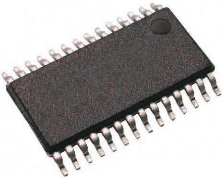
| 描述 | IC REG LDO 1.8V/3.3V 1A 28HTSSOP低压差稳压器 Dual-Output LDO Voltage Regulator |
| 产品分类 | |
| 品牌 | Texas Instruments |
| 产品手册 | |
| 产品图片 |
|
| rohs | 符合RoHS无铅 / 符合限制有害物质指令(RoHS)规范要求 |
| 产品系列 | 电源管理 IC,低压差稳压器,Texas Instruments TPS767D318PWP- |
| 数据手册 | |
| 产品型号 | TPS767D318PWP |
| 产品目录页面 | |
| 产品种类 | 低压差稳压器 |
| 供应商器件封装 | 28-HTSSOP |
| 其它名称 | 296-2741-5 |
| 包装 | 管件 |
| 单位重量 | 118.500 mg |
| 商标 | Texas Instruments |
| 回动电压—最大值 | 575 mV at 1 A |
| 安装类型 | 表面贴装 |
| 安装风格 | SMD/SMT |
| 封装 | Tube |
| 封装/外壳 | 28-SOIC(0.173",4.40mm 宽)裸露焊盘 |
| 封装/箱体 | HTSSOP-28 |
| 工作温度 | -40°C ~ 125°C |
| 工厂包装数量 | 50 |
| 最大功率耗散 | 5.07 W |
| 最大工作温度 | + 125 C |
| 最大输入电压 | 10 V |
| 最小工作温度 | - 40 C |
| 最小输入电压 | + 2.7 V |
| 标准包装 | 50 |
| 电压-跌落(典型值) | -,0.35V @ 1A |
| 电压-输入 | 2.7 V ~ 10 V |
| 电压-输出 | 1.8V,3.3V |
| 电压调节准确度 | 2 % |
| 电流-输出 | 1A |
| 电流-限制(最小值) | - |
| 稳压器拓扑 | 正,固定式 |
| 稳压器数 | 2 |
| 系列 | TPS767D318 |
| 线路调整率 | 0.01 % / V |
| 负载调节 | 3 mV |
| 输入偏压电流—最大 | 0.085 mA |
| 输出电压 | 1.8 V, 3.3 V |
| 输出电流 | 1 A |
| 输出端数量 | 2 Output |
| 输出类型 | Fixed |


- 商务部:美国ITC正式对集成电路等产品启动337调查
- 曝三星4nm工艺存在良率问题 高通将骁龙8 Gen1或转产台积电
- 太阳诱电将投资9.5亿元在常州建新厂生产MLCC 预计2023年完工
- 英特尔发布欧洲新工厂建设计划 深化IDM 2.0 战略
- 台积电先进制程称霸业界 有大客户加持明年业绩稳了
- 达到5530亿美元!SIA预计今年全球半导体销售额将创下新高
- 英特尔拟将自动驾驶子公司Mobileye上市 估值或超500亿美元
- 三星加码芯片和SET,合并消费电子和移动部门,撤换高东真等 CEO
- 三星电子宣布重大人事变动 还合并消费电子和移动部门
- 海关总署:前11个月进口集成电路产品价值2.52万亿元 增长14.8%


PDF Datasheet 数据手册内容提取
TPS767D3xx www.ti.com......................................................................................................................................................... SLVS209H–JULY1999–REVISEDAUGUST2008 DUAL-OUTPUT LOW-DROPOUT VOLTAGE REGULATORS FEATURES 1 • DualOutputVoltagesforSplit-Supply Because the PMOS device behaves as a low-value 23 Applications resistor, the dropout voltage is very low (350mV typically at an output current of 1A for the • OutputCurrentRangeof0mAto1.0Aper TPS767D325) and is directly proportional to the Regulator output current. Additionally, since the PMOS pass • 3.3V/2.5V,3.3V/1.8V,and3.3V/Adjustable element is a voltage-driven device, the quiescent Output current is very low and independent of output loading • Fast-TransientResponse (typically 85m A over the full range of output current, 0mA to 1A). These two key specifications yield a • 2%ToleranceOverLoadandTemperature significant improvement in operating life for • DropoutVoltageTypically350mVat1A battery-powered systems. This LDO family also • Ultra-low85m ATypicalQuiescentCurrent features a sleep mode; applying a TTL high signal to EN (enable) shuts down the regulator, reducing the • 1m AQuiescentCurrentDuringShutdown quiescentcurrentto1m AatT =+25°C. • DualOpen-DrainPower-OnResetwith200ms J The RESET output of the TPS767D3xx initiates a DelayforEachRegulator reset in microcomputer and microprocessor systems • 28-PinPowerPAD™TSSOPPackage in the event of an undervoltage condition. An internal • ThermalShutdownProtectionforEach comparator in the TPS767D3xx monitors the output Regulator voltage of the regulator to detect an undervoltage conditionontheregulatedoutputvoltage. DESCRIPTION The TPS767D3xx is offered in 1.8V, 2.5V, and 3.3V The TPS767D3xx family of dual voltage regulators fixed-voltage versions and in an adjustable version offers fast transient response, low dropout voltages (programmable over the range of 1.5V to 5.5V). and dual outputs in a compact package and Output voltage tolerance is specified as a maximum incorporating stability with 10m F low ESR output of 2% over line, load, and temperature ranges. The capacitors. TPS767D3xx family is available in a 28-pin PWP TSSOP package. They operate over a junction The TPS767D3xx family of dual voltage regulators is temperaturerangeof–40°Cto+125°C. designed primarily for DSP applications. These devices can be used in any mixed-output voltage application, with each regulator supporting up to 1A. Dual active-low reset signals allow resetting of core-logicandI/Oseparately. PWP PACKAGE (TOP VIEW) NC 1 28 1RESET V LINE TRANSIENT RESPONSE vs FDRREEO-PAOIRU TT EVMOPLETARGATEURE NC 2 27 NC D-VChange inOUT--VInput Voltage-Output VoltagemVIN -5411..000330 VCT2AOL0U==T 21=450 03°mC.F36V0 80100120140160180200 --VDropout VoltagemVDO11111001000--0-3221160VCOO-UU4TT0==- 312.003mVF0 20 40 II6OO0UUTTIO==8U 01T10A=1m 00A0120140 12GG211122ENNNNEIIIINNDCCDNNNN 1116479085231 22112122226479085321 N111NNN222FOOOORCCCCBUUUUE/STTTTNECT t-Time-ms TA-Free-Air Temperature-°C NC 13 16 NC NC 14 15 NC NC = No internal connection 1 Pleasebeawarethatanimportantnoticeconcerningavailability,standardwarranty,anduseincriticalapplicationsofTexas Instrumentssemiconductorproductsanddisclaimerstheretoappearsattheendofthisdatasheet. PowerPADisatrademarkofTexasInstruments. 2 Allothertrademarksarethepropertyoftheirrespectiveowners. 3 PRODUCTIONDATAinformationiscurrentasofpublicationdate. Copyright©1999–2008,TexasInstrumentsIncorporated Products conform to specifications per the terms of the Texas Instruments standard warranty. Production processing does not necessarilyincludetestingofallparameters.
TPS767D3xx SLVS209H–JULY1999–REVISEDAUGUST2008......................................................................................................................................................... www.ti.com This integrated circuit can be damaged by ESD. Texas Instruments recommends that all integrated circuits be handled with appropriateprecautions.Failuretoobserveproperhandlingandinstallationprocedurescancausedamage. ESDdamagecanrangefromsubtleperformancedegradationtocompletedevicefailure.Precisionintegratedcircuitsmaybemore susceptibletodamagebecauseverysmallparametricchangescouldcausethedevicenottomeetitspublishedspecifications. AVAILABLEOPTIONS(1) DEVICE REGULATOR1V (V) REGULATOR2V (V) OUT OUT TPS767D301 Adjustable(1.5V–5.5V) 3.3V TPS767D318 1.8V 3.3V TPS767D325 2.5V 3.3V (1) ForthemostcurrentspecificationsandpackageinformationseethePackageOptionAddendumattheendofthisdocument,orseethe TIwebsiteatwww.ti.com. ABSOLUTE MAXIMUM RATINGS(1) Overoperatingtemperaturerange(unlessotherwisenoted). TPS767D3xx UNIT Inputvoltagerange,V ,V (2) –0.3to+13.5 V 1IN 2IN Enablevoltagerange,V ,V –0.3toV +0.3 V 1EN 2EN IN Outputvoltagerange,V ,V –0.3to+7.0 V 1OUT 2OUT RESETvoltagerange,V ,V –0.3to+16.5 V 1RESET 2RESET Peakoutputcurrent Internallylimited ESDrating,HBM 2 kV Continuoustotalpowerdissipation SeeDissipationRatingstable Operatingjunctiontemperaturerange,T –40to+125 °C J Storagetemperaturerange,T –65to+150 °C stg (1) Stressesbeyondthoselistedunderabsolutemaximumratingsmaycausepermanentdamagetothedevice.Thesearestressratings only,andfunctionaloperationofthedeviceattheseoranyotherconditionsbeyondthoseindicatedunderrecommendedoperating conditionsisnotimplied.Exposuretoabsolute-maximum-ratedconditionsforextendedperiodsmayaffectdevicereliability. (2) Allvoltagevaluesarewithrespecttonetworkterminalground. POWER DISSIPATION RATINGS AIRFLOW T ≤+25°C DERATINGFACTOR T =+70°C T =+85°C A A A PACKAGE (CFM) POWERRATING ABOVEt =+25°C POWERRATING POWERRATING a 0 3.58W 35.8mW/°C 1.97W 1.43W PWP(1) 250 5.07W 50.7mW/°C 2.79W 2.03W (1) Thisparameterismeasuredwiththerecommendedcopperheatsinkpatternona4-layerPCB,1oz.copperon4-in×4-ingroundlayer. Formoreinformation,refertoTItechnicalbriefliteraturenumberSLMA002. 2 SubmitDocumentationFeedback Copyright©1999–2008,TexasInstrumentsIncorporated
TPS767D3xx www.ti.com......................................................................................................................................................... SLVS209H–JULY1999–REVISEDAUGUST2008 ELECTRICAL CHARACTERISTICS Overoperatingtemperaturerange(T =–40°Cto+125°C),V =V +1V,I =1mA,V =0V,and J IN OUT(nom) OUT EN C =10m F,unlessotherwisenoted.AdjustablechannelsaresettoV =3.3V.TypicalvaluesareatT =25°C. OUT OUT J PARAMETER TESTCONDITIONS MIN TYP MAX UNIT V Inputvoltagerange,V ,V (1) 2.7 10 V IN 1IN 2IN AdjustableV range,V ,V 1.5 5.5 V OUT 1OUT 2OUT V Accuracy,adjustableVOUTchannels(1) V10OUm TA+≤1IV≤V≤IN1A≤5.5V; –2.0 +2.0 % OUT OUT Accuracy,fixedVOUTchannels(1) V10OUm TA+≤1IV≤V≤IN1A≤10V; –2.0 +2.0 % OUT ΔV %/ΔV Lineregulation(1) V +1.0V≤V ≤10V 0.01 %/V OUT IN OUT IN ΔV %/ΔI Loadregulation 10m A≤I ≤1A 3 mV OUT OUT OUT Dropoutvoltage(2) V V =3.3V,I =1A 350 575 mV DO (V =V (nom)–0.1V) OUT OUT IN OUT I Outputcurrentlimit,perLDO V =0V,T =+25°C 1.7 2 A CL OUT J I Groundpincurrent,perLDO 10m A≤I ≤1A 85 125 m A GND OUT I Standbycurrent,perLDO 2.7V≤V ≤10V,V =V 1 10 m A SHDN IN EN IN I FBcurrentinput(Adjustable) V =1.5V 2 nA FB FB PSRR Power-supplyripplerejection f=1kHz,C =10m F 60 dB OUT VN Outputnoisevoltage BI W==1A2,0C0Hzto=11000m kFHz,VOUT=1.8V, 55 m VRMS C OUT V High-levelenableinputvoltage T =+25°C 2.0 V EN(HI) J V Low-levelenableinputvoltage T =+25°C 0.8 V EN(LO) J V =0V,T =+25°C –1 0 1 I Inputcurrent EN J m A EN V =V ,T =+25°C –1 1 EN IN J Minimuminputvoltageforvalid I =300m A 1.1 V RESET OUT(RESET) Tripthresholdvoltage V decreasing,T =+25°C 92 98 %V OUT J OUT Hysteresisvoltage MeasuredatV 0.5 %V OUT OUT Reset V =2.7V,T =+25°C, Outputlowvoltage I J 0.15 0.4 V I =1mA OUT(RESET) Leakagecurrent V =7V,T =+25°C 1 m A (RESET) J RESETtime-outdelay T =+25°C 100 200 400 ms J T Thermalshutdowntemperature 150 °C SD T Operatingjunctiontemperature –40 +125 °C J (1) MinimumV =V +V or2.7V,whicheverisgreater. IN OUT DO (2) Dropoutvoltage(V )isnotmeasuredforchannelswithV <2.8VsinceminimumV =2.7V. DO OUT(nom) IN Copyright©1999–2008,TexasInstrumentsIncorporated SubmitDocumentationFeedback 3
TPS767D3xx SLVS209H–JULY1999–REVISEDAUGUST2008......................................................................................................................................................... www.ti.com FUNCTIONALBLOCKDIAGRAM—FixedVoltageVersion(oneregulatorchannel) IN EN RESET OUT 200ms Delay V = REF 1.1834V R1 R 2 GND FUNCTIONALBLOCKDIAGRAM—AdjustableVersion(oneregulatorchannel) IN EN RESET OUT 200ms Delay V = REF 1.1834V R1 FB/NC R 2 External to GND the device 4 SubmitDocumentationFeedback Copyright©1999–2008,TexasInstrumentsIncorporated
TPS767D3xx www.ti.com......................................................................................................................................................... SLVS209H–JULY1999–REVISEDAUGUST2008 PWP PACKAGE (TOP VIEW) NC 1 28 1RESET NC 2 27 NC 1GND 3 26 NC 1EN 4 25 1FB/NC 1IN 5 24 1OUT 1IN 6 23 1OUT NC 7 22 2RESET NC 8 21 NC 2GND 9 20 NC 2EN 10 19 NC 2IN 11 18 2OUT 2IN 12 17 2OUT NC 13 16 NC NC 14 15 NC NC = No internal connection TERMINALFUNCTIONS TERMINAL DESCRIPTION NAME NO. 1GND 3 Regulator#1ground 1EN 4 Regulator#1enable 1IN 5,6 Regulator#1inputsupplyvoltage 2GND 9 Regulator#2ground 2EN 10 Regulator#2enable 2IN 11,12 Regulator#2inputsupplyvoltage 2OUT 17,18 Regulator#2outputvoltage 2RESET 22 Regulator#2resetsignal 1OUT 23,24 Regulator#1outputvoltage 1FB/NC 25 Regulator#1outputvoltagefeedbackforadjustableoutput;noconnectionforfixedoutput 1RESET 28 Regulator#1resetsignal NC 1,2,7,8, Nointernalconnection 13–16,19, 20,21,26, 27 Copyright©1999–2008,TexasInstrumentsIncorporated SubmitDocumentationFeedback 5
TPS767D3xx SLVS209H–JULY1999–REVISEDAUGUST2008......................................................................................................................................................... www.ti.com TPS767D3xx 5 28 VIN IN RESET RESET 6 IN 250kW 24 OUT V OUT 0.1mCF1 4 EN OUT 23 + C 50V OUT 10mF GND 3 Figure1.TypicalApplicationCircuit(FixedVersions)forSingleChannel TIMING DIAGRAM V IN VRES(1) VRES t VOUT V +(2) V +(2) IT IT Threshold Voltage Less than 5% of V - the output voltage V - IN IN t RESET 200ms 200ms Output Delay Delay Output Output Undefined Undefined t (1) V istheminimuminputvoltageforavalidRESET. RES (2) V —Tripvoltageistypically5%lowerthantheoutputvoltage(95%V ). IT OUT 6 SubmitDocumentationFeedback Copyright©1999–2008,TexasInstrumentsIncorporated
TPS767D3xx www.ti.com......................................................................................................................................................... SLVS209H–JULY1999–REVISEDAUGUST2008 TYPICAL CHARACTERISTICS OUTPUTVOLTAGE OUTPUTVOLTAGE OUTPUTVOLTAGE vs vs vs OUTPUTCURRENT OUTPUTCURRENT OUTPUTCURRENT 3.2835 1.7965 2.4960 VOUT= 3.3V VOUT= 1.8V VOUT= 2.5V 3.2830 VTAIN== +42.35V°C VTAIN==+ 22.58°VC 2.4955 VTAIN== +32.55V°C 1.7960 -V 3.2825 -V -V 2.4950 -Output Voltage 33..22881250 -Output Voltage11..77995550 -Output Voltage 222...444999443055 VOUT 3.2810 VOUT VOUT 2.4930 1.7945 3.2805 2.4925 3.2800 1.7940 2.4920 0 0.1 0.2 0.3 0.4 0.5 0.6 0.7 0.8 0.9 1 0 0.1 0.2 0.3 0.4 0.5 0.6 0.7 0.8 0.9 1 0 0.1 0.2 0.3 0.4 0.5 0.6 0.7 0.8 0.9 1 IOUT-Output Current-A IOUT-Output Current-A IOUT-Output Current-A Figure2. Figure3. Figure4. OUTPUTVOLTAGE OUTPUTVOLTAGE OUTPUTVOLTAGE vs vs vs FREE-AIRTEMPERATURE FREE-AIRTEMPERATURE FREE-AIRTEMPERATURE 3.32 1.815 2.515 VOUT= 3.3V VOUT= 1.8V VOUT= 2.5V 3.31 VIN= 4.3V VIN= 2.8V 2.510 VIN= 3.5V 1.810 -V 3.30 -V -V 2.505 ge ge 1.805 ge Output Volta 33..2289 IOUT= 1A IOUT= 1mA Output Volta 1.800 IOUT= 1A I = 1mA Output Volta 22..540905 IOUT= 1A -VOUT 3.27 -VOUT 1.795 OUT -VOUT 2.490 IOUT= 1mA 1.790 3.26 2.485 3.25 1.785 2.480 −60−40 −20 0 20 40 60 80 100 120 140 −60−40 −20 0 20 40 60 80 100 120 140 −60 −40 −20 0 20 40 60 80 100 120 TA-Free-Air Temperature-°C TA-Free-Air Temperature-°C TA-Free-Air Temperature-°C Figure5. Figure6. Figure7. GROUNDCURRENT GROUNDCURRENT POWERSUPPLYRIPPLEREJECTION vs vs vs FREE-AIRTEMPERATURE FREE-AIRTEMPERATURE FREQUENCY 92 96 90 90 VVOINU=T =4 .33.V3V 94 VVOINU=T =2 .18.V8V -dB 80 VVCOINU=T ==4 .313.0V3mVF Ground CurrentA- m 788888848206 IOUT= 1A IOUT= 1mA Ground CurrentA- m 899888620428 IOUT= 1mAIOUT= 500mA wer-Supply Ripple Rejection 765432000000 ITOAOUUT=T= + 12A5°C 76 IOUT= 500mA 80 -Po 10 78 R R 74 76 PS 0 I = 1A 72−60−40 −20 0 20 40 60 80 100 120 140 74−60−40OUT−20 0 20 40 60 80 100 120 140 −1010 100 1k 10k 100k 1M f-Frequency-Hz TA-Free-Air Temperature-°C TA-Free-Air Temperature-°C Figure8. Figure9. Figure10. Copyright©1999–2008,TexasInstrumentsIncorporated SubmitDocumentationFeedback 7
TPS767D3xx SLVS209H–JULY1999–REVISEDAUGUST2008......................................................................................................................................................... www.ti.com TYPICAL CHARACTERISTICS (continued) OUTPUTSPECTRALNOISEDENSITY OUTPUTIMPEDANCE DROPOUTVOLTAGE vs vs vs FREQUENCY FREQUENCY FREE-AIRTEMPERATURE 10−5 0 103 VIN= 4.3V VIN= 4.3V -ÖOutput Spectral Noise DensityV/Hz 1100−−67 IOUT= 1AIOUT= 7mACTAOU=T +=2 150°mCF --WZOutput ImpedanceOUT10−1 CTAOIUO=TU T2=5= 1° 1C0mmFA IOUT= 1A --VDropout VoltagemVDO 11110000−2101 IOUT=IO 1U0Tm= A1A -Vn VOUT= 3.3V IOUT= 0 C = 10mF 10−8 10−2 10−2 OUT 102 103 104 105 101 102 103 104 105 106 −60 −40 −20 0 20 40 60 80 100 120 140 f-Frequency-Hz f-Frequency-Hz TA-Free-Air Temperature-°C Figure11. Figure12. Figure13. LINETRANSIENTRESPONSE LOADTRANSIENTRESPONSE LINETRANSIENTRESPONSE 100 --VInput VoltageVI 32..88 VIOUT== 1 10.m8VA D-VChange inO-Output VoltagemV −55000 VVCTAOIONUU==TT +==22 .1185.0V°80CVmF --VInput VoltageVI 5.3 VCTAOOUU=TT +==2 315.0°3mCVF COOUUTT= 10mF A −100 V 4.3 D-VChange inO-Output VoltagemV −22000 TA= +25°C --IOutput CurrentO 0.105 D-VChange inO-Output Voltagem −11000 0 20 40 60 80 100 120 140 160 180 200 0 20 40 60 80 100 120 140 160 180 200 0 20 40 60 80 100 120 140 160 180 200 t-Time- ms t-Time- ms t-Time- ms Figure14. Figure15. Figure16. OUTPUTVOLTAGE DROPOUTVOLTAGE vs vs LOADTRANSIENTRESPONSE TIME(ATSTART-UP) INPUTVOLTAGE 100 4 900 D-VChange inO-Output VoltagemV −55000 VCTAOOUU=TT +==2 315.0°30CVmF --Output VoltageV 321 -VoltagemV 687000000 IOUT= 1A -entA −1001 V-VO 0 -Dropout 540000 TA= +25°C TA= +125°C utput Curr 0.05 ble Pulse VDO 320000 TA=-40°C -O Ena 0 100 IO 0 20 40 60 80 100 120 140 160 180 200 02.5 3 3.5 4 4.5 5 t-Time- ms 0 20 40 60 80 100 120 140 160 180 200 V-Input Voltage-V t-Time- ms I Figure17. Figure18. Figure19. 8 SubmitDocumentationFeedback Copyright©1999–2008,TexasInstrumentsIncorporated
TPS767D3xx www.ti.com......................................................................................................................................................... SLVS209H–JULY1999–REVISEDAUGUST2008 VIN IN To Load OUT + EN COUT GND RL ESR Figure20.TestCircuitforTypicalRegionsofStability(Figure21throughFigure24) (FixedOutputOptions) Equivalent series resistance (ESR) refers to the total series resistance, including the ESR of the capacitor, any resistanceaddedexternally,andPWBtraceresistancetoC . OUT TYPICALREGIONOFSTABILITY TYPICALREGIONOFSTABILITY ESRvsOUTPUTCURRENT ESRvsOUTPUTCURRENT 10 10 Region of Instability W Region of Instability W - - e e c c n n a a st 1 st 1 nt Series Resi VCVTAOIONUU==TT +==42 .3435..V°37CVmF Region of Stability nt Series Resi VCVTAOIONUU==TT +==41 .3432..V537°VmCF Region of Stability ale 0.1 ale 0.1 v v ui ui q q E E - - R R S Region of Instability S Region of Instability E E 0.01 0.01 0 200 400 600 800 1000 0 200 400 600 800 1000 IOUT-Output Current-mA IOUT-Output Current-mA Figure21. Figure22. TYPICALREGIONOFSTABILITY TYPICALREGIONOFSTABILITY ESRvsOUTPUTCURRENT ESRvsOUTPUTCURRENT 10 10 Region of Instability W Region of Instability W - - e e c c n n a a sist 1 sist 1 alent Series Re 0.1 VCVTAOIONUU==TT +==42 .3235.2V°3mCVF Region of Stability alent Series Re 0.1 VCVTAOIONUU==TT +==41 .3232.2V53m°VCF Region of Stability v v ui ui q q E E - - R R ES Region of Instability ES Region of Instability 0.01 0.01 0 200 400 600 800 1000 0 200 400 600 800 1000 I -Output Current-mA I -Output Current-mA OUT OUT Figure23. Figure24. Copyright©1999–2008,TexasInstrumentsIncorporated SubmitDocumentationFeedback 9
TPS767D3xx SLVS209H–JULY1999–REVISEDAUGUST2008......................................................................................................................................................... www.ti.com APPLICATION INFORMATION ThefeaturesoftheTPS767D3xxfamily(low-dropoutvoltage,ultralowquiescent current, power-saving shutdown mode, and a supply-voltage supervisor) and the power-dissipation properties of the TSSOP PowerPAD package have enabled the integration of the dual LDO regulator with high output current for use in DSP and other multiple voltageapplications.Figure25showsatypicaldual-voltageDSPapplication. U1 R R TPS767D325 1 2 100kW 100kW PG 1 NC 1RESET 28 2 NC NC 27 RESETto DSP 3 1GND NC 26 4 1EN 1FB/NC 25 5 1IN 1OUT 24 5V DSP 6 1IN 1OUT 23 2.5V V CORE C0 7 NC 2RESET 22 1mF 8 NC NC 21 9 2GND NC 20 10 2EN NC 19 11 2IN 2OUT 18 +C3 12 2IN 2OUT 17 33mF 13 NC NC 16 14 NC NC 15 3.3V V I/O C C 1 2 1mF 33mF GND GND Figure25.Dual-VoltageDSPApplication DSP power requirements include very high transient currents that must be considered in the initial design. This designuseshigher-valuedoutputcapacitorstohandlethelargetransientcurrents. DEVICE OPERATION The TPS767D3xx features very low quiescent current, which remain virtually constant even with varying loads. Conventional LDO regulators use a pnp pass element, the base current of which is directly proportional to the loadcurrentthroughthe regulator (I = I /b ). Close examination of the data sheets reveals that these devices are B C typically specified under near no-load conditions; actual operating currents are much higher as evidenced by typical quiescent current versus load current curves. The TPS767D3xx uses a PMOS transistor to pass current; because the gate of the PMOS is voltage driven, operating current is low and invariable over the full load range. TheTPS767D3xxspecificationsreflectactualperformanceunderloadcondition. Another pitfall associated with the pnp pass element is its tendency to saturate when the device goes into dropout. The resulting drop in b forces an increase in I to maintain the load. During power-up, this translates to B large start-up currents. Systems with limited supply current may fail to start up. In battery-powered systems, it means rapid battery discharge when the voltage decays below the minimum required for regulation. The TPS767D3xxquiescentcurrentremainslowevenwhentheregulatordropsout,eliminatingbothproblems. 10 SubmitDocumentationFeedback Copyright©1999–2008,TexasInstrumentsIncorporated
TPS767D3xx www.ti.com......................................................................................................................................................... SLVS209H–JULY1999–REVISEDAUGUST2008 The TPS767D3xx family also features a shutdown mode that places the output in the high-impedance state (essentially equal to the feedback-divider resistance) and reduces quiescent current to under 2m A. If the shutdown feature is not used, EN should be tied to ground. Response to an enable transition is quick; regulated outputvoltageistypicallyre-establishedin120m s. MINIMUM LOAD REQUIREMENTS TheTPS767D3xxfamilyisstableevenatzeroload;nominimumloadisrequiredforoperation. FB-PIN CONNECTION (ADJUSTABLE VERSION ONLY) The FB pin is an input pin to sense the output voltage and close the loop for the adjustable option. The output voltage is sensed through a resistor divider network as is shown in Figure 26 to close the loop. Normally, this connection should be as short as possible; however, the connection can be made near a critical circuit to improve performance at that point. Internally, FB connects to a high-impedance, wide-bandwidth amplifier and noise pickup feeds through to the regulator output. Routing the FB connection to minimize/avoid noise pickup is essential.Infixedoutputoptions,thispinisnotconnected. EXTERNAL CAPACITOR REQUIREMENTS An input capacitor is not required; however, a ceramic bypass capacitor (0.047pF to 0.1m F) improves load transient response and noise rejection when the TPS767D3xx is located more than a few inches from the power supply. A higher-capacitance electrolytic capacitor may be necessary if large (hundreds of milliamps) load transientswithfastrisetimesareanticipated. Like all low dropout regulators, the TPS767D3xx requires an output capacitor connected between OUT and GND to stabilize the internal control loop. The minimum recommended capacitance value is 10m F and the ESR (equivalent series resistance) must be between 60mΩ and 1.5Ω. Capacitor values of 10m F or larger are acceptable, provided the ESR is less than 1.5Ω. Solid tantalum electrolytic, aluminum electrolytic, and multilayer ceramiccapacitorsareallsuitable,providedtheymeettherequirementsdescribedpreviously. When necessary to achieve low height requirements along with high output current and/or high ceramic load capacitance,severalhigherESRcapacitorscanbeusedinparalleltomeetthepreviousguidelines. PROGRAMMING THE TPS767D301 ADJUSTABLE LDO REGULATOR The output voltage of the TPS767D301 adjustable regulator is programmed using an external resistor divider as showninFigure26.Theoutputvoltageiscalculatedusing: (cid:4) R (cid:5) VOUT(cid:3)VREF(cid:1) 1(cid:2)R1 2 (1) ResistorsR andR shouldbechosenforapproximately40m Adivider current. Lower-value resistors can be used 1 2 but offer no inherent advantage and waste more power. Higher values should be avoided as leakage currents at FBincreasetheoutputvoltageerror. Copyright©1999–2008,TexasInstrumentsIncorporated SubmitDocumentationFeedback 11
TPS767D3xx SLVS209H–JULY1999–REVISEDAUGUST2008......................................................................................................................................................... www.ti.com The recommended design procedure is to choose R = 30.1kΩ to set the divider current at 40m A and then 2 calculateR using: 1 (cid:4)V (cid:5) R1(cid:3) VOUT(cid:2)1 (cid:1)R2 REF (2) TPS767D301 OUTPUT VOLTAGE VIN IN RESET RESETOutput PROGRAMMING GUIDE OUTPUT 0.1mF 250kW VOLTAGE R1 R2 UNIT > 2.7V OUT VOUT 2.5V 33.2 30.1 kW R 3.3V 53.6 30.1 kW EN 1 < 0.5V FB/NC + COUT 3.6V 61.9 30.1 kW 10mF GND R2 4.75V 90.8 30.1 kW Figure26.TPS767D301AdjustableLDORegulatorProgramming RESET INDICATOR The TPS767D3xx features a RESET output that can be used to monitor the status of the regulator. The internal comparator monitors the output voltage: when the output drops to 95% (typical) of its regulated value, the RESET output transistor turns on, taking the signal low. The open-drain output requires a pullup resistor. If not used,itcanbeleftfloating.RESETcanbeusedtodrivepower-onresetcircuitryorasalow-batteryindicator. REGULATOR PROTECTION The TPS767D3xx PMOS-pass transistor has a built-in back-gate diode that safely conducts reverse currents when the input voltage drops below the output voltage (for example, during power-down). Current is conducted from the output to the input and is not internally limited. When extended reverse voltage is anticipated, external limitingmaybeappropriate. The TPS767D3xx also features internal current limiting and thermal protection. During normal operation, the TPS767D3xx limits output current to approximately 1.7A. When current limiting engages, the output voltage scales back linearly until the overcurrent condition ends. While current limiting is designed to prevent gross device failure, care should be taken not to exceed the power dissipation ratings of the package. If the temperature of the device exceeds +150°C (typ), thermal-protection circuitry shuts it down. Once the device has cooledbelow+130°C(typ),regulatoroperationresumes. 12 SubmitDocumentationFeedback Copyright©1999–2008,TexasInstrumentsIncorporated
TPS767D3xx www.ti.com......................................................................................................................................................... SLVS209H–JULY1999–REVISEDAUGUST2008 POWER DISSIPATION AND JUNCTION TEMPERATURE Specified regulator operation is assured to a junction temperature of +125°C; the maximum junction temperature should be restricted to +125°C under normal operating conditions. This restriction limits the power dissipation the regulator can handle in any given application. To ensure the junction temperature is within acceptable limits, calculate the maximum allowable dissipation, P max, and the actual dissipation, P , which must be less than or D D equaltoP max. D Themaximum-power-dissipationlimitisdeterminedusingthefollowingequation: T max(cid:1)T P max(cid:2) J A D R (cid:1)JA (3) Where: • T maxisthemaximumallowablejunctiontemperature. J • Rq JA is the thermal resistance junction-to-ambient for the package, that is, 28°C/W for the 28-terminal PWP withnoairflow. • T istheambienttemperature. A Theregulatordissipationiscalculatedusing: PD(cid:3)(cid:4)VIN(cid:2)VOUT(cid:5)(cid:1)IOUT (4) Power dissipation resulting from quiescent current is negligible. Excessive power dissipation will trigger the thermalprotectioncircuit. Copyright©1999–2008,TexasInstrumentsIncorporated SubmitDocumentationFeedback 13
TPS767D3xx SLVS209H–JULY1999–REVISEDAUGUST2008......................................................................................................................................................... www.ti.com Revision History ChangesfromRevisionF(February2008)toRevisionG ............................................................................................. Page • ChangedCorrectedsymbolforFBcurrentinElectricalCharacteristics................................................................................ 3 14 SubmitDocumentationFeedback Copyright©1999–2008,TexasInstrumentsIncorporated
PACKAGE OPTION ADDENDUM www.ti.com 6-Feb-2020 PACKAGING INFORMATION Orderable Device Status Package Type Package Pins Package Eco Plan Lead/Ball Finish MSL Peak Temp Op Temp (°C) Device Marking Samples (1) Drawing Qty (2) (6) (3) (4/5) TPS767D301PWP ACTIVE HTSSOP PWP 28 50 Green (RoHS NIPDAU Level-2-260C-1 YEAR -40 to 125 PS767D301 & no Sb/Br) TPS767D301PWPG4 ACTIVE HTSSOP PWP 28 50 Green (RoHS NIPDAU Level-2-260C-1 YEAR -40 to 125 PS767D301 & no Sb/Br) TPS767D301PWPR ACTIVE HTSSOP PWP 28 2000 Green (RoHS NIPDAU Level-2-260C-1 YEAR -40 to 125 PS767D301 & no Sb/Br) TPS767D301PWPRG4 ACTIVE HTSSOP PWP 28 2000 Green (RoHS NIPDAU Level-2-260C-1 YEAR -40 to 125 PS767D301 & no Sb/Br) TPS767D318PWP ACTIVE HTSSOP PWP 28 50 Green (RoHS NIPDAU Level-2-260C-1 YEAR -40 to 125 PS767D318 & no Sb/Br) TPS767D318PWPG4 ACTIVE HTSSOP PWP 28 50 Green (RoHS NIPDAU Level-2-260C-1 YEAR -40 to 125 PS767D318 & no Sb/Br) TPS767D318PWPR ACTIVE HTSSOP PWP 28 2000 Green (RoHS NIPDAU Level-2-260C-1 YEAR -40 to 125 PS767D318 & no Sb/Br) TPS767D325PWP ACTIVE HTSSOP PWP 28 50 Green (RoHS NIPDAU Level-2-260C-1 YEAR -40 to 125 PS767D325 & no Sb/Br) TPS767D325PWPG4 ACTIVE HTSSOP PWP 28 50 Green (RoHS NIPDAU Level-2-260C-1 YEAR -40 to 125 PS767D325 & no Sb/Br) TPS767D325PWPR ACTIVE HTSSOP PWP 28 2000 Green (RoHS NIPDAU Level-2-260C-1 YEAR -40 to 125 PS767D325 & no Sb/Br) (1) The marketing status values are defined as follows: ACTIVE: Product device recommended for new designs. LIFEBUY: TI has announced that the device will be discontinued, and a lifetime-buy period is in effect. NRND: Not recommended for new designs. Device is in production to support existing customers, but TI does not recommend using this part in a new design. PREVIEW: Device has been announced but is not in production. Samples may or may not be available. OBSOLETE: TI has discontinued the production of the device. (2) RoHS: TI defines "RoHS" to mean semiconductor products that are compliant with the current EU RoHS requirements for all 10 RoHS substances, including the requirement that RoHS substance do not exceed 0.1% by weight in homogeneous materials. Where designed to be soldered at high temperatures, "RoHS" products are suitable for use in specified lead-free processes. TI may reference these types of products as "Pb-Free". RoHS Exempt: TI defines "RoHS Exempt" to mean products that contain lead but are compliant with EU RoHS pursuant to a specific EU RoHS exemption. Green: TI defines "Green" to mean the content of Chlorine (Cl) and Bromine (Br) based flame retardants meet JS709B low halogen requirements of <=1000ppm threshold. Antimony trioxide based flame retardants must also meet the <=1000ppm threshold requirement. (3) MSL, Peak Temp. - The Moisture Sensitivity Level rating according to the JEDEC industry standard classifications, and peak solder temperature. Addendum-Page 1
PACKAGE OPTION ADDENDUM www.ti.com 6-Feb-2020 (4) There may be additional marking, which relates to the logo, the lot trace code information, or the environmental category on the device. (5) Multiple Device Markings will be inside parentheses. Only one Device Marking contained in parentheses and separated by a "~" will appear on a device. If a line is indented then it is a continuation of the previous line and the two combined represent the entire Device Marking for that device. (6) Lead/Ball Finish - Orderable Devices may have multiple material finish options. Finish options are separated by a vertical ruled line. Lead/Ball Finish values may wrap to two lines if the finish value exceeds the maximum column width. Important Information and Disclaimer:The information provided on this page represents TI's knowledge and belief as of the date that it is provided. TI bases its knowledge and belief on information provided by third parties, and makes no representation or warranty as to the accuracy of such information. Efforts are underway to better integrate information from third parties. TI has taken and continues to take reasonable steps to provide representative and accurate information but may not have conducted destructive testing or chemical analysis on incoming materials and chemicals. TI and TI suppliers consider certain information to be proprietary, and thus CAS numbers and other limited information may not be available for release. In no event shall TI's liability arising out of such information exceed the total purchase price of the TI part(s) at issue in this document sold by TI to Customer on an annual basis. OTHER QUALIFIED VERSIONS OF TPS767D3 : •Automotive: TPS767D3-Q1 NOTE: Qualified Version Definitions: •Automotive - Q100 devices qualified for high-reliability automotive applications targeting zero defects Addendum-Page 2
PACKAGE MATERIALS INFORMATION www.ti.com 20-Feb-2019 TAPE AND REEL INFORMATION *Alldimensionsarenominal Device Package Package Pins SPQ Reel Reel A0 B0 K0 P1 W Pin1 Type Drawing Diameter Width (mm) (mm) (mm) (mm) (mm) Quadrant (mm) W1(mm) TPS767D301PWPR HTSSOP PWP 28 2000 330.0 16.4 6.9 10.2 1.8 12.0 16.0 Q1 TPS767D318PWPR HTSSOP PWP 28 2000 330.0 16.4 6.9 10.2 1.8 12.0 16.0 Q1 TPS767D325PWPR HTSSOP PWP 28 2000 330.0 16.4 6.9 10.2 1.8 12.0 16.0 Q1 PackMaterials-Page1
PACKAGE MATERIALS INFORMATION www.ti.com 20-Feb-2019 *Alldimensionsarenominal Device PackageType PackageDrawing Pins SPQ Length(mm) Width(mm) Height(mm) TPS767D301PWPR HTSSOP PWP 28 2000 350.0 350.0 43.0 TPS767D318PWPR HTSSOP PWP 28 2000 350.0 350.0 43.0 TPS767D325PWPR HTSSOP PWP 28 2000 350.0 350.0 43.0 PackMaterials-Page2
GENERIC PACKAGE VIEW PWP 28 PowerPADTM TSSOP - 1.2 mm max height 4.4 x 9.7, 0.65 mm pitch SMALL OUTLINE PACKAGE Images above are just a representation of the package family, actual package may vary. Refer to the product data sheet for package details. 4224765/A www.ti.com
None
None
None
IMPORTANTNOTICEANDDISCLAIMER TI PROVIDES TECHNICAL AND RELIABILITY DATA (INCLUDING DATASHEETS), DESIGN RESOURCES (INCLUDING REFERENCE DESIGNS), APPLICATION OR OTHER DESIGN ADVICE, WEB TOOLS, SAFETY INFORMATION, AND OTHER RESOURCES “AS IS” AND WITH ALL FAULTS, AND DISCLAIMS ALL WARRANTIES, EXPRESS AND IMPLIED, INCLUDING WITHOUT LIMITATION ANY IMPLIED WARRANTIES OF MERCHANTABILITY, FITNESS FOR A PARTICULAR PURPOSE OR NON-INFRINGEMENT OF THIRD PARTY INTELLECTUAL PROPERTY RIGHTS. These resources are intended for skilled developers designing with TI products. You are solely responsible for (1) selecting the appropriate TI products for your application, (2) designing, validating and testing your application, and (3) ensuring your application meets applicable standards, and any other safety, security, or other requirements. These resources are subject to change without notice. TI grants you permission to use these resources only for development of an application that uses the TI products described in the resource. Other reproduction and display of these resources is prohibited. No license is granted to any other TI intellectual property right or to any third party intellectual property right. TI disclaims responsibility for, and you will fully indemnify TI and its representatives against, any claims, damages, costs, losses, and liabilities arising out of your use of these resources. TI’s products are provided subject to TI’s Terms of Sale (www.ti.com/legal/termsofsale.html) or other applicable terms available either on ti.com or provided in conjunction with such TI products. TI’s provision of these resources does not expand or otherwise alter TI’s applicable warranties or warranty disclaimers for TI products. Mailing Address: Texas Instruments, Post Office Box 655303, Dallas, Texas 75265 Copyright © 2020, Texas Instruments Incorporated