ICGOO在线商城 > 集成电路(IC) > PMIC - 稳压器 - 线性 > TPS76318DBVR
 Datasheet下载
- 型号: TPS76318DBVR
- 制造商: Texas Instruments
- 库位|库存: xxxx|xxxx
- 要求:
| 数量阶梯 | 香港交货 | 国内含税 |
| +xxxx | $xxxx | ¥xxxx |
查看当月历史价格
查看今年历史价格
TPS76318DBVR产品简介:
ICGOO电子元器件商城为您提供TPS76318DBVR由Texas Instruments设计生产,在icgoo商城现货销售,并且可以通过原厂、代理商等渠道进行代购。 TPS76318DBVR价格参考。Texas InstrumentsTPS76318DBVR封装/规格:PMIC - 稳压器 - 线性, Linear Voltage Regulator IC 1 Output 150mA SOT-23-5。您可以下载TPS76318DBVR参考资料、Datasheet数据手册功能说明书,资料中有TPS76318DBVR 详细功能的应用电路图电压和使用方法及教程。
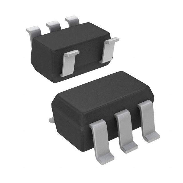
TPS76318DBVR是Texas Instruments(德州仪器)生产的一款低压差线性稳压器(LDO),输出电压为1.8V,最大输出电流可达150mA,采用SOT-23-5小型封装。该器件具有低静态电流、高电源抑制比(PSRR)和良好的负载/线路调节能力,适合对噪声敏感和空间受限的应用。

典型应用场景包括:

1. 便携式电子设备:如智能手机、平板电脑和可穿戴设备,用于为微处理器、传感器或低功耗MCU供电,其低静态电流有助于延长电池寿命。

2. 嵌入式系统与微控制器供电:为ARM Cortex-M系列、MSP430等低功耗MCU提供稳定、干净的1.8V电源,确保系统可靠运行。

3. 通信模块:适用于Wi-Fi、蓝牙、ZigBee等无线模块的电源管理,LDO的低噪声特性有助于减少对射频信号的干扰。

4. 工业控制与传感器接口:在PLC、数据采集系统中为精密模拟电路(如ADC、传感器信号调理电路)供电,提升系统精度和稳定性。

5. 消费类电子产品:如数码相机、音频设备中的数字逻辑电路或存储器供电。

TPS76318DBVR工作输入电压范围宽(2.7V至6.5V),集成过温保护和短路保护功能,可靠性高,适合在噪声敏感、空间紧凑且要求高效稳定的电源设计中使用。
| 参数 | 数值 |
| 产品目录 | 集成电路 (IC)半导体 |
| 描述 | IC REG LDO 1.8V 0.15A SOT23-5低压差稳压器 Low-Power 150-mA |
| 产品分类 | |
| 品牌 | Texas Instruments |
| 产品手册 | |
| 产品图片 |
|
| rohs | 符合RoHS无铅 / 符合限制有害物质指令(RoHS)规范要求 |
| 产品系列 | 电源管理 IC,低压差稳压器,Texas Instruments TPS76318DBVR- |
| 数据手册 | |
| 产品型号 | TPS76318DBVR |
| PCN设计/规格 | |
| 产品种类 | 低压差稳压器 |
| 供应商器件封装 | SOT-23-5 |
| 其它名称 | 296-11016-6 |
| 包装 | Digi-Reel® |
| 单位重量 | 13 mg |
| 商标 | Texas Instruments |
| 安装类型 | 表面贴装 |
| 安装风格 | SMD/SMT |
| 封装 | Reel |
| 封装/外壳 | SC-74A,SOT-753 |
| 封装/箱体 | SOT-23-5 |
| 工作温度 | -40°C ~ 125°C |
| 工厂包装数量 | 3000 |
| 最大功率耗散 | 0.555 W |
| 最大工作温度 | + 125 C |
| 最大输入电压 | 10 V |
| 最小工作温度 | - 40 C |
| 最小输入电压 | + 2.7 V |
| 标准包装 | 1 |
| 电压-跌落(典型值) | - |
| 电压-输入 | 2.7 V ~ 10 V |
| 电压-输出 | 1.8V |
| 电压调节准确度 | 3 % |
| 电流-输出 | 150mA |
| 电流-限制(最小值) | 500mA |
| 稳压器拓扑 | 正,固定式 |
| 稳压器数 | 1 |
| 系列 | TPS76318 |
| 线路调整率 | 0.07 % / V |
| 输入偏压电流—最大 | 0.085 mA |
| 输出电压 | 1.8 V |
| 输出电流 | 150 mA |
| 输出端数量 | 1 Output |
| 输出类型 | Fixed |


- 商务部:美国ITC正式对集成电路等产品启动337调查
- 曝三星4nm工艺存在良率问题 高通将骁龙8 Gen1或转产台积电
- 太阳诱电将投资9.5亿元在常州建新厂生产MLCC 预计2023年完工
- 英特尔发布欧洲新工厂建设计划 深化IDM 2.0 战略
- 台积电先进制程称霸业界 有大客户加持明年业绩稳了
- 达到5530亿美元!SIA预计今年全球半导体销售额将创下新高
- 英特尔拟将自动驾驶子公司Mobileye上市 估值或超500亿美元
- 三星加码芯片和SET,合并消费电子和移动部门,撤换高东真等 CEO
- 三星电子宣布重大人事变动 还合并消费电子和移动部门
- 海关总署:前11个月进口集成电路产品价值2.52万亿元 增长14.8%


PDF Datasheet 数据手册内容提取
Product Order Technical Tools & Support & Reference Folder Now Documents Software Community Design TPS763 SLVS181J–DECEMBER1998–REVISEDSEPTEMBER2019 TPS763 Low-Power, 150-mA, Low-Dropout Linear Regulator 1 Features 3 Description • 150-mA,low-dropoutregulator The TPS763xx family of low-dropout (LDO) voltage 1 regulators offers the benefits of low-dropout voltage, • Outputvoltage:5V,3.8V,3.3V,3V,2.8V, low-power operation, and miniaturized packaging. 2.7V,2.5V,1.8V,1.6V,andvariable These regulators feature low dropout voltages and • Dropoutvoltage,typically300mVat150mA quiescent currents compared to conventional LDO • Thermalprotection regulators. Offered in a 5-pin, small outline integrated-circuit SOT-23 package, the TPS763xx • Overcurrentlimitation series devices are ideal for cost-sensitive designs • Lessthan2-µAquiescentcurrentinshutdown and for applications where board space is at a mode premium. • –40°Cto125°Coperatingjunctiontemperature A combination of new circuit design and process range innovation has enabled the usual pnp pass transistor • 5-pinSOT-23(DBV)package to be replaced by a PMOS pass element. Because the PMOS pass element behaves as a low-value 2 Applications resistor, the dropout voltage is low—typically 300 mV at 150 mA of load current (TPS76333)—and is • Electricitymeters directly proportional to the load current. Because the • Solarinverters PMOS pass element is a voltage-driven device, the • HVACsystems quiescent current is low (140 µA maximum) and is stable over the entire range of output load current • Servodrivesandmotioncontrol (0 mA to 150 mA). Intended for use in portable • Sensortransmitters systems such as laptops and cellular phones, the low-dropout voltage feature and low-power operation TPS76350LoadTransientResponse result in a significant increase in system battery operatinglife. A m − 200 The TPS763xx also features a logic-enabled sleep nt put Curre 100 CETJSOR== 2= 45 0.°7.C2µ5FΩ mcTuPorSdre7en6tt3oxtsxohuist1doofµfweArnedtmheianxreim1g.uu6ml-aVtor,a1,t.r8e-TdVuJ,ci2n=.g5-q2Vu5,i°eC2s..c7Te-hVne,t Out 0 2.8-V, 3-V, 3.3-V, 3.8-V, and 5-V fixed-voltage −O versions and in a variable version (programmable I overtherangeof1.5Vto6.5V). 150 V e in−m 100 DeviceInformation(1) ge anag PARTNUMBER PACKAGE BODYSIZE(NOM) −ChVolt 0 TPS763xx SOT-23(5) 2.90mm×1.60mm Out ∆Vutp−100 (1) For all available packages, see the orderable addendum at O theendofthedatasheet. −200 0 20 40 60 80 100 120 140 160 180 200 t−Time−µs 1 An IMPORTANT NOTICE at the end of this data sheet addresses availability, warranty, changes, use in safety-critical applications, intellectualpropertymattersandotherimportantdisclaimers.PRODUCTIONDATA.
TPS763 SLVS181J–DECEMBER1998–REVISEDSEPTEMBER2019 www.ti.com Table of Contents 1 Features.................................................................. 1 12.4 DeviceFunctionalModes......................................12 2 Applications........................................................... 1 13 ApplicationandImplementation........................ 13 3 Description............................................................. 1 13.1 ApplicationInformation..........................................13 4 RevisionHistory..................................................... 2 13.2 TypicalApplication................................................13 5 PinConfigurationandFunctions......................... 3 14 PowerSupplyRecommendations..................... 16 14.1 PowerDissipationandJunctionTemperature......16 6 Specifications......................................................... 3 15 Layout................................................................... 16 7 AbsoluteMaximumRatings.................................. 3 15.1 LayoutGuidelines.................................................16 8 ESDRatings........................................................... 3 15.2 LayoutExample....................................................16 9 RecommendedOperatingConditions................. 3 16 DeviceandDocumentationSupport................. 17 10 ThermalInformation.............................................. 4 16.1 ReceivingNotificationofDocumentationUpdates17 11 ElectricalCharacteristics..................................... 4 16.2 CommunityResources..........................................17 11.1 TypicalCharacteristics............................................7 16.3 Trademarks...........................................................17 12 DetailedDescription........................................... 11 16.4 ElectrostaticDischargeCaution............................17 12.1 Overview...............................................................11 16.5 Glossary................................................................17 12.2 FunctionalBlockDiagram.....................................11 17 Mechanical,Packaging,andOrderable 12.3 FeatureDescription...............................................11 Information........................................................... 17 4 Revision History NOTE:Pagenumbersforpreviousrevisionsmaydifferfrompagenumbersinthecurrentversion. ChangesfromRevisionI(December2016)toRevisionJ Page • Changedminimumspecificationfrom4.75Vto4.85VinV parameterforTPS76350,I =1mAto150mArowin O O ElectricalCharacteristicstable............................................................................................................................................... 5 ChangesfromRevisionH(January2004)toRevisionI Page • AddedESDRatingstable,FeatureDescriptionsection,DeviceFunctionalModes,ApplicationandImplementation section,PowerSupplyRecommendationssection,Layoutsection,DeviceandDocumentationSupportsection,and Mechanical,Packaging,andOrderableInformationsection.................................................................................................. 1 • DeletedLegacyApplicationsandNon-CeramicCapacitorStabilityfromApplications ......................................................... 1 • AddedElectricityMeters,SolarInverters,HVACSystems,ServoDrivesandMotionControl,andSensor TransmitterstoApplications................................................................................................................................................... 1 • DeletedDissipationRatingstable........................................................................................................................................... 3 • AddedThermalInformationtable........................................................................................................................................... 4 2 SubmitDocumentationFeedback Copyright©1998–2019,TexasInstrumentsIncorporated ProductFolderLinks:TPS763
TPS763 www.ti.com SLVS181J–DECEMBER1998–REVISEDSEPTEMBER2019 5 Pin Configuration and Functions DBVPackage 5-PinSOT-23 TopView IN 1 5 OUT GND 2 EN 3 4 NC/FB PinFunctions PIN I/O DESCRIPTION NO. NAME 1 IN I Inputsupplyvoltage 2 GND — Ground 3 EN I Enableinput 4 NC/FB —/I Noconnection(fixed-voltageoptiononly)orfeedbackvoltage(TPS76301only) 5 OUT O Regulatedoutputvoltage 6 Specifications 7 Absolute Maximum Ratings overoperatingfree-airtemperaturerange(unlessotherwisenoted)(1) MIN MAX UNIT Inputvoltage –0.3 10 V VoltageatEN –0.3 V +0.3 V I VoltageonOUT,FB 7 V Peakoutputcurrent Internallylimited Operatingjunctiontemperature,T –40 150 °C J Storagetemperature,T –65 150 °C stg (1) StressesbeyondthoselistedunderAbsoluteMaximumRatingsmaycausepermanentdamagetothedevice.Thesearestressratings only,whichdonotimplyfunctionaloperationofthedeviceattheseoranyotherconditionsbeyondthoseindicatedunderRecommended OperatingConditions.Exposuretoabsolute-maximum-ratedconditionsforextendedperiodsmayaffectdevicereliability. 8 ESD Ratings VALUE UNIT Human-bodymodel(HBM),perANSI/ESDA/JEDECJS-001(1) ±2000 V Electrostaticdischarge V (ESD) Charged-devicemodel(CDM),perJEDECspecificationJESD22-C101(2) ±250 (1) JEDECdocumentJEP155statesthat500-VHBMallowssafemanufacturingwithastandardESDcontrolprocess. (2) JEDECdocumentJEP157statesthat250-VCDMallowssafemanufacturingwithastandardESDcontrolprocess. 9 Recommended Operating Conditions overoperatingfree-airtemperaturerange(unlessotherwisenoted) MIN MAX UNIT V Inputvoltage(1) 2.7 10 V I I Continuousoutputcurrent 0 150 mA O T Operatingjunctiontemperature –40 125 °C J (1) Tocalculatetheminimuminputvoltageforyourmaximumoutputcurrent,usethefollowingequation:V =V +V I(min) O(max) DO(maxload) Copyright©1998–2019,TexasInstrumentsIncorporated SubmitDocumentationFeedback 3 ProductFolderLinks:TPS763
TPS763 SLVS181J–DECEMBER1998–REVISEDSEPTEMBER2019 www.ti.com 10 Thermal Information TPS763xx THERMALMETRIC(1) DBV(SOT-23) UNIT 5PINS R Junction-to-ambientthermalresistance 205.3 °C/W θJA R Junction-to-case(top)thermalresistance 125.1 °C/W θJC(top) R Junction-to-boardthermalresistance 34.6 °C/W θJB ψ Junction-to-topcharacterizationparameter 15.2 °C/W JT ψ Junction-to-boardcharacterizationparameter 33.8 °C/W JB R Junction-to-case(bottom)thermalresistance — °C/W θJC(bot) (1) Formoreinformationabouttraditionalandnewthermalmetrics,seetheSemiconductorandICPackageThermalMetricsapplication report. 11 Electrical Characteristics overrecommendedoperatingfree-airtemperaturerange,V =V +1V,I =1mA,EN=IN,andC =4.7µF(unless I O(typ) O O otherwisenoted) PARAMETER TESTCONDITIONS MIN TYP MAX UNIT 3.25V>V ≥2.7V, I 2.5V≥V ≥1.5V, 0.98×V V 1.02×V O O O O I =1mAto75mA,T =25°C O J 3.25V>V ≥2.7V, I 2.5V≥V ≥1.5V, 0.97×V V 1.03×V O O O O I =1mAto75mA O V ≥3.25V,5V≥V ≥1.5V, TPS76301 I I=1mAto100mAO,T =25°C 0.98×VO VO 1.02×VO O J V ≥3.25V,5V≥V ≥1.5V, I O 0.97×V V 1.03×V I =1mAto100mA O O O O V ≥3.25V,5V≥V ≥1.5V, I O 0.975×V V 1.025×V I =1mAto150mA,T =25°C O O O O J V ≥3.25V,5V≥V ≥1.5V, I O 0.9625×V V 1.0375×V I =1mAto150mA O O O O V =2.7V,1mA<I <75mA, I O 1.568 1.6 1.632 T =25°C J VO Outputvoltage VI=2.7V,1mA<IO<75mA 1.552 1.6 1.648 V V =3.25V,1mA<I <100mA, I O 1.568 1.6 1.632 TPS76316 TJ=25°C V =3.25V,1mA<I <100mA 1.552 1.6 1.648 I O V =3.25V,1mA<I <150mA, I O 1.56 1.6 1.64 T =25°C J V =3.25V,1mA<I <150mA 1.536 1.6 1.664 I O V =2.7V,1mA<I <75mA, I O 1.764 1.8 1.836 T =25°C J V =2.7V,1mA<I <75mA 1.746 1.8 1.854 I O V =3.25V,1mA<I <100mA, I O 1.764 1.8 1.836 TPS76318 TJ=25°C V =3.25V,1mA<I <100mA 1.746 1.8 1.854 I O V =3.25V,1mA<I <150mA, I O 1.755 1.8 1.845 T =25°C J V =3.25V,1mA<I <150mA 1.733 1.8 1.867 I O 4 SubmitDocumentationFeedback Copyright©1998–2019,TexasInstrumentsIncorporated ProductFolderLinks:TPS763
TPS763 www.ti.com SLVS181J–DECEMBER1998–REVISEDSEPTEMBER2019 Electrical Characteristics (continued) overrecommendedoperatingfree-airtemperaturerange,V =V +1V,I =1mA,EN=IN,andC =4.7µF(unless I O(typ) O O otherwisenoted) PARAMETER TESTCONDITIONS MIN TYP MAX UNIT I =1mAto100mA,T =25°C 2.45 2.5 2.55 O J I =1mAto100mA 2.425 2.5 2.575 O TPS76325 I =1mAto150mA,T =25°C 2.438 2.5 2.562 O J I =1mAto150mA 2.407 2.5 2.593 O I =1mAto100mA,T =25°C 2.646 2.7 2.754 O J I =1mAto100mA 2.619 2.7 2.781 O TPS76327 I =1mAto150mA,T =25°C 2.632 2.7 2.767 O J I =1mAto150mA 2.599 2.7 2.801 O I =1mAto100mA,T =25°C 2.744 2.8 2.856 O J I =1mAto100mA 2.716 2.8 2.884 O TPS76328 I =1mAto150mA,T =25°C 2.73 2.8 2.87 O J I =1mAto150mA 2.695 2.8 2.905 O I =1mAto100mA,T =25°C 2.94 3 3.06 O J Outputvoltage IO=1mAto100mA 2.91 3 3.09 V TPS76330 V O (continued) I =1mAto150mA,T =25°C 2.925 3 3.075 O J I =1mAto150mA 2.888 3 3.112 O I =1mAto100mA,T =25°C 3.234 3.3 3.366 O J I =1mAto100mA 3.201 3.3 3.399 O TPS76333 I =1mAto150mA,T =25°C 3.218 3.3 3.382 O J I =1mAto150mA 3.177 3.3 3.423 O I =1mAto100mA,T =25°C 3.724 3.8 3.876 O J I =1mAto100mA 3.705 3.8 3.895 O TPS76338 I =1mAto150mA,T =25°C 3.686 3.8 3.914 O J I =1mAto150mA 3.667 3.8 3.933 O I =1mAto100mA,T =25°C 4.875 5 5.125 O J I =1mAto100mA 4.825 5 5.175 O TPS76350 I =1mAto150mA,T =25°C 4.85 5 5.15 O J I =1mAto150mA 4.8 5 5.2 O Quiescentcurrent IO=1mAto150mA,TJ=25°C(1) 85 100 I µA (Q) (GNDpincurrent) I =1mAto150mA(2) 140 O EN<0.5V,T =25°C 0.5 1 J Standbycurrent µA EN<0.5V 2 V Outputnoisevoltage BW=300Hzto50kHz,T =25°C,C =10µF(2) 140 µV n J O PSRR Ripplerejection f=1kHz,C =10µF,T =25°C(2) 60 dB O J Currentlimit T =25°C(3) 0.5 0.8 1.5 A J Outputvoltageline V +1V<V ≤10V,V ≥3.5V,T =25°C 0.04% 0.07% O I I J regulation V (ΔVO/VO)(3) VO+1V<VI≤10V,VI≥3.5V 0.1% V ENhighlevelinput(2) 1.4 2 V IH V ENlowlevelinput(2) 0.5 1.2 V IL (1) MinimumINoperatingvoltageis2.7VorV +1V,whicheverisgreater. O(typ) (2) TestconditionsincludesoutputvoltageV =0V(forvariabledeviceFBisshortedtoV ),andpulseduration=10mS. O V (V O -3.5 V) LineReg.(mV)=(%/V)´ O Imax ´1000 (3) IfV <2.5VandV =10V,V =3.5V: 100 O Imax Imin V (V -(V +1)) LineReg.(mV)=(%/V)´ O Imax O ´1000 IfV >2.5VandV =10V,V =VO+1V: 100 O Imax Imin Copyright©1998–2019,TexasInstrumentsIncorporated SubmitDocumentationFeedback 5 ProductFolderLinks:TPS763
TPS763 SLVS181J–DECEMBER1998–REVISEDSEPTEMBER2019 www.ti.com Electrical Characteristics (continued) overrecommendedoperatingfree-airtemperaturerange,V =V +1V,I =1mA,EN=IN,andC =4.7µF(unless I O(typ) O O otherwisenoted) PARAMETER TESTCONDITIONS MIN TYP MAX UNIT EN=0V –0.01 –0.5 I ENinputcurrent µA I EN=IN –0.01 –0.5 I =0mA,T =25°C 0.2 O J I =1mA,T =25°C 3 O J I =50mA,T =25°C 120 150 O J I =50mA 200 O I =75mA,T =25°C 180 225 O J TPS76325 I =75mA 300 O I =100mA,T =25°C 240 300 O J I =100mA 400 O I =150mA,T =25°C 360 450 O J I =150mA 600 O I =0mA,T =25°C 0.2 O J I =1mA,T =25°C 3 O J I =50mA,T =25°C 100 125 O J I =50mA 166 O I =75mA,T =25°C 150 188 O J V Dropoutvoltage TPS76333 mV DO I =75mA 250 O I =100mA,T =25°C 200 250 O J I =100mA 333 O I =150mA,T =25°C 300 375 O J I =150mA 500 O I =0mA,T =25°C 0.2 O J I =1mA,T =25°C 2 O J I =50mA,T =25°C 60 75 O J I =50mA 100 O I =75mA,T =25°C 90 113 O J TPS76350 I =75mA 150 O I =100mA,T =25°C 120 150 O J I =100mA 200 O I =150mA,T =25°C 180 225 O J I =150mA 300 O 6 SubmitDocumentationFeedback Copyright©1998–2019,TexasInstrumentsIncorporated ProductFolderLinks:TPS763
TPS763 www.ti.com SLVS181J–DECEMBER1998–REVISEDSEPTEMBER2019 11.1 Typical Characteristics 2.505 1.805 VI= 3.5 V VI= 3.5 V 2.5 TCJI== C25O°C= 4.7µF 1.800 TCJI== C25O°C= 4.7µF V V 1.795 − 2.495 − e e g g a a 1.790 olt olt V 2.49 V put put 1.785 ut ut O O 2.485 − − O O 1.780 V V 2.48 1.775 2.475 1.770 0 30 60 90 120 150 180 0 30 60 90 120 150 180 IO−Output Current−mA IO−Output Current−mA Figure1.TPS76325OutputVoltage Figure2.TPS76318OutputVoltage vsOutputCurrent vsOutputCurrent 5.01 2.53 VI= 6 V VI= 3.5 V CI= CO= 4.7µF CI= CO= 4.7µF 5 TJ= 25°C 2.52 V V − 4.99 − 2.51 −Output VoltageO 44..9978 −Output VoltageO 22.4.59 IOIO== 1 15 0m mAA V V 4.96 2.48 4.95 2.47 0 30 60 90 120 150 180 −55 −35 −15 5 25 45 65 85 105 125 IO−Output Current−mA TJ−Junction Temperature−°C Figure3.TPS76350OutputVoltage Figure4.TPS76325OutputVoltage vsOutputCurrent vsOutputCurrent 1.82 5.1 VI= 6 V 1.81 5.08 CI= CO= 4.7µF IO= 1 mA 5.06 1.8 V V 5.04 − − ge 1.79 ge 5.02 olta IO= 150 mA olta IO= 1 mA ut V 1.78 ut V 5 p p Out 1.77 Out 4.98 − − O O 4.96 IO= 150 mA V 1.76 V 4.94 VI= 3.5 V 1.75 CI= CO= 4.7µF 4.92 1.74 4.9 −55 −35 −15 5 25 45 65 85 105 125 −55 −35 −15 5 25 45 65 85 105 125 TJ−Junction Temperature−°C TJ−Junction Temperature−°C Figure5.TPS76318OutputVoltage Figure6.TPS76350OutputVoltage vsFree-AirTemperature vsFree-AirTemperature Copyright©1998–2019,TexasInstrumentsIncorporated SubmitDocumentationFeedback 7 ProductFolderLinks:TPS763
TPS763 SLVS181J–DECEMBER1998–REVISEDSEPTEMBER2019 www.ti.com Typical Characteristics (continued) 1000 3µVÖHz VI= 6 V TJ= 25°C CI= CO= 4.7µF 2.5µVÖHz IO= 0 mAand 150 mA CO= 10µF IO= 150 mA A 2µVÖHz CO= 4.7µF µ − IO= 150 mA nt urre 100 1.5µVÖHz C d n u 1µVÖHz o Gr CO= 4.7µF IO= 1 mA 0.5µVÖHz CO= 10µF IO= 1 mA 10 0µVÖHz −55 −35 −15 5 25 45 65 85 105 125 250 1k 10k 100k TJ−Junction Temperature−°C f−Frequency−Hz Figure7.TPS76350GroundCurrent Figure8.OutputNoisevsFrequency vsFree-AirTemperature 10 600 VI= EN = 2.7 V CI= CO= 4.7µF 500 V Ω m pedance− IO= 1 mA Voltage− 400 150 mA ut Im 1 pout 300 p o ut Dr O − 200 −Zo IO= 150 mA VDO 0 mA 1 mA CI= CO= 4.7µF 100 ESR = 1Ω TJ= 25°C 0.1 0 0.01 0.1 1 10 100 1000 −55 −35 −15 5 25 45 65 85 105 125 f−Frequency−kHz TJ−Junction Temperature−°C Figure9.OutputImpedancevsFrequency Figure10.TPS76325DropoutVoltage vsFree-AirTemperature 70 V 5 − e 60 IO= 1 mA ag 4 olt V 50 ut 3 B p on−d 40 IO= 150 mA V−InI 2 cti CO= 4.7µF Reje 30 1 ETJSR= 2=5 0°.C25Ω e ppl 20 V 20 Ri 10 ge ine−m 0 ng 0 CESOR= = 4 1.7ΩµF −ChaVolta −20 ddvt = 110Vµs TJ= 25°C Out Vp −1010 100 1 k 10 k 100 k 1 M 10M ∆Out −300 20 40 60 80 100 120 140 160 180 200 f−Frequency−Hz t−Time−µs Figure11.TPS76325RippleRejectionvsFrequency Figure12.TPS76318LineTransientResponse 8 SubmitDocumentationFeedback Copyright©1998–2019,TexasInstrumentsIncorporated ProductFolderLinks:TPS763
TPS763 www.ti.com SLVS181J–DECEMBER1998–REVISEDSEPTEMBER2019 Typical Characteristics (continued) A V m − − e 8 nt 200 ag utput Curre 100 −Input Volt 76 ddvt = 110Vµs O 0 I−O CESOR= = 4 0.7.2µ5FΩ VI 5 CO= 4.7µF 50 TJ= 25°C ESR = 0.25Ω V 50 TJ= 25°C ∆V−Change inOOutputVoltage−m−−150000 ∆V−Change inOutputVoltage−mV −500 O −150 −100 0 20 40 60 80 100 120 140 160 180 200 0 50 100 150 200 250 300 350 400 450 500 t−Time−µs t−Time−µs Figure13.TPS76318LoadTransientResponse Figure14.TPS76350LineTransientResponse A 100 m Ω urrent− 200 CESOR= = 4 0.7.2µ5FΩ ance− Region of Instability ut C 100 TJ= 25°C sist 10 p e I−OutO 0 Series R CO= 4.7µF n 1 TJ= 25°C 150 o V ati e in−m 100 ens ge p ng m −ChaVolta 0 −Co 0.1 VOput SR Region of Instability ∆ut−100 C O 0.01 −200 0 50 100 150 200 250 0 20 40 60 80 100 120 140 160 180 200 t−Time−µs IO−Output Current−mA Figure15.TPS76350LoadTransientResponse Figure16.CompensationSeriesResistance(CSR) vsOutputCurrent 100 100 Ω Ω Compensation Series Resistance− 01.011 RegioICT =nJO 1=o=5 f2 04I5n .m°7sCtAµaFbility Compensation Series Resistance− 01.011 Region CoOf In= s1t0abµiFlity CSR− Region of Instability CSR− Region of Instability 0.01 0.01 0 0.1 0.2 0.3 0.4 0.5 0.6 0.7 0.8 0.9 1 0 50 100 150 200 250 AddedCeramicCapacitance−µF IO−Output Current−mA Figure17.CompensationSeriesResistance(CSR) Figure18.CompensationSeriesResistance(CSR) vsAddedCeramicCapacitance vsOutputCurrent Copyright©1998–2019,TexasInstrumentsIncorporated SubmitDocumentationFeedback 9 ProductFolderLinks:TPS763
TPS763 SLVS181J–DECEMBER1998–REVISEDSEPTEMBER2019 www.ti.com Typical Characteristics (continued) 100 Ω − e c Region of Instability n a st 10 si e R s e n Seri 1 CO= 10µF o ati s n e p m o 0.1 C − R S RegionofInstability C 0.01 0 0.1 0.2 0.3 0.4 0.5 0.6 0.7 0.8 0.9 1 AddedCeramicCapacitance−µF Figure19.CompensationSeriesResistance(CSR)vsAddedCeramicCapacitance 10 SubmitDocumentationFeedback Copyright©1998–2019,TexasInstrumentsIncorporated ProductFolderLinks:TPS763
TPS763 www.ti.com SLVS181J–DECEMBER1998–REVISEDSEPTEMBER2019 12 Detailed Description 12.1 Overview The TPS763xx devices uses a PMOS pass element to dramatically reduce both dropout voltage and supply current over more conventional PNP pass element LDO designs. The PMOS pass element is a voltage- controlled device that, unlike a PNP transistor, does not require increased drive current as output current increases.SupplycurrentintheTPS763xxisessentiallyconstantfromno-loadtomaximumload. Current limiting and thermal protection prevent damage by excessive output current and/or power dissipation. The device switches into a constant-current mode at approximately 1 A; further load reduces the output voltage instead of increasing the output current. The thermal protection shuts the regulator off if the junction temperature rises above 165°C. Recovery is automatic when the junction temperature drops approximately 25°C below the high temperature trip point. The PMOS pass element includes a back diode that safely conducts reverse current whentheinputvoltageleveldropsbelowtheoutputvoltagelevel. A logic low on the enable input, EN shuts off the output and reduces the supply current to less than 2 µA. EN mustbetiedhighinapplicationswheretheshutdownfeatureisnotused. 12.2 Functional Block Diagram TPS76301 IN OUT EN Current Limit/ Thermal Protection V REF GND FB TPS76316/ 18/ 25/ 27/ 28/ 30/ 33/ 38/ 50 IN OUT EN Current Limit/ Thermal Protection V REF GND 12.3 Feature Description 12.3.1 RegulatorProtection The TPS763xx features internal current limiting and thermal protection. During normal operation, the TPS763xx limits output current to approximately 800 mA. When current limiting engages, the output voltage scales back linearly until the overcurrent condition ends. While current limiting is designed to prevent gross device failure, take care not to exceed the power dissipation ratings of the package. If the temperature of the device exceeds 165°C, thermal-protection circuitry shuts it down. Once the device has cooled down to below 140°C, regulator operationresumes. Copyright©1998–2019,TexasInstrumentsIncorporated SubmitDocumentationFeedback 11 ProductFolderLinks:TPS763
TPS763 SLVS181J–DECEMBER1998–REVISEDSEPTEMBER2019 www.ti.com Feature Description (continued) 12.3.2 Enable Theenablesignal(V )is an active-high digital control that enables the LDO when the enable voltage is past the EN rising threshold (V ≥ V ) and disables the LDO when the enable voltage is below the falling threshold EN IH(EN) (V ≤ V ). The exact enable threshold is between V and V because EN is a digital control. In EN IL(EN) IH(EN) IL(EN) applicationsthatdonotusetheenablecontrol,connectENtoV . IN 12.4 Device Functional Modes Table1providesaquickcomparisonbetweentheregulationanddisabledoperation. Table1.DeviceFunctionalModesComparison PARAMETER OPERATINGMODE V EN I T IN OUT J Regulation(1) V >V +V V >V I <I T <T IN OUT(nom) DO EN IH(EN) OUT CL J sd Disabled(2) — V <V — T >T EN IL(EN) J sd (1) Alltableconditionsmustbemet. (2) Thedeviceisdisabledwhenanyconditionismet. 12.4.1 Regulation ThedeviceregulatestheoutputtothetargetedoutputvoltagewhenalltheconditionsinTable1 aremet. 12.4.2 Disabled Whendisabled,thepassdeviceisturnedoff,theinternalcircuitsareshutdown. 12 SubmitDocumentationFeedback Copyright©1998–2019,TexasInstrumentsIncorporated ProductFolderLinks:TPS763
TPS763 www.ti.com SLVS181J–DECEMBER1998–REVISEDSEPTEMBER2019 13 Application and Implementation NOTE Information in the following applications sections is not part of the TI component specification, and TI does not warrant its accuracy or completeness. TI’s customers are responsible for determining suitability of components for their purposes. Customers should validateandtesttheirdesignimplementationtoconfirmsystemfunctionality. 13.1 Application Information TheTPS763xxlow-dropout(LDO)regulatorsarepart of a family of regulators which have been optimized for use in battery-operated equipment and feature extremely low dropout voltages, low quiescent current (140 µA), and anenableinputtoreducesupplycurrentstolessthan2µAwhentheregulatoristurnedoff. 13.2 Typical Application TPS76301 1 VI IN 1 µF 5 OUT Vo (cid:149)2 V (cid:148)0.5 V 3 EN R1 + 4 4.7 µF FB GND R2 CSR=1 (cid:159)(cid:3) 2 Figure20. TypicalApplicationCircuit 13.2.1 DesignRequirements Although not required, TI recommends a 0.047-µF or larger ceramic bypass input capacitor, connected between IN and GND and placed close to the TPS763xx, to improve transient response and noise rejection. A higher- value electrolytic input capacitor may be necessary if large, fast-rise-time load transients are anticipated and the deviceisplacedseveralinchesfromthepowersource.FollowtheprogrammingguidelinesfromTable2. Table2.OutputVoltageProgrammingGuide DIVIDERRESISTANCE(kΩ)(1) OUTPUTVOLTAGE(V) R1 R2 2.5 187 169 3.3 301 169 3.6 348 169 4 402 169 5 549 169 6.45 750 169 (1) 1%valuesshown Copyright©1998–2019,TexasInstrumentsIncorporated SubmitDocumentationFeedback 13 ProductFolderLinks:TPS763
TPS763 SLVS181J–DECEMBER1998–REVISEDSEPTEMBER2019 www.ti.com 13.2.2 DetailedDesignProcedure 13.2.2.1 CapacitorSelection Like all low dropout regulators, the TPS763xx requires an output capacitor connected between OUT and GND to stabilize the internal loop control. The minimum recommended capacitance value is 4.7 µF and the ESR (equivalent series resistance) must be between 0.3 Ω and 10 Ω. Capacitor values 4.7 µF or larger are acceptable, provided the ESR is less than 10 Ω. Solid tantalum electrolytic, aluminum electrolytic, and multilayer ceramic capacitors are all suitable, provided they meet the requirements described above. Most of the commercially available 4.7 µF surface-mount solid tantalum capacitors, including devices from Sprague, Kemet, andNichico,meettheESRrequirementsstatedabove(seeTable3). Table3.CapacitorSelection PARTNO. MFR VALUE MAXESR SIZE(H×L×W) T494B475K016AS Kemet 4.7µF 1.5Ω 1.9×3.5×2.8 195D106x0016x2T Sprague 10µF 1.5Ω 1.3×7×2.7 695D106x003562T Sprague 10µF 1.3Ω 2.5×7.6×2.5 TPSC475K035R0600 AVX 4.7µF 0.6Ω 2.6×6×3.2 13.2.2.2 OutputVoltageProgramming The output voltage of the TPS76301 adjustable regulator is programmed using an external resistor divider as showninFigure21.TheoutputvoltageiscalculatedusingEquation1. æ R1ö V =0.995´V ´ 1+ O ref çè R2÷ø where • Vref=1.192Vtypical(theinternalreferencevoltage) • 0.995isaconstantusedtocentertheloadregulator(1%) (1) Resistors R1 and R2 must be chosen for approximately 7-µA divider current. Lower value resistors can be used but offer no inherent advantage and waste more power. Higher values must be avoided as leakage currents at FB increase the output voltage error. TI recommends choosing a design procedure of R2 = 169 kΩ to set the dividercurrentat7µAandthencalculateR1usingEquation2. æ V ö R1=ç O -1÷´R2 0.995´V è ref ø (2) TPS76301 1 VI IN 1 µF 5 OUT Vo (cid:149)2 V (cid:148)0.5 V 3 EN R1 + 4 4.7 µF FB GND R2 CSR=1 (cid:159)(cid:3) 2 Figure21. TPS76301AdjustableLDORegulatorProgramming 14 SubmitDocumentationFeedback Copyright©1998–2019,TexasInstrumentsIncorporated ProductFolderLinks:TPS763
TPS763 www.ti.com SLVS181J–DECEMBER1998–REVISEDSEPTEMBER2019 13.2.2.3 ReverseCurrent The TPS763xx pass element has a built-in back diode that safely conducts reverse currents when the input voltage drops below the output voltage (for example, during power down). Current is conducted from the output to the input and is not internally limited. If extended reverse voltage is anticipated, external limiting might be appropriate. 13.2.3 ApplicationCurves 100 100 Ω Ω mpensation Series Resistance− 101 Region CToJOf =In= 2s 45t.a°7CbµilFity mpensation Series Resistance− 101 RegiCoOn o=f 1In0sµtFability Co 0.1 Co 0.1 − − CSR Region of Instability CSR RegionofInstability 0.01 0.01 0 50 100 150 200 250 0 0.1 0.2 0.3 0.4 0.5 0.6 0.7 0.8 0.9 1 IO−Output Current−mA AddedCeramicCapacitance−µF Figure22.CompensationSeriesResistance(CSR) Figure23.CompensationSeriesResistance(CSR)vs vsOutputCurrent AddedCeramicCapacitance Copyright©1998–2019,TexasInstrumentsIncorporated SubmitDocumentationFeedback 15 ProductFolderLinks:TPS763
TPS763 SLVS181J–DECEMBER1998–REVISEDSEPTEMBER2019 www.ti.com 14 Power Supply Recommendations A1-µForlargerinputcapacitormustbeused. 14.1 Power Dissipation and Junction Temperature Specified regulator operation is assured to a junction temperature of 125°C; the maximum junction temperature allowable to avoid damaging the device is 150°C. This restriction limits the power dissipation the regulator can handle in any given application. To ensure the junction temperature is within acceptable limits, calculate the maximum allowable dissipation, P , and the actual dissipation, P , which must be less than or equal to D(max) D P . D(max) Themaximum-power-dissipationlimitisdeterminedusingEquation3. T max-T P = J A D(max) R qJA where • Tmaxisthemaximumallowablejunctiontemperature J • R isthethermalresistancejunction-to-ambientforthepackage,seeThermalInformation θJA • T istheambienttemperature (3) A TheregulatordissipationiscalculatingusingEquation4. P =(V -V )´I D I O O (4) Powerdissipationresultingfromquiescentcurrentisnegligible. 15 Layout 15.1 Layout Guidelines • Placeinputandoutputcapacitorsasclosetothedeviceaspossible. • Usecopperplanesfordeviceconnectionstooptimizethermalperformance. • Placethermalviasaroundthedevicetodistributetheheat. 15.2 Layout Example VIN VOUT 1 5 CIN 2 COUT 3 4 EN GND PLANE Represents via used for application specific connections Figure24. LayoutExampleforDBVPackage 16 SubmitDocumentationFeedback Copyright©1998–2019,TexasInstrumentsIncorporated ProductFolderLinks:TPS763
TPS763 www.ti.com SLVS181J–DECEMBER1998–REVISEDSEPTEMBER2019 16 Device and Documentation Support 16.1 Receiving Notification of Documentation Updates To receive notification of documentation updates, navigate to the device product folder on ti.com. In the upper right corner, click on Alert me to register and receive a weekly digest of any product information that has changed.Forchangedetails,reviewtherevisionhistoryincludedinanyreviseddocument. 16.2 Community Resources TI E2E™ support forums are an engineer's go-to source for fast, verified answers and design help — straight fromtheexperts.Searchexistinganswersoraskyourownquestiontogetthequickdesignhelpyouneed. Linked content is provided "AS IS" by the respective contributors. They do not constitute TI specifications and do notnecessarilyreflectTI'sviews;seeTI'sTermsofUse. 16.3 Trademarks E2EisatrademarkofTexasInstruments. Allothertrademarksarethepropertyoftheirrespectiveowners. 16.4 Electrostatic Discharge Caution Thesedeviceshavelimitedbuilt-inESDprotection.Theleadsshouldbeshortedtogetherorthedeviceplacedinconductivefoam duringstorageorhandlingtopreventelectrostaticdamagetotheMOSgates. 16.5 Glossary SLYZ022—TIGlossary. Thisglossarylistsandexplainsterms,acronyms,anddefinitions. 17 Mechanical, Packaging, and Orderable Information The following pages include mechanical, packaging, and orderable information. This information is the most current data available for the designated devices. This data is subject to change without notice and revision of thisdocument.Forbrowser-basedversionsofthisdatasheet,refertotheleft-handnavigation. Copyright©1998–2019,TexasInstrumentsIncorporated SubmitDocumentationFeedback 17 ProductFolderLinks:TPS763
PACKAGE OPTION ADDENDUM www.ti.com 26-Feb-2020 PACKAGING INFORMATION Orderable Device Status Package Type Package Pins Package Eco Plan Lead/Ball Finish MSL Peak Temp Op Temp (°C) Device Marking Samples (1) Drawing Qty (2) (6) (3) (4/5) TPS76301DBVR ACTIVE SOT-23 DBV 5 3000 Green (RoHS NIPDAU Level-1-260C-UNLIM -40 to 125 PAZI & no Sb/Br) TPS76301DBVRG4 ACTIVE SOT-23 DBV 5 3000 Green (RoHS NIPDAU Level-1-260C-UNLIM -40 to 125 PAZI & no Sb/Br) TPS76301DBVT ACTIVE SOT-23 DBV 5 250 Green (RoHS NIPDAU Level-1-260C-UNLIM -40 to 125 PAZI & no Sb/Br) TPS76316DBVR ACTIVE SOT-23 DBV 5 3000 Green (RoHS NIPDAU Level-1-260C-UNLIM -40 to 125 PBHI & no Sb/Br) TPS76316DBVRG4 ACTIVE SOT-23 DBV 5 3000 Green (RoHS NIPDAU Level-1-260C-UNLIM -40 to 125 PBHI & no Sb/Br) TPS76316DBVT ACTIVE SOT-23 DBV 5 250 Green (RoHS NIPDAU Level-1-260C-UNLIM -40 to 125 PBHI & no Sb/Br) TPS76318DBVR ACTIVE SOT-23 DBV 5 3000 Green (RoHS NIPDAU Level-1-260C-UNLIM -40 to 125 PBAI & no Sb/Br) TPS76318DBVRG4 ACTIVE SOT-23 DBV 5 3000 Green (RoHS NIPDAU Level-1-260C-UNLIM -40 to 125 PBAI & no Sb/Br) TPS76318DBVT ACTIVE SOT-23 DBV 5 250 Green (RoHS NIPDAU Level-1-260C-UNLIM -40 to 125 PBAI & no Sb/Br) TPS76318DBVTG4 ACTIVE SOT-23 DBV 5 250 Green (RoHS NIPDAU Level-1-260C-UNLIM -40 to 125 PBAI & no Sb/Br) TPS76325DBVR ACTIVE SOT-23 DBV 5 3000 Green (RoHS NIPDAU Level-1-260C-UNLIM -40 to 125 PBBI & no Sb/Br) TPS76325DBVRG4 ACTIVE SOT-23 DBV 5 3000 Green (RoHS NIPDAU Level-1-260C-UNLIM -40 to 125 PBBI & no Sb/Br) TPS76325DBVT ACTIVE SOT-23 DBV 5 250 Green (RoHS NIPDAU Level-1-260C-UNLIM -40 to 125 PBBI & no Sb/Br) TPS76327DBVR ACTIVE SOT-23 DBV 5 3000 Green (RoHS NIPDAU Level-1-260C-UNLIM -40 to 125 PBCI & no Sb/Br) TPS76327DBVT ACTIVE SOT-23 DBV 5 250 Green (RoHS NIPDAU Level-1-260C-UNLIM -40 to 125 PBCI & no Sb/Br) TPS76327DBVTG4 ACTIVE SOT-23 DBV 5 250 Green (RoHS NIPDAU Level-1-260C-UNLIM -40 to 125 PBCI & no Sb/Br) TPS76328DBVR ACTIVE SOT-23 DBV 5 3000 Green (RoHS NIPDAU Level-1-260C-UNLIM -40 to 125 PBDI & no Sb/Br) Addendum-Page 1
PACKAGE OPTION ADDENDUM www.ti.com 26-Feb-2020 Orderable Device Status Package Type Package Pins Package Eco Plan Lead/Ball Finish MSL Peak Temp Op Temp (°C) Device Marking Samples (1) Drawing Qty (2) (6) (3) (4/5) TPS76328DBVT ACTIVE SOT-23 DBV 5 250 Green (RoHS NIPDAU Level-1-260C-UNLIM -40 to 125 PBDI & no Sb/Br) TPS76330DBVR ACTIVE SOT-23 DBV 5 3000 Green (RoHS NIPDAU Level-1-260C-UNLIM -40 to 125 PBII & no Sb/Br) TPS76330DBVT ACTIVE SOT-23 DBV 5 250 Green (RoHS NIPDAU Level-1-260C-UNLIM -40 to 125 PBII & no Sb/Br) TPS76333DBVR ACTIVE SOT-23 DBV 5 3000 Green (RoHS NIPDAU Level-1-260C-UNLIM -40 to 125 PBEI & no Sb/Br) TPS76333DBVRG4 ACTIVE SOT-23 DBV 5 3000 Green (RoHS NIPDAU Level-1-260C-UNLIM -40 to 125 PBEI & no Sb/Br) TPS76333DBVT ACTIVE SOT-23 DBV 5 250 Green (RoHS NIPDAU Level-1-260C-UNLIM -40 to 125 PBEI & no Sb/Br) TPS76333DBVTG4 ACTIVE SOT-23 DBV 5 250 Green (RoHS NIPDAU Level-1-260C-UNLIM -40 to 125 PBEI & no Sb/Br) TPS76338DBVR ACTIVE SOT-23 DBV 5 3000 Green (RoHS NIPDAU Level-1-260C-UNLIM -40 to 125 PBFI & no Sb/Br) TPS76338DBVT ACTIVE SOT-23 DBV 5 250 Green (RoHS NIPDAU Level-1-260C-UNLIM -40 to 125 PBFI & no Sb/Br) TPS76350DBVR ACTIVE SOT-23 DBV 5 3000 Green (RoHS NIPDAU Level-1-260C-UNLIM -40 to 125 PBGI & no Sb/Br) TPS76350DBVRG4 ACTIVE SOT-23 DBV 5 3000 Green (RoHS NIPDAU Level-1-260C-UNLIM -40 to 125 PBGI & no Sb/Br) TPS76350DBVT ACTIVE SOT-23 DBV 5 250 Green (RoHS NIPDAU Level-1-260C-UNLIM -40 to 125 PBGI & no Sb/Br) TPS76350DBVTG4 ACTIVE SOT-23 DBV 5 250 Green (RoHS NIPDAU Level-1-260C-UNLIM -40 to 125 PBGI & no Sb/Br) (1) The marketing status values are defined as follows: ACTIVE: Product device recommended for new designs. LIFEBUY: TI has announced that the device will be discontinued, and a lifetime-buy period is in effect. NRND: Not recommended for new designs. Device is in production to support existing customers, but TI does not recommend using this part in a new design. PREVIEW: Device has been announced but is not in production. Samples may or may not be available. OBSOLETE: TI has discontinued the production of the device. (2) RoHS: TI defines "RoHS" to mean semiconductor products that are compliant with the current EU RoHS requirements for all 10 RoHS substances, including the requirement that RoHS substance do not exceed 0.1% by weight in homogeneous materials. Where designed to be soldered at high temperatures, "RoHS" products are suitable for use in specified lead-free processes. TI may reference these types of products as "Pb-Free". Addendum-Page 2
PACKAGE OPTION ADDENDUM www.ti.com 26-Feb-2020 RoHS Exempt: TI defines "RoHS Exempt" to mean products that contain lead but are compliant with EU RoHS pursuant to a specific EU RoHS exemption. Green: TI defines "Green" to mean the content of Chlorine (Cl) and Bromine (Br) based flame retardants meet JS709B low halogen requirements of <=1000ppm threshold. Antimony trioxide based flame retardants must also meet the <=1000ppm threshold requirement. (3) MSL, Peak Temp. - The Moisture Sensitivity Level rating according to the JEDEC industry standard classifications, and peak solder temperature. (4) There may be additional marking, which relates to the logo, the lot trace code information, or the environmental category on the device. (5) Multiple Device Markings will be inside parentheses. Only one Device Marking contained in parentheses and separated by a "~" will appear on a device. If a line is indented then it is a continuation of the previous line and the two combined represent the entire Device Marking for that device. (6) Lead/Ball Finish - Orderable Devices may have multiple material finish options. Finish options are separated by a vertical ruled line. Lead/Ball Finish values may wrap to two lines if the finish value exceeds the maximum column width. Important Information and Disclaimer:The information provided on this page represents TI's knowledge and belief as of the date that it is provided. TI bases its knowledge and belief on information provided by third parties, and makes no representation or warranty as to the accuracy of such information. Efforts are underway to better integrate information from third parties. TI has taken and continues to take reasonable steps to provide representative and accurate information but may not have conducted destructive testing or chemical analysis on incoming materials and chemicals. TI and TI suppliers consider certain information to be proprietary, and thus CAS numbers and other limited information may not be available for release. In no event shall TI's liability arising out of such information exceed the total purchase price of the TI part(s) at issue in this document sold by TI to Customer on an annual basis. OTHER QUALIFIED VERSIONS OF TPS763 : •Automotive: TPS763-Q1 NOTE: Qualified Version Definitions: •Automotive - Q100 devices qualified for high-reliability automotive applications targeting zero defects Addendum-Page 3
PACKAGE MATERIALS INFORMATION www.ti.com 24-Apr-2020 TAPE AND REEL INFORMATION *Alldimensionsarenominal Device Package Package Pins SPQ Reel Reel A0 B0 K0 P1 W Pin1 Type Drawing Diameter Width (mm) (mm) (mm) (mm) (mm) Quadrant (mm) W1(mm) TPS76301DBVR SOT-23 DBV 5 3000 179.0 8.4 3.2 3.2 1.4 4.0 8.0 Q3 TPS76301DBVR SOT-23 DBV 5 3000 178.0 9.0 3.23 3.17 1.37 4.0 8.0 Q3 TPS76301DBVT SOT-23 DBV 5 250 179.0 8.4 3.2 3.2 1.4 4.0 8.0 Q3 TPS76301DBVT SOT-23 DBV 5 250 178.0 9.0 3.23 3.17 1.37 4.0 8.0 Q3 TPS76316DBVR SOT-23 DBV 5 3000 178.0 9.0 3.23 3.17 1.37 4.0 8.0 Q3 TPS76316DBVT SOT-23 DBV 5 250 178.0 9.0 3.23 3.17 1.37 4.0 8.0 Q3 TPS76318DBVR SOT-23 DBV 5 3000 178.0 9.0 3.3 3.2 1.4 4.0 8.0 Q3 TPS76318DBVR SOT-23 DBV 5 3000 179.0 8.4 3.2 3.2 1.4 4.0 8.0 Q3 TPS76318DBVT SOT-23 DBV 5 250 178.0 9.0 3.23 3.17 1.37 4.0 8.0 Q3 TPS76318DBVT SOT-23 DBV 5 250 179.0 8.4 3.2 3.2 1.4 4.0 8.0 Q3 TPS76325DBVR SOT-23 DBV 5 3000 178.0 9.0 3.23 3.17 1.37 4.0 8.0 Q3 TPS76325DBVT SOT-23 DBV 5 250 178.0 9.0 3.23 3.17 1.37 4.0 8.0 Q3 TPS76327DBVR SOT-23 DBV 5 3000 178.0 9.0 3.23 3.17 1.37 4.0 8.0 Q3 TPS76327DBVT SOT-23 DBV 5 250 178.0 9.0 3.23 3.17 1.37 4.0 8.0 Q3 TPS76328DBVR SOT-23 DBV 5 3000 178.0 9.0 3.23 3.17 1.37 4.0 8.0 Q3 TPS76328DBVT SOT-23 DBV 5 250 178.0 9.0 3.23 3.17 1.37 4.0 8.0 Q3 TPS76330DBVR SOT-23 DBV 5 3000 178.0 9.0 3.23 3.17 1.37 4.0 8.0 Q3 TPS76330DBVT SOT-23 DBV 5 250 178.0 9.0 3.23 3.17 1.37 4.0 8.0 Q3 PackMaterials-Page1
PACKAGE MATERIALS INFORMATION www.ti.com 24-Apr-2020 Device Package Package Pins SPQ Reel Reel A0 B0 K0 P1 W Pin1 Type Drawing Diameter Width (mm) (mm) (mm) (mm) (mm) Quadrant (mm) W1(mm) TPS76333DBVR SOT-23 DBV 5 3000 178.0 9.0 3.23 3.17 1.37 4.0 8.0 Q3 TPS76333DBVR SOT-23 DBV 5 3000 179.0 8.4 3.2 3.2 1.4 4.0 8.0 Q3 TPS76333DBVT SOT-23 DBV 5 250 179.0 8.4 3.2 3.2 1.4 4.0 8.0 Q3 TPS76333DBVT SOT-23 DBV 5 250 178.0 9.0 3.23 3.17 1.37 4.0 8.0 Q3 TPS76338DBVR SOT-23 DBV 5 3000 178.0 9.0 3.23 3.17 1.37 4.0 8.0 Q3 TPS76338DBVT SOT-23 DBV 5 250 178.0 9.0 3.23 3.17 1.37 4.0 8.0 Q3 TPS76350DBVR SOT-23 DBV 5 3000 178.0 9.0 3.23 3.17 1.37 4.0 8.0 Q3 TPS76350DBVT SOT-23 DBV 5 250 178.0 9.0 3.3 3.2 1.4 4.0 8.0 Q3 *Alldimensionsarenominal Device PackageType PackageDrawing Pins SPQ Length(mm) Width(mm) Height(mm) TPS76301DBVR SOT-23 DBV 5 3000 203.0 203.0 35.0 TPS76301DBVR SOT-23 DBV 5 3000 180.0 180.0 18.0 TPS76301DBVT SOT-23 DBV 5 250 203.0 203.0 35.0 TPS76301DBVT SOT-23 DBV 5 250 180.0 180.0 18.0 TPS76316DBVR SOT-23 DBV 5 3000 180.0 180.0 18.0 TPS76316DBVT SOT-23 DBV 5 250 180.0 180.0 18.0 TPS76318DBVR SOT-23 DBV 5 3000 180.0 180.0 18.0 TPS76318DBVR SOT-23 DBV 5 3000 203.0 203.0 35.0 TPS76318DBVT SOT-23 DBV 5 250 180.0 180.0 18.0 PackMaterials-Page2
PACKAGE MATERIALS INFORMATION www.ti.com 24-Apr-2020 Device PackageType PackageDrawing Pins SPQ Length(mm) Width(mm) Height(mm) TPS76318DBVT SOT-23 DBV 5 250 203.0 203.0 35.0 TPS76325DBVR SOT-23 DBV 5 3000 180.0 180.0 18.0 TPS76325DBVT SOT-23 DBV 5 250 180.0 180.0 18.0 TPS76327DBVR SOT-23 DBV 5 3000 180.0 180.0 18.0 TPS76327DBVT SOT-23 DBV 5 250 180.0 180.0 18.0 TPS76328DBVR SOT-23 DBV 5 3000 180.0 180.0 18.0 TPS76328DBVT SOT-23 DBV 5 250 180.0 180.0 18.0 TPS76330DBVR SOT-23 DBV 5 3000 180.0 180.0 18.0 TPS76330DBVT SOT-23 DBV 5 250 180.0 180.0 18.0 TPS76333DBVR SOT-23 DBV 5 3000 180.0 180.0 18.0 TPS76333DBVR SOT-23 DBV 5 3000 203.0 203.0 35.0 TPS76333DBVT SOT-23 DBV 5 250 203.0 203.0 35.0 TPS76333DBVT SOT-23 DBV 5 250 180.0 180.0 18.0 TPS76338DBVR SOT-23 DBV 5 3000 180.0 180.0 18.0 TPS76338DBVT SOT-23 DBV 5 250 180.0 180.0 18.0 TPS76350DBVR SOT-23 DBV 5 3000 180.0 180.0 18.0 TPS76350DBVT SOT-23 DBV 5 250 180.0 180.0 18.0 PackMaterials-Page3
PACKAGE OUTLINE DBV0005A SOT-23 - 1.45 mm max height SCALE 4.000 SMALL OUTLINE TRANSISTOR C 3.0 2.6 0.1 C 1.75 1.45 1.45 B A 0.90 PIN 1 INDEX AREA 1 5 2X 0.95 3.05 2.75 1.9 1.9 2 4 3 0.5 5X 0.3 0.15 0.2 C A B (1.1) TYP 0.00 0.25 GAGE PLANE 0.22 TYP 0.08 8 TYP 0.6 0 0.3 TYP SEATING PLANE 4214839/E 09/2019 NOTES: 1. All linear dimensions are in millimeters. Any dimensions in parenthesis are for reference only. Dimensioning and tolerancing per ASME Y14.5M. 2. This drawing is subject to change without notice. 3. Refernce JEDEC MO-178. 4. Body dimensions do not include mold flash, protrusions, or gate burrs. Mold flash, protrusions, or gate burrs shall not exceed 0.15 mm per side. www.ti.com
EXAMPLE BOARD LAYOUT DBV0005A SOT-23 - 1.45 mm max height SMALL OUTLINE TRANSISTOR PKG 5X (1.1) 1 5 5X (0.6) SYMM (1.9) 2 2X (0.95) 3 4 (R0.05) TYP (2.6) LAND PATTERN EXAMPLE EXPOSED METAL SHOWN SCALE:15X SOLDER MASK SOLDER MASK METAL UNDER METAL OPENING OPENING SOLDER MASK EXPOSED METAL EXPOSED METAL 0.07 MAX 0.07 MIN ARROUND ARROUND NON SOLDER MASK SOLDER MASK DEFINED DEFINED (PREFERRED) SOLDER MASK DETAILS 4214839/E 09/2019 NOTES: (continued) 5. Publication IPC-7351 may have alternate designs. 6. Solder mask tolerances between and around signal pads can vary based on board fabrication site. www.ti.com
EXAMPLE STENCIL DESIGN DBV0005A SOT-23 - 1.45 mm max height SMALL OUTLINE TRANSISTOR PKG 5X (1.1) 1 5 5X (0.6) SYMM 2 (1.9) 2X(0.95) 3 4 (R0.05) TYP (2.6) SOLDER PASTE EXAMPLE BASED ON 0.125 mm THICK STENCIL SCALE:15X 4214839/E 09/2019 NOTES: (continued) 7. Laser cutting apertures with trapezoidal walls and rounded corners may offer better paste release. IPC-7525 may have alternate design recommendations. 8. Board assembly site may have different recommendations for stencil design. www.ti.com
IMPORTANTNOTICEANDDISCLAIMER TI PROVIDES TECHNICAL AND RELIABILITY DATA (INCLUDING DATASHEETS), DESIGN RESOURCES (INCLUDING REFERENCE DESIGNS), APPLICATION OR OTHER DESIGN ADVICE, WEB TOOLS, SAFETY INFORMATION, AND OTHER RESOURCES “AS IS” AND WITH ALL FAULTS, AND DISCLAIMS ALL WARRANTIES, EXPRESS AND IMPLIED, INCLUDING WITHOUT LIMITATION ANY IMPLIED WARRANTIES OF MERCHANTABILITY, FITNESS FOR A PARTICULAR PURPOSE OR NON-INFRINGEMENT OF THIRD PARTY INTELLECTUAL PROPERTY RIGHTS. These resources are intended for skilled developers designing with TI products. You are solely responsible for (1) selecting the appropriate TI products for your application, (2) designing, validating and testing your application, and (3) ensuring your application meets applicable standards, and any other safety, security, or other requirements. These resources are subject to change without notice. TI grants you permission to use these resources only for development of an application that uses the TI products described in the resource. Other reproduction and display of these resources is prohibited. No license is granted to any other TI intellectual property right or to any third party intellectual property right. TI disclaims responsibility for, and you will fully indemnify TI and its representatives against, any claims, damages, costs, losses, and liabilities arising out of your use of these resources. TI’s products are provided subject to TI’s Terms of Sale (www.ti.com/legal/termsofsale.html) or other applicable terms available either on ti.com or provided in conjunction with such TI products. TI’s provision of these resources does not expand or otherwise alter TI’s applicable warranties or warranty disclaimers for TI products. Mailing Address: Texas Instruments, Post Office Box 655303, Dallas, Texas 75265 Copyright © 2020, Texas Instruments Incorporated