ICGOO在线商城 > 集成电路(IC) > PMIC - 稳压器 - 线性 > TPS79118DBVR
 Datasheet下载
- 型号: TPS79118DBVR
- 制造商: Texas Instruments
- 库位|库存: xxxx|xxxx
- 要求:
| 数量阶梯 | 香港交货 | 国内含税 |
| +xxxx | $xxxx | ¥xxxx |
查看当月历史价格
查看今年历史价格
TPS79118DBVR产品简介:
ICGOO电子元器件商城为您提供TPS79118DBVR由Texas Instruments设计生产,在icgoo商城现货销售,并且可以通过原厂、代理商等渠道进行代购。 TPS79118DBVR价格参考¥3.67-¥9.11。Texas InstrumentsTPS79118DBVR封装/规格:PMIC - 稳压器 - 线性, Linear Voltage Regulator IC Positive Fixed 1 Output 1.8V 100mA SOT-23-5。您可以下载TPS79118DBVR参考资料、Datasheet数据手册功能说明书,资料中有TPS79118DBVR 详细功能的应用电路图电压和使用方法及教程。
TPS79118DBVR 是由德州仪器(Texas Instruments)生产的一款线性稳压器,属于PMIC(电源管理集成电路)类别。该器件具有低噪声、高精度和低压差等特点,适用于多种应用场景,特别是在需要稳定且高质量电源的系统中。

 应用场景:

1. 便携式电子设备:
   TPS79118DBVR 适用于各种便携式电子设备,如智能手机、平板电脑、可穿戴设备等。这些设备通常对电源的要求非常高,需要在小尺寸封装内提供高效且稳定的电压输出。TPS79118DBVR 的低静态电流和高效率特性使其成为这些应用的理想选择。

2. 通信设备:
   在无线通信模块、路由器、调制解调器等通信设备中,TPS79118DBVR 可以为射频(RF)电路和其他敏感组件提供干净、稳定的电源。其低噪声性能有助于减少电磁干扰(EMI),确保信号的完整性。

3. 工业自动化:
   工业控制系统、传感器模块和数据采集系统等工业自动化设备对电源的稳定性要求极高。TPS79118DBVR 的高精度输出和宽输入电压范围使其能够适应不同的工业环境,确保系统的可靠运行。

4. 医疗设备:
   医疗设备如心率监测仪、血糖仪、超声波设备等需要非常精确和稳定的电源供应。TPS79118DBVR 的高精度和低噪声特性可以为这些设备的关键组件提供可靠的电源支持,确保测量结果的准确性。

5. 消费电子产品:
   消费电子产品如数码相机、MP3播放器、游戏机等也需要高效的电源管理。TPS79118DBVR 的小尺寸和高效能使其能够在这些产品中实现紧凑设计,同时保证良好的性能。

6. 汽车电子:
   在汽车电子系统中,如车载信息娱乐系统、导航系统、传感器模块等,TPS79118DBVR 可以提供稳定的电源,确保这些系统的正常工作。其宽温度范围和抗干扰能力使其能够在严苛的汽车环境中可靠运行。

总之,TPS79118DBVR 凭借其出色的性能和广泛的应用范围,成为了许多高要求应用中的理想选择。
| 参数 | 数值 |
| 产品目录 | 集成电路 (IC)半导体 |
| 描述 | IC REG LDO 1.8V 0.1A SOT23-5低压差稳压器 100mA 1.8V LDO |
| 产品分类 | |
| 品牌 | Texas Instruments |
| 产品手册 | |
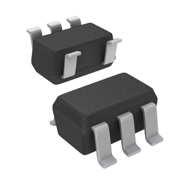
| 产品图片 |
|
| rohs | 符合RoHS无铅 / 符合限制有害物质指令(RoHS)规范要求 |
| 产品系列 | 电源管理 IC,低压差稳压器,Texas Instruments TPS79118DBVR- |
| 数据手册 | |
| 产品型号 | TPS79118DBVR |
| PCN设计/规格 | |
| 产品目录页面 | |
| 产品种类 | 低压差稳压器 |
| 供应商器件封装 | SOT-23-5 |
| 其它名称 | 296-11865-6 |
| 包装 | Digi-Reel® |
| 单位重量 | 13 mg |
| 商标 | Texas Instruments |
| 回动电压—最大值 | 57 mV |
| 安装类型 | 表面贴装 |
| 安装风格 | SMD/SMT |
| 封装 | Reel |
| 封装/外壳 | SC-74A,SOT-753 |
| 封装/箱体 | SOT-23-5 |
| 工作温度 | -40°C ~ 85°C |
| 工厂包装数量 | 3000 |
| 最大功率耗散 | 0.561 W |
| 最大工作温度 | + 85 C |
| 最大输入电压 | 5.5 V |
| 最小工作温度 | - 40 C |
| 最小输入电压 | + 2.7 V |
| 标准包装 | 1 |
| 电压-跌落(典型值) | - |
| 电压-输入 | 2.7 V ~ 5.5 V |
| 电压-输出 | 1.8V |
| 电压调节准确度 | 2 % |
| 电流-输出 | 100mA |
| 电流-限制(最小值) | 285mA |
| 稳压器拓扑 | 正,固定式 |
| 稳压器数 | 1 |
| 系列 | TPS79118 |
| 线路调整率 | 0.05 % / V |
| 负载调节 | 5 mV |
| 输入偏压电流—最大 | 0.17 mA |
| 输出电压 | 1.8 V |
| 输出电流 | 100 mA |
| 输出端数量 | 1 Output |
| 输出类型 | Fixed |
| 配用 | /product-detail/zh/TPS76918EVM-127/296-11034-ND/381776/product-detail/zh/TPS76901EVM-127/296-11030-ND/381854/product-detail/zh/TPS76XXXEVM-125/296-11042-ND/381857/product-detail/zh/TPS79301EVM/296-13593-ND/486551/product-detail/zh/TPS79328EVM/296-13594-ND/486552/product-detail/zh/DEM-SOT23LDO/296-20843-ND/1216448 |


- 商务部:美国ITC正式对集成电路等产品启动337调查
- 曝三星4nm工艺存在良率问题 高通将骁龙8 Gen1或转产台积电
- 太阳诱电将投资9.5亿元在常州建新厂生产MLCC 预计2023年完工
- 英特尔发布欧洲新工厂建设计划 深化IDM 2.0 战略
- 台积电先进制程称霸业界 有大客户加持明年业绩稳了
- 达到5530亿美元!SIA预计今年全球半导体销售额将创下新高
- 英特尔拟将自动驾驶子公司Mobileye上市 估值或超500亿美元
- 三星加码芯片和SET,合并消费电子和移动部门,撤换高东真等 CEO
- 三星电子宣布重大人事变动 还合并消费电子和移动部门
- 海关总署:前11个月进口集成电路产品价值2.52万亿元 增长14.8%


PDF Datasheet 数据手册内容提取
Product Order Technical Tools & Support & Folder Now Documents Software Community TPS791 SLVS325D–MARCH2001–REVISEDFEBRUARY2018 TPS791 Ultralow Noise, High PSRR, Fast RF 100-mA Low-Dropout Linear Regulators 1 Features 3 Description • 100-mALow-DropoutRegulatorWith EN The TPS791 device is a low-dropout (LDO) low- 1 power linear voltage regulator that features high • Availablein1.8-V,3.3-V,4.7-V,andAdj. power-supply rejection ratio (PSRR), ultralow noise, • HighPSRR(70dBat10kHz) fast start-up, and excellent line and load transient • UltralowNoise(15µV ) responses in a small outline, SOT23 package. The RMS device is stable, with a small 1-µF ceramic capacitor • FastStart-UpTime(63 µs) on the output. The TPS791 uses an advanced, • StableWithAny1-µFCeramicCapacitor proprietary BiCMOS fabrication process to yield • ExcellentLoad,LineTransient extremely low dropout voltages (for example, 38 mV at 100 mA, TPS79147). This device achieves fast • VeryLowDropoutVoltage(38mVatFullLoad, start-up times (approximately 63 µs with a 0.001-µF TPS79147) bypass capacitor) while consuming very low • 5-PinSOT23(DBV)Package quiescent current (170 µA typical). Moreover, when • TPS792xxProvidesENOptions the device is placed in standby mode, the supply current is reduced to less than 1 µA. The TPS79118 2 Applications exhibits approximately 15 µV of output voltage RMS noise with a 0.1-µF bypass capacitor. Applications • PoweringVCOsandPLLs with analog components that are noise sensitive, • BluetoothandWirelessLAN such as portable RF electronics, benefit from the high • PortableandBatteryOperated PSRR and low noise features as well as the fast responsetime. DeviceInformation(1) PARTNUMBER PACKAGE BODYSIZE(NOM) SOT23(5) 2.90mm×1.60mm TPS791 SOT23(6) 2.90mm×1.60mm (1) For all available packages, see the orderable addendum at theendofthedatasheet. SimplifiedSchematic:FixedOutput SimplifiedSchematic:AdjustableOutput VIN IN OUT VOUT VIN IN OUT VOUT 1 PF 1 PF 1 PF 100 pF R1 1 PF FB TPS791 TPS79101 R 2 EN BYPASS VEN EN BYPASS GND 0.1 PF VEN GND (cid:19)(cid:17)(cid:20)(cid:3)PF Copyright © 2018, Texas Instruments Incorporated Copyright © 2017, Texas Instruments Incorporated 1 An IMPORTANT NOTICE at the end of this data sheet addresses availability, warranty, changes, use in safety-critical applications, intellectualpropertymattersandotherimportantdisclaimers.PRODUCTIONDATA.
TPS791 SLVS325D–MARCH2001–REVISEDFEBRUARY2018 www.ti.com Table of Contents 1 Features.................................................................. 1 7.4 DeviceFunctionalModes........................................15 2 Applications........................................................... 1 8 ApplicationandImplementation........................ 16 3 Description............................................................. 1 8.1 ApplicationInformation............................................16 4 RevisionHistory..................................................... 2 8.2 TypicalApplication .................................................16 8.3 Do'sandDon'ts.......................................................17 5 PinConfigurationandFunctions......................... 3 9 PowerSupplyRecommendations...................... 18 6 Specifications......................................................... 3 10 Layout................................................................... 18 6.1 AbsoluteMaximumRatings......................................3 6.2 ESDRatings..............................................................4 10.1 LayoutGuidelines.................................................18 6.3 RecommendedOperatingConditions.......................4 10.2 LayoutExample....................................................18 6.4 ThermalInformation..................................................4 11 DeviceandDocumentationSupport................. 19 6.5 ElectricalCharacteristics...........................................5 11.1 ReceivingNotificationofDocumentationUpdates19 6.6 TypicalCharacteristics..............................................6 11.2 CommunityResources..........................................19 7 DetailedDescription............................................ 12 11.3 Trademarks...........................................................19 7.1 Overview.................................................................12 11.4 ElectrostaticDischargeCaution............................19 7.2 FunctionalBlockDiagrams.....................................12 11.5 Glossary................................................................19 7.3 FeatureDescription.................................................13 12 Mechanical,Packaging,andOrderable Information........................................................... 19 4 Revision History NOTE:Pagenumbersforpreviousrevisionsmaydifferfrompagenumbersinthecurrentversion. ChangesfromRevisionC(May2002)toRevisionD Page • AddedDeviceInformationtable,SimplifiedSchematicfigurestopage1,ESDRatingstable,ThermalInformation table,PinConfigurationandFunctionssection,Overviewsection,FeatureDescriptionsection,DeviceFunctional Modessection,ApplicationandImplementationsection,PowerSupplyRecommendationssection,Layoutsection, DeviceandDocumentationSupportsection,andMechanical,Packaging,andOrderableInformationsection...................1 • ChangedTPS791xxtoTPS791throughoutdocument ......................................................................................................... 1 • ChangedApplicationssection ............................................................................................................................................... 1 • ChangedDescriptionsection................................................................................................................................................. 1 • DeletedOrderingInformationtable........................................................................................................................................ 3 • ChangedENpindescription .................................................................................................................................................. 3 • AddedI/OdataforGNDpin .................................................................................................................................................. 3 • DeletedPackageDissipationRatingtable............................................................................................................................. 3 • ChangedV toV ,I toI ,C toC ,C andC toC throughoutdocument .............................................. 3 I IN O OUT O OUT o(byp) (byp) BYPASS • Changedformulainfootnote1ofRecommendedOperatingConditionstable...................................................................... 4 • AddedVREFparametertoElectricalCharacteristicstable.................................................................................................... 5 • ChangedV toV intestconditionsofUVLOthresholdandUVLOhysteresisparameters............................................... 5 CC IN • AddedPSRRandV symbolstoPower-supplyripplerejectionandDropoutvoltageparameters...................................... 5 DO • AddedconditionsstatementtoTypicalCharacteristicssection ............................................................................................ 6 • ChangedI toC inTPS79118OutputSpectralNoiseDensityvsFrequencyfigure................................................ 7 OUT BYPASS • ChangedI toC inTPS79133OutputSpectralNoiseDensityvsFrequencyfigure................................................ 7 OUT BYPASS • ChangedthirdbulletinNormalOperationsection............................................................................................................... 15 • ChangedfirstbulletinDisabledsection .............................................................................................................................. 15 • ChangedV columninDeviceFunctionalModeComparisontable................................................................................... 15 EN • Addedactive-lowtoApplicationInformationdescription ..................................................................................................... 16 2 SubmitDocumentationFeedback Copyright©2001–2018,TexasInstrumentsIncorporated ProductFolderLinks:TPS791
TPS791 www.ti.com SLVS325D–MARCH2001–REVISEDFEBRUARY2018 5 Pin Configuration and Functions DBVPackage:AdjustableOutput DBVPackage:FixedOutput 6-PinSOT23 5-PinSOT23 TopView TopView IN 1 6 OUT IN 1 5 OUT GND 2 5 FB GND 2 EN 3 4 BYPASS EN 3 4 BYPASS Not to scale Not to scale PinFunctions PIN I/O DESCRIPTION NAME ADJ FIXED Anexternalbypasscapacitorconnectedtothispin,inconjunctionwithaninternal BYPASS 4 4 — resistor,createsalow-passfiltertofurtherreduceregulatornoise. TheENpinisaninputwhichenablesorshutsdownthedevice.Theenablesignal isanactive-lowdigitalcontrolthatenablesthedevice,sowhenENisalogichigh EN 3 3 I (>2V),thedeviceisinshutdownmode.WhenENislogiclow(<0.7V),the deviceisenabled. FB 5 N/A I Thispinisthefeedbackinputvoltagefortheadjustabledevice. GND 2 2 — Regulatorground. IN 1 1 I TheINpinistheinputtothedevice. OUT 6 5 O TheOUTpinistheregulatedoutputofthedevice. 6 Specifications 6.1 Absolute Maximum Ratings overoperatingfree-airtemperaturerange(unlessotherwisenoted)(1) MIN MAX UNIT Inputvoltagerange(2) –0.3 6 V VoltagerangeatEN –0.3 V +0.3 V IN VoltageonOUT –0.3 6 V Peakoutputcurrent Internallylimited SeeThermalInformation Continuoustotalpowerdissipation table Operatingvirtualjunctiontemperature,T –40 150 °C J Operatingambienttemperature,T –40 85 °C A Storagetemperature,T –65 150 °C stg (1) StressesbeyondthoselistedunderAbsoluteMaximumRatingsmaycausepermanentdamagetothedevice.Thesearestressratings only,whichdonotimplyfunctionaloperationofthedeviceattheseoranyotherconditionsbeyondthoseindicatedunderRecommended OperatingConditions.Exposuretoabsolute-maximum-ratedconditionsforextendedperiodsmayaffectdevicereliability. (2) Allvoltagevaluesarewithrespecttothenetworkgroundpin. Copyright©2001–2018,TexasInstrumentsIncorporated SubmitDocumentationFeedback 3 ProductFolderLinks:TPS791
TPS791 SLVS325D–MARCH2001–REVISEDFEBRUARY2018 www.ti.com 6.2 ESD Ratings VALUE UNIT Human-bodymodel(HBM),perANSI/ESDA/JEDECJS-001(1) ±2000 V Electrostaticdischarge V (ESD) Charged-devicemodel(CDM),perJEDECspecificationJESD22-C101(2) ±500 (1) JEDECdocumentJEP155statesthat500-VHBMallowssafemanufacturingwithastandardESDcontrolprocess. (2) JEDECdocumentJEP157statesthat250-VCDMallowssafemanufacturingwithastandardESDcontrolprocess. 6.3 Recommended Operating Conditions overoperatingfree-airtemperaturerange(unlessotherwisenoted) MIN NOM MAX UNIT V Inputvoltage(1) 2.7 5.5 V IN I Continuousoutputcurrent(2) 0 100 mA OUT T Operatingjunctiontemperature –40 125 °C J (1) Tocalculatetheminimuminputvoltageforyourmaximumoutputcurrent,usethefollowingformula: V (min)=V (max)+dropoutvoltage(V )atmaximumload. IN OUT DO (2) Continuousoutputcurrentandoperatingjunctiontemperaturearelimitedbyinternalprotectioncircuitry,butthedeviceisnot recommendedtobeoperatedunderconditionsbeyondthosespecifiedinthistableforextendedperiodsoftime. 6.4 Thermal Information TPS791 THERMALMETRIC(1) DBV(SOT23) DBV(SOT23) UNIT 5PINS 6PINS R Junction-to-ambientthermalresistance 192.6 168.2 °C/W θJA R Junction-to-case(top)thermalresistance 104.2 87.1 °C/W θJC(top) R Junction-to-boardthermalresistance 55.2 36.9 °C/W θJB ψ Junction-to-topcharacterizationparameter 24.1 17.1 °C/W JT ψ Junction-to-boardcharacterizationparameter 54.8 36.6 °C/W JB R Junction-to-case(bottom)thermalresistance N/A N/A °C/W θJC(bot) (1) Formoreinformationabouttraditionalandnewthermalmetrics,seetheSemiconductorandICPackageThermalMetricsapplication report. 4 SubmitDocumentationFeedback Copyright©2001–2018,TexasInstrumentsIncorporated ProductFolderLinks:TPS791
TPS791 www.ti.com SLVS325D–MARCH2001–REVISEDFEBRUARY2018 6.5 Electrical Characteristics overrecommendedoperatingfree-airtemperaturerange,(T =–40°Cto125°C),V =V +1V,I =1mA,EN=0V, J IN OUT(typ) OUT C =10µF,C =0.01µF(unlessotherwisenoted) OUT BYPASS PARAMETER TESTCONDITIONS MIN TYP MAX UNIT T =25°C,1.22V≤V ≤5.2V V J OUT OUT TPS79101 0.98 1.02 0µA<IOUT<100mA(1),1.22V≤VOUT≤5.2V V V OUT OUT T =25°C 1.8 J TPS79118 Outputvoltage 0µA<IOUT<100mA,2.8V<VIN<5.5V 1.764 1.836 V T =25°C 3.3 J TPS79133 0µA<I <100mA,4.3V<V <5.5V 3.234 3.366 OUT IN T =25°C 4.7 J TPS79147 0µA<I <100mA,5.2V<V <5.5V 4.606 4.794 OUT IN VREF Referencevoltage 1.2246 V 0µA<I <100mA,T =25°C 170 OUT J Quiescentcurrent(GNDcurrent) µA 0µA<I <100mA 250 OUT Loadregulation 0µA<I <100mA,T =25°C 5 mV OUT J ΔVOUT/ Outputvoltagelineregulation(2) VOUT+1V<VIN≤5.5V,TJ=25°C 0.05 %/V VOUT VOUT+1V<VIN≤5.5V 0.12 C =0.001µF 32 BYPASS BW=100Hzto C =0.0047µF 17 BYPASS Outputnoisevoltage(TPS79118) 100kHz,I = µV OUT RMS 100mA,TJ=25°C CBYPASS=0.01µF 16 C =0.1µF 15 BYPASS C =0.001µF 53 BYPASS R =33Ω,C = Time,start-up(TPS79133) L OUT C =0.0047µF 67 µs 1µF,T =25°C BYPASS J C =0.01µF 98 BYPASS Outputcurrentlimit VOUT=0V(1) 285 600 mA UVLOthreshold V rising 2.25 2.65 V IN UVLOhysteresis T =25°C,V rising 100 mV J IN Standbycurrent EN=V ,2.7V<V <5.5V 0.07 1 µA IN IN Highlevelenableinputvoltage 2.7V<V <5.5V 2 V IN Lowlevelenableinputvoltage 2.7V<V <5.5V 0.7 V IN Inputcurrent(EN) EN=V –1 1 µA IN f=100Hz,T =25°C,I =10mA 80 J OUT f=100Hz,T =25°C,I =100mA 75 J OUT TPS79118 f=10kHz,T =25°C,I =100mA 72 J OUT Power-supplyripple f=100kHz,TJ=25°C,IOUT=100mA 45 PSRR dB rejection f=100Hz,T =25°C,I =10mA 70 J OUT f=100Hz,T =25°C,I =100mA 75 J OUT TPS79133 f=10kHz,T =25°C,I =100mA 73 J OUT f=100kHz,T =25°C,I =100mA 37 J OUT I =100mA,T =25°C 50 OUT J TPS79133 I =100mA 90 OUT VDO Dropoutvoltage(3) mV I =100mA,T =25°C 38 OUT J TPS79147 I =100mA 70 OUT (1) TheminimumV operatingvoltageis2.7VorV +1V,whicheverisgreater.ThemaximumV voltageis5.5V.Themaximum IN OUT(typ) IN outputcurrentis100mA. (2) IfV ≤1.8VthenV =2.7VandV =5.5V. OUT INmin INmax (3) EqualsV voltage–V (typ)–100mV;theTPS79118dropoutvoltageislimitedbytheminimuminputvoltagerangelimitations. IN OUT Copyright©2001–2018,TexasInstrumentsIncorporated SubmitDocumentationFeedback 5 ProductFolderLinks:TPS791
TPS791 SLVS325D–MARCH2001–REVISEDFEBRUARY2018 www.ti.com 6.6 Typical Characteristics atT =25°C,V =V +1V,I =1mA,EN=0V,C =10µF,andC =0.01µF(unlessotherwisenoted) J IN OUT(typ) OUT OUT BYPASS 1.803 3.303 1.802 3.302 V V – – Ooltautput Vge 1.810.18 Outpuoltaget V 3.330.13 – 1.799 – 3.299 UT UT O O V 1.798 V 3.298 1.797 3.297 0 20 40 60 80 100 0 20 40 60 80 100 IOUT–Output Current–mA IOUT–Output Current–mA VIN=2.8V,COUT=10µF,TJ=25°C VIN=4.3V,COUT=10µF,TJ=25°C Figure1.TPS79118OutputVoltagevsOutputCurrent Figure2.TPS79133OutputVoltagevsOutputCurrent 1.82 3.32 1.815 V V 3.31 – 1.81 – –oltOutput Vage 11..78190.558 IOUT=1mA –Output oltageV 3.32.93 IOUT=IO1U0T0=m1AmA UT IOUT=100mA UT O 1.79 O V V 3.28 1.785 1.78 3.27 –40–25–10 5 20 35 50 65 80 95 110125 –40–25–10 5 20 35 50 65 80 95 110125 TJ–Junction Temperature–°C TJ–Junction Temperature–°C VIN=2.8V,COUT=10µF VIN=4.3V,COUT=10µF Figure3.TPS79118OutputVoltagevs Figure4.TPS79133OutputVoltagevs JunctionTemperature JunctionTemperature 260 0.2 240 Hz 0.18 V/ 0.16 A 220 m m – 0.14 Ground Current– 111246800000 IOUT=1mAIOUT=100mA ctral Noise Density 000...0001.6821 IOUT=1IOmUAT=100mA pe 0.04 S 120 ut 0.02 p 100 Out 0 –40–25–10 5 20 35 50 65 80 95110125 100 1k 10k 100k TJ–Junction Temperature–°C f–Frequency–Hz V =4.3V,C =10µF V =2.8V,C =1µF,C =0.1µF IN OUT IN OUT BYPASS Figure5.TPS79133GroundCurrentvs Figure6.TPS79118OutputSpectralNoiseDensityvs JunctionTemperature Frequency 6 SubmitDocumentationFeedback Copyright©2001–2018,TexasInstrumentsIncorporated ProductFolderLinks:TPS791
TPS791 www.ti.com SLVS325D–MARCH2001–REVISEDFEBRUARY2018 Typical Characteristics (continued) atT =25°C,V =V +1V,I =1mA,EN=0V,C =10µF,andC =0.01µF(unlessotherwisenoted) J IN OUT(typ) OUT OUT BYPASS 0.25 1.2 Hz Hz CBYPASS=0.001mF mV/Output Spectral Noise Density– 00..0001..55120 IOUT=1IOmUTA=100mA mV/Output Spectral Noise Density– 0000....012468 CBCYBPYAPCSABSSY=SP=0A.S01S.0m=0F047.01mFmF 100 1k 10k 100k 100 1k 10k 100k f–Frequency–Hz f–Frequency–Hz VIN=2.8V,COUT=10µF,CBYPASS=0.1µF VIN=2.8V,IOUT=100mA,COUT=10µF Figure7.TPS79118OutputSpectralNoiseDensityvs Figure8.TPS79118OutputSpectralNoiseDensityvs Frequency Frequency 0.4 0.4 Hz 0.35 Hz 0.35 mV/ 0.3 mV/ 0.3 – – Density 0.02.52 IOUT=100mA Density 0.02.52 IOUT=100mA e e s s Noi 0.15 Noi 0.15 ctral 0.1 IOUT=1mA ctral 0.1 IOUT=1mA e e p p ut S 0.05 ut S 0.05 p p Out 0 Out 0 100 1k 10k 100k 100 1k 10k 100k f–Frequency–Hz f–Frequency–Hz V =4.3V,C =1µF,C =0.1µF V =4.3V,C =10µF,C =0.1µF IN OUT BYPASS IN OUT BYPASS Figure9.TPS79133OutputSpectralNoiseDensityvs Figure10.TPS79133OutputSpectralNoiseDensityvs Frequency Frequency 2 70 – Hz 1.8 CBYPASS=0.001mF oise 60 mV/ 1.6 ut N Spectral Noise Density– 00011.....468241 CCBBYYPPCAABSSYSSP==AS00S..10=0m40F7.01mFmF Root Mean Squared OutpmV(RMS) 23450000 VVOOUUTT==13..83VV Output 0.20 RMS– 100 100 1k 10k 100k 0.001 0.01 0.1 f–Frequency–Hz C(BYPASS)–BypassCapacitance–mF VIN=4.3V,IOUT=100mA,COUT=10µF BW=100Hzto100kHz Figure11.TPS79133OutputSpectralNoiseDensityvs Figure12.RootMeanSquaredOutputNoisevs Frequency BypassCapacitance Copyright©2001–2018,TexasInstrumentsIncorporated SubmitDocumentationFeedback 7 ProductFolderLinks:TPS791
TPS791 SLVS325D–MARCH2001–REVISEDFEBRUARY2018 www.ti.com Typical Characteristics (continued) atT =25°C,V =V +1V,I =1mA,EN=0V,C =10µF,andC =0.01µF(unlessotherwisenoted) J IN OUT(typ) OUT OUT BYPASS 3 80 70 W 2.5 V – m 60 e – pedanc 2 IOUT=1mA oltageV 50 IOUT=100mA Output Im 1.51 Dropout 3400 –o IOUT=100mA –O 20 Z 0.5 VD 10 IOUT=10mA 0 0 10 100 1k 10k 100k 1M 10M –40–25–10 5 20 35 50 65 80 95 110125 f–Frequency–Hz TJ–Junction Temperature–°C VIN=4.3V,COUT=10µF,TJ=25°C VIN=3.2V,COUT=10µF Figure13.TPS79133OutputImpedancevsFrequency Figure14.TPS79133DropoutVoltagevs JunctionTemperature 100 120 90 mV 80 mV 100 ge– 70 TJ=125°C ge– 80 TJ=125°C oltaut V 5600 TJ=25°C oltut Va 60 opo 40 opo TJ=25°C Dr Dr 40 –O 30 –O TJ=–40°C D 20 D V TJ=–40°C V 20 10 0 0 0 0.02 0.04 0.06 0.08 0.1 2.5 3 3.5 4 4.5 5 IOUT–Output Current–A VIN–Input Voltage–V V =3.2V,C =10µF I =100mA IN OUT OUT Figure15.TPS79133DropoutVoltagevsOutputCurrent Figure16.TPS79101DropoutVoltagevsInputVoltage 5.2 90 IOUT=1mA V 80 – 4.7 e g 70 olta 4.2 dB m Required Input V 33..27 TJ=–40°TCJ=125°CTJ=25°C Ripple Rejection– 34560000 IOUT=100mA u 20 m 2.7 Mini 10 2.2 0 1.5 2 2.5 3 3.5 4 4.5 5 100 1k 10k 100k 1M 10M VOUT–Output Voltage–V f–Frequency–Hz V =3.2V,C =10µF V =2.8V,C =10µF,C =0.01µF IN OUT IN OUT BYPASS Figure17.MinimumRequiredInputVoltagevs Figure18.TPS79118RippleRejectionvsFrequency OutputVoltage 8 SubmitDocumentationFeedback Copyright©2001–2018,TexasInstrumentsIncorporated ProductFolderLinks:TPS791
TPS791 www.ti.com SLVS325D–MARCH2001–REVISEDFEBRUARY2018 Typical Characteristics (continued) atT =25°C,V =V +1V,I =1mA,EN=0V,C =10µF,andC =0.01µF(unlessotherwisenoted) J IN OUT(typ) OUT OUT BYPASS 90 90 80 IOUT=10mA 80 IOUT=10mA 70 70 B B d d – 60 – 60 n n o o cti 50 cti 50 e e Rej 40 Rej 40 e e Rippl 30 IOUT=100mA Rippl 30 IOUT=100mA 20 20 10 10 0 0 100 1k 10k 100k 1M 10M 100 1k 10k 100k 1M 10M f–Frequency–Hz f–Frequency–Hz V =2.8V,C =1µF,C =0.01µF V =2.8V,C =1µF,C =0.1µF IN OUT BYPASS IN OUT BYPASS Figure19.TPS79118RippleRejectionvsFrequency Figure20.TPS79118RippleRejectionvsFrequency 100 100 90 90 dB 80 IOUT=100mA dB 80 IOUT=100mA Ripple Rejection– 65740000 IOUT=10mA Ripple Rejection– 65740000 IOUT=10mA 30 30 20 20 10 100 1k 10k 100k 1M 10M 10 100 1k 10k 100k 1M 10M f–Frequency–Hz f–Frequency–Hz V =4.3V,C =10µF,C =0.01µF V =4.3V,C =1µF,C =0.01µF IN OUT BYPASS IN OUT BYPASS Figure21.TPS79133RippleRejectionvsFrequency Figure22.TPS79133RippleRejectionvsFrequency 100 3 V – 90 e 2 g a dB 80 IOUT=100mA eVolt 1 ection– 6700 Enabl 0 CBYPASS=0.001mF ej R ple 50 IOUT=10mA –V 3 Rip 40 – age 2 CBYPASS=0.0047mF UTolt 30 VOut V 1 CBYPASS=0.01mF p 20 Out 0 10 100 1k 10k 100k 1M 10M 0 20 40 60 80100 120140 160180200 t–Time–ms f–Frequency–Hz V =4.3V,V =3.3V,I =100mA,C =1µF,T =25°C V =4.3V,C =1µF,C =0.1µF IN OUT OUT OUT J IN OUT BYPASS Figure24.TPS79133OutputVoltage,EnableVoltagevs Figure23.TPS79133RippleRejectionvsFrequency Time(Start-Up) Copyright©2001–2018,TexasInstrumentsIncorporated SubmitDocumentationFeedback 9 ProductFolderLinks:TPS791
TPS791 SLVS325D–MARCH2001–REVISEDFEBRUARY2018 www.ti.com Typical Characteristics (continued) atT =25°C,V =V +1V,I =1mA,EN=0V,C =10µF,andC =0.01µF(unlessotherwisenoted) J IN OUT(typ) OUT OUT BYPASS V–OUTOutput Voltage–mV–11000 –Change InDVOUTOolutput Vtage–mV––2420000 V A – m e – V–INInput Voltag 32..88 Current Load1000 0 10 20 30 40 50 60 70 80 90 100 0 200400600800 1k 12k14k16k18k20k t–Time–ms t–Time–ms I =100mA,C =1µF,C =0.01µF V =2.8V,C =10µF OUT OUT BYPASS IN OUT Figure25.TPS79118LineTransientResponse Figure26.TPS79118LoadTransitResponse n V V–OUTut Voltage–mV–22000 –Change IOUTputoltage V–m –22000 utp DV Out O –40 A V 5.3 m 100 V–INnput Voltage– 4.3 I–OUTutput Current– 0 I 0 5 10 15 20 25 30 35 40 45 50 O 0 50 100150200250300350400450500 t–Time–ms t–Time–ms IOUT=100mA,COUT=1µF,CBYPASS=0.01µF, VIN=4.3V,COUT=10µF dv/dt=0.4V/m s Figure27.TPS79133LineTransientResponse Figure28.TPS79133LoadTransitResponse 100 100 W W – – e e c c an 10 an 10 sist RegionofInstability sist RegionofInstability e e R R s s erie 1 erie 1 S S nt nt e e al al uiv 0.1 uiv 0.1 Eq Eq RegionofStability – Regionof – R Instability R ES 0.01 ES 0.01 0 0.02 0.04 0.06 0.08 0.1 0 0.02 0.04 0.06 0.08 0.1 IOUT–Output Current–A IOUT–Output Current–A V =5.5V,C =0.47µF,T =–40°Cto125°C V =5.5V,C =1µF,T =–40°Cto125°C IN OUT J IN OUT J Figure29.TPS79118TypicalRegionsofStabilityEquivalent Figure30.TPS79118TypicalRegionsofStabilityEquivalent SeriesResistance(ESR)vsOutputCurrent SeriesResistance(ESR)vsOutputCurrent 10 SubmitDocumentationFeedback Copyright©2001–2018,TexasInstrumentsIncorporated ProductFolderLinks:TPS791
TPS791 www.ti.com SLVS325D–MARCH2001–REVISEDFEBRUARY2018 Typical Characteristics (continued) atT =25°C,V =V +1V,I =1mA,EN=0V,C =10µF,andC =0.01µF(unlessotherwisenoted) J IN OUT(typ) OUT OUT BYPASS 100 W – e c an 10 sist RegionofInstability e R s e eri 1 S nt e al v 0.1 qui RegionofStability E – R ES 0.01 0 0.02 0.04 0.06 0.08 0.1 IOUT–Output Current–A V =5.5V,C =10µF,T =–40°Cto125°C IN OUT J Figure31.TPS79118TypicalRegionsofStabilityEquivalent SeriesResistance(ESR)vsOutputCurrent Copyright©2001–2018,TexasInstrumentsIncorporated SubmitDocumentationFeedback 11 ProductFolderLinks:TPS791
TPS791 SLVS325D–MARCH2001–REVISEDFEBRUARY2018 www.ti.com 7 Detailed Description 7.1 Overview The TPS791 device is a high PSRR, ultra-low noise, 100-mA linear regulator (LDO). The fast start-up time and the excellent load and line transient behavior of this device qualify the TPS791 to be an ideal solution for signal RFandsignal-chainapplications. 7.2 Functional Block Diagrams V V IN OUT UVLO Current Sense SHUTDOWN ILIM R1 GND _ + FB EN R2 UVLO Thermal Shutdown External to the Device Bandgap 250 kW V Bypass IN Reference Copyright © 2018,Texas Instruments Incorporated Figure32. FunctionalBlockDiagram:AdjustableVersion V V IN OUT UVLO Current Sense GND SHUTDOWN ILIM R1 _ + EN UVLO R2 Thermal Shutdown Bandgap 250 kW VREF V Bypass IN Reference Copyright © 2018,Texas Instruments Incorporated Figure33. FunctionalBlockDiagram:FixedVersion 12 SubmitDocumentationFeedback Copyright©2001–2018,TexasInstrumentsIncorporated ProductFolderLinks:TPS791
TPS791 www.ti.com SLVS325D–MARCH2001–REVISEDFEBRUARY2018 7.3 Feature Description 7.3.1 PowerDissipationandJunctionTemperature Specified regulator operation is confirmed at a junction temperature of 125°C; restrict the maximum junction temperature to 125°C under normal operating conditions. This restriction limits the power dissipation the regulator can handle in any given application. To ensure the junction temperature is within acceptable limits, calculate the maximum allowable dissipation, P , and the actual dissipation, P , which must be less than or D(max) D equaltoP . D(max) Themaximum-power-dissipationlimitisdeterminedusingthefollowingequation: T max (cid:16)T P (cid:11)max(cid:12) J A D R TJA where • Tmaxisthemaximumallowablejunctiontemperature J • R isthethermalresistancejunction-to-ambientforthepackage(seetheThermalInformationtable) θJA • T istheambienttemperature (1) A Theregulatordissipationiscalculatedusing: P =(V –V )×I (2) D IN OUT OUT Power dissipation resulting from quiescent current is negligible. Excessive power dissipation triggers the thermal protectioncircuit. 7.3.2 ProgrammingtheTPS79101AdjustableRegulator The output voltage of the TPS79101 adjustable regulator is programmed using an external resistor divider; see Figure32.Theoutputvoltageiscalculatedusing: § R1• V VREFu¤1(cid:14) ‚ OUT ' R2„ where • VREF=1.2246Vtyp(theinternalreferencevoltage) (3) Select resistors R1 and R2 for approximately a 50-µA divider current. Lower value resistors can be used for improved noise performance, but the solution consumes more power. Avoid higher resistor values because leakage current into or out of FB across R1, R2 creates an offset voltage that artificially increases or decreases the feedback voltage and thus erroneously decreases or increases V . The recommended design procedure is OUT tochooseR2=30.1kΩ tosetthedividercurrentat50 µA,C1=15pFforstability,andthencalculateR1using: § V • R1 ¤ OUT (cid:16)1‚uR2 'VREF „ (4) In order to improve the stability of the adjustable version, a small compensation capacitor is suggested to be placed between OUT and FB. For voltages < 1.8 V, the value of this capacitor must be 100 pF. For voltages > 1.8V,theapproximatevalueofthiscapacitorcanbecalculatedas: (cid:11)3u10(cid:16)7(cid:12)u(cid:11)R1(cid:14)R2(cid:12) C1 (cid:11)R1uR2(cid:12) (5) Copyright©2001–2018,TexasInstrumentsIncorporated SubmitDocumentationFeedback 13 ProductFolderLinks:TPS791
TPS791 SLVS325D–MARCH2001–REVISEDFEBRUARY2018 www.ti.com Feature Description (continued) The table in Figure 34 shows the suggested value of this capacitor for several resistor ratios. If this capacitor is not used (such as in a unity-gain configuration) or if an output voltage < 1.8 V is chosen, then the minimum recommendedoutputcapacitoris2.2 µFinsteadof1 µF. TPS79101 OUTPUT VOLTAGE VI IN PROGRAMMING GUIDE 1 µF OUTPUT R1 R2 C1 VOLTAGE ≥ 2 V EN OUT C1 VO 2.5 V 31.6 kΩ 30.1 kΩ 22 pF R1 ≤ 0.7 V 1 µF 3.3 V 51 kΩ 30.1 kΩ 15 pF BYPASS FB 3.6 V 59 kΩ 30.1 kΩ 15 pF 0.01 µF GND R2 Figure34. TPS79101AdjustableLDORegulatorProgramming 7.3.3 RegulatorProtection The TPS791 PMOS-pass transistor has a built-in back diode that conducts reverse current when the input voltage drops below the output voltage (for example, during power-down). Current is conducted from the output to the input and is not internally limited. If extended reverse voltage operation is anticipated, external limiting may beappropriate. The TPS791 features internal current limiting and thermal protection. During normal operation, the TPS791 limits output current to approximately 400 mA. When current limiting engages, the output voltage scales back linearly until the overcurrent condition ends. Although current limiting is designed to prevent gross device failure, care must be taken not to exceed the power dissipation ratings of the package or the absolute maximum voltage ratings of the device. If the temperature of the device exceeds approximately 165°C, thermal-protection circuitry shuts the device down. When the device cools down to below approximately 140°C, regulator operation resumes. 14 SubmitDocumentationFeedback Copyright©2001–2018,TexasInstrumentsIncorporated ProductFolderLinks:TPS791
TPS791 www.ti.com SLVS325D–MARCH2001–REVISEDFEBRUARY2018 7.4 Device Functional Modes 7.4.1 NormalOperation Thedeviceregulatestothenominaloutputvoltageunderthefollowingconditions: • Theinputvoltageisatleastashighasthe|V | IN(min) • The input voltage magnitude is greater than the nominal output voltage magnitude added to the dropout voltage • |V |<low-levelenablepininputvoltage(0.7V) EN • Theoutputcurrentislessthanthecurrentlimit • Thedevicejunctiontemperatureislessthanthemaximumspecifiedjunctiontemperature 7.4.2 DropoutOperation If the input voltage magnitude is lower than the nominal output voltage magnitude plus the specified dropout voltage magnitude, but all other conditions are met for normal operation, the device operates in dropout mode. In this mode of operation, the output voltage magnitude is the same as the input voltage magnitude minus the dropout voltage magnitude. The transient performance of the device is significantly degraded because the pass device (such as a bipolar junction transistor, or BJT) is in saturation and no longer controls the current through theLDO.Lineorloadtransientsindropoutcanresultinlargeoutputvoltagedeviations. 7.4.3 Disabled Thedeviceisdisabledunderthefollowingconditions: • |V |>high-levelenablepininputvoltage(2V) EN • Thedevicejunctiontemperatureisgreaterthanthethermalshutdowntemperature Table1showstheconditionsthatleadtothedifferentmodesofoperation. Table1.DeviceFunctionalModeComparison PARAMETER OPERATINGMODE V V I T IN EN OUT J Normalmode |V |>{|V |+|V |,|V |} |V |<0.7V I <I T <125°C IN OUT(nom) DO IN(min) EN OUT CL J Dropoutmode |V |<|V |<|V |+|V | |V |<0.7V — T <125°C IN(min) IN OUT(nom) DO EN J Disabledmode — |V |>2V — T >170°C (anytrueconditiondisablesthedevice) EN J Copyright©2001–2018,TexasInstrumentsIncorporated SubmitDocumentationFeedback 15 ProductFolderLinks:TPS791
TPS791 SLVS325D–MARCH2001–REVISEDFEBRUARY2018 www.ti.com 8 Application and Implementation NOTE Information in the following applications sections is not part of the TI component specification, and TI does not warrant its accuracy or completeness. TI’s customers are responsible for determining suitability of components for their purposes. Customers should validateandtesttheirdesignimplementationtoconfirmsystemfunctionality. 8.1 Application Information TheTPS791low-dropout(LDO)regulatorisoptimizedforuseinnoise-sensitivebattery-operatedequipment.The device features extremely low dropout voltages, high PSRR, ultralow output noise, low quiescent current (170 µA typically), and an active-low, enable input to reduce supply currents to less than 1 µA when the regulator is turnedoff. 8.1.1 ExternalCapacitorRequirements A 0.1-µF or larger ceramic input bypass capacitor, connected between IN and GND and located close to the TPS791,isrequiredforstabilityandtoimprovetransientresponse,noiserejection,andripplerejection.Ahigher- value electrolytic input capacitor may be necessary if large, fast-rise-time load transients are anticipated and the deviceislocatedseveralinchesfromthepowersource. Like all low dropout regulators, the TPS791 requires an output capacitor connected between OUT and GND to stabilize the internal control loop. The minimum recommended capacitance is 1 µF. Any 1-µF or larger ceramic capacitorissuitable.Thedeviceisalsostablewitha0.47-µFceramiccapacitorwithatleast75mΩ ofESR. The internal voltage reference is a key source of noise in an LDO regulator. The TPS791 has a BYPASS pin that is connected to the voltage reference through a 250-kΩ internal resistor. The 250-kΩ internal resistor, in conjunction with an external bypass capacitor connected to the BYPASS pin, creates a low-pass filter to reduce the voltage reference noise and, therefore, the noise at the regulator output. In order for the regulator to operate properly, the current flow out of the BYPASS pin must be at a minimum because any leakage current creates an IR drop across the internal resistor thus creating an output error. Therefore, the bypass capacitor must have minimalleakagecurrent. For example, the TPS79118 exhibits approximately 15 µV of output voltage noise using a 0.1-µF ceramic RMS bypass capacitor and a 1-µF ceramic output capacitor. The output starts up slower as the bypass capacitance increases because of the RC time constant at the bypass pin that is created by the internal 250-kΩ resistor and externalcapacitor. 8.2 Typical Application Figure35showsatypicalapplicationcircuit. IN OUT VOUT 0.1 PF 1 PF TPS791 EN BYPASS GND 0.1(cid:3)PF Copyright © 2018, Texas Instruments Incorporated Figure35. TypicalApplicationCircuit 16 SubmitDocumentationFeedback Copyright©2001–2018,TexasInstrumentsIncorporated ProductFolderLinks:TPS791
TPS791 www.ti.com SLVS325D–MARCH2001–REVISEDFEBRUARY2018 Typical Application (continued) 8.2.1 DesignRequirements Table2showstheparametersusedforthisdesignexample. Table2.DesignParameters PARAMETER DESIGNREQUIREMENT Inputvoltage 4.3Vto3.5V(LithiumIonbattery) Outputvoltage 3.3V DCoutputcurrent 10mA Peakoutputcurrent 100mA Maximumambienttemperature 60°C 8.2.2 DetailedDesignProcedure Selectthedesiredoutputvoltageoption.Aninputcapacitorof0.1 µFisusedbecausethebatteryisconnectedto the input through a via and a short 10-mil (0.01-in) trace. An output capacitor of 1 mF is used in this design example. A smaller size output capacitor can be used up to a minimum of 1 µF to stabilize the internal control loop. 8.2.3 ApplicationCurves 100 3 V – 90 e 2 g a dB 80 IOUT=100mA eVolt 1 ection– 6700 Enabl 0 CBYPASS=0.001mF ej R ple 50 IOUT=10mA –V 3 Rip 40 – age 2 CBYPASS=0.0047mF UTolt 30 VOut V 1 CBYPASS=0.01mF p 20 Out 0 10 100 1k 10k 100k 1M 10M 0 20 40 60 80100 120140 160180200 t–Time–ms f–Frequency–Hz Figure37.TPS79133OutputVoltage,EnableVoltagevs Figure36.TPS79133RippleRejectionvsFrequency Time(Start-Up) 8.3 Do's and Don'ts Do place at least one, low-ESR, 1-µF capacitor as close as possible between the OUT pin of the regulator and theGNDpin. Do place at least one, low-ESR, 0.1-µF capacitor as close as possible between the IN pin of the regulator and theGNDpin. Doprovideadequatethermalpathsawayfromthedevice. Donotplacetheinputoroutputcapacitormorethan10mmawayfromtheregulator. Donotexceedtheabsolutemaximumratings. DonotfloattheEnable(EN)pin. DonotresistivelyorinductivelyloadtheBYPASSpin. Donotlettheoutputvoltagegetmorethan0.3Vabovetheinputvoltage. Copyright©2001–2018,TexasInstrumentsIncorporated SubmitDocumentationFeedback 17 ProductFolderLinks:TPS791
TPS791 SLVS325D–MARCH2001–REVISEDFEBRUARY2018 www.ti.com 9 Power Supply Recommendations This device is designed to operate from an input voltage supply range from 2.7 V to 5.5 V. The input voltage range must provide adequate headroom in order for the device to have a regulated output. This input supply must be well-regulated and stable. A 0.1-µF input capacitor is required for stability; if the input supply is noisy, additionalinputcapacitorswithlowESRcanhelpimprovetheoutputnoiseperformance. 10 Layout 10.1 Layout Guidelines Layout is a critical part of good power-supply design. There are several signal paths that conduct fast-changing currents or voltages that can interact with stray inductance or parasitic capacitance to generate noise or degrade the power-supply performance. To help eliminate these problems, bypass the IN pin to ground with a low ESR ceramicbypasscapacitorwithanX5RorX7Rdielectric. Equivalent series inductance (ESL) and equivalent series resistance (ESR) must be minimized to maximize performance and ensure stability. Every capacitor (C , C , C , and C ) must be placed as close as IN OUT BYPASS 1 possibletothedeviceandonthesamesideofthePCBastheregulatoritself. Do not place any capacitors on the opposite side of the PCB from where the regulator is installed. The use of vias and long traces is strongly discouraged because these circuits can impact system performance negatively, andevencauseinstability. 10.1.1 BoardLayoutRecommendationtoImprovePSRRandNoisePerformance To improve ac measurements such as PSRR, output noise, and transient response, TI recommends that the board be designed with separate ground planes for V and V , with each ground plane connected only at the IN OUT ground pin of the device. In addition, connect the ground connection for the bypass capacitor directly to the groundpinofthedevice. 10.2 Layout Example Output Ground Output Plane Input Plane IN OUT GND FB EN(1) BYPASS Input Ground NR and FB Ground Denotes via (1) TheENpinisactivelow. Figure38. LayoutExample(6-PinDBVPackage) 18 SubmitDocumentationFeedback Copyright©2001–2018,TexasInstrumentsIncorporated ProductFolderLinks:TPS791
TPS791 www.ti.com SLVS325D–MARCH2001–REVISEDFEBRUARY2018 11 Device and Documentation Support 11.1 Receiving Notification of Documentation Updates To receive notification of documentation updates, navigate to the device product folder on ti.com. In the upper right corner, click on Alert me to register and receive a weekly digest of any product information that has changed.Forchangedetails,reviewtherevisionhistoryincludedinanyreviseddocument. 11.2 Community Resources The following links connect to TI community resources. Linked contents are provided "AS IS" by the respective contributors. They do not constitute TI specifications and do not necessarily reflect TI's views; see TI's Terms of Use. TIE2E™OnlineCommunity TI'sEngineer-to-Engineer(E2E)Community.Createdtofostercollaboration amongengineers.Ate2e.ti.com,youcanaskquestions,shareknowledge,exploreideasandhelp solveproblemswithfellowengineers. DesignSupport TI'sDesignSupport QuicklyfindhelpfulE2Eforumsalongwithdesignsupporttoolsand contactinformationfortechnicalsupport. 11.3 Trademarks E2EisatrademarkofTexasInstruments. Allothertrademarksarethepropertyoftheirrespectiveowners. 11.4 Electrostatic Discharge Caution This integrated circuit can be damaged by ESD. Texas Instruments recommends that all integrated circuits be handled with appropriateprecautions.Failuretoobserveproperhandlingandinstallationprocedurescancausedamage. ESDdamagecanrangefromsubtleperformancedegradationtocompletedevicefailure.Precisionintegratedcircuitsmaybemore susceptibletodamagebecauseverysmallparametricchangescouldcausethedevicenottomeetitspublishedspecifications. 11.5 Glossary SLYZ022—TIGlossary. Thisglossarylistsandexplainsterms,acronyms,anddefinitions. 12 Mechanical, Packaging, and Orderable Information The following pages include mechanical, packaging, and orderable information. This information is the most current data available for the designated devices. This data is subject to change without notice and revision of thisdocument.Forbrowser-basedversionsofthisdatasheet,refertotheleft-handnavigation. Copyright©2001–2018,TexasInstrumentsIncorporated SubmitDocumentationFeedback 19 ProductFolderLinks:TPS791
PACKAGE OPTION ADDENDUM www.ti.com 6-Feb-2020 PACKAGING INFORMATION Orderable Device Status Package Type Package Pins Package Eco Plan Lead/Ball Finish MSL Peak Temp Op Temp (°C) Device Marking Samples (1) Drawing Qty (2) (6) (3) (4/5) TPS79101DBVR ACTIVE SOT-23 DBV 6 3000 Green (RoHS NIPDAU Level-1-260C-UNLIM -40 to 125 PEUI & no Sb/Br) TPS79101DBVRG4 ACTIVE SOT-23 DBV 6 3000 Green (RoHS NIPDAU Level-1-260C-UNLIM -40 to 125 PEUI & no Sb/Br) TPS79101DBVT ACTIVE SOT-23 DBV 6 250 Green (RoHS NIPDAU Level-1-260C-UNLIM -40 to 125 PEUI & no Sb/Br) TPS79118DBVR ACTIVE SOT-23 DBV 5 3000 Green (RoHS NIPDAU Level-1-260C-UNLIM -40 to 125 PERI & no Sb/Br) TPS79118DBVT ACTIVE SOT-23 DBV 5 250 Green (RoHS NIPDAU Level-1-260C-UNLIM -40 to 125 PERI & no Sb/Br) TPS79118DBVTG4 ACTIVE SOT-23 DBV 5 250 Green (RoHS NIPDAU Level-1-260C-UNLIM -40 to 125 PERI & no Sb/Br) TPS79133DBVR ACTIVE SOT-23 DBV 5 3000 Green (RoHS NIPDAU Level-1-260C-UNLIM -40 to 125 PESI & no Sb/Br) TPS79133DBVRG4 ACTIVE SOT-23 DBV 5 3000 Green (RoHS NIPDAU Level-1-260C-UNLIM -40 to 125 PESI & no Sb/Br) TPS79133DBVT ACTIVE SOT-23 DBV 5 250 Green (RoHS NIPDAU Level-1-260C-UNLIM -40 to 125 PESI & no Sb/Br) TPS79147DBVR ACTIVE SOT-23 DBV 5 3000 Green (RoHS NIPDAU Level-1-260C-UNLIM -40 to 125 PETI & no Sb/Br) TPS79147DBVT ACTIVE SOT-23 DBV 5 250 Green (RoHS NIPDAU Level-1-260C-UNLIM -40 to 125 PETI & no Sb/Br) TPS79147DBVTG4 ACTIVE SOT-23 DBV 5 250 Green (RoHS NIPDAU Level-1-260C-UNLIM -40 to 125 PETI & no Sb/Br) (1) The marketing status values are defined as follows: ACTIVE: Product device recommended for new designs. LIFEBUY: TI has announced that the device will be discontinued, and a lifetime-buy period is in effect. NRND: Not recommended for new designs. Device is in production to support existing customers, but TI does not recommend using this part in a new design. PREVIEW: Device has been announced but is not in production. Samples may or may not be available. OBSOLETE: TI has discontinued the production of the device. (2) RoHS: TI defines "RoHS" to mean semiconductor products that are compliant with the current EU RoHS requirements for all 10 RoHS substances, including the requirement that RoHS substance do not exceed 0.1% by weight in homogeneous materials. Where designed to be soldered at high temperatures, "RoHS" products are suitable for use in specified lead-free processes. TI may reference these types of products as "Pb-Free". RoHS Exempt: TI defines "RoHS Exempt" to mean products that contain lead but are compliant with EU RoHS pursuant to a specific EU RoHS exemption. Addendum-Page 1
PACKAGE OPTION ADDENDUM www.ti.com 6-Feb-2020 Green: TI defines "Green" to mean the content of Chlorine (Cl) and Bromine (Br) based flame retardants meet JS709B low halogen requirements of <=1000ppm threshold. Antimony trioxide based flame retardants must also meet the <=1000ppm threshold requirement. (3) MSL, Peak Temp. - The Moisture Sensitivity Level rating according to the JEDEC industry standard classifications, and peak solder temperature. (4) There may be additional marking, which relates to the logo, the lot trace code information, or the environmental category on the device. (5) Multiple Device Markings will be inside parentheses. Only one Device Marking contained in parentheses and separated by a "~" will appear on a device. If a line is indented then it is a continuation of the previous line and the two combined represent the entire Device Marking for that device. (6) Lead/Ball Finish - Orderable Devices may have multiple material finish options. Finish options are separated by a vertical ruled line. Lead/Ball Finish values may wrap to two lines if the finish value exceeds the maximum column width. Important Information and Disclaimer:The information provided on this page represents TI's knowledge and belief as of the date that it is provided. TI bases its knowledge and belief on information provided by third parties, and makes no representation or warranty as to the accuracy of such information. Efforts are underway to better integrate information from third parties. TI has taken and continues to take reasonable steps to provide representative and accurate information but may not have conducted destructive testing or chemical analysis on incoming materials and chemicals. TI and TI suppliers consider certain information to be proprietary, and thus CAS numbers and other limited information may not be available for release. In no event shall TI's liability arising out of such information exceed the total purchase price of the TI part(s) at issue in this document sold by TI to Customer on an annual basis. OTHER QUALIFIED VERSIONS OF TPS791 : •Automotive: TPS791-Q1 NOTE: Qualified Version Definitions: •Automotive - Q100 devices qualified for high-reliability automotive applications targeting zero defects Addendum-Page 2
PACKAGE MATERIALS INFORMATION www.ti.com 24-Apr-2020 TAPE AND REEL INFORMATION *Alldimensionsarenominal Device Package Package Pins SPQ Reel Reel A0 B0 K0 P1 W Pin1 Type Drawing Diameter Width (mm) (mm) (mm) (mm) (mm) Quadrant (mm) W1(mm) TPS79101DBVR SOT-23 DBV 6 3000 178.0 9.0 3.23 3.17 1.37 4.0 8.0 Q3 TPS79101DBVT SOT-23 DBV 6 250 178.0 9.0 3.23 3.17 1.37 4.0 8.0 Q3 TPS79118DBVR SOT-23 DBV 5 3000 178.0 9.0 3.23 3.17 1.37 4.0 8.0 Q3 TPS79118DBVT SOT-23 DBV 5 250 178.0 9.0 3.23 3.17 1.37 4.0 8.0 Q3 TPS79133DBVR SOT-23 DBV 5 3000 178.0 9.0 3.23 3.17 1.37 4.0 8.0 Q3 TPS79133DBVT SOT-23 DBV 5 250 178.0 9.0 3.23 3.17 1.37 4.0 8.0 Q3 TPS79147DBVR SOT-23 DBV 5 3000 178.0 9.0 3.3 3.2 1.4 4.0 8.0 Q3 TPS79147DBVT SOT-23 DBV 5 250 178.0 9.0 3.23 3.17 1.37 4.0 8.0 Q3 PackMaterials-Page1
PACKAGE MATERIALS INFORMATION www.ti.com 24-Apr-2020 *Alldimensionsarenominal Device PackageType PackageDrawing Pins SPQ Length(mm) Width(mm) Height(mm) TPS79101DBVR SOT-23 DBV 6 3000 180.0 180.0 18.0 TPS79101DBVT SOT-23 DBV 6 250 180.0 180.0 18.0 TPS79118DBVR SOT-23 DBV 5 3000 180.0 180.0 18.0 TPS79118DBVT SOT-23 DBV 5 250 180.0 180.0 18.0 TPS79133DBVR SOT-23 DBV 5 3000 180.0 180.0 18.0 TPS79133DBVT SOT-23 DBV 5 250 180.0 180.0 18.0 TPS79147DBVR SOT-23 DBV 5 3000 180.0 180.0 18.0 TPS79147DBVT SOT-23 DBV 5 250 180.0 180.0 18.0 PackMaterials-Page2
PACKAGE OUTLINE DBV0005A SOT-23 - 1.45 mm max height SCALE 4.000 SMALL OUTLINE TRANSISTOR C 3.0 2.6 0.1 C 1.75 1.45 1.45 B A 0.90 PIN 1 INDEX AREA 1 5 2X 0.95 3.05 2.75 1.9 1.9 2 4 3 0.5 5X 0.3 0.15 0.2 C A B (1.1) TYP 0.00 0.25 GAGE PLANE 0.22 TYP 0.08 8 TYP 0.6 0 0.3 TYP SEATING PLANE 4214839/E 09/2019 NOTES: 1. All linear dimensions are in millimeters. Any dimensions in parenthesis are for reference only. Dimensioning and tolerancing per ASME Y14.5M. 2. This drawing is subject to change without notice. 3. Refernce JEDEC MO-178. 4. Body dimensions do not include mold flash, protrusions, or gate burrs. Mold flash, protrusions, or gate burrs shall not exceed 0.15 mm per side. www.ti.com
EXAMPLE BOARD LAYOUT DBV0005A SOT-23 - 1.45 mm max height SMALL OUTLINE TRANSISTOR PKG 5X (1.1) 1 5 5X (0.6) SYMM (1.9) 2 2X (0.95) 3 4 (R0.05) TYP (2.6) LAND PATTERN EXAMPLE EXPOSED METAL SHOWN SCALE:15X SOLDER MASK SOLDER MASK METAL UNDER METAL OPENING OPENING SOLDER MASK EXPOSED METAL EXPOSED METAL 0.07 MAX 0.07 MIN ARROUND ARROUND NON SOLDER MASK SOLDER MASK DEFINED DEFINED (PREFERRED) SOLDER MASK DETAILS 4214839/E 09/2019 NOTES: (continued) 5. Publication IPC-7351 may have alternate designs. 6. Solder mask tolerances between and around signal pads can vary based on board fabrication site. www.ti.com
EXAMPLE STENCIL DESIGN DBV0005A SOT-23 - 1.45 mm max height SMALL OUTLINE TRANSISTOR PKG 5X (1.1) 1 5 5X (0.6) SYMM 2 (1.9) 2X(0.95) 3 4 (R0.05) TYP (2.6) SOLDER PASTE EXAMPLE BASED ON 0.125 mm THICK STENCIL SCALE:15X 4214839/E 09/2019 NOTES: (continued) 7. Laser cutting apertures with trapezoidal walls and rounded corners may offer better paste release. IPC-7525 may have alternate design recommendations. 8. Board assembly site may have different recommendations for stencil design. www.ti.com
PACKAGE OUTLINE DBV0006A SOT-23 - 1.45 mm max height SCALE 4.000 SMALL OUTLINE TRANSISTOR C 3.0 2.6 0.1 C 1.75 1.45 B A 1.45 MAX PIN 1 INDEX AREA 1 6 2X 0.95 3.05 2.75 1.9 5 2 4 3 0.50 6X 0.25 0.15 0.2 C A B (1.1) TYP 0.00 0.25 GAGE PLANE 0.22 TYP 0.08 8 TYP 0.6 0 0.3 TYP SEATING PLANE 4214840/B 03/2018 NOTES: 1. All linear dimensions are in millimeters. Any dimensions in parenthesis are for reference only. Dimensioning and tolerancing per ASME Y14.5M. 2. This drawing is subject to change without notice. 3. Body dimensions do not include mold flash or protrusion. Mold flash and protrusion shall not exceed 0.15 per side. 4. Leads 1,2,3 may be wider than leads 4,5,6 for package orientation. 5. Refernce JEDEC MO-178. www.ti.com
EXAMPLE BOARD LAYOUT DBV0006A SOT-23 - 1.45 mm max height SMALL OUTLINE TRANSISTOR PKG 6X (1.1) 1 6X (0.6) 6 SYMM 2 5 2X (0.95) 3 4 (R0.05) TYP (2.6) LAND PATTERN EXAMPLE EXPOSED METAL SHOWN SCALE:15X SOLDER MASK SOLDER MASK METAL UNDER METAL OPENING OPENING SOLDER MASK EXPOSED METAL EXPOSED METAL 0.07 MAX 0.07 MIN ARROUND ARROUND NON SOLDER MASK SOLDER MASK DEFINED DEFINED (PREFERRED) SOLDER MASK DETAILS 4214840/B 03/2018 NOTES: (continued) 6. Publication IPC-7351 may have alternate designs. 7. Solder mask tolerances between and around signal pads can vary based on board fabrication site. www.ti.com
EXAMPLE STENCIL DESIGN DBV0006A SOT-23 - 1.45 mm max height SMALL OUTLINE TRANSISTOR PKG 6X (1.1) 1 6X (0.6) 6 SYMM 2 5 2X(0.95) 3 4 (R0.05) TYP (2.6) SOLDER PASTE EXAMPLE BASED ON 0.125 mm THICK STENCIL SCALE:15X 4214840/B 03/2018 NOTES: (continued) 8. Laser cutting apertures with trapezoidal walls and rounded corners may offer better paste release. IPC-7525 may have alternate design recommendations. 9. Board assembly site may have different recommendations for stencil design. www.ti.com
IMPORTANTNOTICEANDDISCLAIMER TI PROVIDES TECHNICAL AND RELIABILITY DATA (INCLUDING DATASHEETS), DESIGN RESOURCES (INCLUDING REFERENCE DESIGNS), APPLICATION OR OTHER DESIGN ADVICE, WEB TOOLS, SAFETY INFORMATION, AND OTHER RESOURCES “AS IS” AND WITH ALL FAULTS, AND DISCLAIMS ALL WARRANTIES, EXPRESS AND IMPLIED, INCLUDING WITHOUT LIMITATION ANY IMPLIED WARRANTIES OF MERCHANTABILITY, FITNESS FOR A PARTICULAR PURPOSE OR NON-INFRINGEMENT OF THIRD PARTY INTELLECTUAL PROPERTY RIGHTS. These resources are intended for skilled developers designing with TI products. You are solely responsible for (1) selecting the appropriate TI products for your application, (2) designing, validating and testing your application, and (3) ensuring your application meets applicable standards, and any other safety, security, or other requirements. These resources are subject to change without notice. TI grants you permission to use these resources only for development of an application that uses the TI products described in the resource. Other reproduction and display of these resources is prohibited. No license is granted to any other TI intellectual property right or to any third party intellectual property right. TI disclaims responsibility for, and you will fully indemnify TI and its representatives against, any claims, damages, costs, losses, and liabilities arising out of your use of these resources. TI’s products are provided subject to TI’s Terms of Sale (www.ti.com/legal/termsofsale.html) or other applicable terms available either on ti.com or provided in conjunction with such TI products. TI’s provision of these resources does not expand or otherwise alter TI’s applicable warranties or warranty disclaimers for TI products. Mailing Address: Texas Instruments, Post Office Box 655303, Dallas, Texas 75265 Copyright © 2020, Texas Instruments Incorporated