ICGOO在线商城 > 集成电路(IC) > PMIC - 稳压器 - 线性 > TPS73201QDBVRQ1
 Datasheet下载
- 型号: TPS73201QDBVRQ1
- 制造商: Texas Instruments
- 库位|库存: xxxx|xxxx
- 要求:
| 数量阶梯 | 香港交货 | 国内含税 |
| +xxxx | $xxxx | ¥xxxx |
查看当月历史价格
查看今年历史价格
TPS73201QDBVRQ1产品简介:
ICGOO电子元器件商城为您提供TPS73201QDBVRQ1由Texas Instruments设计生产,在icgoo商城现货销售,并且可以通过原厂、代理商等渠道进行代购。 TPS73201QDBVRQ1价格参考。Texas InstrumentsTPS73201QDBVRQ1封装/规格:PMIC - 稳压器 - 线性, Linear Voltage Regulator IC Positive Fixed or Adjustable 1 Output 1.2V, 1.2 V ~ 5.5 V 250mA SOT-23-5。您可以下载TPS73201QDBVRQ1参考资料、Datasheet数据手册功能说明书,资料中有TPS73201QDBVRQ1 详细功能的应用电路图电压和使用方法及教程。
TPS73201QDBVRQ1 是由德州仪器(Texas Instruments)生产的一款线性稳压器,属于PMIC(电源管理集成电路)系列。它主要应用于需要高效、低噪声和高精度电压调节的场景。以下是该型号的一些典型应用场景:

 1. 工业自动化与控制
   TPS73201QDBVRQ1 可用于工业自动化设备中的电源管理,如PLC(可编程逻辑控制器)、传感器接口、电机驱动器等。它能够为这些设备提供稳定的电压输出,确保系统在恶劣环境下仍能正常工作。其低噪声特性有助于减少对敏感电路的干扰。

 2. 通信设备
   在通信基站、路由器、交换机等设备中,TPS73201QDBVRQ1 可以为射频(RF)模块、处理器和其他关键组件提供稳定的电源。其低压差(LDO)设计使得即使在输入电压波动较大的情况下,也能保持输出电压的稳定,从而提高系统的可靠性和性能。

 3. 汽车电子
   该稳压器适用于汽车电子系统,如车载信息娱乐系统、高级驾驶辅助系统(ADAS)、车身控制系统等。其宽工作温度范围(-40°C至+125°C)使其能够在极端环境下稳定工作,满足汽车行业的严格要求。此外,TPS73201QDBVRQ1 的低静态电流特性有助于延长电池寿命,特别适合电动汽车(EV)和混合动力汽车(HEV)的应用。

 4. 医疗设备
   在医疗设备中,如便携式医疗仪器、监护仪、超声波设备等,TPS73201QDBVRQ1 可以为微控制器、传感器和其他关键组件提供稳定的电源。其低噪声和高精度输出有助于提高设备的测量精度和可靠性,确保患者数据的准确性。

 5. 消费电子产品
   该稳压器也适用于消费电子产品,如智能手机、平板电脑、智能手表等。它可以为处理器、摄像头、显示屏等组件提供稳定的电源,确保设备在长时间使用或高负载情况下仍能保持高性能。其紧凑的封装尺寸(QFN 封装)使其非常适合空间受限的设计。

总之,TPS73201QDBVRQ1 凭借其高效、低噪声、高精度和宽温度范围的特点,广泛应用于工业、通信、汽车、医疗和消费电子等多个领域,特别是在需要稳定电源和高可靠性的场合表现出色。
| 参数 | 数值 |
| 产品目录 | 集成电路 (IC)半导体 |
| 描述 | IC REG LDO 1.2V/ADJ SOT23-5低压差稳压器 Cap-Free NMOS 250mA |
| 产品分类 | |
| 品牌 | Texas Instruments |
| 产品手册 | |
| 产品图片 |
|
| rohs | 符合RoHS无铅 / 符合限制有害物质指令(RoHS)规范要求 |
| 产品系列 | 电源管理 IC,低压差稳压器,Texas Instruments TPS73201QDBVRQ1- |
| 数据手册 | |
| 产品型号 | TPS73201QDBVRQ1 |
| 产品培训模块 | http://www.digikey.cn/PTM/IndividualPTM.page?site=cn&lang=zhs&ptm=25755 |
| 产品目录页面 | |
| 产品种类 | 低压差稳压器 |
| 供应商器件封装 | SOT-23-5 |
| 其它名称 | 296-19676-1 |
| 包装 | 剪切带 (CT) |
| 参考电压 | 1.2 V |
| 商标 | Texas Instruments |
| 回动电压—最大值 | 150 mV at 250 mA |
| 安装类型 | 表面贴装 |
| 安装风格 | SMD/SMT |
| 封装 | Reel |
| 封装/外壳 | SC-74A,SOT-753 |
| 封装/箱体 | SOT-23-5 |
| 工作温度 | -40°C ~ 125°C |
| 工厂包装数量 | 3000 |
| 最大功率耗散 | 0.56 W |
| 最大工作温度 | + 125 C |
| 最大输入电压 | 5.5 V |
| 最小工作温度 | - 40 C |
| 最小输入电压 | + 1.7 V |
| 标准包装 | 1 |
| 电压-跌落(典型值) | 0.04V @ 250mA |
| 电压-输入 | 1.7 V ~ 5.5 V |
| 电压-输出 | 1.2V,1.2 V ~ 5.5 V |
| 电压调节准确度 | 0.5 % |
| 电流-输出 | 250mA |
| 电流-限制(最小值) | 250mA |
| 稳压器拓扑 | 正,固定式或可调式 |
| 稳压器数 | 1 |
| 系列 | TPS73201-Q1 |
| 线路调整率 | 0.06 % / V |
| 负载调节 | 0.002 % / mA |
| 输入偏压电流—最大 | 0.4 mA |
| 输出电压 | 1.2 V to 5.5 V |
| 输出电流 | 250 mA |
| 输出端数量 | 1 Output |
| 输出类型 | Adjustable |


- 商务部:美国ITC正式对集成电路等产品启动337调查
- 曝三星4nm工艺存在良率问题 高通将骁龙8 Gen1或转产台积电
- 太阳诱电将投资9.5亿元在常州建新厂生产MLCC 预计2023年完工
- 英特尔发布欧洲新工厂建设计划 深化IDM 2.0 战略
- 台积电先进制程称霸业界 有大客户加持明年业绩稳了
- 达到5530亿美元!SIA预计今年全球半导体销售额将创下新高
- 英特尔拟将自动驾驶子公司Mobileye上市 估值或超500亿美元
- 三星加码芯片和SET,合并消费电子和移动部门,撤换高东真等 CEO
- 三星电子宣布重大人事变动 还合并消费电子和移动部门
- 海关总署:前11个月进口集成电路产品价值2.52万亿元 增长14.8%


PDF Datasheet 数据手册内容提取
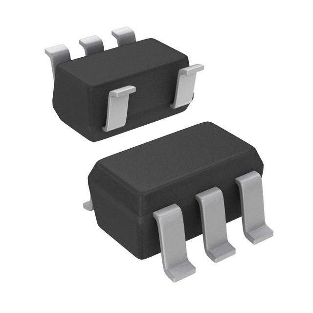
TPS73201-Q1 TPS73225-Q1 www.ti.com SGLS303E–MAY2005–REVISEDAUGUST2013 CAP-FREE NMOS 250-mA LOW-DROPOUT REGULATOR WITH REVERSE-CURRENT PROTECTION CheckforSamples:TPS73201-Q1,TPS73225-Q1 FEATURES APPLICATIONS 1 • QualifiedforAutomotiveApplications • Portable/Battery-PoweredEquipment • StablewithNoOutputCapacitororAnyValue • Post-RegulationforSwitchingSupplies orTypeofCapacitor • Noise-SensitiveCircuitrySuchasVCOs • InputVoltageRange:1.7Vto5.5V • PointofLoadRegulationforDSPs,FPGAs, • UltralowDropoutVoltage: ASICs,andMicroprocessors 40mVTypat250mA DESCRIPTION • ExcellentLoadTransientResponse—Withor WithoutOptionalOutputCapacitor The TPS732xx family of low-dropout (LDO) voltage regulators uses a new topology: an NMOS pass • NewNMOSTopologyProvidesLowReverse element in a voltage-follower configuration. This LeakageCurrent topology is stable using output capacitors with low • LowNoise:30μVRMSTyp(10kHzto100kHz) ESR, and even allows operation without a capacitor. • 0.5%InitialAccuracy It also provides high reverse blockage (low reverse current)andgroundpincurrentthatisnearlyconstant • 1%OverallAccuracy(Line,Load,and overallvaluesofoutputcurrent. Temperature) • LessThan1μAMaxI inShutdownMode The TPS732xx uses an advanced BiCMOS process Q to yield high precision while delivering low dropout • ThermalShutdownandSpecifiedMin/Max voltages and low ground pin current. Current CurrentLimitProtection consumption, when not enabled, is under 1 μA and • AvailableinMultipleOutputVoltageVersions ideal for portable applications. The extremely low output noise (30 μV with 0.1 µF C ) is ideal for – FixedOutputsof1.2V,1.5V,1.6V,1.8V, RMS NR powering VCOs. These devices are protected by 2.5V,3V,3.3V,and5V thermalshutdownandfoldbackcurrentlimit. – AdjustableOutputsFrom1.2Vto5.5V – CustomOutputsAvailable DBVPACKAGE Optional Optional (TOPVIEW) VIN IN OUT VOUT TPS732xx IN 1 5 OUT EN GND NR GND 2 EN 3 4 NR/FB Optional DRBPACKAGE Typical Application Circuit for Fixed-VoltageVersions (TOPVIEW) Figure1. OUT 1 8 IN N/C 2 7 N/C NR/FB 3 6 N/C GND 4 5 EN 1 Pleasebeawarethatanimportantnoticeconcerningavailability,standardwarranty,anduseincriticalapplicationsof TexasInstrumentssemiconductorproductsanddisclaimerstheretoappearsattheendofthisdatasheet. UNLESS OTHERWISE NOTED this document contains Copyright©2005–2013,TexasInstrumentsIncorporated PRODUCTION DATA information current as of publication date. Products conform to specifications per the terms of Texas Instruments standard warranty. Production processing does not necessarilyincludetestingofallparameters.
TPS73201-Q1 TPS73225-Q1 SGLS303E–MAY2005–REVISEDAUGUST2013 www.ti.com ORDERINGINFORMATION(1) TJ (TVYOPU)T(2) PACKAGE(3) ORDERABLEPARTNUMBER TOP-SIDEMARKING Adjustable SOT23-5–DBV Reelof3000 TPS73201QDBVRQ1 PJOQ –40°Cto125°C or1.2V(4) VSON-8–DRB Reelof3000 TPS73201QDRBRQ1 PSAQ 2.5V SOT23-5–DBV Reelof3000 TPS73225QDBVRQ1 PJNQ (1) Forthemostcurrentpackageandorderinginformation,seethePackageOptionAddendumattheendofthisdocument,orseetheTI websiteatwww.ti.com. (2) Customoutputvoltagesfrom1.3Vto4Vin100-mVincrementsareavailableonaquick-turnbasisforprototyping.Production quantitiesareavailable;minimumorderquantitiesapply.ContactTexasInstrumentsfordetailsandavailability. (3) Packagedrawings,thermaldata,andsymbolizationareavailableatwww.ti.com/packaging. (4) Forfixed1.2-Voperation,tieFBtoOUT. ABSOLUTE MAXIMUM RATINGS overoperatingjunctiontemperaturerangeunlessotherwisenoted(1) TPS732xx UNIT V range –0.3to6 V IN V range –0.3to6 V EN V range –0.3to5.5 V OUT Peakoutputcurrent Internallylimited Outputshort-circuitduration Indefinite Continuoustotalpowerdissipation SeePowerDissipationRatings Junctiontemperaturerange,T –55to+150 °C J Storagetemperaturerange –65to+150 °C ESDrating,HBM(2) (H2)4 kV ESDrating,CDM(2) (C4)1 kV ESDrating,MM(2) (M2)200 V (1) Stressesbeyondthoselistedunderabsolutemaximumratingsmaycausepermanentdamagetothedevice.Thesearestressratings only,andfunctionaloperationofthedeviceattheseoranyotherconditionsbeyondthoseindicatedundertheElectricalCharacteristics isnotimplied.Exposuretoabsolutemaximumratedconditionsforextendedperiodsmayaffectdevicereliability. (2) ESDProtectionLevelperAECQ100Classification 2 SubmitDocumentationFeedback Copyright©2005–2013,TexasInstrumentsIncorporated ProductFolderLinks:TPS73201-Q1TPS73225-Q1
TPS73201-Q1 TPS73225-Q1 www.ti.com SGLS303E–MAY2005–REVISEDAUGUST2013 THERMAL INFORMATION TPS732xx-Q1(3) THERMALMETRIC(1)(2) DRB DBV UNITS 8PINS 5PINS θ Junction-to-ambientthermalresistance(4) 47.8 180 JA θ Junction-to-case(top)thermalresistance(5) 83 64 JCtop θ Junction-to-boardthermalresistance(6) N/A 35 JB °C/W ψ Junction-to-topcharacterizationparameter(7) 2.1 N/A JT ψ Junction-to-boardcharacterizationparameter(8) 17.8 N/A JB θ Junction-to-case(bottom)thermalresistance(9) 12.1 N/A JCbot (1) Formoreinformationabouttraditionalandnewthermalmetrics,seetheICPackageThermalMetricsapplicationreport,SPRA953A. (2) ForthermalestimatesofthisdevicebasedonPCBcopperarea,seetheTIPCBThermalCalculator. (3) ThermaldatafortheDRBandDRVpackagesarederivedbythermalsimulationsbasedonJEDEC-standardmethodologyasspecified intheJESD51series.Thefollowingassumptionsareusedinthesimulations: (a)(a)DRB:TheexposedpadisconnectedtothePCBgroundlayerthrougha2x2thermalviaarray. (b)DBV:ThereisnoexposedpadwiththeDBVpackage. (b)(a)DRB:Thetopandbottomcopperlayersareassumedtohavea20%thermalconductivityofcopperrepresentinga20%copper coverage. (b)DBV:Thetopandbottomcopperlayersareassumedtohavea20%thermalconductivityofcopperrepresentinga20%copper coverage. (c)ThesedataweregeneratedwithonlyasingledeviceatthecenterofaJEDEChigh-K(2s2p)boardwith3-in×3-incopperarea.To understandtheeffectsofthecopperareaonthermalperformance,seethePowerDissipationsectionofthisdatasheet. (4) Thejunction-to-ambientthermalresistanceundernaturalconvectionisobtainedinasimulationonaJEDEC-standard,high-Kboard,as specifiedinJESD51-7,inanenvironmentdescribedinJESD51-2a. (5) Thejunction-to-case(top)thermalresistanceisobtainedbysimulatingacoldplatetestonthetopofthepackage.NospecificJEDEC- standardtestexists,butaclosedescriptioncanbefoundintheANSISEMIstandardG30-88. (6) Thejunction-to-boardthermalresistanceisobtainedbysimulatinginanenvironmentwitharingcoldplatefixturetocontrolthePCB temperature,asdescribedinJESD51-8. (7) Thejunction-to-topcharacterizationparameter,ψ ,estimatesthejunctiontemperatureofadeviceinarealsystemandisextracted JT fromthesimulationdatatoobtainθ usingaproceduredescribedinJESD51-2a(sections6and7). JA (8) Thejunction-to-boardcharacterizationparameter,ψ ,estimatesthejunctiontemperatureofadeviceinarealsystemandisextracted JB fromthesimulationdatatoobtainθ usingaproceduredescribedinJESD51-2a(sections6and7). JA (9) Thejunction-to-case(bottom)thermalresistanceisobtainedbysimulatingacoldplatetestontheexposed(power)pad.Nospecific JEDECstandardtestexists,butaclosedescriptioncanbefoundintheANSISEMIstandardG30-88. POWER DISSIPATION RATINGS(1) DERATINGFACTOR T ≤25°C T =70°C T =85°C BOARD PACKAGE R R A A A θJC θJA ABOVET =25°C POWERRATING POWERRATING POWERRATING A Low-K (2) DBV 64°C/W 255°C/W 3.9mW/°C 390mW 215mW 155mW High-K(3) DBV 64°C/W 180°C/W 5.6mW/°C 560mW 310mW 225mW High-K (3) DRB 1.2°C/W 40°C/W 25.0mW/°C 2.50W 1.38W 1W (1) SeePowerDissipationintheApplicationInformationsectionformoreinformationrelatedtothermaldesign. (2) TheJEDECLow-K(1s)boarddesignusedtoderivethisdatawasa3-inch×3-inch,two-layerboardwith2-ouncecoppertracesontop oftheboard. (3) TheJEDECHigh-K(2s2p)boarddesignusedtoderivethisdatawasa3inchx3inch,multilayerboardwith1-ounceinternalpowerand groundplanesand2-ouncecoppertracesonthetopandbottomoftheboard. Copyright©2005–2013,TexasInstrumentsIncorporated SubmitDocumentationFeedback 3 ProductFolderLinks:TPS73201-Q1TPS73225-Q1
TPS73201-Q1 TPS73225-Q1 SGLS303E–MAY2005–REVISEDAUGUST2013 www.ti.com ELECTRICAL CHARACTERISTICS Overoperatingtemperaturerange(T =–40°Cto125°C),V =V +0.5V(1),I =10mA,V =1.7V,and J IN OUT(nom) OUT EN C =0.1μF,unlessotherwisenoted.TypicalvaluesareatT =25°C OUT J PARAMETER TESTCONDITIONS MIN TYP MAX UNIT V Inputvoltagerange(1) 1.7 5.5 V IN V Internalreference(TPS73201) T =25°C 1.198 1.2 1.21 V FB J Outputvoltagerange(TPS73201)(2) V 5.5–V V FB DO Accuracy(1) Nominal T =25°C –0.5% +0.5% V J OUT (V +0.5V)≤V ≤5.5V, V ,I ,andT OUT IN –1% ±0.5% +1% IN OUT J 10mA≤I ≤250mA OUT ΔV %/ΔV Lineregulation(1) (V +0.5V)≤V ≤5.5V 0.06 %/V OUT IN OUT(nom) IN 1mA≤I ≤250mA 0.002 OUT ΔV %/ΔI Loadregulation %/mA OUT OUT 10mA≤I ≤250mA 0.0008 OUT Dropoutvoltage(3) V I =250mA 40 150 mV DO (V =V (nom)–0.1V) OUT IN OUT Z (DO) Outputimpedanceindropout 1.7V≤V ≤(V +V ) 0.25 Ω O IN OUT DO I Outputcurrentlimit V =0.9×V 250 425 600 mA CL OUT OUT(nom) I Short-circuitcurrent V =0V 300 mA SC OUT I Reverseleakagecurrent(4)(–I ) V ≤0.5V,0V≤V ≤V 0.1 10 μA REV IN EN IN OUT I =10mA(I ) 400 550 OUT Q I Groundpincurrent μA GND I =250mA 650 950 OUT I Shutdowncurrent(I ) V ≤0.5V,V ≤V ≤5.5 0.02 1 μA SHDN GND EN OUT IN Power-supplyrejectionratio f=100Hz,IOUT=250mA 58 PSRR dB (ripplerejection) f=10kHz,I =250mA 37 OUT Outputnoisevoltage COUT=10μF,NoCNR 27×VOUT V μV N BW=10Hz–100kHz C =10μF,C =0.01μF 8.5×V RMS OUT NR OUT V =3V,R =30Ω t Startuptime OUT L 600 μs STR C =1μF,C =0.01μF OUT NR V (HI) Enablehigh(enabled) 1.7 V V EN IN V (LO) Enablelow(shutdown) 0 0.5 V EN I (HI) Enablepincurrent(enabled) V =5.5V 0.02 0.1 μA EN EN Shutdown, Temperatureincreasing 160 T Thermalshutdowntemperature °C SD Reset, Temperaturedecreasing 140 (1) MinimumV =V +V or1.7V,whicheverisgreater. IN OUT DO (2) TPS73201istestedatV =2.5V. OUT (3) V isnotmeasuredfortheTPS73215orTPS73216,becauseminimumV =1.7V. DO IN (4) Fixed-voltageversionsonly;seetheApplicationInformationsectionformoreinformation. 4 SubmitDocumentationFeedback Copyright©2005–2013,TexasInstrumentsIncorporated ProductFolderLinks:TPS73201-Q1TPS73225-Q1
TPS73201-Q1 TPS73225-Q1 www.ti.com SGLS303E–MAY2005–REVISEDAUGUST2013 FUNCTIONALBLOCKDIAGRAMS IN Charge Pump EN Thermal Protection Ref Servo 27kW Bandgap Error Amp Current Limit OUT 8kW GND R 1 R1+R2=80kW R2 NR Figure2. FixedVoltageVersion IN Table 1. Standard 1% Resistor Values for Common Output Voltages VOUT R1 R2 Charge 1.2V Short Open Pump 1.5V 23.2kW 95.3kW EN Thermal 1.8V 28.0kW 56.2kW Protection 2.5V 39.2kW 36.5kW Ref Servo 2.8V 44.2kW 33.2kW 27kW 3.0V 46.4kW 30.9kW Bandgap Error 3.3V 52.3kW 30.1kW Amp 5.0V 78.7kW 24.9kW OUT Current Limit NOTE: VOUT = (R1 + R2)/R2 × 1.204; GND 8kW 80kW R1R2 @ 19kW for best R accuracy. 1 FB R 2 Figure3. AdjustableVoltageVersion Copyright©2005–2013,TexasInstrumentsIncorporated SubmitDocumentationFeedback 5 ProductFolderLinks:TPS73201-Q1TPS73225-Q1
TPS73201-Q1 TPS73225-Q1 SGLS303E–MAY2005–REVISEDAUGUST2013 www.ti.com PIN ASSIGNMENTS DBVPACKAGE DRBPACKAGE (TOPVIEW) (TOPVIEW) OUT 1 8 IN IN 1 5 OUT N/C 2 7 N/C GND 2 NR/FB 3 6 N/C GND 4 5 EN EN 3 4 NR/FB TERMINALFUNCTIONS TERMINAL NO. DESCRIPTION NAME DBV DRB IN 1 8 Unregulatedinputsupply GND 2 4,Pad Ground Drivingtheenablepin(EN)highturnsontheregulator.Drivingthispinlowputstheregulatorinto EN 3 5 shutdownmode.SeetheShutdownsectionunderApplicationsInformationformoredetails.ENcanbe connectedtoINifnotused. Fixedvoltageversionsonly—connectinganexternalcapacitortothispinbypassesnoisegeneratedbythe NR 4 3 internalbandgap.Thisallowsoutputnoisetobereducedtolowlevels. Adjustablevoltageversiononly—thisistheinputtothecontrollooperroramplifier,andisusedtosetthe FB 4 3 outputvoltageofthedevice. NC — 2,6,7 Nointernalconnection OUT 5 1 Outputoftheregulator.Therearenooutputcapacitorrequirementsforstability. 6 SubmitDocumentationFeedback Copyright©2005–2013,TexasInstrumentsIncorporated ProductFolderLinks:TPS73201-Q1TPS73225-Q1
TPS73201-Q1 TPS73225-Q1 www.ti.com SGLS303E–MAY2005–REVISEDAUGUST2013 TYPICAL CHARACTERISTICS ForallvoltageversionsatT =25°C,V =V +0.5V,I =10mA,V =1.7V,andC =0.1μF,unlessotherwise J IN OUT(nom) OUT EN OUT noted LOADREGULATION LINEREGULATION 0.5 0.20 0.4 ReferredtoIOUT=10mA ReferredtoVIN=VOUT+0.5VatIOUT=10mA 0.15 0.3 - 40(cid:1)C +25(cid:1)C 0.10 (%) 0.2 +125(cid:1)C (%) +125(cid:1)C +25(cid:1)C UT 0.1 UT 0.05 O O V V n 0 n 0 i i nge - 0.1 nge - 0.05 ha - 0.2 ha - 40(cid:1)C C C - 0.10 - 0.3 - 0.4 - 0.15 - 0.5 - 0.20 0 50 100 150 200 250 0 0.5 1.0 1.5 2.0 2.5 3.0 3.5 4.0 4.5 IOUT(mA) VIN- VOUT(V) Figure4. Figure5. DROPOUTVOLTAGE DROPOUTVOLTAGE vs vs OUTPUTCURRENT TEMPERATURE 100 100 TPS73225DBV TPS73225DBV 80 80 +125(cid:1)C V) 60 V) 60 m m ( ( VDO 40 +25(cid:1)C VDO 50 20 20 - 40(cid:1)C 0 0 0 50 100 150 200 250 - 50 - 25 0 25 50 75 100 125 IOUT(mA) Temperature((cid:1)C) Figure6. Figure7. OUTPUTVOLTAGEACCURACYHISTOGRAM OUTPUTVOLTAGEDRIFTHISTOGRAM 30 18 I =10mA I =10mA OUT OUT 16 AllVoltageVersions 25 14 %) %) ( 20 ( 12 s s nit nit 10 U U of 15 of 8 nt nt e e c 10 c 6 er er P P 4 5 2 0 0 098765432101234567890 000000000000000000000 1.0.0.0.0.0.0.0.0.0. 0.0.0.0.0.0.0.0.0.1. 10987654321 12345678910 --------V--Error(%) -----W-o-rst-Ca-se-dV /dT(ppm/(cid:1)C) OUT OUT Figure8. Figure9. Copyright©2005–2013,TexasInstrumentsIncorporated SubmitDocumentationFeedback 7 ProductFolderLinks:TPS73201-Q1TPS73225-Q1
TPS73201-Q1 TPS73225-Q1 SGLS303E–MAY2005–REVISEDAUGUST2013 www.ti.com TYPICAL CHARACTERISTICS (continued) ForallvoltageversionsatT =25°C,V =V +0.5V,I =10mA,V =1.7V,andC =0.1μF,unlessotherwise J IN OUT(nom) OUT EN OUT noted GROUNDPINCURRENT GROUNDPINCURRENT vs vs OUTPUTCURRENT TEMPERATURE 1000 800 I =250mA 900 700 OUT 800 600 700 500 A) 600 A) m( 500 m( 400 D D N N G400 G I I 300 300 V =5.5V 200 VIN=5.5V 200 VIINN=4V VIN=4V 100 VIN=2V 100 V =2V IN 0 0 0 50 100 150 200 250 - 50 - 25 0 25 50 75 100 125 IOUT(mA) Temperature((cid:1)C) Figure10. Figure11. CURRENTLIMIT vs GROUNDPINCURRENTINSHUTDOWN VOUT vs (FOLDBACK) TEMPERATURE 500 1 450 VENABLE=0.5V I V =V +0.5V 400 CL IN OUT A) 350 m mit( 300 ISC A) Li 250 m(D0.1 Current 210500 IGN 100 50 TPS73233 0 0.01 0 0.5 1.0 1.5 2.0 2.5 3.0 3.5 - 50 - 25 0 25 50 75 100 125 V (V) Temperature((cid:1)C) OUT Figure12. Figure13. CURRENTLIMIT CURRENTLIMIT vs vs V TEMPERATURE IN 600 600 550 550 A) 500 A) 500 m m ( ( mit 450 mit 450 Li Li nt 400 nt 400 e e urr urr C 350 C 350 300 300 250 250 1.5 2.0 2.5 3.0 3.5 4.0 4.5 5.0 5.5 - 50 - 25 0 25 50 75 100 125 V (V) Temperature((cid:1)C) IN Figure14. Figure15. 8 SubmitDocumentationFeedback Copyright©2005–2013,TexasInstrumentsIncorporated ProductFolderLinks:TPS73201-Q1TPS73225-Q1
TPS73201-Q1 TPS73225-Q1 www.ti.com SGLS303E–MAY2005–REVISEDAUGUST2013 TYPICAL CHARACTERISTICS (continued) ForallvoltageversionsatT =25°C,V =V +0.5V,I =10mA,V =1.7V,andC =0.1μF,unlessotherwise J IN OUT(nom) OUT EN OUT noted PSRR(RIPPLEREJECTION) PSRR(RIPPLEREJECTION) vs vs FREQUENCY V –V IN OUT 90 40 I =100mA I =1mA 80 COUT =Any COUT =1m F 35 OUT OUT 70 B) IOUT=1mA 30 Rejection(d 654000 ICOOUUTT==1AmnAy COUT=10m F IOC=O10=01mm AF SRR(dB) 2250 e P 15 pl 30 p Ri 20 IOUT=100mA 10 Frequency = 100kHz 10 IOUT=Any COUT=10m F 5 COUT = 10m F 0 COUT=0m F 0 CNR = 0.01m F 10 100 1k 10k 100k 1M 10M 0 0.2 0.4 0.6 0.8 1.0 1.2 1.4 1.6 1.8 2.0 Frequency(Hz) VIN- VOUT(V) Figure16. Figure17. NOISESPECTRALDENSITY NOISESPECTRALDENSITY C =0μF C =0.01μF NR NR 1 1 C =1m F OUT √Hz) COUT=0m F √Hz) COUT=1m F V/ 0.1 V/ 0.1 C =10m F m( OUT m( N N e e C =0m F OUT C =10m F OUT IOUT=150mA IOUT=150mA 0.01 0.01 10 100 1k 10k 100k 10 100 1k 10k 100k Frequency(Hz) Frequency(Hz) Figure18. Figure19. RMSNOISEVOLTAGE RMSNOISEVOLTAGE vs vs C C OUT NR 60 140 V =5.0V OUT 50 120 V =5.0V OUT 100 40 MS) MS) 80 VOUT=3.3V (RN 30 VOUT=3.3V (RN 60 V V 20 40 V =1.5V V =1.5V OUT OUT 10 CNR=0.01m F 20 COUT=0m F 10Hz<Frequency<100kHz 10Hz<Frequency<100kHz 0 0 0.1 1 10 1p 10p 100p 1n 10n C (m F) C (F) OUT NR Figure20. Figure21. Copyright©2005–2013,TexasInstrumentsIncorporated SubmitDocumentationFeedback 9 ProductFolderLinks:TPS73201-Q1TPS73225-Q1
TPS73201-Q1 TPS73225-Q1 SGLS303E–MAY2005–REVISEDAUGUST2013 www.ti.com TYPICAL CHARACTERISTICS (continued) ForallvoltageversionsatT =25°C,V =V +0.5V,I =10mA,V =1.7V,andC =0.1μF,unlessotherwise J IN OUT(nom) OUT EN OUT noted TPS73233 TPS73233 LOADTRANSIENTRESPONSE LINETRANSIENTRESPONSE VIN=3.8V COUT=0m F IOUT=250mA 50mV/tick V OUT C =0m F OUT 50mV/div V C =1m F OUT OUT 50mV/tick V OUT 50mV/tick COUT=10m F VOUT 50mV/div COUT=100m F VOUT dV 250mA 5.5V IN=0.5V/m s dt 50mA/tick 4.5V 10mA I 1V/div VIN OUT 10m s/div 10m s/div Figure22. Figure23. TPS73233 TPS73233 TURN-ONRESPONSE TURN-OFFRESPONSE RCLOU=T1=kW0m F VOUT RCLOU=T2=0W10m F 1V/div RCLOU=T2=0W1m F 1V/div RCLOU=T2=0W1m F R =1kW RCL=2=0W10m F CLOUT=0m F OUT V OUT 2V 2V V EN 1V/div 1V/div 0V 0V V EN 100m s/div 100m s/div Figure24. Figure25. I ENABLE TPS73233 vs POWERUP/POWERDOWN TEMPERATURE 6 10 5 V IN 4 V OUT 1 3 A) n s ( Volt 2 BLE A 1 EN I 0.1 0 - 1 - 2 0.01 50ms/div - 50 - 25 0 25 50 75 100 125 Temperature (°C) Figure26. Figure27. 10 SubmitDocumentationFeedback Copyright©2005–2013,TexasInstrumentsIncorporated ProductFolderLinks:TPS73201-Q1TPS73225-Q1
TPS73201-Q1 TPS73225-Q1 www.ti.com SGLS303E–MAY2005–REVISEDAUGUST2013 TYPICAL CHARACTERISTICS (continued) ForallvoltageversionsatT =25°C,V =V +0.5V,I =10mA,V =1.7V,andC =0.1μF,unlessotherwise J IN OUT(nom) OUT EN OUT noted TPS73201 TPS73201 RMSNOISEVOLTAGE I FB vs vs C TEMPERATURE ADJ 60 160 55 140 50 120 45 100 V(rms)N 4305 I(nA)FB 8600 V =2.5V 30 COUT=0m F 40 OUT 25 R1=39.2kW 20 10Hz<Frequency<100kHz 20 0 10p 100p 1n 10n - 50 - 25 0 25 50 75 100 125 C (F) Temperature((cid:1)C) FB Figure28. Figure29. TPS73201 TPS73201 LOADTRANSIENT,ADJUSTABLEVERSION LINETRANSIENT,ADJUSTABLEVERSION C =10nF V =2.5V FB OUT R =39.2kW C =10nF 100mV/div 1 COUT=0m F VOUT 100mV/div COUT=0m F FB VOUT COUT=10m F COUT=10m F 100mV/div VOUT 100mV/div VOUT 4.5V 250mA 3.5V V IN 10mA I OUT 10m s/div 5m s/div Figure30. Figure31. Copyright©2005–2013,TexasInstrumentsIncorporated SubmitDocumentationFeedback 11 ProductFolderLinks:TPS73201-Q1TPS73225-Q1
TPS73201-Q1 TPS73225-Q1 SGLS303E–MAY2005–REVISEDAUGUST2013 www.ti.com APPLICATION INFORMATION The TPS732xx belongs to a family of new generation LDO regulators that use an NMOS pass transistor to achieve ultra-low-dropout performance, reverse current blockage, and freedom from output capacitor constraints. These features, combined with low noise and an enable input, make the TPS732xx ideal for portable applications. This regulator family offers a wide selection of fixed output voltage versions and an adjustable outputversion.Allversionshavethermalandover-currentprotection,includingfoldbackcurrentlimit. Figure 32 shows the basic circuit connections for the fixed voltage models. Figure 33 gives the connections for theadjustableoutputversion(TPS73201). Optionalinputcapacitor. Optionaloutputcapacitor. Mayimprovesource Mayimproveloadtransient, impedance,noise,orPSRR. noise,orPSRR. VIN IN OUT VOUT TPS732xx EN GND NR Optionalbypass capacitortoreduce outputnoise. Figure32. TypicalApplicationCircuitforFixed-VoltageVersions Optionalinputcapacitor. Optionaloutputcapacitor. Mayimprovesource Mayimproveloadtransient, impedance,noise,orPSRR. noise,orPSRR. VIN IN OUT VOUT TPS732xx R C 1 FB EN GND FB R 2 (R +R) Optionalcapacitor VOUT= 1R 2 ×1.204 reducesoutputnoise. 2 Figure33. TypicalApplicationCircuitfor Adjustable-VoltageVersions R and R can be calculated for any output voltage using the formula shown in Figure 33. Sample resistor values 1 2 for common output voltages are shown in Figure 3. For best accuracy, make the parallel combination of R and 1 R approximately19kΩ. 2 Input and Output Capacitor Requirements Althoughaninputcapacitorisnotrequiredforstability,itisgoodanalogdesignpracticetoconnecta0.1-μFto1- μF low ESR capacitor across the input supply near the regulator. This counteracts reactive input sources and improves transient response, noise rejection, and ripple rejection. A higher-value capacitor may be necessary if large,fastrise-timeloadtransientsareanticipatedorthedeviceislocatedseveralinchesfromthepowersource. The TPS732xx does not require an output capacitor for stability and has maximum phase margin with no capacitor. It is designed to be stable for all available types and values of capacitors. In applications where V – V < 0.5 V and multiple low ESR capacitors are in parallel, ringing may occur when the product of C IN OUT OUT and total ESR drops below 50 nF. Total ESR includes all parasitic resistances, including capacitor ESR and board, socket, and solder joint resistance. In most applications, the sum of capacitor ESR and trace resistance willmeetthisrequirement. 12 SubmitDocumentationFeedback Copyright©2005–2013,TexasInstrumentsIncorporated ProductFolderLinks:TPS73201-Q1TPS73225-Q1
TPS73201-Q1 TPS73225-Q1 www.ti.com SGLS303E–MAY2005–REVISEDAUGUST2013 Output Noise A precision band-gap reference is used to generate the internal reference voltage, V . This reference is the REF dominant noise source within the TPS732xx and it generates approximately 32 μV (10 Hz to 100 kHz) at the RMS reference output (NR). The regulator control loop gains up the reference noise with the same gain as the referencevoltage,sothatthenoisevoltageoftheregulatorisapproximatelygivenby: (R (cid:2)R ) V V (cid:3)32(cid:1)V (cid:1) 1 2 (cid:3)32(cid:1)V (cid:1) OUT N RMS R2 RMS VREF (1) SincethevalueofV is1.2V,thisrelationshipreducesto: REF (cid:3)(cid:1)V (cid:4) VN((cid:1)VRMS)(cid:2)27 VRMS (cid:1)VOUT(V) (2) forthecaseofnoC . NR An internal 27-kΩ resistor in series with the noise reduction pin (NR) forms a low-pass filter for the voltage reference when an external noise reduction capacitor, C , is connected from NR to ground. For C = 10 nF, NR NR the total noise in the 10-Hz to 100-kHz bandwidth is reduced by a factor of ~3.2, giving the approximate relationship: (cid:3)(cid:1)V (cid:4) VN((cid:1)VRMS)(cid:2)8.5 VRMS (cid:1)VOUT(V) (3) forC =10nF. NR ThisnoisereductioneffectisshownasRMSNoiseVoltagevsC intheTypicalCharacteristicssection. NR The TPS73201 adjustable version does not have the noise-reduction pin available. However, connecting a feedback capacitor, C , from the output to the FB pin will reduce output noise and improve load transient FB performance. The TPS732xx uses an internal charge pump to develop an internal supply voltage sufficient to drive the gate of the NMOS pass element above V . The charge pump generates ~250 μV of switching noise at ~2 MHz; OUT however, charge-pump noise contribution is negligible at the output of the regulator for most values of I and OUT C . OUT Board Layout Recommendation to Improve PSRR and Noise Performance To improve ac performance such as PSRR, output noise, and transient response, it is recommended that the PCB be designed with separate ground planes for V and V , with each ground plane connected only at the IN OUT GND pin of the device. In addition, the ground connection for the bypass capacitor should connect directly to the GNDpinofthedevice. Internal Current Limit The TPS732xx internal current limit helps protect the regulator during fault conditions. Foldback helps to protect the regulator from damage during output short-circuit conditions by reducing current limit when V drops below OUT 0.5V.SeeFigure12intheTypicalCharacteristicssectionforagraphofI vsV . OUT OUT Shutdown The Enable pin is active high and is compatible with standard TTL-CMOS levels. V below 0.5 V (max) turns EN the regulator off and drops the ground pin current to approximately 10 nA. When shutdown capability is not required, the Enable pin can be connected to V . When a pullup resistor is used, and operation down to 1.8 V is IN required,usepullupresistorvaluesbelow50kΩ. Copyright©2005–2013,TexasInstrumentsIncorporated SubmitDocumentationFeedback 13 ProductFolderLinks:TPS73201-Q1TPS73225-Q1
TPS73201-Q1 TPS73225-Q1 SGLS303E–MAY2005–REVISEDAUGUST2013 www.ti.com Dropout Voltage The TPS732xx uses an NMOS pass transistor to achieve extremely low dropout. When (V – V ) is less than IN OUT the dropout voltage (V ), the NMOS pass device is in its linear region of operation and the input-to-output DO resistanceistheR oftheNMOSpasselement. DS-ON For large step changes in load current, the TPS732xx requires a larger voltage drop from V to V to avoid IN OUT degraded transient response. The boundary of this transient dropout region is approximately twice the dc dropout.ValuesofV –V abovethislineensurenormaltransientresponse. IN OUT Operating in the transient dropout region can cause an increase in recovery time. The time required to recover from a load transient is a function of the magnitude of the change in load current rate, the rate of change in load current, and the available headroom (V to V voltage drop). Under worst-case conditions [full-scale IN OUT instantaneous load change with (V – V ) close to dc dropout levels], the TPS732xx can take a couple of IN OUT hundredmicrosecondstoreturntothespecifiedregulationaccuracy. Transient Response The low open-loop output impedance provided by the NMOS pass element in a voltage follower configuration allows operation without an output capacitor for many applications. As with any regulator, the addition of a capacitor (nominal value 1 μF) from the output pin to ground will reduce undershoot magnitude but increase duration. In the adjustable version, the addition of a capacitor, C , from the output to the adjust pin will also FB improvethetransientresponse. The TPS732xx does not have active pulldown when the output is over-voltage. This allows applications that connect higher voltage sources, such as alternate power supplies, to the output. This also results in an output overshootofseveralpercentiftheloadcurrentquicklydropstozerowhenacapacitorisconnectedtotheoutput. The duration of overshoot can be reduced by adding a load resistor. The overshoot decays at a rate determined byoutputcapacitorC andtheinternal/externalloadresistance.Therateofdecayisgivenby: OUT (Fixedvoltageversion) V dV(cid:3)dt(cid:2) OUT C (cid:1)80k(cid:1) OUT (4) (Adjustablevoltageversion) V dV(cid:5)dt(cid:3) OUT C (cid:1)80k(cid:1)(cid:4)(R (cid:2)R ) OUT 1 2 (5) Reverse Current The NMOS pass element of the TPS732xx provides inherent protection against current flow from the output of the regulator to the input when the gate of the pass device is pulled low. To ensure that all charge is removed from the gate of the pass element, the enable pin must be driven low before the input voltage is removed. If this isnotdone,thepasselementmaybeleftonduetostoredchargeonthegate. After the enable pin is driven low, no bias voltage is needed on any pin for reverse current blocking. Note that reverse current is specified as the current flowing out of the IN pin due to voltage applied on the OUT pin. There will be additional current flowing into the OUT pin due to the 80-kΩ internal resistor divider to ground (see Figure2 andFigure3). FortheTPS73201,reversecurrentmayflowwhenV ismorethan1VaboveV . FB IN 14 SubmitDocumentationFeedback Copyright©2005–2013,TexasInstrumentsIncorporated ProductFolderLinks:TPS73201-Q1TPS73225-Q1
TPS73201-Q1 TPS73225-Q1 www.ti.com SGLS303E–MAY2005–REVISEDAUGUST2013 Thermal Protection Thermal protection disables the output when the junction temperature rises to approximately 160°C, allowing the device to cool. When the junction temperature cools to approximately 140°C, the output circuitry is again enabled. Depending on power dissipation, thermal resistance, and ambient temperature, the thermal protection circuit may cycle on and off. This limits the dissipation of the regulator, protecting it from damage due to overheating. Any tendency to activate the thermal protection circuit indicates excessive power dissipation or an inadequate heatsink. For reliable operation, junction temperature should be limited to 125°C maximum. To estimate the margin of safety in a complete design (including heatsink), increase the ambient temperature until the thermal protection is triggered; use worst-case loads and signal conditions. For good reliability, thermal protection should trigger at least 35°C above the maximum expected ambient condition of your application. This produces a worst- casejunctiontemperatureof125°Catthehighestexpectedambienttemperatureandworst-caseload. The internal protection circuitry of the TPS732xx has been designed to protect against overload conditions. It was not intended to replace proper heatsinking. Continuously running the TPS732xx into thermal shutdown will degradedevicereliability. Power Dissipation The ability to remove heat from the die is different for each package type, presenting different considerations in the PCB layout. The PCB area around the device that is free of other components moves the heat from the device to the ambient air. Performance data for JEDEC low- and high-K boards are shown in the Power Dissipation Ratings table. Using heavier copper will increase the effectiveness in removing heat from the device. Theadditionofplatedthrough-holestoheat-dissipatinglayerswillalsoimprovetheheat-sinkeffectiveness. Power dissipation depends on input voltage and load conditions. Power dissipation is equal to the product of the outputcurrenttimesthevoltagedropacrosstheoutputpasselement(V toV ): IN OUT P (cid:3)(V (cid:2)V )(cid:1)I D IN OUT OUT (6) Power dissipation can be minimized by using the lowest possible input voltage necessary to assure the required outputvoltage. Package Mounting Solder pad footprint recommendations for the TPS732xx are presented in the Solder Pad Recommendations for Surface-Mount Devices (SBFA015) application bulletin, available from the Texas Instruments web site at www.ti.com. Copyright©2005–2013,TexasInstrumentsIncorporated SubmitDocumentationFeedback 15 ProductFolderLinks:TPS73201-Q1TPS73225-Q1
TPS73201-Q1 TPS73225-Q1 SGLS303E–MAY2005–REVISEDAUGUST2013 www.ti.com REVISION HISTORY ChangesfromRevisionD(March2009)toRevisionE Page • DeletedTPS73215-Q1,TPS73216-Q1,TPS73218-Q1,TPS73230-Q1,TPS73233-Q1,andTPS73250-Q1fromthe datasheet ............................................................................................................................................................................. 1 16 SubmitDocumentationFeedback Copyright©2005–2013,TexasInstrumentsIncorporated ProductFolderLinks:TPS73201-Q1TPS73225-Q1
PACKAGE OPTION ADDENDUM www.ti.com 24-Mar-2016 PACKAGING INFORMATION Orderable Device Status Package Type Package Pins Package Eco Plan Lead/Ball Finish MSL Peak Temp Op Temp (°C) Device Marking Samples (1) Drawing Qty (2) (6) (3) (4/5) TPS73225QDBVRQ1 OBSOLETE SOT-23 DBV 5 TBD Call TI Call TI -40 to 125 PJNQ (1) The marketing status values are defined as follows: ACTIVE: Product device recommended for new designs. LIFEBUY: TI has announced that the device will be discontinued, and a lifetime-buy period is in effect. NRND: Not recommended for new designs. Device is in production to support existing customers, but TI does not recommend using this part in a new design. PREVIEW: Device has been announced but is not in production. Samples may or may not be available. OBSOLETE: TI has discontinued the production of the device. (2) Eco Plan - The planned eco-friendly classification: Pb-Free (RoHS), Pb-Free (RoHS Exempt), or Green (RoHS & no Sb/Br) - please check http://www.ti.com/productcontent for the latest availability information and additional product content details. TBD: The Pb-Free/Green conversion plan has not been defined. Pb-Free (RoHS): TI's terms "Lead-Free" or "Pb-Free" mean semiconductor products that are compatible with the current RoHS requirements for all 6 substances, including the requirement that lead not exceed 0.1% by weight in homogeneous materials. Where designed to be soldered at high temperatures, TI Pb-Free products are suitable for use in specified lead-free processes. Pb-Free (RoHS Exempt): This component has a RoHS exemption for either 1) lead-based flip-chip solder bumps used between the die and package, or 2) lead-based die adhesive used between the die and leadframe. The component is otherwise considered Pb-Free (RoHS compatible) as defined above. Green (RoHS & no Sb/Br): TI defines "Green" to mean Pb-Free (RoHS compatible), and free of Bromine (Br) and Antimony (Sb) based flame retardants (Br or Sb do not exceed 0.1% by weight in homogeneous material) (3) MSL, Peak Temp. - The Moisture Sensitivity Level rating according to the JEDEC industry standard classifications, and peak solder temperature. (4) There may be additional marking, which relates to the logo, the lot trace code information, or the environmental category on the device. (5) Multiple Device Markings will be inside parentheses. Only one Device Marking contained in parentheses and separated by a "~" will appear on a device. If a line is indented then it is a continuation of the previous line and the two combined represent the entire Device Marking for that device. (6) Lead/Ball Finish - Orderable Devices may have multiple material finish options. Finish options are separated by a vertical ruled line. Lead/Ball Finish values may wrap to two lines if the finish value exceeds the maximum column width. Important Information and Disclaimer:The information provided on this page represents TI's knowledge and belief as of the date that it is provided. TI bases its knowledge and belief on information provided by third parties, and makes no representation or warranty as to the accuracy of such information. Efforts are underway to better integrate information from third parties. TI has taken and continues to take reasonable steps to provide representative and accurate information but may not have conducted destructive testing or chemical analysis on incoming materials and chemicals. TI and TI suppliers consider certain information to be proprietary, and thus CAS numbers and other limited information may not be available for release. In no event shall TI's liability arising out of such information exceed the total purchase price of the TI part(s) at issue in this document sold by TI to Customer on an annual basis. Addendum-Page 1
PACKAGE OPTION ADDENDUM www.ti.com 24-Mar-2016 OTHER QUALIFIED VERSIONS OF TPS73225-Q1 : •Enhanced Product: TPS73225-EP NOTE: Qualified Version Definitions: •Enhanced Product - Supports Defense, Aerospace and Medical Applications Addendum-Page 2
None
IMPORTANTNOTICE TexasInstrumentsIncorporatedanditssubsidiaries(TI)reservetherighttomakecorrections,enhancements,improvementsandother changestoitssemiconductorproductsandservicesperJESD46,latestissue,andtodiscontinueanyproductorserviceperJESD48,latest issue.Buyersshouldobtainthelatestrelevantinformationbeforeplacingordersandshouldverifythatsuchinformationiscurrentand complete.Allsemiconductorproducts(alsoreferredtohereinas“components”)aresoldsubjecttoTI’stermsandconditionsofsale suppliedatthetimeoforderacknowledgment. TIwarrantsperformanceofitscomponentstothespecificationsapplicableatthetimeofsale,inaccordancewiththewarrantyinTI’sterms andconditionsofsaleofsemiconductorproducts.TestingandotherqualitycontroltechniquesareusedtotheextentTIdeemsnecessary tosupportthiswarranty.Exceptwheremandatedbyapplicablelaw,testingofallparametersofeachcomponentisnotnecessarily performed. TIassumesnoliabilityforapplicationsassistanceorthedesignofBuyers’products.Buyersareresponsiblefortheirproductsand applicationsusingTIcomponents.TominimizetherisksassociatedwithBuyers’productsandapplications,Buyersshouldprovide adequatedesignandoperatingsafeguards. TIdoesnotwarrantorrepresentthatanylicense,eitherexpressorimplied,isgrantedunderanypatentright,copyright,maskworkright,or otherintellectualpropertyrightrelatingtoanycombination,machine,orprocessinwhichTIcomponentsorservicesareused.Information publishedbyTIregardingthird-partyproductsorservicesdoesnotconstitutealicensetousesuchproductsorservicesorawarrantyor endorsementthereof.Useofsuchinformationmayrequirealicensefromathirdpartyunderthepatentsorotherintellectualpropertyofthe thirdparty,oralicensefromTIunderthepatentsorotherintellectualpropertyofTI. ReproductionofsignificantportionsofTIinformationinTIdatabooksordatasheetsispermissibleonlyifreproductioniswithoutalteration andisaccompaniedbyallassociatedwarranties,conditions,limitations,andnotices.TIisnotresponsibleorliableforsuchaltered documentation.Informationofthirdpartiesmaybesubjecttoadditionalrestrictions. ResaleofTIcomponentsorserviceswithstatementsdifferentfromorbeyondtheparametersstatedbyTIforthatcomponentorservice voidsallexpressandanyimpliedwarrantiesfortheassociatedTIcomponentorserviceandisanunfairanddeceptivebusinesspractice. TIisnotresponsibleorliableforanysuchstatements. Buyeracknowledgesandagreesthatitissolelyresponsibleforcompliancewithalllegal,regulatoryandsafety-relatedrequirements concerningitsproducts,andanyuseofTIcomponentsinitsapplications,notwithstandinganyapplications-relatedinformationorsupport thatmaybeprovidedbyTI.Buyerrepresentsandagreesthatithasallthenecessaryexpertisetocreateandimplementsafeguardswhich anticipatedangerousconsequencesoffailures,monitorfailuresandtheirconsequences,lessenthelikelihoodoffailuresthatmightcause harmandtakeappropriateremedialactions.BuyerwillfullyindemnifyTIanditsrepresentativesagainstanydamagesarisingoutoftheuse ofanyTIcomponentsinsafety-criticalapplications. Insomecases,TIcomponentsmaybepromotedspecificallytofacilitatesafety-relatedapplications.Withsuchcomponents,TI’sgoalisto helpenablecustomerstodesignandcreatetheirownend-productsolutionsthatmeetapplicablefunctionalsafetystandardsand requirements.Nonetheless,suchcomponentsaresubjecttotheseterms. NoTIcomponentsareauthorizedforuseinFDAClassIII(orsimilarlife-criticalmedicalequipment)unlessauthorizedofficersoftheparties haveexecutedaspecialagreementspecificallygoverningsuchuse. OnlythoseTIcomponentswhichTIhasspecificallydesignatedasmilitarygradeor“enhancedplastic”aredesignedandintendedforusein military/aerospaceapplicationsorenvironments.BuyeracknowledgesandagreesthatanymilitaryoraerospaceuseofTIcomponents whichhavenotbeensodesignatedissolelyattheBuyer'srisk,andthatBuyerissolelyresponsibleforcompliancewithalllegaland regulatoryrequirementsinconnectionwithsuchuse. TIhasspecificallydesignatedcertaincomponentsasmeetingISO/TS16949requirements,mainlyforautomotiveuse.Inanycaseofuseof non-designatedproducts,TIwillnotberesponsibleforanyfailuretomeetISO/TS16949. Products Applications Audio www.ti.com/audio AutomotiveandTransportation www.ti.com/automotive Amplifiers amplifier.ti.com CommunicationsandTelecom www.ti.com/communications DataConverters dataconverter.ti.com ComputersandPeripherals www.ti.com/computers DLP®Products www.dlp.com ConsumerElectronics www.ti.com/consumer-apps DSP dsp.ti.com EnergyandLighting www.ti.com/energy ClocksandTimers www.ti.com/clocks Industrial www.ti.com/industrial Interface interface.ti.com Medical www.ti.com/medical Logic logic.ti.com Security www.ti.com/security PowerMgmt power.ti.com Space,AvionicsandDefense www.ti.com/space-avionics-defense Microcontrollers microcontroller.ti.com VideoandImaging www.ti.com/video RFID www.ti-rfid.com OMAPApplicationsProcessors www.ti.com/omap TIE2ECommunity e2e.ti.com WirelessConnectivity www.ti.com/wirelessconnectivity MailingAddress:TexasInstruments,PostOfficeBox655303,Dallas,Texas75265 Copyright©2016,TexasInstrumentsIncorporated