ICGOO在线商城 > 集成电路(IC) > PMIC - 稳压器 - 线性 > TPS78601KTTT
 Datasheet下载
- 型号: TPS78601KTTT
- 制造商: Texas Instruments
- 库位|库存: xxxx|xxxx
- 要求:
| 数量阶梯 | 香港交货 | 国内含税 |
| +xxxx | $xxxx | ¥xxxx |
查看当月历史价格
查看今年历史价格
TPS78601KTTT产品简介:
ICGOO电子元器件商城为您提供TPS78601KTTT由Texas Instruments设计生产,在icgoo商城现货销售,并且可以通过原厂、代理商等渠道进行代购。 TPS78601KTTT价格参考¥19.68-¥41.83。Texas InstrumentsTPS78601KTTT封装/规格:PMIC - 稳压器 - 线性, Linear Voltage Regulator IC Positive Adjustable 1 Output 1.2 V ~ 5.5 V 1.5A DDPAK/TO-263-5。您可以下载TPS78601KTTT参考资料、Datasheet数据手册功能说明书,资料中有TPS78601KTTT 详细功能的应用电路图电压和使用方法及教程。
TPS78601KTTT是德州仪器(Texas Instruments)生产的PMIC(电源管理集成电路),具体属于线性稳压器类别。该型号具有低功耗、高精度和小型封装的特点,适用于多种需要高效稳定电压输出的应用场景。

 主要应用场景:

1. 便携式电子设备:
   - TPS78601KTTT的低静态电流(Iq)使其非常适合用于电池供电的便携式设备,如智能手机、平板电脑、可穿戴设备等。它能够有效延长电池寿命,同时提供稳定的电压输出。

2. 物联网(IoT)设备:
   - 在IoT设备中,TPS78601KTTT可以为微控制器、传感器和其他低功耗组件提供稳定的电源。其小尺寸和低功耗特性使得它在空间受限且需要长时间运行的IoT应用中表现出色,例如智能家居设备、环境监测系统等。

3. 工业自动化与控制:
   - 在工业环境中,TPS78601KTTT可用于为各种传感器、执行器和通信模块提供稳定的电源。其宽输入电压范围(1.5V至5.5V)和高精度输出(±1%)确保了系统的可靠性和稳定性,适用于工厂自动化、机器人控制等领域。

4. 医疗设备:
   - 对于便携式医疗设备,如血糖仪、脉搏血氧仪等,TPS78601KTTT的低功耗和高精度特性非常重要。它可以确保设备在使用过程中保持稳定的性能,同时延长电池寿命,提高用户体验。

5. 无线通信模块:
   - 在无线通信模块中,TPS78601KTTT可以为射频(RF)芯片、蓝牙模块、Wi-Fi模块等提供稳定的电源。其快速瞬态响应能力有助于减少噪声干扰,确保通信质量。

 总结:
TPS78601KTTT凭借其低功耗、高精度和紧凑的设计,广泛应用于便携式电子设备、物联网、工业自动化、医疗设备和无线通信模块等领域。它不仅能够提供稳定的电压输出,还能有效延长电池寿命,满足现代电子设备对高效电源管理的需求。
| 参数 | 数值 |
| 产品目录 | 集成电路 (IC)半导体 |
| 描述 | IC REG LDO ADJ 1.5A DDPAK低压差稳压器 High PSRR Fast RF High-Enable 1.5A |
| 产品分类 | |
| 品牌 | Texas Instruments |
| 产品手册 | |
| 产品图片 |
|
| rohs | 符合RoHS无铅 / 符合限制有害物质指令(RoHS)规范要求 |
| 产品系列 | 电源管理 IC,低压差稳压器,Texas Instruments TPS78601KTTT- |
| 数据手册 | |
| 产品型号 | TPS78601KTTT |
| 产品目录页面 | |
| 产品种类 | 低压差稳压器 |
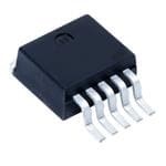
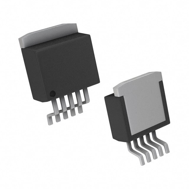
| 供应商器件封装 | DDPAK/TO-263-5 |
| 其它名称 | 296-14421-1 |
| 包装 | 剪切带 (CT) |
| 单位重量 | 1.456 g |
| 参考电压 | 1.225 V |
| 商标 | Texas Instruments |
| 安装类型 | 表面贴装 |
| 安装风格 | SMD/SMT |
| 封装 | Reel |
| 封装/外壳 | TO-263-6,D²Pak(5 引线+接片),TO-263BA |
| 封装/箱体 | TO-263-5 |
| 工作温度 | -40°C ~ 125°C |
| 工厂包装数量 | 50 |
| 最大工作温度 | + 125 C |
| 最大输入电压 | 5.5 V |
| 最小工作温度 | - 40 C |
| 最小输入电压 | + 2.7 V |
| 标准包装 | 1 |
| 电压-跌落(典型值) | 0.31V @ 1.5A |
| 电压-输入 | 2.7 V ~ 5.5 V |
| 电压-输出 | 1.2 V ~ 5.5 V |
| 电流-输出 | 1.5A |
| 电流-限制(最小值) | 2.4A |
| 稳压器拓扑 | 正,可调式 |
| 稳压器数 | 1 |
| 系列 | TPS78601 |
| 线路调整率 | 5 % / V |
| 负载调节 | 7 mV |
| 输入偏压电流—最大 | 0.31 mA |
| 输出电压 | 1.2 V to 5.5 V |
| 输出电流 | 1.5 A |
| 输出端数量 | 1 Output |
| 输出类型 | Adjustable |
| 配用 | /product-detail/zh/TPS78633EVM-207/296-20625-ND/562085/product-detail/zh/XILINXPWR-079/296-19048-ND/863869 |


.jpg)


- 商务部:美国ITC正式对集成电路等产品启动337调查
- 曝三星4nm工艺存在良率问题 高通将骁龙8 Gen1或转产台积电
- 太阳诱电将投资9.5亿元在常州建新厂生产MLCC 预计2023年完工
- 英特尔发布欧洲新工厂建设计划 深化IDM 2.0 战略
- 台积电先进制程称霸业界 有大客户加持明年业绩稳了
- 达到5530亿美元!SIA预计今年全球半导体销售额将创下新高
- 英特尔拟将自动驾驶子公司Mobileye上市 估值或超500亿美元
- 三星加码芯片和SET,合并消费电子和移动部门,撤换高东真等 CEO
- 三星电子宣布重大人事变动 还合并消费电子和移动部门
- 海关总署:前11个月进口集成电路产品价值2.52万亿元 增长14.8%


PDF Datasheet 数据手册内容提取
Product Sample & Technical Tools & Support & Folder Buy Documents Software Community TPS786 SLVS389M–SEPTEMBER2002–REVISEDSEPTEMBER2015 TPS786 Ultralow-Noise, High-PSRR, Fast, RF, 1.5-A Low-Dropout Linear Regulators 1 Features 3 Description • 1.5-ALow-DropoutRegulatorWithEnable The TPS786 family of low-dropout (LDO) low-power 1 linear voltage regulators features high power-supply • AvailableinFixedandAdjustable(1.2Vto5.5V) rejection ratio (PSRR), ultralow noise, fast start-up, OutputVersions and excellent line and load transient responses in • HighPSRR(49dBat10kHz) small outline, SOT223-6 and DDPAK-5 packages. • UltralowNoise(48μV ,TPS78630) Each device in the family is stable, with a small 1-μF RMS ceramic capacitor on the output. The family uses an • FastStart-UpTime(50 μs) advanced, proprietary BiCMOS fabrication process to • StableWitha1-μFCeramicCapacitor yield extremely low dropout voltages (for example, • ExcellentLoadandLineTransientResponse 390 mV at 1.5 A). Each device achieves fast start-up times (approximately 50 μs with a 0.001-μF bypass • VeryLowDropoutVoltage(390mVatFullLoad, capacitor) while consuming very low quiescent TPS78630) current (265 μA, typical). Moreover, when the device • 3× 3SONPowerPAD™,6-PinSOT223and5-Pin is placed in standby mode, the supply current is DDPAKPackage reduced to less than 1 μA. The TPS78630 exhibits approximately 48 μV of output voltage at 3-V RMS 2 Applications output noise with a 0.1-μF bypass capacitor. Applications with analog components that are noise • RF:VCOs,Receivers,ADCs sensitive, such as portable RF electronics, benefit • Audio from the high PSRR, low noise features, and the fast • Bluetooth®,WirelessLAN responsetime. • CellularandCordlessTelephones DeviceInformation(1) • HandheldOrganizers,PDAs PARTNUMBER PACKAGE BODYSIZE(NOM) TO-263(5) 10.16mm×8.42mm TPS786 SOT-223(6) 6.50mm×3.50mm SON(8) 3.00mm×3.00mm (1) For all available packages, see the orderable addendum at theendofthedatasheet. RippleRejectionvsFrequency OutputSpectralNoiseDensityvs 80 Frequency VIN=4V 70 COUT=10µF ction−(dB) 456000 IOIUOTUT==11m.5AA CNR=0.01µF ÖµVHz)nsity ( 000...678000 VCCIONNRU=T=5=0.5.21.V2µµFF eje De 0.50 pple R 30 Noise 0.40 Ri 20 ctral 0.30 IOUT=1mA 10 Spe 0.20 01 10 100 1k 10k 100k 1M 10M Output 0.10 IOUT=1.5A f (Hz) 0.00 100 1k 10k 100k Frequency (Hz) 1 An IMPORTANT NOTICE at the end of this data sheet addresses availability, warranty, changes, use in safety-critical applications, intellectualpropertymattersandotherimportantdisclaimers.PRODUCTIONDATA.
TPS786 SLVS389M–SEPTEMBER2002–REVISEDSEPTEMBER2015 www.ti.com Table of Contents 1 Features.................................................................. 1 8 ApplicationandImplementation........................ 13 2 Applications........................................................... 1 8.1 ApplicationInformation............................................13 3 Description............................................................. 1 8.2 TypicalApplication..................................................14 4 RevisionHistory..................................................... 2 9 PowerSupplyRecommendations...................... 16 5 PinConfigurationandFunctions......................... 3 10 Layout................................................................... 16 6 Specifications......................................................... 4 10.1 LayoutGuidelines.................................................16 6.1 AbsoluteMaximumRatings......................................4 10.2 LayoutExamples...................................................16 6.2 ESDRatings..............................................................4 10.3 RegulatorMounting...............................................17 6.3 RecommendedOperatingConditions.......................4 10.4 PowerDissipation.................................................17 6.4 ThermalInformation..................................................5 11 DeviceandDocumentationSupport................. 21 6.5 ElectricalCharacteristics...........................................6 11.1 DeviceSupport......................................................21 6.6 TypicalCharacteristics..............................................7 11.2 DocumentationSupport........................................21 7 DetailedDescription............................................ 11 11.3 CommunityResources..........................................21 7.1 Overview.................................................................11 11.4 Trademarks...........................................................21 7.2 FunctionalBlockDiagrams.....................................11 11.5 ElectrostaticDischargeCaution............................21 7.3 FeatureDescription.................................................12 11.6 Glossary................................................................22 7.4 DeviceFunctionalModes........................................12 12 Mechanical,Packaging,andOrderable Information........................................................... 22 4 Revision History NOTE:Pagenumbersforpreviousrevisionsmaydifferfrompagenumbersinthecurrentversion. ChangesfromRevisionL(October2010)toRevisionM Page • AddedESDRatingstable,FeatureDescriptionsection,DeviceFunctionalModes,ApplicationandImplementation section,PowerSupplyRecommendationssection,Layoutsection,DeviceandDocumentationSupportsection,and Mechanical,Packaging,andOrderableInformationsection ................................................................................................. 1 • UpdatedThermalInformation................................................................................................................................................. 5 ChangesfromRevisionK(August,2010)toRevisionL Page • CorrectedtypoinFigure34.................................................................................................................................................. 20 ChangesfromRevisionJ(May,2009)toRevisionK Page • ReplacedtheDissipationRatingstablewiththeThermalInformationTable......................................................................... 5 • Revisedsection.................................................................................................................................................................... 17 2 SubmitDocumentationFeedback Copyright©2002–2015,TexasInstrumentsIncorporated ProductFolderLinks:TPS786
TPS786 www.ti.com SLVS389M–SEPTEMBER2002–REVISEDSEPTEMBER2015 5 Pin Configuration and Functions DCQPackage 6-PinSOT-223 DRBPackage TopView 8-SON TopView EN 1 IN 1 8 EN IN 2 6 IN 2 7 NC GND 3 GND OUT 3 6 GND OUT 4 OUT 4 5 NR/FB NR/FB 5 KTTPackage 5-PinTO-263 TopView EN 1 IN 2 GND 3 OUT 4 NR/FB 5 PinFunctions PIN I/O DESCRIPTION NAME SOT-223 TO-263 SON Noise-reductionpinforfixedversionsonly.Anexternalbypasscapacitor,connectedtothis NR 5 5 5 — terminal,inconjunctionwithaninternalresistor,createsalow-passfiltertofurtherreduce regulatornoise. TheENterminalisaninputthatenablesorshutsdownthedevice.WhenENisalogichigh, EN 1 1 8 I thedeviceisenabled.Whenthedeviceisalogiclow,thedeviceisinshutdownmode. FB 5 5 5 I Feedbackinputvoltagefortheadjustabledevice. GND 3,6 3,TAB 6 — Regulatorground IN 2 2 1,2 I Inputsupply OUT 4 4 3,4 O Regulatoroutput Copyright©2002–2015,TexasInstrumentsIncorporated SubmitDocumentationFeedback 3 ProductFolderLinks:TPS786
TPS786 SLVS389M–SEPTEMBER2002–REVISEDSEPTEMBER2015 www.ti.com 6 Specifications 6.1 Absolute Maximum Ratings overoperatingfree-airtemperaturerange(unlessotherwisenoted)(1) MIN MAX UNIT V –0.3 6 V IN V –0.3 V +0.3 V EN IN V 6 V OUT Peakoutputcurrent Internallylimited Continuoustotalpowerdissipation SeeThermalInformation Junctiontemperature,T –40 150 °C J Storagetemperature,T –65 150 °C stg (1) StressesbeyondthoselistedunderAbsoluteMaximumRatingsmaycausepermanentdamagetothedevice.Thesearestressratings only,whichdonotimplyfunctionaloperationofthedeviceattheseoranyotherconditionsbeyondthoseindicatedunderRecommended OperatingConditions.Exposuretoabsolute-maximum-ratedconditionsforextendedperiodsmayaffectdevicereliability. 6.2 ESD Ratings VALUE UNIT Humanbodymodel(HBM),perANSI/ESDA/JEDECJS-001,allpins(1) ±2000 V(ESD) Electrostaticdischarge Chargeddevicemodel(CDM),perJEDECspecificationJESD22-C101,all V pins(2) ±500 (1) JEDECdocumentJEP155statesthat500-VHBMallowssafemanufacturingwithastandardESDcontrolprocess. (2) JEDECdocumentJEP157statesthat250-VCDMallowssafemanufacturingwithastandardESDcontrolprocess. 6.3 Recommended Operating Conditions overoperatingjunctiontemperaturerange(unlessotherwisenoted) MIN NOM MAX UNIT V Inputsupplyvoltage 2.7 5.5 V IN I Outputcurrent 0 1.5 A OUT T Operatingjunctiontemperature –40 125 °C J 4 SubmitDocumentationFeedback Copyright©2002–2015,TexasInstrumentsIncorporated ProductFolderLinks:TPS786
TPS786 www.ti.com SLVS389M–SEPTEMBER2002–REVISEDSEPTEMBER2015 6.4 Thermal Information TPS786(3) THERMALMETRIC(1)(2) DRB(SON) DCQ(S0T-223) KTT(TO-263) UNIT 8PINS 6PINS 5PINS R Junction-to-ambientthermalresistance 41.1 54.2 40.7 °C/W θJA R Junction-to-case(top)thermalresistance 49.1 33.3 43.1 °C/W θJC(top) R Junction-to-boardthermalresistance 16.6 8.9 21.5 °C/W θJB ψ Junction-to-topcharacterizationparameter 0.7 2.6 9.4 °C/W JT ψ Junction-to-boardcharacterizationparameter 16.8 8.8 20 °C/W JB R Junction-to-case(bottom)thermalresistance 5.2 N/A 2.1 °C/W θJC(bot) (1) Formoreinformationabouttraditionalandnewthermalmetrics,seetheSemiconductorandICPackageThermalMetricsapplication report,SPRA953. (2) ForthermalestimatesofthisdevicebasedonPCBcopperarea,seetheTIPCBThermalCalculator. (3) ThermaldatafortheDRB,DCQ,andDRVpackagesarederivedbythermalsimulationsbasedonJEDEC-standardmethodologyas specifiedintheJESD51series.Thefollowingassumptionsareusedinthesimulations: (a) i. DRB: The exposed pad is connected to the PCB ground layer through a 2×2 thermal via array. . ii. DCQ: The exposed pad is connected to the PCB ground layer through a 3×2 thermal via array. .iii.KTT:TheexposedpadisconnectedtothePCBgroundlayerthrougha5×4thermalviaarray. (b) i.DRB:Thetopandbottomcopperlayersareassumedtohavea20%thermalconductivityofcopperrepresentinga20%copper coverage. . ii. DCQ: Each of top and bottom copper layers has a dedicated pattern for 20% copper coverage. .iii.KTT:Thetopandbottomcopperlayersareassumedtohavea20%thermalconductivityofcopperrepresentinga20%copper coverage. (c)ThesedataweregeneratedwithonlyasingledeviceatthecenterofaJEDEChigh-K(2s2p)boardwith3inches×3inchescopper area. To understand the effects of the copper area on thermal performance, see the Power Dissipation and Estimating Junction Temperaturesectionsofthisdatasheet. Copyright©2002–2015,TexasInstrumentsIncorporated SubmitDocumentationFeedback 5 ProductFolderLinks:TPS786
TPS786 SLVS389M–SEPTEMBER2002–REVISEDSEPTEMBER2015 www.ti.com 6.5 Electrical Characteristics Overrecommendedoperatingtemperaturerange(T =–40°Cto125°C),V =V ,V =V +1V(1),I =1mA, J EN IN IN OUT(nom) OUT C =10μF,andC =0.01μF,unlessotherwisenoted.Typicalvaluesareat25°C. OUT NR PARAMETER TESTCONDITIONS MIN TYP MAX UNIT Inputvoltage,VIN(1) 2.7 5.5 V Internalreference,VFB(TPS78601) 1.200 1.225 1.250 V ContinuousoutputcurrentIOUT 0 1.5 A Outputvoltagerange TPS78601 1.225 5.5–VDO V TPS78601(2) 0μA≤IOUT≤1.5A,VOUT+1V≤VIN≤5.5V(1) (0.98)VOUT VOUT (1.02)VOUT V Ovoulttapguet Accuracy F<ix5eVdVOUT 0μA≤IOUT≤1.5A,VOUT+1V≤VIN≤5.5V(1) –2% 2% F=ix5eVdVOUT 0μA≤IOUT≤1.5A,VOUT+1V≤VIN≤5.5V(1) –3% 3% Outputvoltagelineregulation(ΔVOUT%/VIN)(1) VOUT+1V≤VIN≤5.5V 5 12 %/V Loadregulation(ΔVOUT%/VOUT) 0μA≤IOUT≤1.5A 7 mV TPS78628 IOUT=1.5A 410 580 Dropoutvoltage(3) TPS78630 IOUT=1.5A 390 550 mV VIN=VOUT(nom)–0.1V TPS78633 IOUT=1.5A 340 510 TPS78650 IOUT=1.5A 310 470 Outputcurrentlimit VOUT=0V 2.4 4.2 A Groundpincurrent 0μA≤IOUT≤1.5A 260 385 μA Shutdowncurrent(4) VEN=0V,2.7V≤VIN≤5.5V 0.07 1 μA FBpincurrent VFB=1.225V 1 μA f=100Hz,IOUT=10mA 59 f=100Hz,IOUT=1.5A 52 Power-supplyripplerejection TPS78630 dB f=10kHz,IOUT=1.5A 49 f=100kHz,IOUT=1.5A 32 CNR=0.001μF 66 BW=100Hzto100kHz, CNR=0.0047μF 51 Outputnoisevoltage(TPS78630) IOUT=1.5A CNR=0.01μF 49 μVRMS CNR=0.1μF 48 CNR=0.001μF 50 Time,start-up(TPS78630) RL=2Ω,COUT=1μF CNR=0.0047μF 75 μs CNR=0.01μF 110 High-levelenableinputvoltage 2.7V≤VIN≤5.5V 1.7 VIN V Low-levelenableinputvoltage 2.7V≤VIN≤5.5V 0 0.7 V ENpincurrent VEN=0 –1 1 μA UVLOthreshold VCCrising 2.25 2.65 V UVLOhysteresis 100 mV (1) MinimumV =V +V or2.7V,whicheverisgreater.TheTPS78650istestedatV =5.5V. IN OUT DO IN (2) Toleranceofexternalresistorsnotincludedinthisspecification. (3) DropoutisnotmeasuredforTPS78618orTPS78625becauseminimumV =2.7V. IN (4) Foradjustableversion,thisappliesonlyafterV isapplied;thenV transitionshightolow. IN EN 6 SubmitDocumentationFeedback Copyright©2002–2015,TexasInstrumentsIncorporated ProductFolderLinks:TPS786
TPS786 www.ti.com SLVS389M–SEPTEMBER2002–REVISEDSEPTEMBER2015 6.6 Typical Characteristics 3.05 2.7958 3.04 VIN=4V VIN=3.8V COUT=10µF COUT=10µF 3.03 TJ=25°C 2.7944 3.02 IOUT=1mA V) 3.01 V)2.7930 (UT 3.00 (UT O O V 2.99 V2.7826 2.98 IOUT=1.5A 2.97 2.7812 2.96 2.95 2.7708 0.0 0.3 0.6 0.9 1.2 1.5 −40−25−10 5 20 35 50 65 80 95110125 IOUT(A) TJ(°C) Figure1.TPS78630OutputVoltagevsOutputCurrent Figure2.TPS78628OutputVoltagevsJunction Temperature 350 340 VCIONU=T3=.810VµF ÖµVHz) 00..7800 VCCIONNRU=T=5=0.5.21.V2µµFF 330 nsity ( 0.60 A) De 0.50 µI(GND 331200 IOUT=1.5A ctral Noise 00..3400 IOUT=1mA e IOUT=1mA Sp 0.20 300 utput 0.10 IOUT=1.5A O 290 0.00 −40−25−10 5 20 35 50 65 80 95110125 100 1k 10k 100k TJ(°C) Frequency (Hz) Figure3.TPS78628GroundCurrentvsJunction Figure4.TPS78630OutputSpectralNoiseDensityvs Temperature Frequency 0.6 3.0 ÖµH)Vz 0.5 VCCIONNRU=T=5=0.5.110VµµFF ÖµHVz)( 2.5 VCIOIONUUT=T=5=1.51.50VAµF Output Spectral Noise Density ( 0000....1234 IOIUOTUT==11m.5AA Output Spectral Noise Density− 0112....5050 CNR=C0.N1CRµN=FR0=.0C00.N407R1µ=µFF0.001µF 0.0 0.0 100 1k 10k 100k 100 1k 10k 100k Frequency (Hz) Frequency (Hz) Figure5.TPS78630OutputSpectralNoiseDensityvs Figure6.TPS78630OutputSpectralNoiseDensityvs Frequency Frequency Copyright©2002–2015,TexasInstrumentsIncorporated SubmitDocumentationFeedback 7 ProductFolderLinks:TPS786
TPS786 SLVS389M–SEPTEMBER2002–REVISEDSEPTEMBER2015 www.ti.com Typical Characteristics (continued) 80 600 VIN=2.7V 70 500 COUT=10µF IOUT=1.5A )S 60 M R 400 µuVtput Noise ( 345000 V(mV)DO 230000 O S 20 RM 10 ICOOUUTT==11.50AµF 100 BW=100Hzto100kHz 0 0 0.001µF 0.0047µF 0.01µF 0.1µF −40−25−10 5 20 35 50 65 80 95110125 CNR(µF) TJ(°C) Figure7.TPS78630RootMeanSquaredOutputNoisevs Figure8.TPS78628DropoutVoltagevsJunction BypassCapacitance Temperature 80 80 VIN=4V VIN=4V 70 COUT=10µF 70 COUT=10µF IOUT=1mA CNR=0.01µF IOUT=1mA CNR=0.1µF Ripple Rejection−(dB) 2345600000 IOUT=1.5A Ripple Rejection (dB) 2345600000 IOUT=1.5A 10 10 0 0 1 10 100 1k 10k 100k 1M 10M 1 10 100 1k 10k 100k 1M 10M f (Hz) f (Hz) Figure9.TPS78630RippleRejectionvsFrequency Figure10.TPS78630RippleRejectionvsFrequency 80 80 VIN=4V VIN=4V 70 COUT=2.2µF 70 COUT=2.2µF IOUT=1mA CNR=0.01µF IOUT=1mA CNR=0.1µF B) 60 B) 60 Rejection (d 4500 IOUT=1.5A Rejection (d 4500 IOUT=1.5A Ripple 2300 Ripple 2300 10 10 0 0 1 10 100 1k 10k 100k 1M 10M 1 10 100 1k 10k 100k 1M 10M f (Hz) f (Hz) Figure11.TPS78630RippleRejectionvsFrequency Figure12.TPS78630RippleRejectionvsFrequency 8 SubmitDocumentationFeedback Copyright©2002–2015,TexasInstrumentsIncorporated ProductFolderLinks:TPS786
TPS786 www.ti.com SLVS389M–SEPTEMBER2002–REVISEDSEPTEMBER2015 Typical Characteristics (continued) 5 6 4 5 V(V)IN 3 V(V)IN 4 2 IOUT=1.5A dv 1V 3 IOUT=1.5A dv 1V COUT=10µF dt µs COUT=10µF dt µs 60 CNR=0.01µF 80 CNR=0.01µF 30 V) 40 mV) 0 (mT 0 ( U T O VOU −30 DV −40 D −60 −80 0 20 40 60 80 100120140160180200 0 20 40 60 80 100120140160180200 t (µs) t(µs) Figure13.TPS78618LineTransientResponse Figure14.TPS78630LineTransientResponse 2 4.0 VOUT=2.5V A) 1 3.5 RL=1.6W (T CNR=0.01µF U 0 3.0 O I −1 VIN=3.8V di 1.5A 2.5 COUT=10µF dt µs V) 150 CNR=0.01µF (T 2.0 U O V 75 1.5 mV) VIN ( 0 1.0 T U VO −75 0.5 VOUT D −150 0 0 1002003004005006007008009001000 0 400 800 1200 1600 2000 t (µs) Time (µs) Figure15.TPS78628LoadTransientResponse Figure16.TPS78625PowerUpandPowerDown 600 500 450 500 400 400 TJ=125°C 350 TJ=125°C (mV) 300 TJ=25°C mV) 235000 TJ=25°C VDO (DO200 TJ=−40°C V 200 150 TJ=−40°C 100 100 IOUT=1.5A 50 COUT=10µF CNR=0.01µF 0 0 0 200 400 600 800 100012001400 2.5 3.0 3.5 4.0 4.5 5.0 IOUT(mA) VIN(V) Figure17.TPS78630DropoutVoltagevsOutputCurrent Figure18.TPS78601DropoutVoltagevsInputVoltage Copyright©2002–2015,TexasInstrumentsIncorporated SubmitDocumentationFeedback 9 ProductFolderLinks:TPS786
TPS786 SLVS389M–SEPTEMBER2002–REVISEDSEPTEMBER2015 www.ti.com Typical Characteristics (continued) 5.0 100 IOUT= 1.5 A W() COUT=1µF e 4.5 c n sta 10 Regionof V) 4.0 Resi Instability Minimum V(IN 33..05 TJ= +125°TCJ= +25°C valentSeries 1 RegionofStability ui q 0.1 E 2.5 − R S E 2.0 0.01 1.5 2.0 2.5 3.0 3.5 4.0 1 30 125 500 1000 1500 VOUT(V) IOUT(mA) Figure20.TPS78630TypicalRegionsofStabilityEquivalent Figure19.MinimumRequiredInputVoltagevsOutput SeriesResistance(ESR)vsOutputCurrent Voltage 100 100 WResistance() 10 COUT=2.2µF RInesgtaiobnilitoyf WResistance() 10 COUT=10µF RInesgtaiobnilitoyf Series 1 Series 1 Equivalent 0.1 RegionofStability Equivalent 0.1 RegionofStability − − ESR0.01 ESR 0.01 1 30 125 500 1000 1500 1 30 125 500 1000 1500 IOUT(mA) IOUT(mA) Figure21.TPS78630TypicalRegionsofStabilityEquivalent Figure22.TPS78630TypicalRegionsofStabilityEquivalent SeriesResistance(ESR)vsOutputCurrent SeriesResistance(ESR)vsOutputCurrent 3 2.75 VIN=4V, 2.50 CIINOU=T1=.51A0µF, C0.N0R04=7µF 2.25 2 CNR= Enable 0.001µF V) 1.75 ( OUT 1.50 CNR= V 1.25 0.01µF 1 0.75 0.50 0.25 0 0 100 200 300 400 500 600 t (µs) Figure23.Start-Up 10 SubmitDocumentationFeedback Copyright©2002–2015,TexasInstrumentsIncorporated ProductFolderLinks:TPS786
TPS786 www.ti.com SLVS389M–SEPTEMBER2002–REVISEDSEPTEMBER2015 7 Detailed Description 7.1 Overview TheTPS786familyoflow-dropoutregulatorsofferslowdropoutvoltages,highPSRR,andlow-outputnoise. 7.2 Functional Block Diagrams IN OUT 300W UVLO Current Sense Overshoot Detect GND ILIM SHUTDOWN R 1 EN FB UVLO Thermal R 2 Shutdown Quickstart Externalto theDevice Bandgap V V Reference REF IN 1.225V 250kW Figure24. FunctionalBlockDiagram—AdjustableVersion IN OUT 300W UVLO Current Sense Overshoot Detect GND ILIM SHUTDOWN R 1 EN UVLO Thermal R 2 Shutdown Quickstart R2=40kW Bandgap V V Reference REF NR IN 1.225V 250kW Figure25. FunctionalBlockDiagram—FixedVersion Copyright©2002–2015,TexasInstrumentsIncorporated SubmitDocumentationFeedback 11 ProductFolderLinks:TPS786
TPS786 SLVS389M–SEPTEMBER2002–REVISEDSEPTEMBER2015 www.ti.com 7.3 Feature Description 7.3.1 RegulatorProtection The TPS786 PMOS-pass transistor has a built-in back diode that conducts reverse current when the input voltage drops below the output voltage (for example, during power down). Current is conducted from the output to the input and is not internally limited. If extended reverse voltage operation is anticipated, external limiting mightbeappropriate. The TPS786 features internal current limiting and thermal protection. During normal operation, the TPS786 limits outputcurrenttoapproximately2.8A.Whencurrentlimitingengages,theoutputvoltagescalesbacklinearlyuntil the overcurrent condition ends. While current limiting is designed to prevent gross device failure, take care not to exceed the power dissipation ratings of the package. If the temperature of the device exceeds approximately 165°C, thermal-protection circuitry shuts it down. Once the device has cooled down to below approximately 140°C,regulatoroperationresumes. 7.4 Device Functional Modes Driving EN over 1.7 V turns on the regulator. Driving EN below 0.7 V puts the regulator into shutdown mode, thusreducingtheoperatingcurrentto70nA,nominal. 12 SubmitDocumentationFeedback Copyright©2002–2015,TexasInstrumentsIncorporated ProductFolderLinks:TPS786
TPS786 www.ti.com SLVS389M–SEPTEMBER2002–REVISEDSEPTEMBER2015 8 Application and Implementation NOTE Information in the following applications sections is not part of the TI component specification, and TI does not warrant its accuracy or completeness. TI’s customers are responsible for determining suitability of components for their purposes. Customers should validateandtesttheirdesignimplementationtoconfirmsystemfunctionality. 8.1 Application Information The TPS786 family of low-dropout (LDO) regulators has been optimized for use in noise-sensitive equipment. The device features extremely low dropout voltages, high PSRR, ultralow-output noise, low quiescent current (265μA,typically),andenableinputtoreducesupplycurrentstolessthan1 μAwhentheregulatoristurnedoff. 8.1.1 ProgrammingtheTPS78601AdjustableLDORegulator The output voltage of the TPS78601 adjustable regulator is programmed using an external resistor divider as showninFigure26.TheoutputvoltageiscalculatedusingEquation1: æ R ö VOUT =VREF´ç1+R1÷ è 2 ø where • V =1.2246Vtypical(theinternalreferencevoltage) (1) REF Resistors R and R should be chosen for approximately 40-μA divider current. Lower value resistors can be 1 2 used for improved noise performance, but the device wastes more power. Higher values should be avoided, as leakagecurrentatFBincreasestheoutputvoltageerror. TherecommendeddesignprocedureistochooseR =30.1kΩtosetthedividercurrentat40 μA,C =15pFfor 2 1 stability,andthencalculateR usingEquation2. 1 æV ö R1=ç VOUT -1÷´R2 è REF ø (2) To improve the stability of the adjustable version, TI suggests placing a small compensation capacitor between OUTandFB. TheapproximatevalueofthiscapacitorcanbecalculatedusingEquation3: (3´10-7)´(R +R ) C = 1 2 1 (R ´R ) 1 2 (3) ThesuggestedvalueofthiscapacitorforseveralresistorratiosisshowninFigure26.Ifthiscapacitorisnotused (such as in a unity-gain configuration), then the minimum recommended output capacitor is 2.2 μF instead of 1 μF. OUTPUT VOLTAGE PROGRAMMING GUIDE VIN IN OUT VOUT OUTPUT TPS78601 2.2mF EN R1 C1 2.2mF VOLTAGE R1 R2 C1 GND FB 1.8 V 14.0 kW 30.1 kW 33 pF R 2 3.6 V 57.9 kW 30.1 kW 15 pF Figure26. TPS78601AdjustableLDORegulatorProgramming Copyright©2002–2015,TexasInstrumentsIncorporated SubmitDocumentationFeedback 13 ProductFolderLinks:TPS786
TPS786 SLVS389M–SEPTEMBER2002–REVISEDSEPTEMBER2015 www.ti.com 8.2 Typical Application AtypicalapplicationcircuitisshowninFigure27. VIN IN OUT VOUT TPS786xx 2.2mF EN GND NR 2.2mF 0.01mF Figure27. TypicalApplicationCircuit 8.2.1 DesignRequirements Table1showsthedesignparametersforthisapplication. Table1.DesignParameters DESIGNPARAMETERS EXAMPLEVALUE Minimum=4V V (fromDCDC) IN Maximum=5.5V V 3V±–1% OUT Minimum=1mA I OUT Maximum=1.5A PSRRat1K >50db Noiseat1K <20µV/√Hz 8.2.2 DetailedDesignProcedure Select TPS78630 to satisfy the V requirements. The fixed version of the device is chosen to save board OUT spaceandreduceBOMcost. Use a 2.2-uF capacitor on both the input and output to satisfy the capacitor requirements. Select a 0.1-uF NR capacitortosatisfythenoiserequirement. 8.2.2.1 ExternalCapacitorRequirements A 2.2-μF or larger ceramic input bypass capacitor, connected between IN and GND and located close to the TPS786, is required for stability and improves transient response, noise rejection, and ripple rejection. A higher- value input capacitor may be necessary if large, fast-rise-time load transients are anticipated and the device is locatedseveralinchesfromthepowersource. Like most low-dropout regulators, the TPS786 requires an output capacitor connected between OUT and GND to stabilize the internal control loop. The minimum recommended capacitor is 1 μF. Any 1-μF or larger ceramic capacitorissuitable. The internal voltage reference is a key source of noise in an LDO regulator. The TPS786 has an NR pin that is connected to the voltage reference through a 250-kΩ internal resistor. The 250-kΩ internal resistor, in conjunction with an external bypass capacitor connected to the NR pin, creates a low pass filter to reduce the voltage reference noise and, therefore, the noise at the regulator output. For the regulator to operate properly, thecurrentflowoutoftheNRpinmustbeataminimum,becauseanyleakagecurrentcreatesanIRdropacross the internal resistor, thus creating an output error. Therefore, the bypass capacitor must have minimal leakage current. The bypass capacitor should be no more than 0.1-μF to ensure that it is fully charged during the quickstarttimeprovidedbytheinternalswitchshowninFunctionalBlockDiagrams. For example, the TPS78630 exhibits only 48 μV of output voltage noise using a 0.1-μF ceramic bypass RMS capacitor and a 10-μF ceramic output capacitor. The output starts up slower as the bypass capacitance increases due to the RC time constant at the bypass pin that is created by the internal 250-kΩ resistor and externalcapacitor. 14 SubmitDocumentationFeedback Copyright©2002–2015,TexasInstrumentsIncorporated ProductFolderLinks:TPS786
TPS786 www.ti.com SLVS389M–SEPTEMBER2002–REVISEDSEPTEMBER2015 8.2.3 ApplicationCurves 80 n−(dB) 567000 IOUT=1mA VCCIONNRU=T=4=0V1.001µµFF ÖµVHz)Density ( 0000....56780000 VCCIONNRU=T=5=0.5.21.V2µµFF Ripple Rejectio 234000 IOUT=1.5A Spectral Noise 000...234000 IOUT=1mA ut 10 utp 0.10 IOUT=1.5A O 0 0.00 1 10 100 1k 10k 100k 1M 10M 100 1k 10k 100k f (Hz) Frequency (Hz) Figure28.RippleRejectionvsFrequency Figure29.OutputSpectralNoiseDensityvs Frequency Copyright©2002–2015,TexasInstrumentsIncorporated SubmitDocumentationFeedback 15 ProductFolderLinks:TPS786
TPS786 SLVS389M–SEPTEMBER2002–REVISEDSEPTEMBER2015 www.ti.com 9 Power Supply Recommendations These devices are designed to operate from an input voltage supply range from 2.7 V to 5.5 V. The input voltage range provides adequate headroom for the device to have a regulated output. This input supply is well-regulated and stable. If the input supply is noisy, additional input capacitors with low ESR can help improve the output noiseperformance. 10 Layout 10.1 Layout Guidelines To improve AC measurements like PSRR, output noise, and transient response, TI recommends designing the board with separate ground planes for V and V , with each ground plane connected only at the ground pin of IN OUT the device. In addition, the ground connection for the bypass capacitor should connect directly to the ground pin ofthedevice. 10.2 Layout Examples GND PLANE CIN VIN IN 1 8 EN IN 2 7 N/C OUT 3 6 GND VOUT OUT 4 5 NR/FB R2 COUT GND PLANE R1 Figure30. RecommendedLayout – Adjustable-VoltageVersion 16 SubmitDocumentationFeedback Copyright©2002–2015,TexasInstrumentsIncorporated ProductFolderLinks:TPS786
TPS786 www.ti.com SLVS389M–SEPTEMBER2002–REVISEDSEPTEMBER2015 Layout Examples (continued) GND PLANE CIN VIN IN 1 8 EN IN 2 7 N/C OUT 3 6 GND VOUT OUT 4 5 NR/FB CNR COUT GND PLANE Figure31. RecommendedLayout – Fixed-VoltageVersion 10.3 Regulator Mounting The tab of the SOT223-6 package is electrically connected to ground. For best thermal performance, the tab of the surface-mount version should be soldered directly to a circuit-board copper area. Increasing the copper area improvesheatdissipation. Solder pad footprint recommendations for the devices are presented in Application Report SBFA015, Solder Pad RecommendationsforSurface-MountDevices,availablefromtheTIwebsiteatwww.ti.com. 10.4 Power Dissipation Knowing the device power dissipation and proper sizing of the thermal plane that is connected to the tab or pad iscriticaltoavoidingthermalshutdownandensuringreliableoperation. Power dissipation of the device depends on input voltage and load conditions and can be calculated using Equation4: P (cid:11)V (cid:16)V (cid:12)uI D IN OUT OUT (4) Power dissipation can be minimized and greater efficiency can be achieved by using the lowest possible input voltagenecessarytoachievetherequiredoutputvoltageregulation. Copyright©2002–2015,TexasInstrumentsIncorporated SubmitDocumentationFeedback 17 ProductFolderLinks:TPS786
TPS786 SLVS389M–SEPTEMBER2002–REVISEDSEPTEMBER2015 www.ti.com Power Dissipation (continued) On the SON (DRB) package, the primary conduction path for heat is through the exposed pad to the printed- circuit-board (PCB). The pad can be connected to ground or be left floating; however, it should be attached to an appropriate amount of copper PCB area to ensure the device does not overheat. On both SOT-223 (DCQ) and DDPAK (KTT) packages, the primary conduction path for heat is through the tab to the PCB. That tab should be connected to ground. The maximum junction-to-ambient thermal resistance depends on the maximum ambient temperature, maximum device junction temperature, and power dissipation of the device and can be calculated usingEquation5: (cid:11)(cid:14)125qC(cid:16)T (cid:12) R A TJA P D (5) Knowing the maximum R , the minimum amount of PCB copper area needed for appropriate heatsinking can θJA beestimatedusingFigure32. 160 DCQ 140 DRB 120 KTT W) 100 °(C/ 80 A qJ 60 40 20 0 0 1 2 3 4 5 6 7 8 9 10 Board Copper Area (in2) Note: θ valueatboardsizeof9in2(thatis,3in×3in)isaJEDECstandard. JA Figure32. θ vsBoardSize JA Figure32showsthevariationof θ asafunctionofgroundplanecopperareaintheboard.Itisintendedonlyas JA a guideline to demonstrate the effects of heat spreading in the ground plane and should not be used to estimate actualthermalperformanceinrealapplicationenvironments. NOTE When the device is mounted on an application PCB, TI strongly recommends using Ψ JT andΨ ,asexplainedinthesection. JB 10.4.1 EstimatingJunctionTemperature Using the thermal metrics Ψ and Ψ , as shown in the Thermal Information table, the junction temperature can JT JB be estimated with corresponding formulas (given in Equation 6). For backwards compatibility, an older θ ,Top JC parameterislistedaswell. Y : T = T +Y ·P JT J T JT D Y : T = T +Y ·P JB J B JB D where • P isthepowerdissipationshownbyEquation5. D • T isthetemperatureatthecenter-topoftheICpackage. T • T isthePCBtemperaturemeasured1mmawayfromtheICpackageonthePCBsurface(asFigure34shows). (6) B 18 SubmitDocumentationFeedback Copyright©2002–2015,TexasInstrumentsIncorporated ProductFolderLinks:TPS786
TPS786 www.ti.com SLVS389M–SEPTEMBER2002–REVISEDSEPTEMBER2015 Power Dissipation (continued) NOTE Both T and T can be measured on actual application boards using a thermo-gun (an T B infraredthermometer). For more information about measuring T and T , see the application note SBVA025, Using New Thermal T B Metrics,availablefordownloadatwww.ti.com. By looking at Figure 33, the new thermal metrics (Ψ and Ψ ) have very little dependency on board size. That JT JB is,using Ψ or Ψ withEquation6 isagoodwaytoestimateT bysimplymeasuringT orT ,regardlessofthe JT JB J T B applicationboardsize. 35 30 DCQ W) 25 DRB YJB C/ KTT °( 20 B YJ d 15 n a T YJ 10 5 DCQYJT DRBYJT KTTYJT 0 0 1 2 3 4 5 6 7 8 9 10 Board Copper Area (in2) Figure33. Ψ and Ψ vsBoardSize JT JB For a more detailed discussion of why TI does not recommend using θ to determine thermal characteristics, JC(top) see application report Using New Thermal Metrics, SBVA025, available for download at www.ti.com. For further information,seeapplicationreportICPackageThermalMetrics,SPRA953,alsoavailableontheTIwebsite. Copyright©2002–2015,TexasInstrumentsIncorporated SubmitDocumentationFeedback 19 ProductFolderLinks:TPS786
TPS786 SLVS389M–SEPTEMBER2002–REVISEDSEPTEMBER2015 www.ti.com TB TTontopof IC(1) X 1mm TTon top of IC TsuBrofanc ePCB TT TsBuorfna cPeC(2B) X 1mm 1mm (a) Example DRB (VSON) Package Measurement (b) Example DCQ (SOT-223) Package Measurement (c) Example KTT(TO-263) Package Measurement (1) T ismeasuredatthecenterofboththeX-andY-dimensionalaxes. T (2) T ismeasuredbelowthepackageleadonthePCBsurface. B Figure34. MeasuringPointsforT andT T B 20 SubmitDocumentationFeedback Copyright©2002–2015,TexasInstrumentsIncorporated ProductFolderLinks:TPS786
TPS786 www.ti.com SLVS389M–SEPTEMBER2002–REVISEDSEPTEMBER2015 11 Device and Documentation Support 11.1 Device Support 11.1.1 DevelopmentSupport 11.1.1.1 EvaluationModules An evaluation module (EVM) is available to assist in the initial circuit performance evaluation using the TPS786. This EVM, TPS78601DRBEVM Single Output LDO, can be requested at the Texas Instruments website through theproductfoldersorpurchaseddirectlyfromtheTIeStore. 11.1.1.2 SpiceModels Computer simulation of circuit performance using SPICE is often useful when analyzing the performance of analog circuits and systems. A SPICE model for the TPS786 devices are available through the product folders undersimulationmodels. 11.1.2 DeviceNomenclature Table2.OrderingInformation PRODUCT V (1) OUT TPS786xxyyyz XXisnominaloutputvoltage(forexample,28=2.8V,285=2.85V,01=Adjustable). YYYispackagedesignator. Zispackagequantity. (1) Outputvoltagesfrom1.3Vto5.0Vin100-mVincrementsareavailable;minimumorderquantitiesmayapply.Contactfactoryfordetails andavailability. 11.2 Documentation Support 11.2.1 RelatedDocumentation Forrelateddocumentationseethefollowing: • UsingNewThermalMetrics,SBVA025. • SemiconductorandICPackageThermalMetrics,SPRA953. • SolderPadRecommendationsforSurface-MountDevices,SBFA015. 11.3 Community Resources The following links connect to TI community resources. Linked contents are provided "AS IS" by the respective contributors. They do not constitute TI specifications and do not necessarily reflect TI's views; see TI's Terms of Use. TIE2E™OnlineCommunity TI'sEngineer-to-Engineer(E2E)Community.Createdtofostercollaboration amongengineers.Ate2e.ti.com,youcanaskquestions,shareknowledge,exploreideasandhelp solveproblemswithfellowengineers. DesignSupport TI'sDesignSupport QuicklyfindhelpfulE2Eforumsalongwithdesignsupporttoolsand contactinformationfortechnicalsupport. 11.4 Trademarks E2EisatrademarkofTexasInstruments. PowerPADisatrademarkofTexasInstrumentsInc. BluetoothisaregisteredtrademarkofBluetoothSIG,Inc. Allothertrademarksarethepropertyoftheirrespectiveowners. 11.5 Electrostatic Discharge Caution Thesedeviceshavelimitedbuilt-inESDprotection.Theleadsshouldbeshortedtogetherorthedeviceplacedinconductivefoam duringstorageorhandlingtopreventelectrostaticdamagetotheMOSgates. Copyright©2002–2015,TexasInstrumentsIncorporated SubmitDocumentationFeedback 21 ProductFolderLinks:TPS786
TPS786 SLVS389M–SEPTEMBER2002–REVISEDSEPTEMBER2015 www.ti.com 11.6 Glossary SLYZ022—TIGlossary. Thisglossarylistsandexplainsterms,acronyms,anddefinitions. 12 Mechanical, Packaging, and Orderable Information The following pages include mechanical, packaging, and orderable information. This information is the most current data available for the designated devices. This data is subject to change without notice and revision of thisdocument.Forbrowser-basedversionsofthisdatasheet,refertotheleft-handnavigation. 22 SubmitDocumentationFeedback Copyright©2002–2015,TexasInstrumentsIncorporated ProductFolderLinks:TPS786
PACKAGE OPTION ADDENDUM www.ti.com 16-Feb-2019 PACKAGING INFORMATION Orderable Device Status Package Type Package Pins Package Eco Plan Lead/Ball Finish MSL Peak Temp Op Temp (°C) Device Marking Samples (1) Drawing Qty (2) (6) (3) (4/5) TPS78601DCQ ACTIVE SOT-223 DCQ 6 78 Green (RoHS CU SN Level-2-260C-1 YEAR -40 to 125 PS78601 & no Sb/Br) TPS78601DCQR ACTIVE SOT-223 DCQ 6 2500 Green (RoHS CU SN Level-2-260C-1 YEAR -40 to 125 PS78601 & no Sb/Br) TPS78601DCQRG4 ACTIVE SOT-223 DCQ 6 2500 Green (RoHS CU NIPDAU Level-2-260C-1 YEAR -40 to 125 PS78601 & no Sb/Br) TPS78601DRBR ACTIVE SON DRB 8 3000 Green (RoHS CU NIPDAU Level-2-260C-1 YEAR -40 to 125 OCI & no Sb/Br) TPS78601DRBT ACTIVE SON DRB 8 250 Green (RoHS CU NIPDAU Level-2-260C-1 YEAR -40 to 125 OCI & no Sb/Br) TPS78601KTTR ACTIVE DDPAK/ KTT 5 500 Green (RoHS CU SN Level-2-260C-1 YEAR TPS TO-263 & no Sb/Br) 78601 TPS78601KTTRG3 ACTIVE DDPAK/ KTT 5 500 Green (RoHS CU SN Level-2-260C-1 YEAR TPS TO-263 & no Sb/Br) 78601 TPS78601KTTTG3 OBSOLETE DDPAK/ KTT 5 Green (RoHS CU SN Level-2-260C-1 YEAR -40 to 125 TPS TO-263 & no Sb/Br) 78601 TPS78618DCQ ACTIVE SOT-223 DCQ 6 78 Green (RoHS CU NIPDAU Level-2-260C-1 YEAR -40 to 125 PS78618 & no Sb/Br) TPS78618DCQR ACTIVE SOT-223 DCQ 6 2500 Green (RoHS CU NIPDAU Level-2-260C-1 YEAR -40 to 125 PS78618 & no Sb/Br) TPS78618KTTR ACTIVE DDPAK/ KTT 5 500 Green (RoHS CU SN Level-2-260C-1 YEAR TPS TO-263 & no Sb/Br) 78618 TPS78618KTTRG3 ACTIVE DDPAK/ KTT 5 500 Green (RoHS CU SN Level-2-260C-1 YEAR TPS TO-263 & no Sb/Br) 78618 TPS78625DCQ ACTIVE SOT-223 DCQ 6 78 Green (RoHS CU NIPDAU Level-2-260C-1 YEAR -40 to 125 PS78625 & no Sb/Br) TPS78625DCQG4 ACTIVE SOT-223 DCQ 6 78 Green (RoHS CU NIPDAU Level-2-260C-1 YEAR -40 to 125 PS78625 & no Sb/Br) TPS78625DCQR ACTIVE SOT-223 DCQ 6 2500 Green (RoHS CU NIPDAU Level-2-260C-1 YEAR -40 to 125 PS78625 & no Sb/Br) TPS78625KTTR ACTIVE DDPAK/ KTT 5 500 Green (RoHS CU SN Level-2-260C-1 YEAR TPS TO-263 & no Sb/Br) 78625 TPS78628DCQR ACTIVE SOT-223 DCQ 6 2500 Green (RoHS CU NIPDAU Level-2-260C-1 YEAR -40 to 125 PS78628 & no Sb/Br) Addendum-Page 1
PACKAGE OPTION ADDENDUM www.ti.com 16-Feb-2019 Orderable Device Status Package Type Package Pins Package Eco Plan Lead/Ball Finish MSL Peak Temp Op Temp (°C) Device Marking Samples (1) Drawing Qty (2) (6) (3) (4/5) TPS78628KTTT ACTIVE DDPAK/ KTT 5 50 Green (RoHS CU SN Level-2-260C-1 YEAR -40 to 125 TPS TO-263 & no Sb/Br) 78628 TPS78630DCQ ACTIVE SOT-223 DCQ 6 78 Green (RoHS CU NIPDAU Level-2-260C-1 YEAR -40 to 125 PS78630 & no Sb/Br) TPS78630DCQR ACTIVE SOT-223 DCQ 6 2500 Green (RoHS CU NIPDAU Level-2-260C-1 YEAR -40 to 125 PS78630 & no Sb/Br) TPS78630KTTT ACTIVE DDPAK/ KTT 5 50 Green (RoHS CU SN Level-2-260C-1 YEAR -40 to 125 TPS TO-263 & no Sb/Br) 78630 TPS78633DCQ ACTIVE SOT-223 DCQ 6 78 Green (RoHS CU NIPDAU Level-2-260C-1 YEAR -40 to 125 PS78633 & no Sb/Br) TPS78633DCQG4 ACTIVE SOT-223 DCQ 6 78 Green (RoHS CU NIPDAU Level-2-260C-1 YEAR -40 to 125 PS78633 & no Sb/Br) TPS78633DCQR ACTIVE SOT-223 DCQ 6 2500 Green (RoHS CU NIPDAU Level-2-260C-1 YEAR -40 to 125 PS78633 & no Sb/Br) TPS78633DCQRG4 ACTIVE SOT-223 DCQ 6 2500 Green (RoHS CU NIPDAU Level-2-260C-1 YEAR -40 to 125 PS78633 & no Sb/Br) TPS78633KTTR ACTIVE DDPAK/ KTT 5 500 Green (RoHS CU SN Level-2-260C-1 YEAR TPS TO-263 & no Sb/Br) 78633 TPS78633KTTRG3 ACTIVE DDPAK/ KTT 5 500 Green (RoHS CU SN Level-2-260C-1 YEAR TPS TO-263 & no Sb/Br) 78633 TPS78633KTTTG3 OBSOLETE DDPAK/ KTT 5 Green (RoHS CU SN Level-2-260C-1 YEAR -40 to 125 TPS TO-263 & no Sb/Br) 78633 (1) The marketing status values are defined as follows: ACTIVE: Product device recommended for new designs. LIFEBUY: TI has announced that the device will be discontinued, and a lifetime-buy period is in effect. NRND: Not recommended for new designs. Device is in production to support existing customers, but TI does not recommend using this part in a new design. PREVIEW: Device has been announced but is not in production. Samples may or may not be available. OBSOLETE: TI has discontinued the production of the device. (2) RoHS: TI defines "RoHS" to mean semiconductor products that are compliant with the current EU RoHS requirements for all 10 RoHS substances, including the requirement that RoHS substance do not exceed 0.1% by weight in homogeneous materials. Where designed to be soldered at high temperatures, "RoHS" products are suitable for use in specified lead-free processes. TI may reference these types of products as "Pb-Free". RoHS Exempt: TI defines "RoHS Exempt" to mean products that contain lead but are compliant with EU RoHS pursuant to a specific EU RoHS exemption. Green: TI defines "Green" to mean the content of Chlorine (Cl) and Bromine (Br) based flame retardants meet JS709B low halogen requirements of <=1000ppm threshold. Antimony trioxide based flame retardants must also meet the <=1000ppm threshold requirement. (3) MSL, Peak Temp. - The Moisture Sensitivity Level rating according to the JEDEC industry standard classifications, and peak solder temperature. Addendum-Page 2
PACKAGE OPTION ADDENDUM www.ti.com 16-Feb-2019 (4) There may be additional marking, which relates to the logo, the lot trace code information, or the environmental category on the device. (5) Multiple Device Markings will be inside parentheses. Only one Device Marking contained in parentheses and separated by a "~" will appear on a device. If a line is indented then it is a continuation of the previous line and the two combined represent the entire Device Marking for that device. (6) Lead/Ball Finish - Orderable Devices may have multiple material finish options. Finish options are separated by a vertical ruled line. Lead/Ball Finish values may wrap to two lines if the finish value exceeds the maximum column width. Important Information and Disclaimer:The information provided on this page represents TI's knowledge and belief as of the date that it is provided. TI bases its knowledge and belief on information provided by third parties, and makes no representation or warranty as to the accuracy of such information. Efforts are underway to better integrate information from third parties. TI has taken and continues to take reasonable steps to provide representative and accurate information but may not have conducted destructive testing or chemical analysis on incoming materials and chemicals. TI and TI suppliers consider certain information to be proprietary, and thus CAS numbers and other limited information may not be available for release. In no event shall TI's liability arising out of such information exceed the total purchase price of the TI part(s) at issue in this document sold by TI to Customer on an annual basis. Addendum-Page 3
PACKAGE MATERIALS INFORMATION www.ti.com 16-Feb-2019 TAPE AND REEL INFORMATION *Alldimensionsarenominal Device Package Package Pins SPQ Reel Reel A0 B0 K0 P1 W Pin1 Type Drawing Diameter Width (mm) (mm) (mm) (mm) (mm) Quadrant (mm) W1(mm) TPS78601DCQR SOT-223 DCQ 6 2500 330.0 12.4 7.1 7.45 1.88 8.0 12.0 Q3 TPS78601DCQRG4 SOT-223 DCQ 6 2500 330.0 12.4 7.1 7.45 1.88 8.0 12.0 Q3 TPS78601DRBR SON DRB 8 3000 330.0 12.4 3.3 3.3 1.1 8.0 12.0 Q2 TPS78601DRBT SON DRB 8 250 180.0 12.4 3.3 3.3 1.1 8.0 12.0 Q2 TPS78601KTTR DDPAK/ KTT 5 500 330.0 24.4 10.6 15.6 4.9 16.0 24.0 Q2 TO-263 TPS78618DCQR SOT-223 DCQ 6 2500 330.0 12.4 7.1 7.45 1.88 8.0 12.0 Q3 TPS78618KTTR DDPAK/ KTT 5 500 330.0 24.4 10.6 15.6 4.9 16.0 24.0 Q2 TO-263 TPS78625DCQR SOT-223 DCQ 6 2500 330.0 12.4 7.1 7.45 1.88 8.0 12.0 Q3 TPS78625KTTR DDPAK/ KTT 5 500 330.0 24.4 10.6 15.6 4.9 16.0 24.0 Q2 TO-263 TPS78628DCQR SOT-223 DCQ 6 2500 330.0 12.4 7.1 7.45 1.88 8.0 12.0 Q3 TPS78628KTTT DDPAK/ KTT 5 50 330.0 24.4 10.6 15.6 4.9 16.0 24.0 Q2 TO-263 TPS78630DCQR SOT-223 DCQ 6 2500 330.0 12.4 7.1 7.45 1.88 8.0 12.0 Q3 TPS78630KTTT DDPAK/ KTT 5 50 330.0 24.4 10.6 15.6 4.9 16.0 24.0 Q2 TO-263 TPS78633DCQR SOT-223 DCQ 6 2500 330.0 12.4 7.1 7.45 1.88 8.0 12.0 Q3 PackMaterials-Page1
PACKAGE MATERIALS INFORMATION www.ti.com 16-Feb-2019 Device Package Package Pins SPQ Reel Reel A0 B0 K0 P1 W Pin1 Type Drawing Diameter Width (mm) (mm) (mm) (mm) (mm) Quadrant (mm) W1(mm) TPS78633KTTR DDPAK/ KTT 5 500 330.0 24.4 10.6 15.6 4.9 16.0 24.0 Q2 TO-263 *Alldimensionsarenominal Device PackageType PackageDrawing Pins SPQ Length(mm) Width(mm) Height(mm) TPS78601DCQR SOT-223 DCQ 6 2500 367.0 367.0 35.0 TPS78601DCQRG4 SOT-223 DCQ 6 2500 346.0 346.0 29.0 TPS78601DRBR SON DRB 8 3000 367.0 367.0 35.0 TPS78601DRBT SON DRB 8 250 210.0 185.0 35.0 TPS78601KTTR DDPAK/TO-263 KTT 5 500 367.0 367.0 45.0 TPS78618DCQR SOT-223 DCQ 6 2500 346.0 346.0 29.0 TPS78618KTTR DDPAK/TO-263 KTT 5 500 367.0 367.0 45.0 TPS78625DCQR SOT-223 DCQ 6 2500 346.0 346.0 29.0 TPS78625KTTR DDPAK/TO-263 KTT 5 500 367.0 367.0 45.0 TPS78628DCQR SOT-223 DCQ 6 2500 346.0 346.0 41.0 TPS78628KTTT DDPAK/TO-263 KTT 5 50 367.0 367.0 45.0 TPS78630DCQR SOT-223 DCQ 6 2500 346.0 346.0 41.0 TPS78630KTTT DDPAK/TO-263 KTT 5 50 367.0 367.0 45.0 TPS78633DCQR SOT-223 DCQ 6 2500 346.0 346.0 29.0 TPS78633KTTR DDPAK/TO-263 KTT 5 500 367.0 367.0 45.0 PackMaterials-Page2
None
None
None
PACKAGE OUTLINE DRB0008B VSON - 1 mm max height SCALE 4.000 PLASTIC SMALL OUTLINE - NO LEAD 3.1 B A 2.9 PIN 1 INDEX AREA 3.1 2.9 C 1 MAX SEATING PLANE 0.05 0.08 C 0.00 EXPOSED 1.65 0.05 (0.2) TYP THERMAL PAD 4 5 2X 1.95 2.4 0.05 8 1 6X 0.65 0.35 8X 0.25 PIN 1 ID 0.5 0.1 C A B (OPTIONAL) 8X 0.3 0.05 C 4218876/A 12/2017 NOTES: 1. All linear dimensions are in millimeters. Any dimensions in parenthesis are for reference only. Dimensioning and tolerancing per ASME Y14.5M. 2. This drawing is subject to change without notice. 3. The package thermal pad must be soldered to the printed circuit board for thermal and mechanical performance. www.ti.com
EXAMPLE BOARD LAYOUT DRB0008B VSON - 1 mm max height PLASTIC SMALL OUTLINE - NO LEAD (1.65) 8X (0.6) SYMM 1 8 8X (0.3) (2.4) (0.95) 6X (0.65) 4 5 (R0.05) TYP (0.575) ( 0.2) VIA (2.8) TYP LAND PATTERN EXAMPLE SCALE:20X 0.07 MAX 0.07 MIN ALL AROUND ALL AROUND SOLDER MASK METAL METAL UNDER SOLDER MASK OPENING SOLDER MASK OPENING NON SOLDER MASK SOLDER MASK DEFINED DEFINED (PREFERRED) SOLDER MASK DETAILS 4218876/A 12/2017 NOTES: (continued) 4. This package is designed to be soldered to a thermal pad on the board. For more information, see Texas Instruments literature number SLUA271 (www.ti.com/lit/slua271). 5. Vias are optional depending on application, refer to device data sheet. If any vias are implemented, refer to their locations shown on this view. It is recommended that vias under paste be filled, plugged or tented. www.ti.com
EXAMPLE STENCIL DESIGN DRB0008B VSON - 1 mm max height PLASTIC SMALL OUTLINE - NO LEAD SYMM 8X (0.6) METAL TYP 1 8X (0.3) 8 (0.63) SYMM 6X (0.65) (1.06) 5 4 (R0.05) TYP (1.47) (2.8) SOLDER PASTE EXAMPLE BASED ON 0.125 mm THICK STENCIL EXPOSED PAD 81% PRINTED SOLDER COVERAGE BY AREA SCALE:25X 4218876/A 12/2017 NOTES: (continued) 6. Laser cutting apertures with trapezoidal walls and rounded corners may offer better paste release. IPC-7525 may have alternate design recommendations. www.ti.com
None
None
IMPORTANTNOTICEANDDISCLAIMER TIPROVIDESTECHNICALANDRELIABILITYDATA(INCLUDINGDATASHEETS),DESIGNRESOURCES(INCLUDINGREFERENCE DESIGNS),APPLICATIONOROTHERDESIGNADVICE,WEBTOOLS,SAFETYINFORMATION,ANDOTHERRESOURCES“ASIS” ANDWITHALLFAULTS,ANDDISCLAIMSALLWARRANTIES,EXPRESSANDIMPLIED,INCLUDINGWITHOUTLIMITATIONANY IMPLIEDWARRANTIESOFMERCHANTABILITY,FITNESSFORAPARTICULARPURPOSEORNON-INFRINGEMENTOFTHIRD PARTYINTELLECTUALPROPERTYRIGHTS. TheseresourcesareintendedforskilleddevelopersdesigningwithTIproducts.Youaresolelyresponsiblefor(1)selectingtheappropriate TIproductsforyourapplication,(2)designing,validatingandtestingyourapplication,and(3)ensuringyourapplicationmeetsapplicable standards,andanyothersafety,security,orotherrequirements.Theseresourcesaresubjecttochangewithoutnotice.TIgrantsyou permissiontousetheseresourcesonlyfordevelopmentofanapplicationthatusestheTIproductsdescribedintheresource.Other reproductionanddisplayoftheseresourcesisprohibited.NolicenseisgrantedtoanyotherTIintellectualpropertyrightortoanythird partyintellectualpropertyright.TIdisclaimsresponsibilityfor,andyouwillfullyindemnifyTIanditsrepresentativesagainst,anyclaims, damages,costs,losses,andliabilitiesarisingoutofyouruseoftheseresources. TI’sproductsareprovidedsubjecttoTI’sTermsofSale(www.ti.com/legal/termsofsale.html)orotherapplicabletermsavailableeitheron ti.comorprovidedinconjunctionwithsuchTIproducts.TI’sprovisionoftheseresourcesdoesnotexpandorotherwisealterTI’sapplicable warrantiesorwarrantydisclaimersforTIproducts. MailingAddress:TexasInstruments,PostOfficeBox655303,Dallas,Texas75265 Copyright©2019,TexasInstrumentsIncorporated