ICGOO在线商城 > 集成电路(IC) > PMIC - 稳压器 - 线性 > TPS7250QDR
 Datasheet下载
- 型号: TPS7250QDR
- 制造商: Texas Instruments
- 库位|库存: xxxx|xxxx
- 要求:
| 数量阶梯 | 香港交货 | 国内含税 |
| +xxxx | $xxxx | ¥xxxx |
查看当月历史价格
查看今年历史价格
TPS7250QDR产品简介:
ICGOO电子元器件商城为您提供TPS7250QDR由Texas Instruments设计生产,在icgoo商城现货销售,并且可以通过原厂、代理商等渠道进行代购。 TPS7250QDR价格参考¥5.67-¥12.76。Texas InstrumentsTPS7250QDR封装/规格:PMIC - 稳压器 - 线性, Linear Voltage Regulator IC Positive Fixed 1 Output 5V 250mA 8-SOIC。您可以下载TPS7250QDR参考资料、Datasheet数据手册功能说明书,资料中有TPS7250QDR 详细功能的应用电路图电压和使用方法及教程。
Texas Instruments的TPS7250QDR是一款线性稳压器(PMIC),属于低压差(LDO)稳压器系列,适用于多种低功耗、高精度的应用场景。该器件具有以下特点:

1. 低静态电流:TPS7250QDR的静态电流非常低,通常在微安级别,这使得它非常适合用于电池供电的设备,如便携式电子产品、医疗设备和物联网(IoT)节点等,能够有效延长电池寿命。

2. 高精度输出电压:该稳压器提供非常稳定的输出电压,精度可达±1%,确保为敏感的模拟电路或数字电路提供高质量的电源供应。它适用于对电源稳定性要求较高的应用,如传感器模块、无线通信模块、音频处理芯片等。

3. 快速瞬态响应:TPS7250QDR能够在负载电流快速变化时保持输出电压的稳定,这对于需要频繁切换工作模式的设备非常重要,例如智能手表、智能手机和其他可穿戴设备。

4. 宽输入电压范围:该器件支持较宽的输入电压范围(1.6V至5.5V),适用于多种电源输入条件,如锂电池、USB电源或其他常见的直流电源。

5. 小型封装:TPS7250QDR采用紧凑的封装形式,适合空间受限的设计,如小型消费电子设备、工业控制板卡等。

6. 热保护和限流功能:内置的过温保护和限流机制确保了器件在异常工作条件下的安全性,防止因过载或短路导致的损坏。

综上所述,TPS7250QDR广泛应用于各种需要高效、稳定且低功耗电源管理的场合,特别是在便携式设备、医疗仪器、智能家居产品以及工业自动化等领域中表现出色。
| 参数 | 数值 |
| 产品目录 | 集成电路 (IC)半导体 |
| 描述 | IC REG LDO 5V 0.25A 8SOIC低压差稳压器 LDO PMOS Voltage |
| 产品分类 | |
| 品牌 | Texas Instruments |
| 产品手册 | |
| 产品图片 |
|
| rohs | 符合RoHS无铅 / 符合限制有害物质指令(RoHS)规范要求 |
| 产品系列 | 电源管理 IC,低压差稳压器,Texas Instruments TPS7250QDR- |
| 数据手册 | |
| 产品型号 | TPS7250QDR |
| 产品目录页面 | |
| 产品种类 | 低压差稳压器 |
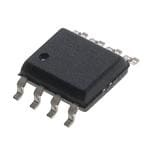
| 供应商器件封装 | 8-SOIC |
| 其它名称 | 296-1361-1 |
| 包装 | 剪切带 (CT) |
| 单位重量 | 76 mg |
| 商标 | Texas Instruments |
| 回动电压—最大值 | 12 mV at 0 A |
| 安装类型 | 表面贴装 |
| 安装风格 | SMD/SMT |
| 封装 | Reel |
| 封装/外壳 | 8-SOIC(0.154",3.90mm 宽) |
| 封装/箱体 | SOIC-8 |
| 工作温度 | -40°C ~ 125°C |
| 工厂包装数量 | 2500 |
| 最大功率耗散 | 0.725 W |
| 最大工作温度 | + 125 C |
| 最大输入电压 | 10 V |
| 最小工作温度 | - 40 C |
| 最小输入电压 | + 5.41 V |
| 标准包装 | 1 |
| 电压-跌落(典型值) | 0.19V @ 250mA |
| 电压-输入 | 5.41 V ~ 10 V |
| 电压-输出 | 5V |
| 电压调节准确度 | 2 % |
| 电流-输出 | 250mA |
| 电流-限制(最小值) | - |
| 稳压器拓扑 | 正,固定式 |
| 稳压器数 | 1 |
| 系列 | TPS7250 |
| 线路调整率 | 28 mV |
| 负载调节 | 79 mV |
| 输入偏压电流—最大 | 0.18 mA |
| 输出电压 | 5 V |
| 输出电流 | 250 mA |
| 输出端数量 | 1 Output |
| 输出类型 | Fixed |


- 商务部:美国ITC正式对集成电路等产品启动337调查
- 曝三星4nm工艺存在良率问题 高通将骁龙8 Gen1或转产台积电
- 太阳诱电将投资9.5亿元在常州建新厂生产MLCC 预计2023年完工
- 英特尔发布欧洲新工厂建设计划 深化IDM 2.0 战略
- 台积电先进制程称霸业界 有大客户加持明年业绩稳了
- 达到5530亿美元!SIA预计今年全球半导体销售额将创下新高
- 英特尔拟将自动驾驶子公司Mobileye上市 估值或超500亿美元
- 三星加码芯片和SET,合并消费电子和移动部门,撤换高东真等 CEO
- 三星电子宣布重大人事变动 还合并消费电子和移动部门
- 海关总署:前11个月进口集成电路产品价值2.52万亿元 增长14.8%


PDF Datasheet 数据手册内容提取
TPS7201Q, TPS7225Q, TPS7230Q TPS7233Q, TPS7248Q, TPS7250Q, TPS72xxY MICROPOWER LOW-DROPOUT (LDO) VOLTAGE REGULATORS SLVS102G – MARCH 1995 – REVISED JUNE 2000 (cid:0) Available in 5-V, 4.85-V, 3.3-V, 3.0-V, and D, P, OR PW PACKAGE 2.5-V Fixed-Output and Adjustable Versions (TOP VIEW) (cid:0) Dropout Voltage <85 mV Max at SENSE†/FB‡ 1 8 OUT I = 100 mA (TPS7250) O RESET/PG 2 7 OUT (cid:0) Low Quiescent Current, Independent of GND 3 6 IN Load, 180 m A Typ EN 4 5 IN (cid:0) 8-Pin SOIC and 8-Pin TSSOP Package (cid:0) Output Regulated to ±2% Over Full †SENSE – Fixed voltage options only (TPS7225, TPS7230, TPS7233, TPS7248, Operating Range for Fixed-Output Versions and TPS7250) (cid:0) Extremely Low Sleep-State Current, ‡FB – Adjustable version only (TPS7201) 0.5 m A Max (cid:0) Power-Good (PG) Status Output 600 TA = 25°C description 500 The TPS72xx family of low-dropout (LDO) voltage V regulators offers the benefits of low-dropout m TPS7225 voltage, micropower operation, and miniaturized ge – 400 TPS7230 packaging. These regulators feature extremely olta low dropout voltages and quiescent currents V compared to conventional LDO regulators. out 300 TPS7233 p Offered in small-outline integrated-circuit (SOIC) o r packages and 8-terminal thin shrink small-outline – D 200 TPS7248 (TSSOP), the TPS72xx series devices are ideal O D for cost-sensitive designs and for designs where V 100 board space is at a premium. TPS7250 A combination of new circuit design and process innovation has enabled the usual pnp pass 0 0 50 100 150 200 250 transistor to be replaced by a PMOS device. IO – Output Current – mA Because the PMOS pass element behaves as a low-value resistor, the dropout voltage is very low Figure 1. Typical Dropout Voltage Versus – maximum of 85 mV at 100 mA of load current Output Current (TPS7250) – and is directly proportional to the load current (see Figure 1). Since the PMOS pass element is a voltage-driven device, the quiescent current is very low (300 m A maximum) and is stable over the entire range of output load current (0 mA to 250 mA). Intended for use in portable systems such as laptops and cellular phones, the low-dropout voltage and micropower operation result in a significant increase in system battery operating life. The TPS72xx also features a logic-enabled sleep mode to shut down the regulator, reducing quiescent current to 0.5 m A maximum at T = 25°C. Other features include a power-good function that reports low output voltage J and may be used to implement a power-on reset or a low-battery indicator. The TPS72xx is offered in 2.5-V, 3-V, 3.3-V, 4.85-V, and 5-V fixed-voltage versions and in an adjustable version (programmable over the range of 1.2 V to 9.75 V). Output voltage tolerance is specified as a maximum of 2% over line, load, and temperature ranges (3% for adjustable version). Please be aware that an important notice concerning availability, standard warranty, and use in critical applications of TexasInstruments semiconductor products and disclaimers thereto appears at the end of this data sheet. PRODUCTION DATA information is current as of publication date. Copyright 2000, Texas Instruments Incorporated Products conform to specifications per the terms of Texas Instruments standard warranty. Production processing does not necessarily include testing of all parameters. POST OFFICE BOX 655303 • DALLAS, TEXAS 75265 1
TPS7201Q, TPS7225Q, TPS7230Q TPS7233Q, TPS7248Q, TPS7250Q, TPS72xxY MICROPOWER LOW-DROPOUT (LDO) VOLTAGE REGULATORS SLVS102G – MARCH 1995 – REVISED JUNE 2000 AVAILABLE OPTIONS OUTPUT VOLTAGE PACKAGED DEVICES (V) CHIP FORM TTJJ SMALL OUTLINE PDIP TSSOP (Y) MIN TYP MAX (D) (P) (PW) 4.9 5 5.1 TPS7250QD TPS7250QP TPS7250QPWR TPS7250Y 4.75 4.85 4.95 TPS7248QD TPS7248QP TPS7248QPWR TPS7248Y 3.23 3.3 3.37 TPS7233QD TPS7233QP TPS7233QPWR TPS7233Y –55°C to 150°C 2.94 3 3.06 TPS7230QD TPS7230QP TPS7230QPWR TPS7230Y 2.45 2.5 2.55 TPS7225QD TPS7225QP TPS7225QPWR TPS7225Y Adjustable TPS7201QD TPS7201QP TPS7201QPWR TPS7201Y 1.2 V to 9.75 V The D package is available taped and reeled. Add R suffix to device type (e.g., TPS7250QDR). The PW package is only available left-end taped and reeled. The TPS7201Q is programmable using an external resistor divider (see application information). The chip form is tested at 25°C. TPS72xx‡ 5 2 VI IN PG PG 6 1 250 kW IN SENSE 7 OUT VO 0.1 m F 4 8 EN OUT CO (see Note A) GND + 10 m F 3 CSR = 1 W ‡TPS7225Q, TPS7230Q, TPS7233Q, TPS7248Q, TPS7250Q (fixed-voltage options) NOTE A: Capacitor selection is nontrivial. See application information section for details. Figure 2. Typical Application Configuration 2 POST OFFICE BOX 655303 • DALLAS, TEXAS 75265
TPS7201Q, TPS7225Q, TPS7230Q TPS7233Q, TPS7248Q, TPS7250Q, TPS72xxY MICROPOWER LOW-DROPOUT (LDO) VOLTAGE REGULATORS SLVS102G – MARCH 1995 – REVISED JUNE 2000 TPS72xx chip information These chips, when properly assembled, display characteristics similar to the TPS72xxQ. Thermal compression or ultrasonic bonding may be used on the doped aluminum bonding pads. The chips may be mounted with conductive epoxy or a gold-silicon preform. (5) BONDING PAD ASSIGNMENTS SENSE(cid:0) (3) (6) IN FB(cid:1) 7 (6)6 5(5) 4(4) EN (2) TPS72xx (4) OUT (7) PG (1) (7) GND CHIP THICKNESS: 15 MILS TYPICAL 57 BONDING PADS: 4 × 4 MILS MINIMUM TJmax = 150°C 1 TOLERANCES ARE ±10%. ALL DIMENSIONS ARE IN MILS. †Fixed-voltage options only (TPS7225, TPS7230, (1) (2) 2 3 (3) TPS7233, TPS7248, and TPS7250) ‡Adjustable version only (TPS7201) 69 NOTE A. For most applications, OUT and SENSE should be tied together as close as possible to the device; for other implementations, refer to the SENSE-pin connection discussion in the application information section of this data sheet. functional block diagram IN RESISTOR DIVIDER OPTIONS § DEVICE R1 R2 UNIT § § EN TPS7201 0 ∞ W TPS7225 257 233 kW PG TPS7230 357 233 kW _ TPS7233 420 233 kW TPS7248 726 233 kW + TPS7250 756 233 kW OUT 1.12 V SENSE¶/FB NOTE A: Resistors are nominal values only. + _ R1 Vref = 1.188 V COMPONENT COUNT MOS transistors 108 R2 Bilpolar transistors 41 Diodes 4 Capacitors 15 Resistors 75 GND §Switch positions are shown with EN low (active). ¶For most applications, SENSE should be externally connected to OUT as close as possible to the device. For other implementations, refer to the SENSE-pin connection discussion in application information section. POST OFFICE BOX 655303 • DALLAS, TEXAS 75265 3
TPS7201Q, TPS7225Q, TPS7230Q TPS7233Q, TPS7248Q, TPS7250Q, TPS72xxY MICROPOWER LOW-DROPOUT (LDO) VOLTAGE REGULATORS SLVS102G – MARCH 1995 – REVISED JUNE 2000 absolute maximum ratings over operating free-air temperature range (unless otherwise noted)(cid:0) Input voltage range(cid:0), V, PG, SENSE, EN . . . . . . . . . . . . . . . . . . . . . . . . . . . . . . . . . . . . . . . . . . . . –0.3 V to 11 V I Output current, I . . . . . . . . . . . . . . . . . . . . . . . . . . . . . . . . . . . . . . . . . . . . . . . . . . . . . . . . . . . . . . . . . . . . . . . . . 1.5 A O Continuous total power dissipation . . . . . . . . . . . . . . . . . . . . . . . . . . . . . See Dissipation Rating Tables 1 and 2 Operating virtual junction temperature range, T . . . . . . . . . . . . . . . . . . . . . . . . . . . . . . . . . . . . . –55°C to 150°C J Storage temperature range, T . . . . . . . . . . . . . . . . . . . . . . . . . . . . . . . . . . . . . . . . . . . . . . . . . . . –65°C to 150°C stg Lead temperature 1,6 mm (1/16 inch) from case for 10 seconds . . . . . . . . . . . . . . . . . . . . . . . . . . . . . . . 260°C †Stresses beyond those listed under “absolute maximum ratings” may cause permanent damage to the device. These are stress ratings only, and functional operation of the device at these or any other conditions beyond those indicated under “recommended operating conditions” is not implied. Exposure to absolute-maximum-rated conditions for extended periods may affect device reliability. ‡All voltage values are with respect to network ground terminal. DISSIPATION RATING TABLE 1 – FREE-AIR TEMPERATURE (see Note 1 and Figure 3) PPAACCKKAAGGEE TAA ≤ 25°C DERATING FACTOR TAA = 70°C TAA = 85°C TAA = 125°C POWER RATING ABOVE TA = 25°C POWER RATING POWER RATING POWER RATING D 725 mW 5.8 mW/°C 464 mW 377 mW 145 mW PP 11117755 mmWW 88.7744 mmWW//°°CC 778822 mmWW 665500 mmWW 330011 mmWW PW 525 mW 4.2 mW/°C 336 mW 273 mW 105 mW DISSIPATION RATING TABLE 2 – CASE TEMPERATURE (see Note 1 and Figure 4) PPAACCKKAAGGEE TCC ≤ 25°C DERATING FACTOR TCC = 70°C TCC = 85°C TCC = 125°C POWER RATING ABOVE TC = 25°C POWER RATING POWER RATING POWER RATING D 2063 mW 16.5 mW/°C 1320 mW 1073 mW 413 mW PP 22773388 mmWW 2200.4499 mmWW//°°CC 11881166 mmWW 11550088 mmWW 668899 mmWW PW 2900 mW 23.2 mW/°C 1856 mW 1508 mW 580 mW NOTE 1: Dissipation rating tables and figures are provided for maintenance of junction temperature at or below absolute maximum of 150°C. For guidelines on maintaining junction temperature within the recommended operating range, see application information section. MAXIMUM CONTINUOUS DISSIPATION MAXIMUM CONTINUOUS DISSIPATION vs vs FREE-AIR TEMPERATURE CASE TEMPERATURE 1200 3000 W 1100 W P Package m m Rq JC = 48.8°C/W on – 1000 PR qPJaAc k=a 1g1e4.4°C/W on – 2500 ati 900 ati p p ssi 800 ssi 2000 Di D Package Di PW Package us 700 Rq JA = 172°C/W us Rq JC = 43.1°C/W o o u 600 u 1500 n n nti 500 nti o o C C m 400 m 1000 mu 300 mu D Package axi PW Package axi Rq JC = 60.6°C/W – M 200 Rq JA = 238°C/W – M 500 D 100 D P P 0 0 25 50 75 100 125 150 25 50 75 100 125 150 TA – Free-Air Temperature – °C TC – Case Temperature – °C Figure 3 Figure 4 4 POST OFFICE BOX 655303 • DALLAS, TEXAS 75265
TPS7201Q, TPS7225Q, TPS7230Q TPS7233Q, TPS7248Q, TPS7250Q, TPS72xxY MICROPOWER LOW-DROPOUT (LDO) VOLTAGE REGULATORS SLVS102G – MARCH 1995 – REVISED JUNE 2000 recommended operating conditions MIN MAX UNIT TPS7201Q 3 10 TPS7225Q 3.65 10 TPS7230Q 3.96 10 IInnppuutt vvoollttaaggee, VVII†††† VV TPS7233Q 3.98 10 TPS7248Q 5.24 10 TPS7250Q 5.41 10 High-level input voltage at EN, VIH 2 V Low-level input voltage at EN, VIL 0.5 V Output current, IO 0 250 mA Operating virtual junction temperature, TJ –40 125 °C †Minimum input voltage defined in the recommended operating conditions is the maximum specified output voltage plus dropout voltage at the maximum specified load range. Since dropout voltage is a function of output current, the usable range can be extended for lighter loads. To calculate the minimum input voltage for the maximum load current used in a given application, use the following equation: V (cid:1)V (cid:0)V I(min) O(max) DO(maxload) Because the TPS7201 is programmable, rDS(on) should be used to calculate VDO before applying the above equation. The equation for calculating VDO from rDS(on) is given in Note 3 under the TPS7201 electrical characteristics table. The minimum value of 3 V is the absolute lower limit for the recommended input-voltage range for the TPS7201. POST OFFICE BOX 655303 • DALLAS, TEXAS 75265 5
TPS7201Q, TPS7225Q, TPS7230Q TPS7233Q, TPS7248Q, TPS7250Q, TPS72xxY MICROPOWER LOW-DROPOUT (LDO) VOLTAGE REGULATORS SLVS102G – MARCH 1995 – REVISED JUNE 2000 electrical characteristics, I = 10 mA, EN = 0 V, C = 4.7 m F (CSR† = 1 W ), SENSE/FB shorted to OUT O O (unless otherwise noted) TPS72xxQ PPAARRAAMMEETTEERR TTEESSTT CCOONNDDIITTIIOONNSS‡‡ TTJJ UUNNIITT MIN TYP MAX GGrroouunndd ccuurrrreenntt ((aaccttiivvee mmooddee)) EENN ≤≤ 00..55 VV,, VVII = VVOO ++ 11 VV,, 25°C 180 225 mm AA 0 mA ≤ IO ≤ 250 mA –40°C to 125°C 325 25°C 0.5 IInnppuutt ccuurrrreenntt ((ssttaannddbbyy mmooddee)) EENN = VVI, 33 VV ≤≤ VVI ≤≤ 1100 VV –40°C to 125°C 1 mm AA 25°C 0.6 1 OOuuttppuutt ccuurrrreenntt lliimmiitt tthhrreesshhoolldd VVOO == 00 VV VVII == 1100 VV AA –40°C to 125°C 1.5 Pass-element leakagge current in 25°C 0.5 standby mode EENN = VVII, 33 VV ≤≤ VVII ≤≤ 1100 VV –40°C to 125°C 1 mm AA 25°C 0.5 PPGG lleeaakkaaggee ccuurrrreenntt VVPPGG == 1100 VV, NNoorrmmaall ooppeerraattiioonn mm AA –40°C to 125°C 0.5 Output voltage temperature coefficient –40°C to 125°C 31 75 ppm/°C Thermal shutdown junction temperature 165 °C 3 V ≤ VI ≤ 6 V 2 EENN llooggiicc hhiigghh ((ssttaannddbbyy mmooddee)) –4400°°CC ttoo 112255°°CC VV 6 V ≤ VI ≤ 10 V 2.7 25°C 0.5 EENN llooggiicc llooww ((aaccttiivvee mmooddee)) 33 VV ≤≤ VVII ≤≤ 1100 VV VV –40°C to 125°C 0.5 EN hysteresis voltage 25°C 50 mV 25°C –0.5 0.5 EENN iinnppuutt ccuurrrreenntt 00 VV ≤≤ VVII ≤≤ 1100 VV mm AA –40°C to 125°C –0.5 0.5 25°C 1.9 2.5 MMiinniimmuumm VVII ffoorr aaccttiivvee ppaassss eelleemmeenntt VV –40°C to 125°C 2.5 25°C 1.1 1.5 MMiinniimmuumm VVII ffoorr vvaalliidd PPGG IIPPGG == 330000 mm AA –40°C to 125°C 1.9 VV †CSR(compensation series resistance) refers to the total series resistance, including the equivalent series resistance (ESR) of the capacitor, any series resistance added externally, and PWB trace resistance to CO. ‡Pulse-testing techniques are used to maintain virtual junction temperature as close as possible to ambient temperature; thermal effects must be taken into account separately. 6 POST OFFICE BOX 655303 • DALLAS, TEXAS 75265
TPS7201Q, TPS7225Q, TPS7230Q TPS7233Q, TPS7248Q, TPS7250Q, TPS72xxY MICROPOWER LOW-DROPOUT (LDO) VOLTAGE REGULATORS SLVS102G – MARCH 1995 – REVISED JUNE 2000 TPS7201Q electrical characteristics, IO = 10 mA, VI = 3.5 V, EN = 0 V, CO = 4.7 m F (CSR† = 1 W ), FB shorted to OUT at device leads (unless otherwise noted) TPS7201Q PPAARRAAMMEETTEERR TTEESSTT CCOONNDDIITTIIOONNSS‡‡ TTJJ UUNNIITT MIN TYP MAX Reference voltagge ((measured VI = 3.5 V, IO = 10 mA 25°C 1.188 V at FB with OUT connected to 3 V ≤ VI ≤ 10 V, 5 mA ≤ IO ≤ 250 mA, –40°C to 125°C 1.152 1.224 V FB) See Note 2 Reference voltage –40°C to 125°C 31 75 ppm/°C temperature coefficient VI = 2.4 V,§ 50 m A ≤ IO ≤ 100 mA 25°C 2.1 VI = 2.4 V,§ 100 mA ≤ IO ≤ 200 mA 25°C 2.9 Pass-element series VVII == 22.99 VV, 5500 mm AA ≤≤ IIOO ≤≤ 225500 mmAA 25°C 1.6 2.7 WW resistance (see Note 3) –40°C to 125°C 4.5 VI = 3.9 V, 50 m A ≤ IO ≤ 250 mA 25°C 1 VI = 5.9 V, 50 m A ≤ IO ≤ 250 mA 25°C 0.8 IInnppuutt rreegguullaattiioonn VII = 3 V to 10 V,, 50 mm A ≤ IOO ≤ 250 mA,, 25°C 23 mmVV See Note 2 –40°C to 125°C 36 IOO = 5 mA to 250 mA,, 3 V ≤ VII ≤ 10 V,, 25°C 15 25 See Note 2 –40°C to 125°C 36 OOuuttppuutt rreegguullaattiioonn mmVV IOO = 50 mm A to 250 mA,, 3 V ≤ VII ≤ 10 V,, 25°C 17 27 See Note 2 –40°C to 125°C 43 25°C 49 60 IIOO == 5500 mm AA –40°C to 125°C 32 RRiippppllee rreejjeeccttiioonn ff == 112200 HHzz ddBB IOO = 250 mA,, 25°C 45 50 See Note 2 –40°C to 125°C 30 Output noise spectral density f = 120 Hz 25°C 2 m V/√Hz CO = 4.7 m F 25°C 235 1100 HHz ≤≤ ff ≤≤ 110000 kkHHz, Output noise voltage CCSSRR†† == 11 WW CO = 10 m F 25°C 190 m Vrms CO = 100 m F 25°C 125 0.95× PG trip-threshold voltage¶ VFB voltage decreasing from above VPG –40°C to 125°C VFB(nom) V PG hysteresis voltage¶ Measured at VFB 25°C 12 mV 25°C 0.1 0.4 PPGG oouuttppuutt llooww vvoollttaaggee¶¶ IIPPGG == 440000 mm AA, VVII == 22.1133 VV VV –40°C to 125°C 0.4 25°C –10 0.1 10 FFBB iinnppuutt ccuurrrreenntt nnAA –40°C to 125°C –20 20 †CSR refers to the total series resistance, including the ESR of the capacitor, any series resistance added externally, and PWB trace resistance to CO. ‡Pulse-testing techniques are used to maintain virtual junction temperature as close as possible to ambient temperature; thermal effects must be taken into account separately. §This voltage is not recommended. ¶Output voltage programmed to 2.5 V with closed-loop configuration (see application information). NOTES: 2. When VI < 2.9 V and IO > 100 mA simultaneously, pass element rDS(on) increases (see Figure 10) to a point such that the resulting dropout voltage prevents the regulator from maintaining the specified tolerance range. 3. To calculate dropout voltage, use equation: VDO = IO ⋅ rDS(on) rDS(on) is a function of both output current and input voltage. The parametric table lists rDS(on) for VI = 2.4 V, 2.9 V, 3.9 V, and 5.9 V, which corresponds to dropout conditions for programmed output voltages of 2.5 V, 3 V, 4 V, and 6 V, respectively. For other programmed values, refer to Figures 10 and 11. POST OFFICE BOX 655303 • DALLAS, TEXAS 75265 7
TPS7201Q, TPS7225Q, TPS7230Q TPS7233Q, TPS7248Q, TPS7250Q, TPS72xxY MICROPOWER LOW-DROPOUT (LDO) VOLTAGE REGULATORS SLVS102G – MARCH 1995 – REVISED JUNE 2000 TPS7225Q electrical characteristics, IO = 10 mA, VI = 3.5 V, EN = 0 V, CO = 4.7 m F (CSR† = 1 W ), SENSE shorted to OUT (unless otherwise noted) TPS7225Q PPAARRAAMMEETTEERR TTEESSTT CCOONNDDIITTIIOONNSS‡‡ TTJJ UUNNIITT MIN TYP MAX VI = 3.5 V, IO = 10 mA 25°C 2.5 OOuuttppuutt vvoollttaaggee VV 3.5 V ≤ VI ≤ 10 V, 5 mA ≤ IO ≤ 250 mA –40°C to 125°C 2.45 2.55 25°C 560 850 mV DDrrooppoouutt vvoollttaaggee IIOO == 225500 mmAA, VVII == 22.9977 VV –40°C to 125°C 1.1 V PPaassss-eelleemmeenntt sseerriieess rreessiissttaannccee ((2.97 V – VOO))/IOO,, VII = 2.97 V,, 25°C 2.24 3.4 WW IO = 250 mA –40°C to 125°C 3.84 25°C 9 27 IInnppuutt rreegguullaattiioonn VVII == 33.55 VV ttoo 1100 VV, 5500 mm AA ≤≤ IIOO ≤≤ 225500 mmAA mmVV –40°C to 125°C 33 25°C 28 36 IIOO == 55 mmAA ttoo 225500 mmAA, 33.55 VV ≤≤ VVII ≤≤ 1100 VV –40°C to 125°C 60 OOuuttppuutt rreegguullaattiioonn mmVV 25°C 24 41 IIOO == 5500 mm AA ttoo 225500 mmAA, 33.55 VV ≤≤ VVII ≤≤ 1100 VV –40°C to 125°C 73 25°C 47 58 IIOO == 5500 mm AA –40°C to 125°C 45 RRiippppllee rreejjeeccttiioonn ff == 112200 HHzz ddBB 25°C 40 46 IIOO == 225500 mmAA –40°C to 125°C 38 Output noise spectral density f = 120 Hz 25°C 2 m V/√Hz CO = 4.7 m F 25°C 248 1100 HHz ≤≤ ff ≤≤ 110000 kkHHz, Output noise voltage CCSSRR†† == 11 WW CO = 10 m F 25°C 200 m Vrms CO = 100 m F 25°C 130 0.95× PG trip-threshold voltage VO voltage decreasing from above VPG –40°C to 125°C VO(nom) V PG hysteresis voltage 25°C 50 mV 25°C 0.3 0.44 PPGG oouuttppuutt llooww vvoollttaaggee IIPPGG == 11.22 mmAA, VVII == 22.1133 VV –40°C to 125°C 0.5 VV †CSR refers to the total series resistance, including the ESR of the capacitor, any series resistance added externally, and PWB trace resistance to CO. ‡Pulse-testing techniques are used to maintain virtual junction temperature as close as possible to ambient temperature; thermal effects must be taken into account separately. 8 POST OFFICE BOX 655303 • DALLAS, TEXAS 75265
TPS7201Q, TPS7225Q, TPS7230Q TPS7233Q, TPS7248Q, TPS7250Q, TPS72xxY MICROPOWER LOW-DROPOUT (LDO) VOLTAGE REGULATORS SLVS102G – MARCH 1995 – REVISED JUNE 2000 TPS7230Q electrical characteristics, IO = 10 mA, VI = 4 V, EN = 0 V, CO = 4.7 m F (CSR† = 1 W ), SENSE shorted to OUT (unless otherwise noted) TPS7230Q PPAARRAAMMEETTEERR TTEESSTT CCOONNDDIITTIIOONNSS‡‡ TTJJ UUNNIITT MIN TYP MAX VI = 4 V, IO = 10 mA 25°C 3 OOuuttppuutt vvoollttaaggee VV 4 V≤VI ≤ 10 V, 5 mA ≤ IO ≤ 250 mA –40°C to 125°C 2.94 3.06 25°C 145 185 IIOO == 110000 mmAA, VVII == 22.9977 VV –40°C to 125°C 270 DDrrooppoouutt vvoollttaaggee mmVV 25°C 390 502 IIOO == 225500 mmAA, VVII == 22.9977 VV –40°C to 125°C 900 PPaassss-eelleemmeenntt sseerriieess rreessiissttaannccee ((2.97 V – VOO))/IOO,, VII = 2.97 V,, 25°C 1.56 2.01 WW IO = 250 mA –40°C to 125°C 3.6 25°C 9 27 IInnppuutt rreegguullaattiioonn VVII == 44 VV ttoo 1100 VV, 5500 mm AA ≤≤ IIOO ≤≤ 225500 mmAA mmVV –40°C to 125°C 33 25°C 34 45 IIOO == 55 mmAA ttoo 225500 mmAA, 44 VV ≤≤ VVII ≤≤ 1100 VV –40°C to 125°C 74 OOuuttppuutt rreegguullaattiioonn mmVV 25°C 42 60 IIOO == 5500 mm AA ttoo 225500 mmAA, 44 VV ≤≤ VVII ≤≤ 1100 VV –40°C to 125°C 98 25°C 45 56 IIOO == 5500 mm AA –40°C to 125°C 44 RRiippppllee rreejjeeccttiioonn ff == 112200 HHzz ddBB 25°C 40 45 IIOO == 225500 mmAA –40°C to 125°C 38 Output noise spectral density f = 120 Hz 25°C 2 m V/√Hz CO = 4.7 m F 25°C 256 1100 HHz ≤≤ ff ≤≤ 110000 kkHHz, Output noise voltage CCSSRR†† == 11 WW CO = 10 m F 25°C 206 m Vrms CO = 100 m F 25°C 132 0.95 × PG trip-threshold voltage VO voltage decreasing from above VPG –40°C to 125°C VO(nom) V PG hysteresis voltage 25°C 50 mV 25°C 0.25 0.44 PPGG oouuttppuutt llooww vvoollttaaggee IIPPGG == 11.22 mmAA, VVII == 22.5555 VV –40°C to 125°C 0.44 VV †CSR refers to the total series resistance, including the ESR of the capacitor, any series resistance added externally, and PWB trace resistance to CO. ‡Pulse-testing techniques are used to maintain virtual junction temperature as close as possible to ambient temperature; thermal effects must be taken into account separately. POST OFFICE BOX 655303 • DALLAS, TEXAS 75265 9
TPS7201Q, TPS7225Q, TPS7230Q TPS7233Q, TPS7248Q, TPS7250Q, TPS72xxY MICROPOWER LOW-DROPOUT (LDO) VOLTAGE REGULATORS SLVS102G – MARCH 1995 – REVISED JUNE 2000 TPS7233Q electrical characteristics, IO = 10 mA, VI = 4.3 V, EN = 0 V, CO = 4.7 m F (CSR† = 1 W ), SENSE shorted to OUT (unless otherwise noted) TPS7233Q PPAARRAAMMEETTEERR TTEESSTT CCOONNDDIITTIIOONNSS‡‡ TTJJ UUNNIITT MIN TYP MAX VI = 4.3 V, IO = 10 mA 25°C 3.3 OOuuttppuutt vvoollttaaggee VV 4.3 V ≤ VI ≤ 10 V, 5 mA ≤ IO ≤ 250 mA –40°C to 125°C 3.23 3.37 25°C 14 20 IIOO == 1100 mmAA, VVII == 33.2233 VV –40°C to 125°C 30 25°C 140 180 DDrrooppoouutt vvoollttaaggee IIOO == 110000 mmAA, VVII == 33.2233 VV mmVV –40°C to 125°C 232 25°C 360 460 IIOO == 225500 mmAA, VVII == 33.2233 VV –40°C to 125°C 610 PPaassss-eelleemmeenntt sseerriieess rreessiissttaannccee ((3.23 V – VOO))/IOO,, VII = 3.23 V,, 25°C 1.5 1.84 WW IO = 250 mA –40°C to 125°C 2.5 25°C 8 25 IInnppuutt rreegguullaattiioonn VVII == 44.33 VV ttoo 1100 VV, 5500 mm AA ≤≤ IIOO ≤≤ 225500 mmAA mmVV –40°C to 125°C 33 25°C 32 42 IIOO == 55 mmAA ttoo 225500 mmAA, 44.33 VV ≤≤ VVII ≤≤ 1100 VV –40°C to 125°C 71 OOuuttppuutt rreegguullaattiioonn mmVV 25°C 41 55 IIOO == 5500 mm AA ttoo 225500 mmAA, 44.33 VV ≤≤ VVII ≤≤ 1100 VV –40°C to 125°C 98 25°C 40 52 IIOO == 5500 mm AA –40°C to 125°C 38 RRiippppllee rreejjeeccttiioonn ff == 112200 HHzz ddBB 25°C 35 44 IIOO == 225500 mmAA –40°C to 125°C 33 Output noise spectral density f = 120 Hz 25°C 2 m V/√Hz CO = 4.7 m F 25°C 265 1100 HHz ≤≤ ff ≤≤ 110000 kkHHz, Output noise voltage CCSSRR†† == 11 WW CO = 10 m F 25°C 212 m Vrms CO = 100 m F 25°C 135 0.95× PG trip-threshold voltage VO voltage decreasing from above VPG –40°C to 125°C VO(nom) V PG hysteresis voltage 25°C 32 mV 25°C 0.22 0.4 PPGG oouuttppuutt llooww vvoollttaaggee IIPPGG == 11.22 mmAA, VVII == 22.88 VV –40°C to 125°C 0.4 VV †CSR refers to the total series resistance, including the ESR of the capacitor, any series resistance added externally, and PWB trace resistance to CO. ‡Pulse-testing techniques are used to maintain virtual junction temperature as close as possible to ambient temperature; thermal effects must be taken into account separately. 10 POST OFFICE BOX 655303 • DALLAS, TEXAS 75265
TPS7201Q, TPS7225Q, TPS7230Q TPS7233Q, TPS7248Q, TPS7250Q, TPS72xxY MICROPOWER LOW-DROPOUT (LDO) VOLTAGE REGULATORS SLVS102G – MARCH 1995 – REVISED JUNE 2000 TPS7248Q electrical characteristics, IO = 10 mA, VI = 5.85 V, EN = 0 V, CO = 4.7 m F (CSR† = 1 W ), SENSE shorted to OUT (unless otherwise noted) TPS7248Q PPAARRAAMMEETTEERR TTEESSTT CCOONNDDIITTIIOONNSS‡‡ TTJJ UUNNIITT MIN TYP MAX VI = 5.85 V, IO = 10 mA 25°C 4.85 OOuuttppuutt vvoollttaaggee VV 5.85 V≤VI ≤ 10 V, 5 mA ≤ IO ≤ 250 mA –40°C to 125°C 4.75 4.95 25°C 10 19 IIOO == 1100 mmAA, VVII == 44.7755 VV –40°C to 125°C 30 25°C 90 100 DDrrooppoouutt vvoollttaaggee IIOO == 110000 mmAA, VVII == 44.7755 VV mmVV –40°C to 125°C 150 25°C 216 250 IIOO == 225500 mmAA, VVII == 44.7755 VV –40°C to 125°C 285 PPaassss-eelleemmeenntt sseerriieess rreessiissttaannccee ((4.75 V – VOO))/IOO,, VII = 4.75 V,, 25°C 0.8 1 WW IO = 250 mA –40°C to 125°C 1.4 25°C 34 IInnppuutt rreegguullaattiioonn VVII == 55.8855 VV ttoo 1100 VV, 5500 mm AA ≤≤ IIOO ≤≤ 225500 mmAA mmVV –40°C to 125°C 50 25°C 43 55 IIOO == 55 mmAA ttoo 225500 mmAA, 55.8855 VV ≤≤ VVII ≤≤ 1100 VV –40°C to 125°C 95 OOuuttppuutt rreegguullaattiioonn mmVV 25°C 55 75 IIOO == 5500 mm AA ttoo 225500 mmAA, 55.8855 VV ≤≤ VVII ≤≤ 1100 VV –40°C to 125°C 135 25°C 42 53 IIOO == 5500 mm AA –40°C to 125°C 36 RRiippppllee rreejjeeccttiioonn ff == 112200 HHzz ddBB 25°C 36 46 IIOO == 225500 mmAA –40°C to 125°C 34 Output noise spectral density f = 120 Hz 25°C 2 m V/√Hz CO = 4.7 m F 25°C 370 1100 HHz ≤≤ ff ≤≤ 110000 kkHHz, Output noise voltage CCSSRR†† == 11 WW CO = 10 m F 25°C 290 m Vrms CO = 100 m F 25°C 168 0.95 × PG trip-threshold voltage VO voltage decreasing from above VPG –40°C to 125°C VO(nom) V PG hysteresis voltage 25°C 50 mV 25°C 0.2 0.4 PPGG oouuttppuutt llooww vvoollttaaggee IIPPGG == 11.22 mmAA, VVII == 44.1122 VV –40°C to 125°C 0.4 VV †CSR refers to the total series resistance, including the ESR of the capacitor, any series resistance added externally, and PWB trace resistance to CO. ‡Pulse-testing techniques are used to maintain virtual junction temperature as close as possible to ambient temperature; thermal effects must be taken into account separately. POST OFFICE BOX 655303 • DALLAS, TEXAS 75265 11
TPS7201Q, TPS7225Q, TPS7230Q TPS7233Q, TPS7248Q, TPS7250Q, TPS72xxY MICROPOWER LOW-DROPOUT (LDO) VOLTAGE REGULATORS SLVS102G – MARCH 1995 – REVISED JUNE 2000 TPS7250Q electrical characteristics, IO = 10 mA, VI = 6 V, EN = 0 V, CO = 4.7 m F (CSR† = 1 W ), SENSE shorted to OUT (unless otherwise noted) TPS7250Q PPAARRAAMMEETTEERR TTEESSTT CCOONNDDIITTIIOONNSS‡‡ TTJJ UUNNIITT MIN TYP MAX VI = 6 V, IO = 10 mA 25°C 5 OOuuttppuutt vvoollttaaggee VV 6 V≤VI ≤ 10 V, 5 mA ≤ IO ≤ 250 mA –40°C to 125°C 4.9 5.1 25°C 8 12 IIOO == 1100 mmAA, VVII == 44.8888 VV –40°C to 125°C 30 25°C 76 85 DDrrooppoouutt vvoollttaaggee IIOO == 110000 mmAA, VVII == 44.8888 VV mmVV –40°C to 125°C 136 25°C 190 206 IIOO == 225500 mmAA, VVII == 44.8888 VV –40°C to 125°C 312 PPaassss-eelleemmeenntt sseerriieess rreessiissttaannccee ((4.88 V – VOO))/IOO,, VII = 4.88 V,, 25°C 0.76 0.825 WW IO = 250 mA –40°C to 125°C 1.25 25°C 28 IInnppuutt rreegguullaattiioonn VVII == 66 VV ttoo 1100 VV, 5500 mm AA ≤≤ IIOO ≤≤ 225500 mmAA mmVV –40°C to 125°C 35 25°C 46 61 IIOO == 55 mmAA ttoo 225500 mmAA, 66 VV ≤≤ VVII ≤≤ 1100 VV –40°C to 125°C 100 OOuuttppuutt rreegguullaattiioonn mmVV 25°C 59 79 IIOO == 5500 mm AA ttoo 225500 mmAA, 66 VV ≤≤ VVII ≤≤ 1100 VV –40°C to 125°C 150 25°C 41 52 IIOO == 5500 mm AA –40°C to 125°C 37 RRiippppllee rreejjeeccttiioonn ff == 112200 HHzz ddBB 25°C 36 46 IIOO == 225500 mmAA –40°C to 125°C 32 Output noise spectral density f = 120 Hz 25°C 2 m V/√Hz CO = 4.7 m F 25°C 390 1100 HHz ≤≤ ff ≤≤ 110000 kkHHz, Output noise voltage CCSSRR†† == 11 WW CO = 10 m F 25°C 300 m Vrms CO = 100 m F 25°C 175 0.95 × PG trip-threshold voltage VO voltage decreasing from above VPG –40°C to 125°C VO(nom) V PG hysteresis voltage 25°C 50 mV 25°C 0.19 0.4 PPGG oouuttppuutt llooww vvoollttaaggee IIPPGG == 11.22 mmAA, VVII == 44.2255 VV –40°C to 125°C 0.4 VV †CSR refers to the total series resistance, including the ESR of the capacitor, any series resistance added externally, and PWB trace resistance to CO. ‡Pulse-testing techniques are used to maintain virtual junction temperature as close as possible to ambient temperature; thermal effects must be taken into account separately. 12 POST OFFICE BOX 655303 • DALLAS, TEXAS 75265
TPS7201Q, TPS7225Q, TPS7230Q TPS7233Q, TPS7248Q, TPS7250Q, TPS72xxY MICROPOWER LOW-DROPOUT (LDO) VOLTAGE REGULATORS SLVS102G – MARCH 1995 – REVISED JUNE 2000 electrical characteristics, I = 10 mA, EN = 0 V, C = 4.7 m F (CSR† = 1 W ), T = 25°C, SENSE/FB O O J shorted to OUT (unless otherwise noted) TPS72xxY PPAARRAAMMEETTEERR TTEESSTT CCOONNDDIITTIIOONNSS‡‡ UUNNIITT MIN TYP MAX Ground current (active mode) EN ≤ 0.5 V, VI = VO + 1 V, 180 m A 0 mA ≤ IO ≤ 250 mA Output current limit threshold VO = 0 V, VI = 10 V 0.6 A Thermal shutdown junction temperature 165 °C EN hysteresis voltage 50 mV Minimum VI for active pass element 1.9 V Minimum VI for valid PG IPG = 300 m A 1.1 V electrical characteristics, I = 10 mA, EN = 0 V, C = 4.7 m F (CSR† = 1 W ), T = 25°C, FB shorted to O O J OUT at device leads (unless otherwise noted) TPS7201Y PPAARRAAMMEETTEERR TTEESSTT CCOONNDDIITTIIOONNSS‡‡ UUNNIITT MIN TYP MAX Reference voltage (measured at FB with OUT connected to FB) VI = 3.5 V, IO = 10 mA 1.188 V VI = 2.4 V,§ 50 m A ≤ IO ≤ 100 mA 2.1 VI = 2.4 V,§ 100 mA ≤ IO ≤ 200 mA 2.9 Pass-element series resistance (see Note 3) VI = 2.9 V, 50 m A ≤ IO ≤ 250 mA 1.6 W VI = 3.9 V, 50 m A ≤ IO ≤ 250 mA 1 VI = 5.9 V, 50 m A ≤ IO ≤ 250 mA 0.8 3 V ≤ VI ≤ 10 V, IO = 5 mA to 250 mA, 15 See Note 2 OOuuttppuutt rreegguullaattiioonn mmVV 3 V ≤ VI ≤ 10 V, IO = 50 m A to 250 mA, 17 See Note 2 IO = 50 m A 60 VVII == 33.55 VV, Ripple rejection f = 120 Hz IO = 250 mA, 50 dB See Note 2 Output noise spectral density VI = 3.5 V, f = 120 Hz 2 m V/√Hz VVII == 33..55 VV,, CO = 4.7 m F 235 Output noise voltage 10 Hz ≤ f ≤ 100 kHz, CO = 10 m F 190 m Vrms CSR†† = 1 W CO = 100 m F 125 PG hysteresis voltage¶ VI = 3.5 V, Measured at VFB 12 mV PG output low voltage¶ VI = 2.13 V, IPG = 400 m A 0.1 V FB input current VI = 3.5 V 0.1 nA †CSR refers to the total series resistance, including the ESR of the capacitor, any series resistance added externally, and PWB trace resistance to CO. ‡Pulse-testing techniques are used to maintain virtual junction temperature as close as possible to ambient temperature; thermal effects must be taken into account separately. §This voltage is not recommended. ¶Output voltage programmed to 2.5 V with closed-loop configuration (see application information). NOTES: 2 When VI < 2.9 V and IO > 100 mA simultaneously, pass element rDS(on) increases (see Figure 10) to a point such that the resulting dropout voltage prevents the regulator from maintaining the specified tolerance range. 3 To calculate dropout voltage, use equation: VDO = IO ⋅ rDS(on) rDS(on) is a function of both output current and input voltage. The parametric table lists rDS(on) for VI = 2.4 V, 2.9 V, 3.9 V, and 5.9 V, which corresponds to dropout conditions for programmed output voltages of 2.5 V, 3 V, 4 V, and 6 V, respectively. For other programmed values, refer to Figures 10 and 11. POST OFFICE BOX 655303 • DALLAS, TEXAS 75265 13
TPS7201Q, TPS7225Q, TPS7230Q TPS7233Q, TPS7248Q, TPS7250Q, TPS72xxY MICROPOWER LOW-DROPOUT (LDO) VOLTAGE REGULATORS SLVS102G – MARCH 1995 – REVISED JUNE 2000 electrical characteristics, I = 10 mA, EN = 0 V, C = 4.7 m F (CSR† = 1 W ), T = 25°C, FB shorted to O O J OUT at device leads (unless otherwise noted) TPS7225Y PPAARRAAMMEETTEERR TTEESSTT CCOONNDDIITTIIOONNSS‡‡ UUNNIITT MIN TYP MAX Output voltage VI = 3.5 V, IO = 10 mA 2.5 V Dropout voltage VI = 2.97 V, IO = 250 mA 560 mV Pass-element series resistance (2.97 V – VO)/IO, VI = 2.97 V, 2.24 W IO = 250 mA Input regulation VI = 3.5 V to 10 V, 50 m A ≤ IO ≤ 250 mA 9 mV 3.5 V ≤ VI ≤ 10 V IO = 5 mA to 250 mA 28 OOuuttppuutt rreegguullaattiioonn mmVV 3.5 V ≤ VI ≤ 10 V IO = 50 m A to 250 mA 24 RRiippppllee rreejjeeccttiioonn VII = 3.5 V,, IO = 50 m A 58 ddBB f = 120 Hz IO = 250 mA 46 Output noise spectral density VI = 3.5 V, f = 120 Hz 2 m V/√Hz VVII == 33..55 VV,, CO = 4.7 m F 248 Output noise voltage 10 Hz ≤ f ≤ 100 kHz, CO = 10 m F 200 m Vrms CCSSRR†† = 1 W CO = 100 m F 130 PG hysteresis voltage VI = 3.5 V 50 mV PG output low voltage VI = 2.13 V IPG = 1.2 mA 0.3 V †CSR refers to the total series resistance, including the ESR of the capacitor, any series resistance added externally, and PWB trace resistance to CO. ‡Pulse-testing techniques are used to maintain virtual junction temperature as close as possible to ambient temperature; thermal effects must be taken into account separately. 14 POST OFFICE BOX 655303 • DALLAS, TEXAS 75265
TPS7201Q, TPS7225Q, TPS7230Q TPS7233Q, TPS7248Q, TPS7250Q, TPS72xxY MICROPOWER LOW-DROPOUT (LDO) VOLTAGE REGULATORS SLVS102G – MARCH 1995 – REVISED JUNE 2000 electrical characteristics, I = 10 mA, EN = 0 V, C = 4.7 m F (CSR† = 1 W ), T = 25°C, SENSE shorted O O J to OUT (unless otherwise noted) TPS7230Y PPAARRAAMMEETTEERR TTEESSTT CCOONNDDIITTIIOONNSS‡‡ UUNNIITT MIN TYP MAX Output voltage VI = 4 V, IO = 10 mA 3 V VI = 2.97 V, IO = 100 mA 145 DDrrooppoouutt vvoollttaaggee mmVV VI = 2.97 V, IO = 250 mA 390 Pass-element series resistance (2.97 V – VO)/IO, VI = 2.97 V, 1.56 W IO = 250 mA Input regulation VI = 4 V to 10 V, 50 m A ≤ IO ≤ 250 mA 9 mV 4 V ≤ VI ≤ 10 V IO = 5 mA to 250 mA 34 OOuuttppuutt rreegguullaattiioonn mmVV 4 V ≤ VI ≤ 10 V IO = 50 m A to 250 mA 41 RRiippppllee rreejjeeccttiioonn VII = 4 V,, IO = 50 m A 56 ddBB f = 120 Hz IO = 250 mA 45 Output noise spectral density VI = 4 V, f = 120 Hz 2 m V/√Hz VVII == 44 VV,, CO = 4.7 m F 256 Output noise voltage 10 Hz ≤ f ≤ 100 kHz, CO = 10 m F 206 m Vrms CCSSRR†† = 1 W CO = 100 m F 132 PG hysteresis voltage VI = 4 V 50 mV PG output low voltage VI = 2.55 V IPG = 1.2 mA 0.25 V †CSR refers to the total series resistance, including the ESR of the capacitor, any series resistance added externally, and PWB trace resistance to CO. ‡Pulse-testing techniques are used to maintain virtual junction temperature as close as possible to ambient temperature; thermal effects must be taken into account separately. TPS7233Y PPAARRAAMMEETTEERR TTEESSTT CCOONNDDIITTIIOONNSS‡‡ UUNNIITT MIN TYP MAX Output voltage VI = 4.3 V, IO = 10 mA 3.3 V VI = 3.23 V, IO = 10 mA 14 Dropout voltage VI = 3.23 V, IO = 100 mA 140 mV VI = 3.23 V, IO = 250 mA 360 Pass-element series resistance (3.23 V – VO)/IO, VI = 3.23 V, 1.5 W IO = 250 mA Input regulation VI = 4.3 V to 10 V, 50 m A ≤ IO ≤ 250 mA 8 mV 4.3 V ≤ VI ≤ 10 V, IO = 5 mA to 250 mA 32 OOuuttppuutt rreegguullaattiioonn mmVV 4.3 V ≤ VI ≤ 10 V, IO = 50 m A to 250 mA 41 RRiippppllee rreejjeeccttiioonn VII = 4.3 V,, IO = 50 m A 52 ddBB f = 120 Hz IO = 250 mA 44 Output noise spectral density VI = 4.3 V, f = 120 Hz 2 m V/√Hz VVII == 44..33 VV,, CO = 4.7 m F 265 Output noise voltage 10 Hz ≤ f ≤ 100 kHz, CO = 10 m F 212 m Vrms CCSSRR†† = 1 W CO = 100 m F 135 PG hysteresis voltage VI = 4.3 V 32 mV PG output low voltage VI = 2.8 V, IPG = 1.2 mA 0.22 V †CSR refers to the total series resistance, including the ESR of the capacitor, any series resistance added externally, and PWB trace resistance to CO. ‡Pulse-testing techniques are used to maintain virtual junction temperature as close as possible to ambient temperature; thermal effects must be taken into account separately. POST OFFICE BOX 655303 • DALLAS, TEXAS 75265 15
TPS7201Q, TPS7225Q, TPS7230Q TPS7233Q, TPS7248Q, TPS7250Q, TPS72xxY MICROPOWER LOW-DROPOUT (LDO) VOLTAGE REGULATORS SLVS102G – MARCH 1995 – REVISED JUNE 2000 electrical characteristics, I = 10 mA, EN = 0 V, C = 4.7 m F (CSR† = 1 W ), T = 25°C, SENSE shorted O O J to OUT (unless otherwise noted) (continued) TPS7248Y PPAARRAAMMEETTEERR TTEESSTT CCOONNDDIITTIIOONNSS‡‡ UUNNIITT MIN TYP MAX Output voltage VI = 5.85 V, IO = 10 mA 4.85 V VI = 4.75 V, IO = 10 mA 10 Dropout voltage VI = 4.75 V, IO = 100 mA 90 mV VI = 4.75 V, IO = 250 mA 216 Pass-element series resistance (4.75 V – VO)/IO, VI = 4.75 V, 0.8 W IO = 250 mA 5.85 V ≤ VI ≤ 10 V IO = 5 mA to 250 mA 43 OOuuttppuutt rreegguullaattiioonn mmVV 5.85 V ≤ VI ≤ 10 V IO = 50 m A to 250 mA 55 RRiippppllee rreejjeeccttiioonn VII = 5.85 V,, IO = 50 m A 53 ddBB f = 120 Hz IO = 250 mA 46 Output noise spectral density VI = 5.85 V, f = 120 Hz 2 m V/√Hz VVII == 55..8855 VV,, CO = 4.7 m F 370 Output noise voltage 10 Hz ≤ f ≤ 100 kHz, CO = 10 m F 290 m Vrms CCSSRR†† = 1 W CO = 100 m F 168 PG hysteresis voltage VI = 5.85 V 50 mV PG output low voltage VI = 4.12 V IPG = 1.2 mA 0.2 V †CSR refers to the total series resistance, including the ESR of the capacitor, any series resistance added externally, and PWB trace resistance to CO. ‡Pulse-testing techniques are used to maintain virtual junction temperature as close as possible to ambient temperature; thermal effects must be taken into account separately. TPS7250Y PPAARRAAMMEETTEERR TTEESSTT CCOONNDDIITTIIOONNSS‡‡ UUNNIITT MIN TYP MAX Output voltage VI = 6 V, IO = 10 mA 5 V VI = 4.88 V IO = 10 mA 8 Dropout voltage VI = 4.88 V IO = 100 mA 76 mV VI = 4.88 V, IO = 250 mA 190 Pass-element series resistance (4.88 V – VO)/IO, VI = 4.88 V, 0.76 W IO = 250 mA Input regulation VI = 6 V to 10 V, 50 m A ≤ IO ≤ 250 mA mV 6 V ≤ VI ≤ 10 V, IO = 5 mA to 250 mA 46 OOuuttppuutt rreegguullaattiioonn mmVV 6 V ≤ VI ≤ 10 V, IO = 50 m A to 250 mA 59 RRiippppllee rreejjeeccttiioonn VII = 6 V,, IO = 50 m A 52 ddBB f = 120 Hz IO = 250 mA 46 Output noise spectral density VI = 6 V, f = 120 Hz 2 m V/√Hz VVII == 66 VV,, CO = 4.7 m F 390 Output noise voltage 10 Hz ≤ f ≤ 100 kHz, CO = 10 m F 300 m Vrms CCSSRR†† = 1 W CO = 100 m F 175 PG hysteresis voltage VI = 6 V 50 mV PG output low voltage VI = 4.25 V, IPG = 1.2 mA 0.19 V †CSR refers to the total series resistance, including the ESR of the capacitor, any series resistance added externally, and PWB trace resistance to CO. ‡Pulse-testing techniques are used to maintain virtual junction temperature as close as possible to ambient temperature; thermal effects must be taken into account separately. 16 POST OFFICE BOX 655303 • DALLAS, TEXAS 75265
TPS7201Q, TPS7225Q, TPS7230Q TPS7233Q, TPS7248Q, TPS7250Q, TPS72xxY MICROPOWER LOW-DROPOUT (LDO) VOLTAGE REGULATORS SLVS102G – MARCH 1995 – REVISED JUNE 2000 TYPICAL CHARACTERISTICS Table of Graphs FIGURE vs Output current 5 IIQQ QQuuiieesscceenntt ccuurrrreenntt vs Input voltage 6 D IQ† Change in quiescent current vs Free-air temperature 7 VDO Dropout voltage vs Output current 8 D VDO Change in dropout voltage vs Free-air temperature 9 VDO Dropout voltage (TPS7201 only) vs Output current 10 rDS(on) Pass-element series resistance vs Input voltage 11 D VO Change in output voltage vs Free-air temperature 12 VO Output voltage vs Input voltage 13 Line regulation 14 (TPS7201, TPS7233, TPS7248, TPS7250) Load regulation 15 (TPS7225, TPS7233, TPS7248, TPS7250) VO(PG) Power-good (PG) voltage vs Output voltage 16 rDS(on)PG Power-good (PG) on-resistance vs Input voltage 17 VI Minimum input voltage for valid PG vs Free-air temperature 18 Output voltage response from enable (EN) 19 Load transient response (TPS7201/TPS7233) 20 Load transient response (TPS7248/TPS7250) 21 Line transient response (TPS7201) 22 Line transient response (TPS7233) 23 Line transient response (TPS7248/TPS7250) 24 Ripple rejection vs Frequency 25 Output Spectral Noise Density vs Frequency 26 vs Output current (CO = 4.7 m F) 27 vs Added ceramic capacitance (CO = 4.7 m F) 28 CCoommppeennssaattiioonn sseerriieess rreessiissttaannccee ((CCSSRR)) vs Output current (CO = 10 m F) 29 vs Added ceramic capacitance (CO = 10 m F) 30 †This symbol is not currently listed within EIA or JEDEC standards for semiconductor symbology. POST OFFICE BOX 655303 • DALLAS, TEXAS 75265 17
TPS7201Q, TPS7225Q, TPS7230Q TPS7233Q, TPS7248Q, TPS7250Q, TPS72xxY MICROPOWER LOW-DROPOUT (LDO) VOLTAGE REGULATORS SLVS102G – MARCH 1995 – REVISED JUNE 2000 TYPICAL CHARACTERISTICS QUIESCENT CURRENT QUIESCENT CURRENT vs vs OUTPUT CURRENT INPUT VOLTAGE 230 250 TA = 25°C TPS7248 VI = 10 V TA 25°C TPS7248 220 IO = 250 mA TPS7233 200 A 210 A mQuiescent Current – 112980000 TTTPPPSSS777222354308 VVVIII === 11500.8 VV5 V mQuiescent Current – 110500 TVPOS P7r2o0g1r aWmitmhed to 2.5 V – Q 170 – Q TPS7250 I TPS7250 VI = 6.0 V I 50 160 TPS7233 VI = 4.3 V 150 0 0 50 100 150 200 250 0 1 2 3 4 5 6 7 8 9 10 IO – Output Current – mA VI – Input Voltage – V Figure 5 Figure 6 CHANGE IN QUIESCENT CURRENT DROPOUT VOLTAGE vs vs FREE-AIR TEMPERATURE OUTPUT CURRENT 50 600 IO = 10 mA TA = 25°C A 40 VI = VO + 1 V 500 m– nt 30 V e m TPS7225 nt Curr 20 age – 400 TPS7230 ce 10 olt s V Quie 0 pout 300 TPS7233 n o e i Dr 200 TPS7248 g –10 – n a O h D C –20 V – 100 Q I –30 TPS7250 D – 40 0 – 40 – 20 0 20 40 60 80 100 120 140 0 50 100 150 200 250 TA – Free-Air Temperature – °C IO – Output Current – mA Figure 7 Figure 8 18 POST OFFICE BOX 655303 • DALLAS, TEXAS 75265
TPS7201Q, TPS7225Q, TPS7230Q TPS7233Q, TPS7248Q, TPS7250Q, TPS72xxY MICROPOWER LOW-DROPOUT (LDO) VOLTAGE REGULATORS SLVS102G – MARCH 1995 – REVISED JUNE 2000 TYPICAL CHARACTERISTICS TPS7201 CHANGE IN DROPOUT VOLTAGE DROPOUT VOLTAGE vs vs FREE-AIR TEMPERATURE OUTPUT CURRENT 0.05 1.6 V 0.04 TPS7230 1.4 VI = 2.4 V† – e g 0.03 TPS7233 1.2 olta – V VI = 2.9 V VI = 2.6 V† V 0.02 e opout 0.01 Voltag 1 VVII == 33..29 VV Dr TPS7248/TPS7250 ut 0.8 e in 0 opo VI = 5.9 V g r 0.6 n D ha –0.01 – VI = 9.65 V C O – O –0.02 VD 0.4 D V 0.2 D –0.03 –0.04 0 –40 –20 0 20 40 60 80 100 120 140 0 50 100 150 200 250 TA – Free-Air Temperature – °C IO – Output Current – mA †This voltage is not recommended. Figure 9 Figure 10 PASS ELEMENT SERIES RESISTANCE CHANGE IN OUTPUT VOLTAGE vs vs INPUT VOLTAGE FREE-AIR TEMPERATURE 6 15 Wnce – 5 TVAF B= =2 51°.C12 V mV 10 IVOI == V10O m+ A1 V es Resista 4 Voltage – 50 Seri IO = 250 mA put ent 3 Out –5 m n Ele ge i –10 s 2 n s a a h – P – C –15 on) 1 VO S( IO = 100 mA D –20 D r 0 –25 2 3 4 5 6 7 8 9 10 –40 –20 0 20 40 60 80 100 120 140 VI – Input Voltage – V TA – Free-Air Temperature – °C Figure 11 Figure 12 POST OFFICE BOX 655303 • DALLAS, TEXAS 75265 19
TPS7201Q, TPS7225Q, TPS7230Q TPS7233Q, TPS7248Q, TPS7250Q, TPS72xxY MICROPOWER LOW-DROPOUT (LDO) VOLTAGE REGULATORS SLVS102G – MARCH 1995 – REVISED JUNE 2000 TYPICAL CHARACTERISTICS OUTPUT VOLTAGE vs INPUT VOLTAGE LINE REGULATION 5.5 25 TA = 25°C TPS7250 TA = 25°C 5 IO = 250 mA V 20 IO = 250 mA 4.5 TPS7248 m – 15 V 4 ge TPS7201 With ge – 3.5 Volta 10 VO Programmed to 2.5 V olta 3 TPS7233 put 5 TPS7233 ut V Out 0 p 2.5 n Out 2 ge i –5 – n TPS7248 VO 1.5 TVPOS P7r2o0g1r aWmitmhed to 2.5 V Cha –10 – D 1 O –15 V TPS7250 0.5 D –20 0 –25 0 1 2 3 4 5 6 7 8 9 10 4 4.5 5 5.5 6 6.5 7 7.5 8 8.5 9 9.5 10 VI – Input Voltage – V VI – Input Voltage – V Figure 13 Figure 14 POWER-GOOD (PG) VOLTAGE vs LOAD REGULATION OUTPUT VOLTAGE† 50 6 TA = 25°C TA = 25°C 40 PG Pulled Up to VI With 5 k W Resistor – mV 30 e – V VI oltage 20 Voltag ut V 10 PG) Outp 0 TPS7233 ood ( n G ge i –10 wer- han –20 TPS7225 Po C TPS7248 – – –30 ÁG)Á O P GND V TPS7250 ÁO(Á D –40 V –50 0 92 93 94 95 96 97 98 0 50 100 150 200 250 IO – Output Current – mA VO – Output Voltage – % †VO as a percent of VOnom. Figure 15 Figure 16 20 POST OFFICE BOX 655303 • DALLAS, TEXAS 75265
TPS7201Q, TPS7225Q, TPS7230Q TPS7233Q, TPS7248Q, TPS7250Q, TPS72xxY MICROPOWER LOW-DROPOUT (LDO) VOLTAGE REGULATORS SLVS102G – MARCH 1995 – REVISED JUNE 2000 TYPICAL CHARACTERISTICS POWER-GOOD (PG) ON-RESISTANCE MINIMUM INPUT VOLTAGE FOR VALID PG vs vs INPUT VOLTAGE FREE-AIR TEMPERATURE 100 1.3 Wk TA = 25°C – G ce d P 1.125 an ali sist or V 1.12 Re 10 e f G) On- Voltag 1.115 od (P nput 1.11 Go m I wer- 1 nimu 1.105 Po Mi – – S(on) ÁVIÁ1.1 D r 0 1.095 1 1.5 2 2.5 3 3.5 4 4.5 5 –40 –20 0 20 40 60 80 100 120 140 VI – Input Voltage – V TA – Free-Air Temperature – °C Figure 17 Figure 18 OUTPUT VOLTAGE RESPONSE FROM ENABLE (EN) V – 10 e TA = 25°C ag CCIO = = 0 4.7 m F (CSR = 1 W ) 5 N Volt E 0 – N) E VI( VO nom V ge – Withvice) – Output Volta(Values Vary Selection of De O V 0 50 100 150 t – Time – m s Figure 19 POST OFFICE BOX 655303 • DALLAS, TEXAS 75265 21
TPS7201Q, TPS7225Q, TPS7230Q TPS7233Q, TPS7248Q, TPS7250Q, TPS72xxY MICROPOWER LOW-DROPOUT (LDO) VOLTAGE REGULATORS SLVS102G – MARCH 1995 – REVISED JUNE 2000 TYPICAL CHARACTERISTICS TPS7201 (WITH VO PROGRAMMED TO 2.5 V), TPS7233 LOAD TRANSIENT RESPONSE V m – 200 e g olta 100 V ut p 0 ut O n –100 TA = 25°C e i VI = 6 V g Chan –200 CCIO = = 0 4.7 m F (CSR = 1 W ) – mA DVO 105 nt – e 55 rr u C ut 5 p ut O – O 0 100 200 300 400 500 I t – Time – m s Figure 20 TPS7248/TPS7250 V LOAD TRANSIENT RESPONSE m – 200 e g a olt 100 V ut p ut 0 O e in –100 TA = 25°C ng VI = 6 V ha CI = 0 – C –200 CO = 4.7 m F (CSR = 1 W ) A O m V 105 – D nt e 55 rr u C ut 5 p ut O – O 0 100 200 300 400 500 I t – Time – m s Figure 21 22 POST OFFICE BOX 655303 • DALLAS, TEXAS 75265
TPS7201Q, TPS7225Q, TPS7230Q TPS7233Q, TPS7248Q, TPS7250Q, TPS72xxY MICROPOWER LOW-DROPOUT (LDO) VOLTAGE REGULATORS SLVS102G – MARCH 1995 – REVISED JUNE 2000 TYPICAL CHARACTERISTICS TPS7201 WITH VO PROGRAMMED TO 2.5 V V LINE TRANSIENT RESPONSE m – 100 e g a olt 50 V ut p ut 0 O e in –50 TA = 25°C ng CI = 0 ha CO = 4.7 m F (CSR = 1 W ) C –100 – O V 6.5 V D e – g 6.25 olta V 6 put n – I VI 0 100 200 300 400 t – Time – m s Figure 22 TPS7233 V LINE TRANSIENT RESPONSE m – 200 e g a olt 100 V ut p ut 0 O n ge i –50 TA = 25°C an CI = 0 Ch –100 CO = 4.7 m F (CSR = 1 W ) – O V 6.5 V D e – g 6.25 olta V 6 put n – I 5.75 VI 0 100 200 300 400 500 t – Time – m s Figure 23 POST OFFICE BOX 655303 • DALLAS, TEXAS 75265 23
TPS7201Q, TPS7225Q, TPS7230Q TPS7233Q, TPS7248Q, TPS7250Q, TPS72xxY MICROPOWER LOW-DROPOUT (LDO) VOLTAGE REGULATORS SLVS102G – MARCH 1995 – REVISED JUNE 2000 TYPICAL CHARACTERISTICS TPS7248/TPS7250 V LINE TRANSIENT RESPONSE m – 100 e g a olt 50 V ut p ut 0 O n e i –50 g n ha TA = 25°C – CO –100 CCIO = = 0 4.7 m F (CSR = 1 W ) V 6.5 V D – e g 6.25 olta V 6 put n – I VI 0 100 200 300 400 500 t – Time – m s Figure 24 RIPPLE REJECTION OUTPUT SPECTRAL NOISE DENSITY vs vs FREQUENCY FREQUENCY 60 10 TPS7233 TA = 25°C TA = 25°C No Input z No Input Capacitance Added 50 Capacitance Added H VI = VO + 1 V VI = VO + 1 V V/ – dB 40 TPS7248/ ICOO = = 1 40.07 mm FA (CSR = 1 W ) msity – 1 CO = 4.7 m F (CSR = 1 W ) Rejection 30 TPS7250 tTVoPO 2S P.75r2 oV0g1r aWmitmhed Noise Den CO = 10 m F (CSR = 1 W ) Ripple 20 ectral 0.1 p S ut 10 p ut O CO = 100 m F (CSR = 1 W ) 0 0.01 10 100 1 K 10 K 100 K 1 M 10 M 10 100 1 k 10 k 100 k f – Frequency – Hz f – Frequency – Hz Figure 25 Figure 26 24 POST OFFICE BOX 655303 • DALLAS, TEXAS 75265
TPS7201Q, TPS7225Q, TPS7230Q TPS7233Q, TPS7248Q, TPS7250Q, TPS72xxY MICROPOWER LOW-DROPOUT (LDO) VOLTAGE REGULATORS SLVS102G – MARCH 1995 – REVISED JUNE 2000 TYPICAL CHARACTERISTICS TYPICAL REGIONS OF STABILITY TYPICAL REGIONS OF STABILITY COMPENSATION SERIES RESISTANCE (CSR)† COMPENSATION SERIES RESISTANCE (CSR)† vs vs OUTPUT CURRENT ADDED CERAMIC CAPACITANCE 100 100 Region of TA = 25°C Region of Instability Wce – Wce – Instability VIOI == V25O0 + m 1A V an an CO = 4.7 m F sist 10 sist 10 No Input Capacitor Added e e R R s s e e ri ri e e S S n 1 n 1 o o ati ati s s n n pe TA = 25°C pe m m – Co 0.1 VCIO = = V 4O.7 + m 1F V – Co 0.1 Region of Instability R No Added Ceramic Capacitance R S No Input Capacitance Added S C C Region of Instability 0.01 0.01 0 50 100 150 200 250 0 0.1 0.2 0.3 0.4 0.5 0.6 0.7 0.8 0.9 1 IO – Output Current – mA Added Ceramic Capacitance – m F Figure 27 Figure 28 TYPICAL REGIONS OF STABILITY TYPICAL REGIONS OF STABILITY COMPENSATION SERIES RESISTANCE (CSR)† COMPENSATION SERIES RESISTANCE (CSR)† vs vs OUTPUT CURRENT ADDED CERAMIC CAPACITANCE 100 100 Region of TA = 25°C Region of Instability W– W– Instability VI = VO + 1 V ce ce IO = 250 mA an an CO = 10 m F st 10 st 10 No Input Capacitor Added si si e e R R s s rie TA = 25°C rie n Se 1 VCIO = = V 1O0 +m F1 V n Se 1 o o ati No Added Ceramic Capacitance ati s No Input Capacitor Added s n n e e p p m m o 0.1 o 0.1 C C – – R Region of Instability R Region of Instability S S C C 0.01 0.01 0 50 100 150 200 250 0 0.1 0.2 0.3 0.4 0.5 0.6 0.7 0.8 0.9 1 IO – Output Current – mA Added Ceramic Capacitance – m F Figure 29 Figure 30 †CSR refers to the total series resistance, including the ESR of the capacitor, any series resistance added externally, and PWB trace resistance to CO. POST OFFICE BOX 655303 • DALLAS, TEXAS 75265 25
TPS7201Q, TPS7225Q, TPS7230Q TPS7233Q, TPS7248Q, TPS7250Q, TPS72xxY MICROPOWER LOW-DROPOUT (LDO) VOLTAGE REGULATORS SLVS102G – MARCH 1995 – REVISED JUNE 2000 APPLICATION INFORMATION The design of the TPS72xx family of low-dropout (LDO) regulators is based on the higher-current TPS71xx family. These new families of regulators have been optimized for use in battery-operated equipment and feature extremely low dropout voltages, low supply currents that remain constant over the full-output-current range of the device, and an enable input to reduce supply currents to less than 0.5 m A when the regulator is turned off. device operation The TPS72xx uses a PMOS pass element to dramatically reduce both dropout voltage and supply current over more conventional PNP-pass-element LDO designs. The PMOS transistor is a voltage-controlled device that, unlike a PNP transistor, does not require increased drive current as output current increases. Supply current in the TPS72xx is essentially constant from no-load to maximum. Current limiting and thermal protection prevent damage by excessive output current and/or power dissipation. The device switches into a constant-current mode at approximately 1 A; further load increases reduce the output voltage instead of increasing the output current. The thermal protection shuts the regulator off if the junction temperature rises above 165°C. Recovery is automatic when the junction temperature drops approximately 5°C below the high temperature trip point. The PMOS pass element includes a back diode that safely conducts reverse current when the input voltage level drops below the output voltage level. A logic high on the enable input, EN, shuts off the output and reduces the supply current to less than 0.5 m A. EN should be grounded in applications where the shutdown feature is not used. Power good (PG) is an open-drain output signal used to indicate output-voltage status. A comparator circuit continuously monitors the output voltage. When the output drops to approximately 95% of its nominal regulated value, the comparator turns on and pulls PG low. Transient loads or line pulses can also cause activation of PG if proper care is not taken in selecting the input and output capacitors. Load transients that are faster than 5 m s can cause a signal on PG if high-ESR output capacitors (greater than approximately 7 W ) are used. A 1-m s transient causes a PG signal when using an output capacitor with greater than 3.5 W of ESR. It is interesting to note that the output-voltage spike during the transient can drop well below the reset threshold and still not trip if the transient duration is short. A 1-m s transient must drop at least 500 mV below the threshold before tripping the PG circuit. A 2-m s transient trips PG at just 400 mV below the threshold. Lower-ESR output capacitors help by reducing the drop in output voltage during a transient and should be used when fast transients are expected. A typical application circuit is shown in Figure 31. 26 POST OFFICE BOX 655303 • DALLAS, TEXAS 75265
TPS7201Q, TPS7225Q, TPS7230Q TPS7233Q, TPS7248Q, TPS7250Q, TPS72xxY MICROPOWER LOW-DROPOUT (LDO) VOLTAGE REGULATORS SLVS102G – MARCH 1995 – REVISED JUNE 2000 APPLICATION INFORMATION TPS72xx (see Note A) 5 2 VI IN PG PG 6 1 IN SENSE 250 kW 7 C1 OUT VO 0.1 m F 4 8 EN OUT + 10 m F GND 3 CSR = 1 W NOTE A: TPS7225, TPS7230, TPS7233, TPS7248, TPS7250 (fixed-voltage options). Figure 31. Typical Application Circuit external capacitor requirements Although not required, a 0.047-m F to 0.1-m F ceramic bypass input capacitor, connected between IN and GND and located close to the TPS72xx, is recommended to improve transient response and noise rejection. A higher-value electrolytic input capacitor may be necessary if large, fast-rise-time load transients are anticipated and the device is located several inches from the power source. An output capacitor is required to stabilize the internal feedback loop. For most applications, a 10-m F to 15-m F solid-tantalum capacitor with a 0.5-W resistor (see capacitor selection table) in series is sufficient. The maximum capacitor ESR should be limited to 1.3 W to allow for ESR doubling at cold temperatures. Figure 32 shows the transient response of a 5-mA to 85-mA load using a 10-m F output capacitor with a total ESR of 1.7 W . A 4.7-m F solid-tantalum capacitor in series with a 1-W resistor may also be used (see Figures 27 and 28) provided the ESR of the capacitor does not exceed 1 W at room temperature and 2 W over the full operating temperature range. POST OFFICE BOX 655303 • DALLAS, TEXAS 75265 27
TPS7201Q, TPS7225Q, TPS7230Q TPS7233Q, TPS7248Q, TPS7250Q, TPS72xxY MICROPOWER LOW-DROPOUT (LDO) VOLTAGE REGULATORS SLVS102G – MARCH 1995 – REVISED JUNE 2000 APPLICATION INFORMATION VI = VO + 1 V 1→ VO IO = 85 mA 2→ IO = 5 mA Ch1 50 mV Ch 2 50 mA 100 m s/div Figure 32. Load Transient Response (CSR total = 1.7 W ), TPS7248Q A partial listing of surface-mount capacitors usable with the TPS72xx family is provided below. This information (along with the stability graphs, Figures 27 through 30) is included to assist the designer in selecting suitable capacitors. CAPACITOR SELECTION PART NO. MFR. VALUE MAX ESR† SIZE (H × L × W)† 592D156X0020R2T Sprague 15 m F, 20 V 1.1 1.2 × 7.2 × 6 595D156X0025C2T Sprague 15 m F, 25 V 1 2.5 × 7.1 × 3.2 595D106X0025C2T Sprague 10 m F, 25 V 1.2 2.5 × 7.1 × 3.2 695D106X0035G2T Sprague 10 m F, 35 V 1.3 2.5 × 7.6 × 2.5 †Size is in mm. ESR is maximum resistance in ohms at 100 kHz and TA = 25°C. Listings are sorted by height. sense-pin connection SENSE must be connected to OUT for proper operation of the regulator. Normally this connection should be as short as possible; however, remote sense may be implemented in critical applications when proper care of the circuit path is exercised. SENSE internally connects to a high-impedance wide-bandwidth amplifier through a resistor-divider network, and any noise pickup on the PCB trace will feed through to the regulator output. SENSE must be routed to minimize noise pickup. Filtering SENSE using an RC network is not recommended because of the possibility of inducing regulator instability. 28 POST OFFICE BOX 655303 • DALLAS, TEXAS 75265
TPS7201Q, TPS7225Q, TPS7230Q TPS7233Q, TPS7248Q, TPS7250Q, TPS72xxY MICROPOWER LOW-DROPOUT (LDO) VOLTAGE REGULATORS SLVS102G – MARCH 1995 – REVISED JUNE 2000 APPLICATION INFORMATION output voltage programming The output voltage of the TPS7201 adjustable regulator is programmed using an external resistor divider as shown in Figure 33. The output voltage is calculated using: VO(cid:2)Vref(cid:3)(cid:4)1(cid:0)RR12(cid:5) (1) Where: V = 1.188 V typ (the internal reference voltage) ref Resistors R1 and R2 should be chosen for approximately 7-m A divider current. Lower value resistors can be used but offer no inherent advantage and waste more power. Higher values should be avoided as leakage currents at FB increase the output voltage error. The recommended design procedure is to choose R2 = 169kW to set the divider current at 7 m A and then calculate R1 using: (cid:4)V (cid:5) O R1(cid:2) (cid:1)1 (cid:3)R2 (2) V ref OUTPUT VOLTAGE PROGRAMMING GUIDE TPS7201 OUTPUT DIVIDER RESISTANCE 5 IN VOL(TVA)GE R1 (kW )† R2 VI 6 IN PG 2 Power-Good Indicator 0.1 m F OUT 8 250 kW 2.5 191 169 >2.7 V 4 7 3.3 309 169 EN OUT VO <0.4 V 3.6 348 169 R1 + 4 402 169 1 10 m F FB CSR = 1 W 5 549 169 GND R2 6.4 750 169 3 †1% values shown. Figure 33. TPS7201 Adjustable LDO Regulator Programming POST OFFICE BOX 655303 • DALLAS, TEXAS 75265 29
TPS7201Q, TPS7225Q, TPS7230Q TPS7233Q, TPS7248Q, TPS7250Q, TPS72xxY MICROPOWER LOW-DROPOUT (LDO) VOLTAGE REGULATORS SLVS102G – MARCH 1995 – REVISED JUNE 2000 APPLICATION INFORMATION power dissipation and junction temperature Specified regulator operation is assured to a junction temperature of 125°C; the maximum junction temperature allowable to avoid damaging the device is 150°C. These restrictions limit the power dissipation that the regulator can handle in any given application. To ensure the junction temperature is within acceptable limits, calculate the maximum allowable dissipation, P , and the actual dissipation, P , which must be less than or equal D(max) D to P . D(max) The maximum-power-dissipation limit is determined using the following equation: TJmax(cid:0)TA PD(max)(cid:1) R (cid:0)JA Where: TJmax is the maximum allowable junction temperature, i.e.,150°C absolute maximum and 125°C recommended operating temperature. Rq JA is the thermal resistance junction-to-ambient for the package, i.e., 172°C/W for the 8-terminal SOIC and 238°C/W for the 8-terminal TSSOP. TA is the ambient temperature. The regulator dissipation is calculated using: PD(cid:1)(cid:3)VI(cid:0)VO(cid:4)(cid:2)IO Power dissipation resulting from quiescent current is negligible. regulator protection The TPS72xx PMOS-pass transistor has a built-in back diode that safely conducts reverse currents when the input voltage drops below the output voltage (e.g., during power down). Current is conducted from the output to the input and is not internally limited. If extended reverse voltage is anticipated, external limiting might be appropriate. The TPS72xx also features internal current limiting and thermal protection. During normal operation, the TPS72xx limits output current to approximately 1 A. When current limiting engages, the output voltage scales back linearly until the overcurrent condition ends. While current limiting is designed to prevent gross device failure, care should be taken not to exceed the power dissipation ratings of the package. If the temperature of the device exceeds 165°C, thermal-protection circuitry shuts it down. Once the device has cooled, regulator operation resumes. 30 POST OFFICE BOX 655303 • DALLAS, TEXAS 75265
PACKAGE OPTION ADDENDUM www.ti.com 6-Feb-2020 PACKAGING INFORMATION Orderable Device Status Package Type Package Pins Package Eco Plan Lead/Ball Finish MSL Peak Temp Op Temp (°C) Device Marking Samples (1) Drawing Qty (2) (6) (3) (4/5) TPS7201QD ACTIVE SOIC D 8 75 Green (RoHS NIPDAU Level-1-260C-UNLIM -40 to 125 7201Q & no Sb/Br) TPS7201QDR ACTIVE SOIC D 8 2500 Green (RoHS NIPDAU Level-1-260C-UNLIM -40 to 125 7201Q & no Sb/Br) TPS7201QDRG4 ACTIVE SOIC D 8 2500 Green (RoHS NIPDAU Level-1-260C-UNLIM -40 to 125 7201Q & no Sb/Br) TPS7201QP ACTIVE PDIP P 8 50 Green (RoHS NIPDAU N / A for Pkg Type -40 to 125 TPS7201QP & no Sb/Br) TPS7201QPW ACTIVE TSSOP PW 8 150 Green (RoHS NIPDAU Level-1-260C-UNLIM -40 to 125 PT7201 & no Sb/Br) TPS7201QPWG4 ACTIVE TSSOP PW 8 150 Green (RoHS NIPDAU Level-1-260C-UNLIM -40 to 125 PT7201 & no Sb/Br) TPS7201QPWR ACTIVE TSSOP PW 8 2000 Green (RoHS NIPDAU Level-1-260C-UNLIM -40 to 125 PT7201 & no Sb/Br) TPS7225QD ACTIVE SOIC D 8 75 Green (RoHS NIPDAU Level-1-260C-UNLIM -55 to 150 7225Q & no Sb/Br) TPS7225QDR ACTIVE SOIC D 8 2500 Green (RoHS NIPDAU Level-1-260C-UNLIM -55 to 150 7225Q & no Sb/Br) TPS7225QP ACTIVE PDIP P 8 50 Green (RoHS NIPDAU N / A for Pkg Type -55 to 150 TPS7225QP & no Sb/Br) TPS7225QPWR ACTIVE TSSOP PW 8 2000 Green (RoHS NIPDAU Level-1-260C-UNLIM -55 to 150 PT7225 & no Sb/Br) TPS7230QD ACTIVE SOIC D 8 75 Green (RoHS NIPDAU Level-1-260C-UNLIM -55 to 150 7230Q & no Sb/Br) TPS7230QP ACTIVE PDIP P 8 50 Green (RoHS NIPDAU N / A for Pkg Type -40 to 125 TPS7230QP & no Sb/Br) TPS7230QPWR ACTIVE TSSOP PW 8 2000 Green (RoHS NIPDAU Level-1-260C-UNLIM -40 to 125 PT7230 & no Sb/Br) TPS7233QD ACTIVE SOIC D 8 75 Green (RoHS NIPDAU Level-1-260C-UNLIM -40 to 125 7233Q & no Sb/Br) TPS7233QDG4 ACTIVE SOIC D 8 75 Green (RoHS NIPDAU Level-1-260C-UNLIM -40 to 125 7233Q & no Sb/Br) TPS7233QDR ACTIVE SOIC D 8 2500 Green (RoHS NIPDAU Level-1-260C-UNLIM -40 to 125 7233Q & no Sb/Br) Addendum-Page 1
PACKAGE OPTION ADDENDUM www.ti.com 6-Feb-2020 Orderable Device Status Package Type Package Pins Package Eco Plan Lead/Ball Finish MSL Peak Temp Op Temp (°C) Device Marking Samples (1) Drawing Qty (2) (6) (3) (4/5) TPS7233QP ACTIVE PDIP P 8 50 Green (RoHS NIPDAU N / A for Pkg Type -40 to 125 TPS7233QP & no Sb/Br) TPS7233QPE4 ACTIVE PDIP P 8 50 Green (RoHS NIPDAU N / A for Pkg Type -40 to 125 TPS7233QP & no Sb/Br) TPS7233QPWR ACTIVE TSSOP PW 8 2000 Green (RoHS NIPDAU Level-1-260C-UNLIM -40 to 125 PT7233 & no Sb/Br) TPS7248QD ACTIVE SOIC D 8 75 Green (RoHS NIPDAU Level-1-260C-UNLIM -40 to 125 7248Q & no Sb/Br) TPS7250QD ACTIVE SOIC D 8 75 Green (RoHS NIPDAU Level-1-260C-UNLIM -40 to 125 7250Q & no Sb/Br) TPS7250QDR ACTIVE SOIC D 8 2500 Green (RoHS NIPDAU Level-1-260C-UNLIM -40 to 125 7250Q & no Sb/Br) TPS7250QP ACTIVE PDIP P 8 50 Green (RoHS NIPDAU N / A for Pkg Type -40 to 125 TPS7250QP & no Sb/Br) TPS7250QPWR ACTIVE TSSOP PW 8 2000 Green (RoHS NIPDAU Level-1-260C-UNLIM -40 to 125 PT7250 & no Sb/Br) (1) The marketing status values are defined as follows: ACTIVE: Product device recommended for new designs. LIFEBUY: TI has announced that the device will be discontinued, and a lifetime-buy period is in effect. NRND: Not recommended for new designs. Device is in production to support existing customers, but TI does not recommend using this part in a new design. PREVIEW: Device has been announced but is not in production. Samples may or may not be available. OBSOLETE: TI has discontinued the production of the device. (2) RoHS: TI defines "RoHS" to mean semiconductor products that are compliant with the current EU RoHS requirements for all 10 RoHS substances, including the requirement that RoHS substance do not exceed 0.1% by weight in homogeneous materials. Where designed to be soldered at high temperatures, "RoHS" products are suitable for use in specified lead-free processes. TI may reference these types of products as "Pb-Free". RoHS Exempt: TI defines "RoHS Exempt" to mean products that contain lead but are compliant with EU RoHS pursuant to a specific EU RoHS exemption. Green: TI defines "Green" to mean the content of Chlorine (Cl) and Bromine (Br) based flame retardants meet JS709B low halogen requirements of <=1000ppm threshold. Antimony trioxide based flame retardants must also meet the <=1000ppm threshold requirement. (3) MSL, Peak Temp. - The Moisture Sensitivity Level rating according to the JEDEC industry standard classifications, and peak solder temperature. (4) There may be additional marking, which relates to the logo, the lot trace code information, or the environmental category on the device. (5) Multiple Device Markings will be inside parentheses. Only one Device Marking contained in parentheses and separated by a "~" will appear on a device. If a line is indented then it is a continuation of the previous line and the two combined represent the entire Device Marking for that device. Addendum-Page 2
PACKAGE OPTION ADDENDUM www.ti.com 6-Feb-2020 (6) Lead/Ball Finish - Orderable Devices may have multiple material finish options. Finish options are separated by a vertical ruled line. Lead/Ball Finish values may wrap to two lines if the finish value exceeds the maximum column width. Important Information and Disclaimer:The information provided on this page represents TI's knowledge and belief as of the date that it is provided. TI bases its knowledge and belief on information provided by third parties, and makes no representation or warranty as to the accuracy of such information. Efforts are underway to better integrate information from third parties. TI has taken and continues to take reasonable steps to provide representative and accurate information but may not have conducted destructive testing or chemical analysis on incoming materials and chemicals. TI and TI suppliers consider certain information to be proprietary, and thus CAS numbers and other limited information may not be available for release. In no event shall TI's liability arising out of such information exceed the total purchase price of the TI part(s) at issue in this document sold by TI to Customer on an annual basis. Addendum-Page 3
PACKAGE MATERIALS INFORMATION www.ti.com 20-Feb-2019 TAPE AND REEL INFORMATION *Alldimensionsarenominal Device Package Package Pins SPQ Reel Reel A0 B0 K0 P1 W Pin1 Type Drawing Diameter Width (mm) (mm) (mm) (mm) (mm) Quadrant (mm) W1(mm) TPS7201QDR SOIC D 8 2500 330.0 12.4 6.4 5.2 2.1 8.0 12.0 Q1 TPS7201QPWR TSSOP PW 8 2000 330.0 12.4 7.0 3.6 1.6 8.0 12.0 Q1 TPS7225QDR SOIC D 8 2500 330.0 12.4 6.4 5.2 2.1 8.0 12.0 Q1 TPS7225QPWR TSSOP PW 8 2000 330.0 12.4 7.0 3.6 1.6 8.0 12.0 Q1 TPS7230QPWR TSSOP PW 8 2000 330.0 12.4 7.0 3.6 1.6 8.0 12.0 Q1 TPS7233QDR SOIC D 8 2500 330.0 12.4 6.4 5.2 2.1 8.0 12.0 Q1 TPS7233QPWR TSSOP PW 8 2000 330.0 12.4 7.0 3.6 1.6 8.0 12.0 Q1 TPS7250QDR SOIC D 8 2500 330.0 12.4 6.4 5.2 2.1 8.0 12.0 Q1 TPS7250QPWR TSSOP PW 8 2000 330.0 12.4 7.0 3.6 1.6 8.0 12.0 Q1 PackMaterials-Page1
PACKAGE MATERIALS INFORMATION www.ti.com 20-Feb-2019 *Alldimensionsarenominal Device PackageType PackageDrawing Pins SPQ Length(mm) Width(mm) Height(mm) TPS7201QDR SOIC D 8 2500 350.0 350.0 43.0 TPS7201QPWR TSSOP PW 8 2000 367.0 367.0 35.0 TPS7225QDR SOIC D 8 2500 350.0 350.0 43.0 TPS7225QPWR TSSOP PW 8 2000 367.0 367.0 35.0 TPS7230QPWR TSSOP PW 8 2000 367.0 367.0 35.0 TPS7233QDR SOIC D 8 2500 350.0 350.0 43.0 TPS7233QPWR TSSOP PW 8 2000 367.0 367.0 35.0 TPS7250QDR SOIC D 8 2500 350.0 350.0 43.0 TPS7250QPWR TSSOP PW 8 2000 367.0 367.0 35.0 PackMaterials-Page2
PACKAGE OUTLINE D0008A SOIC - 1.75 mm max height SCALE 2.800 SMALL OUTLINE INTEGRATED CIRCUIT C SEATING PLANE .228-.244 TYP [5.80-6.19] .004 [0.1] C A PIN 1 ID AREA 6X .050 [1.27] 8 1 2X .189-.197 [4.81-5.00] .150 NOTE 3 [3.81] 4X (0 -15 ) 4 5 8X .012-.020 B .150-.157 [0.31-0.51] .069 MAX [3.81-3.98] .010 [0.25] C A B [1.75] NOTE 4 .005-.010 TYP [0.13-0.25] 4X (0 -15 ) SEE DETAIL A .010 [0.25] .004-.010 0 - 8 [0.11-0.25] .016-.050 [0.41-1.27] DETAIL A (.041) TYPICAL [1.04] 4214825/C 02/2019 NOTES: 1. Linear dimensions are in inches [millimeters]. Dimensions in parenthesis are for reference only. Controlling dimensions are in inches. Dimensioning and tolerancing per ASME Y14.5M. 2. This drawing is subject to change without notice. 3. This dimension does not include mold flash, protrusions, or gate burrs. Mold flash, protrusions, or gate burrs shall not exceed .006 [0.15] per side. 4. This dimension does not include interlead flash. 5. Reference JEDEC registration MS-012, variation AA. www.ti.com
EXAMPLE BOARD LAYOUT D0008A SOIC - 1.75 mm max height SMALL OUTLINE INTEGRATED CIRCUIT 8X (.061 ) [1.55] SYMM SEE DETAILS 1 8 8X (.024) [0.6] SYMM (R.002 ) TYP [0.05] 5 4 6X (.050 ) [1.27] (.213) [5.4] LAND PATTERN EXAMPLE EXPOSED METAL SHOWN SCALE:8X SOLDER MASK SOLDER MASK METAL OPENING OPENING METAL UNDER SOLDER MASK EXPOSED METAL EXPOSED METAL .0028 MAX .0028 MIN [0.07] [0.07] ALL AROUND ALL AROUND NON SOLDER MASK SOLDER MASK DEFINED DEFINED SOLDER MASK DETAILS 4214825/C 02/2019 NOTES: (continued) 6. Publication IPC-7351 may have alternate designs. 7. Solder mask tolerances between and around signal pads can vary based on board fabrication site. www.ti.com
EXAMPLE STENCIL DESIGN D0008A SOIC - 1.75 mm max height SMALL OUTLINE INTEGRATED CIRCUIT 8X (.061 ) [1.55] SYMM 1 8 8X (.024) [0.6] SYMM (R.002 ) TYP [0.05] 5 4 6X (.050 ) [1.27] (.213) [5.4] SOLDER PASTE EXAMPLE BASED ON .005 INCH [0.125 MM] THICK STENCIL SCALE:8X 4214825/C 02/2019 NOTES: (continued) 8. Laser cutting apertures with trapezoidal walls and rounded corners may offer better paste release. IPC-7525 may have alternate design recommendations. 9. Board assembly site may have different recommendations for stencil design. www.ti.com
None
PACKAGE OUTLINE PW0008A TSSOP - 1.2 mm max height SCALE 2.800 SMALL OUTLINE PACKAGE C 6.6 TYP SEATING PLANE 6.2 PIN 1 ID A 0.1 C AREA 6X 0.65 8 1 3.1 2X 2.9 NOTE 3 1.95 4 5 0.30 8X 0.19 4.5 1.2 MAX B 0.1 C A B 4.3 NOTE 4 (0.15) TYP SEE DETAIL A 0.25 GAGE PLANE 0.15 0.75 0 - 8 0.05 0.50 DETAIL A TYPICAL 4221848/A 02/2015 NOTES: 1. All linear dimensions are in millimeters. Any dimensions in parenthesis are for reference only. Dimensioning and tolerancing per ASME Y14.5M. 2. This drawing is subject to change without notice. 3. This dimension does not include mold flash, protrusions, or gate burrs. Mold flash, protrusions, or gate burrs shall not exceed 0.15 mm per side. 4. This dimension does not include interlead flash. Interlead flash shall not exceed 0.25 mm per side. 5. Reference JEDEC registration MO-153, variation AA. www.ti.com
EXAMPLE BOARD LAYOUT PW0008A TSSOP - 1.2 mm max height SMALL OUTLINE PACKAGE 8X (1.5) 8X (0.45) SYMM (R0.05) 1 TYP 8 SYMM 6X (0.65) 5 4 (5.8) LAND PATTERN EXAMPLE SCALE:10X SOOPLEDNEINRG MASK METAL MSOELTDAEL RU NMDAESRK SOOPLEDNEINRG MASK 0.05 MAX 0.05 MIN ALL AROUND ALL AROUND NON SOLDER MASK SOLDER MASK DEFINED DEFINED SOLDER MASK DETAILS NOT TO SCALE 4221848/A 02/2015 NOTES: (continued) 6. Publication IPC-7351 may have alternate designs. 7. Solder mask tolerances between and around signal pads can vary based on board fabrication site. www.ti.com
EXAMPLE STENCIL DESIGN PW0008A TSSOP - 1.2 mm max height SMALL OUTLINE PACKAGE 8X (1.5) SYMM (R0.05) TYP 8X (0.45) 1 8 SYMM 6X (0.65) 5 4 (5.8) SOLDER PASTE EXAMPLE BASED ON 0.125 mm THICK STENCIL SCALE:10X 4221848/A 02/2015 NOTES: (continued) 8. Laser cutting apertures with trapezoidal walls and rounded corners may offer better paste release. IPC-7525 may have alternate design recommendations. 9. Board assembly site may have different recommendations for stencil design. www.ti.com
IMPORTANTNOTICEANDDISCLAIMER TI PROVIDES TECHNICAL AND RELIABILITY DATA (INCLUDING DATASHEETS), DESIGN RESOURCES (INCLUDING REFERENCE DESIGNS), APPLICATION OR OTHER DESIGN ADVICE, WEB TOOLS, SAFETY INFORMATION, AND OTHER RESOURCES “AS IS” AND WITH ALL FAULTS, AND DISCLAIMS ALL WARRANTIES, EXPRESS AND IMPLIED, INCLUDING WITHOUT LIMITATION ANY IMPLIED WARRANTIES OF MERCHANTABILITY, FITNESS FOR A PARTICULAR PURPOSE OR NON-INFRINGEMENT OF THIRD PARTY INTELLECTUAL PROPERTY RIGHTS. These resources are intended for skilled developers designing with TI products. You are solely responsible for (1) selecting the appropriate TI products for your application, (2) designing, validating and testing your application, and (3) ensuring your application meets applicable standards, and any other safety, security, or other requirements. These resources are subject to change without notice. TI grants you permission to use these resources only for development of an application that uses the TI products described in the resource. Other reproduction and display of these resources is prohibited. No license is granted to any other TI intellectual property right or to any third party intellectual property right. TI disclaims responsibility for, and you will fully indemnify TI and its representatives against, any claims, damages, costs, losses, and liabilities arising out of your use of these resources. TI’s products are provided subject to TI’s Terms of Sale (www.ti.com/legal/termsofsale.html) or other applicable terms available either on ti.com or provided in conjunction with such TI products. TI’s provision of these resources does not expand or otherwise alter TI’s applicable warranties or warranty disclaimers for TI products. Mailing Address: Texas Instruments, Post Office Box 655303, Dallas, Texas 75265 Copyright © 2020, Texas Instruments Incorporated