ICGOO在线商城 > 集成电路(IC) > PMIC - 稳压器 - 线性 > TPS72201DBVR
 Datasheet下载
- 型号: TPS72201DBVR
- 制造商: Texas Instruments
- 库位|库存: xxxx|xxxx
- 要求:
| 数量阶梯 | 香港交货 | 国内含税 |
| +xxxx | $xxxx | ¥xxxx |
查看当月历史价格
查看今年历史价格
TPS72201DBVR产品简介:
ICGOO电子元器件商城为您提供TPS72201DBVR由Texas Instruments设计生产,在icgoo商城现货销售,并且可以通过原厂、代理商等渠道进行代购。 TPS72201DBVR价格参考¥3.86-¥5.50。Texas InstrumentsTPS72201DBVR封装/规格:PMIC - 稳压器 - 线性, Linear Voltage Regulator IC Positive Adjustable 1 Output 1.22 V ~ 2.5 V 50mA SOT-23-5。您可以下载TPS72201DBVR参考资料、Datasheet数据手册功能说明书,资料中有TPS72201DBVR 详细功能的应用电路图电压和使用方法及教程。
Texas Instruments(德州仪器)的TPS72201DBVR是一款线性稳压器,属于PMIC(电源管理集成电路)系列。它广泛应用于需要高效、低噪声和高精度电压调节的场景中。以下是该型号的具体应用场景:

 1. 便携式电子设备
   TPS72201DBVR适用于便携式电子设备,如智能手机、平板电脑、可穿戴设备等。这些设备通常对电源效率和体积有严格要求,TPS72201DBVR的小封装尺寸(SOT-23-5)和低静态电流特性使其成为理想选择。它能够为微处理器、传感器、无线模块等提供稳定的电源,确保设备在电池供电的情况下长时间运行。

 2. 工业自动化
   在工业自动化领域,TPS72201DBVR可以用于PLC(可编程逻辑控制器)、传感器接口、通信模块等设备中。它能够在复杂的工业环境中提供稳定的电源输出,确保系统在高温、高湿度或电磁干扰等恶劣条件下正常工作。其宽输入电压范围(1.8V至5.5V)和低噪声特性使得它特别适合对电源质量要求较高的工业应用。

 3. 医疗设备
   医疗设备如便携式监护仪、血糖仪、心电图机等对电源的稳定性和安全性有极高的要求。TPS72201DBVR的高精度输出电压和快速瞬态响应特性,能够确保医疗设备在不同负载条件下的稳定运行,保障测量结果的准确性。此外,其低功耗特性有助于延长电池寿命,提升用户体验。

 4. 物联网(IoT)设备
   在物联网设备中,TPS72201DBVR可用于为低功耗传感器节点、无线通信模块等提供电源。它的小尺寸和低功耗特性使得它非常适合用于那些需要长期部署且难以频繁更换电池的场景,如智能家居、智能农业、环境监测等。

 5. 消费类电子产品
   消费类电子产品如数码相机、MP3播放器、蓝牙耳机等也需要高效的电源管理方案。TPS72201DBVR的低噪声和高精度输出电压特性,能够为音频处理芯片、显示驱动器等提供稳定的电源,确保产品的性能和用户体验。

总之,TPS72201DBVR凭借其高效、低噪声、小尺寸和低功耗的特点,广泛应用于各类对电源质量和效率有较高要求的场景中。
| 参数 | 数值 |
| 产品目录 | 集成电路 (IC)半导体 |
| 描述 | IC REG LDO ADJ 50MA SOT23-5低压差稳压器 Low-Noise Low Input Voltage 50mA |
| 产品分类 | |
| 品牌 | Texas Instruments |
| 产品手册 | |
| 产品图片 |
|
| rohs | 符合RoHS无铅 / 符合限制有害物质指令(RoHS)规范要求 |
| 产品系列 | 电源管理 IC,低压差稳压器,Texas Instruments TPS72201DBVR- |
| 数据手册 | |
| 产品型号 | TPS72201DBVR |
| 产品种类 | 低压差稳压器 |
| 供应商器件封装 | SOT-23-5 |
| 其它名称 | 296-17874-1 |
| 包装 | 剪切带 (CT) |
| 参考电压 | 1.225 V |
| 商标 | Texas Instruments |
| 回动电压—最大值 | 100 mV at 50 mA |
| 安装类型 | 表面贴装 |
| 安装风格 | SMD/SMT |
| 封装 | Reel |
| 封装/外壳 | SC-74A,SOT-753 |
| 封装/箱体 | SOT-23-5 |
| 工作温度 | -40°C ~ 125°C |
| 工厂包装数量 | 3000 |
| 最大功率耗散 | 0.555 W |
| 最大工作温度 | + 125 C |
| 最大输入电压 | 5.5 V |
| 最小工作温度 | - 40 C |
| 最小输入电压 | + 1.8 V |
| 标准包装 | 1 |
| 电压-跌落(典型值) | - |
| 电压-输入 | 1.8 V ~ 5.5 V |
| 电压-输出 | 1.22 V ~ 2.5 V |
| 电压调节准确度 | 3 % |
| 电流-输出 | 50mA |
| 电流-限制(最小值) | 175mA |
| 稳压器拓扑 | 正,可调式 |
| 稳压器数 | 1 |
| 系列 | TPS72201 |
| 线路调整率 | 0.09 % / V |
| 负载调节 | 0.2 mV |
| 输入偏压电流—最大 | 0.085 mA |
| 输出电压 | 1.22 V to 2.5 V |
| 输出电流 | 50 mA |
| 输出端数量 | 1 Output |
| 输出类型 | Adjustable |
| 配用 | /product-detail/zh/TPS76901EVM-127/296-11030-ND/381854 |


- 商务部:美国ITC正式对集成电路等产品启动337调查
- 曝三星4nm工艺存在良率问题 高通将骁龙8 Gen1或转产台积电
- 太阳诱电将投资9.5亿元在常州建新厂生产MLCC 预计2023年完工
- 英特尔发布欧洲新工厂建设计划 深化IDM 2.0 战略
- 台积电先进制程称霸业界 有大客户加持明年业绩稳了
- 达到5530亿美元!SIA预计今年全球半导体销售额将创下新高
- 英特尔拟将自动驾驶子公司Mobileye上市 估值或超500亿美元
- 三星加码芯片和SET,合并消费电子和移动部门,撤换高东真等 CEO
- 三星电子宣布重大人事变动 还合并消费电子和移动部门
- 海关总署:前11个月进口集成电路产品价值2.52万亿元 增长14.8%


PDF Datasheet 数据手册内容提取
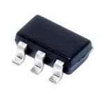
TPS72201, TPS72215 Actual Size TPS72216, TPS72218 www.ti.com (3,00 mm x 3,00 mm) SLVS390B – DECEMBER 2001 – REVISED MAY 2002 LOW INPUT VOLTAGE, CAP FREE 50-mA LOW-DROPOUT LINEAR REGULATORS FEATURES many other regulators that require 2.5-V or higher input voltages for operation, these regulators can be (cid:1) 50-mA LDO operated directly from two AAA batteries. Also, the (cid:1) Available in 1.5-V, 1.6-V, and 1.8-V typical quiescent current (ground pin current) is low, Fixed-Output and Adjustable Versions starting at 85 µA during normal operation and 1 µA in (cid:1) Low Input Voltage Requirement shutdown mode. Thus, these regulators can be (Down to 1.8 V) operated very efficiently and, in a battery-powered (cid:1) Small Output Capacitor, 0.1-µF application, help extend the longevity of the device. (cid:1) Dropout Voltage Typically 50 mV at 50 mA Similar LDO regulators require 1-µF or larger output (cid:1) Less Than 1 µA Quiescent Current in capacitors for stability. However, this regulator uses an internal compensation scheme that stabilizes the Shutdown Mode feedback loop over the full range of input voltages and (cid:1) Thermal Protection load currents with output capacitances as low as (cid:1) Over Current Limitation 0.1-µF. Ceramic capacitors of this size are relatively (cid:1) inexpensive and available in small footprints. 5-Pin SOT-23 (DBV) Package This family of regulators is particularly suited as a APPLICATIONS portable power supply solution due to its minimal board (cid:1) space requirement and 1.8-V minimum input voltage. Portable Communication Devices Being able to use two off-the-shelf, AAA, batteries (cid:1) Battery Powered Equipment makes system design easier and also reduces (cid:1) PCMCIA Cards component cost. Moreover, the solution will be more (cid:1) efficient than if a regulator with a higher input voltage is Personal Digital Assistants (cid:1) used. Modems (cid:1) Bar Code Scanners (cid:1) DBV PACKAGE Backup Power Supplies (TOP VIEW) (cid:1) SMPS Post Regulation (cid:1) IN 1 5 OUT Internet Audio GND 2 DESCRIPTION EN 3 4 NC/FB The TPS722xx family of LDO regulators is available in fixed voltage options that are commonly used to power the latest DSP’s and microcontrollers with an adjustable TPS72215 option ranging from 1.22 V to 2.5 V. These regulators 1.8 V 1.5 V IN OUT can be used in a wide variety of applications ranging EN GND from portable, battery-powered equipment to PC peripherals. The family features operation over a wide 0.1 µF 0.1 µF range of input voltages (1.8 V to 5.5 V) and low dropout voltage (50 mV at full load). Therefore, compared to Please be aware that an important notice concerning availability, standard warranty, and use in critical applications of TexasInstruments semiconductor products and disclaimers thereto appears at the end of this data sheet. PRODUCTION DATA information is current as of publication date. Products Copyright 2002, Texas Instruments Incorporated conform to specifications per the terms of Texas Instruments standard warranty. Production processing does not necessarily include testing of all parameters.
TPS72201, TPS72215 TPS72216, TPS72218 www.ti.com SLVS390B – DECEMBER 2001 – REVISED MAY 2002 These devices have limited built-in ESD protection. The leads should be shorted together or the device placed in conductive foam during storage or handling to prevent electrostatic damage to the MOS gates. ORDERING INFORMATION TJ VOLTAGE PACKAGE PART NUMBER SYMBOL Adjustable TPS72201DBVT(1) TPS72201DBVR(2) PELI 1.5 V SSOOTT-2233 TPS72215DBVT(1) TPS72215DBVR(2) PENI –4400°°CC ttoo 112255°°CC 1.6 V (DBV) TPS72216DBVT(1) TPS72216DBVR(2) PHGI 1.8 V TPS72218DBVT(1) TPS72218DBVR(2) PEMI (1)The DBVT indicates tape and reel of 250 parts. (2)The DBVR indicates tape and reel of 3000 parts. ABSOLUTE MAXIMUM RATINGS over operating free-air temperature range unless otherwise noted(1) TPS72201, TPS72215 TPS72216, TPS72218 Input voltage range (cid:2)(cid:3)(cid:4) –0.3 V to 7 V Voltage range at EN –0.3 V to 7 V Voltage on OUT, FB, NC –0.3 V to VI + 0.3 V Peak output current Internally limited ESD rating, HBM 3 kV Continuous total power dissipation See Dissipation Rating Table Operating virtual junction temperature range, TJ –40°C to 150°C Storage temperature range, Tstg –65°C to 150°C (1)Stresses beyond those listed under “absolute maximum ratings” may cause permanent damage to the device. These are stress ratings only, and functional operation of the device at these or any other conditions beyond those indicated under “recommended operating conditions” is not implied. Exposure to absolute-maximum-rated conditions for extended periods may affect device reliability. (2)All voltage values are with respect to network ground terminal. PACKAGE DISSIPATION RATING DERATING FACTOR TA ≤ 25°C TA = 70°C TA = 85°C BOARD PACKAGE RθJC RθJA ABOVE TA = 25°C POWER RATING POWER RATING POWER RATING Low K(1) DBV 65.8 °C/W 259 °C/W 3.9 mW/°C 386 mW 212 mW 154 mW High K(2) DBV 65.8 °C/W 180 °C/W 5.6 mW/°C 555 mW 305 mW 222 mW (1)The JEDEC Low K (1s) board design used to derive this data was a 3 inch x 3 inch, two-layer board with 2 ounce copper traces on top of the board. (2)The JEDEC High K (2s2p) board design used to derive this data was a 3 inch x 3 inch, multilayer board with 1 ounce internal power and ground planes and 2 ounce copper traces on top and bottom of the board. 2
TPS72201, TPS72215 TPS72216, TPS72218 www.ti.com SLVS390B – DECEMBER 2001 – REVISED MAY 2002 ELECTRICAL CHARACTERISTICS over recommended operating free-air temperature range, VI = VO(typ) + 1 V, IO= 1 mA, EN = VI, Co = 4.7 µF (unless otherwise noted) PARAMETER TEST CONDITIONS MIN TYP MAX UNIT VI Input voltage(1) 1.8 5.5 V IO Continuous output current 0 50 mA TJ Operating junction temperature –40 125 °C TPS72201 0 µA< IO < 50 mA,(1) 1.2 V ≤ VO ≤ 2.5 V 0.97 VO 1.03 VO TJ = 25°C 1.5 TTPPSS7722221155 0 µA< IO < 50 mA 2.5 V ≤ VI ≤ 5.5 V 1.455 1.545 VVOO OOuuttpuutt vvoollttaaggee TJ = 25°C 1.6 VV TTPPSS7722221166 0 µA< IO < 50 mA 2.6 V ≤ VI ≤ 5.5 V 1.552 1.648 TJ = 25°C 1.8 TTPPSS7722221188 0 µA< IO < 50 mA 2.5 V ≤ VI ≤ 5.5 V 1.746 1.854 TJ = 25°C 85 QQuuiieesscceenntt ccuurrrreenntt ((GGNNDD tteerrmmiinnaall 120 II(Q) current) IO = 50 mA TJ = 25°C 275 µAA IO = 50 mA 550 EN < 0.5 V, TJ = 25°C 0.01 SSttaannddbbyy ccuurrrreenntt µAA EN < 0.5 V 1 BW = 200 Hz to 100 kHz, Vn Output noise voltage TPS72215 TJ = 25°C Co = 1 µF 90 µV Vref Reference voltage TJ = 25°C 1.225 V f = 100 Hz, Co = 10 µF, TJ = 25°C, PSRR Ripple rejection IO = 50 mA See Note 1 48 dB Current limit See Note 2 175 525 mA OOuuttpuutt vvoollttaaggee lliinnee rreegguullaattiioonn TJ = 25°C 0.03 0.09 (∆VO/VO)(3) VVO + 11 VV < VVI ≤≤ 55.55 VV 0.1 %%//VV Output voltage load regulation TPS72218 0 < IO < 50 mA, TJ = 25°C 0.2 mV VIH EN high level input 1.4 V VIL EN low level input –0.2 0.4 V EN = 0 V –0.01 III EENN iinnppuutt ccuurrrreenntt µAA EN = IN –0.01 TPS72218 IO = 50 mA TJ = 25°C 50 VVDO DDrrooppoouutt vvoollttaaggee ((44)) TPS72201 IO = 50 mA 1.2 V ≤ VO ≤ 5.2 V 100 mmVV In Feedback input current TPS72201 1 µA Thermal shutdown temperature 170 °C Thermal shutdown hysteresis 20 °C (1)Minimum IN operating voltage is 1.8 V or VO(max) + VDO (max load), whichever is greater. (2)Test condition includes, output voltage VO = 1 V and pulse duration = 10 mS. (3)VImax = 5.5 V, VImin = (VO + 1) or 1.8 V whichever is greater. (cid:2) (cid:4) V 5.5V(cid:6)V Lineregulation(mV) (cid:1) (cid:2)%(cid:3)V(cid:4) (cid:5) O Imin (cid:5)1000 100 (4)Dropout voltage is defined as the differential voltage between VO and VI when VO drops 100 mV below the value measured with VI = VO + 1V. 3
TPS72201, TPS72215 TPS72216, TPS72218 www.ti.com SLVS390B – DECEMBER 2001 – REVISED MAY 2002 FUNCTIONAL BLOCK DIAGRAM—ADJUSTABLE VERSION TPS72201 IN OUT EN Current Limit / Thermal Vref Protection FB GND FUNCTIONAL BLOCK DIAGRAM—FIXED VERSION TPS72215/16/18 IN OUT EN Current Limit / Thermal Vref Protection GND NC (see Note 1) (1) This pin must be left floating and not connected to GND Terminal Functions TERMINAL II//OO DDEESSCCRRIIPPTTIIOONN NAME NO. GND 2 Ground EN 3 I Enable input IN 1 I Input supply voltage NC/FB 4 I NC = Not connected (see Note 6); FB = Feedback (adjustable option TPS72201) OUT 5 O Regulated output voltage 4
TPS72201, TPS72215 TPS72216, TPS72218 www.ti.com SLVS390B – DECEMBER 2001 – REVISED MAY 2002 TYPICAL CHARACTERISTICS TPS72218 TPS72218 TPS72218 OUTPUT VOLTAGE OUTPUT VOLTAGE GROUND CURRENT vs vs vs OUTPUT CURRENT JUNCTION TEMPERATURE JUNCTION TEMPERATURE 1.8002 1.8020 300 ut Voltage – V 111...788900900901 VCTJIo = == 2 21.58 µ° VFC put Voltage – V111...778990680000 VCIo = = 2 1.8 µ VF IO = 50 mA IO = 1 mA µCurrent – A 122505000 IO = 50 mA – Outp 1.7998 – OutO1.7940 Ground 100 IO = 10 mA O V V 1.7997 1.7920 50 VI = 2.8 V Co = 1 µF 1.7996 1.7900 0 0 10 20 30 40 50 –40–25–105 20 35 50 65 80 95 110125 –40–25–10 5 20 35 50 65 80 95 110125 IO – Output Current – mA TJ – Junction Temperature – °C TJ – Junction Temperature – °C Figure 1 Figure 2 Figure 3 TPS72218 TPS72218 TPS72218 GROUND CURRENT OUTPUT SPECTRAL NOISE DENSITY OUTPUT IMPEDANCE vs vs vs OUTPUT CURRENT FREQUENCY FREQUENCY 300 Hz 2.5 1 k 250 VCIo = = 2 1.8 µ VF TJ = 125°C µV/ VCIo = = 2 1.8 µ VF 100 VCIo = = 2 1.8 µ VF A 2 µGround Current – 112050000 TJ = –40°TCJ = 25°C pectral Noise Density – 1.51 IO = 50 mA ΩOutput Impedance – 01.101 IO = 1 mA IO = 50 mA S 0.5 50 ut 0.01 p ut O 0 0 0.001 0 5 10 15 20 25 30 35 40 45 50 100 1 k 10 k 100 k 1 10 100 1 k 10 k 100 k 1 M 10 M IO – Output Current – mA f – Frequency – Hz f – Frequency – Hz Figure 4 Figure 5 Figure 6 TPS72218 TPS72118 TPS72218 DROPOUT VOLTAGE POWER SUPPLY RIPPLE REJECTION OUTPUT VOLTAGE, ENABLE VOLTAGE vs vs vs JUNCTION TEMPERATURE FREQUENCY TIME (START-UP) 80 70 V ut Voltage – mV 45670000 VCIo = = 2 1.8 µ VF IO = 50 mA pple Rejection – dB 456000 VCIOIo = == 2 51.08 µ mVFA Enable Voltage – 2130 VEN V– DropoDO 123000 IO = 10 mA Power Supply Ri 123000 Output Voltage – V 102 VO VVICOIOo = = == 2 5 11.08 .µ 8 mVF VA 0 0 – O –40–25–105 20 35 50 65 80 95 110125 1 10 100 1 k 10 k 100 k 1 M V 0 50 100150200200300350400450500 TJ – Junction Temperature – °C f – Frequency – Hz t – Time – µs Figure 7 Figure 8 Figure 9 5
TPS72201, TPS72215 TPS72216, TPS72218 www.ti.com SLVS390B – DECEMBER 2001 – REVISED MAY 2002 TYPICAL CHARACTERISTICS TPS72218 TPS72218 LINE TRANSIENT RESPONSE mA LOAD TRANSIENT RESPONSE POWER UP / POWER DOWN oltage – V VI ICOo == 510 µ mFA Current – VCIo = = 2 1.8 µ VF V 56 VI V– Input VOutput Voltage –VI 23-..80118 VO ddVtI(cid:1)0µ.4sV ∆ – Change InVO– Output utput Voltage – mVIO–1100500000 ddIOt (cid:1)0µ.1sA Power Up / Power Down – 01234 VOCCRoiL = == 1 13 µ 6µF FΩ – O 0 0.1 0.2 0.3 0.4 0.5 0.6 0.7 0.8 0.9 1 O 0 50 100 150200250 300350 400450 500 0 10 20 30 40 50 60 70 80 90 100 V t – Time – ms t – Time – µs t – Time – ms Figure 10 Figure 11 Figure 12 TPS72201 DC DROPOUT VOLTAGE DROPOUT VOLTAGE MINIMUM REQUIRED INPUT VOLTAGE vs vs vs OUTPUT CURRENT INPUT VOLTAGE OUTPUT VOLTAGE 80 80 5.5 70 70 IO = 50 mA e – V 5 IO = 50 mA V g Dropout Voltage – m 34560000 TJ = 25°CTJ = 125°C opout Voltage – mV 34560000 TJ = 125°C TJ = 25°C Required Input Volta 34..5534 TJ = 25°CTJ = 125°C C Dr m 2.5 D 1200 TJ = –55°C V– DO 1200 TJ = –40°C – Minimu 1.52 TJ = –40°C 0 0 VI 1 0 5 10 15 20 25 30 35 40 45 50 1.8 2.5 3.3 4.0 4.8 5.5 1 1.5 2 2.5 3 3.5 4 4.5 5 5.5 IO – Output Current – mA VI – Input Voltage – V VO – Output Voltage – V Figure 13 Figure 14 Figure 15 6
TPS72201, TPS72215 TPS72216, TPS72218 www.ti.com SLVS390B – DECEMBER 2001 – REVISED MAY 2002 APPLICATION INFORMATION The TPS722xx family of low-dropout (LDO) regulators functions with a very low input voltage (>1.8 V). The dropout voltage is typically 50 mV at full load. Typical quiescent current (ground pin current) is only 85 µA and drops to 1 µA in the shutdown mode. DEVICE OPERATION The TPS722xx family can be operated at low input voltages due to low voltage circuit design techniques and a PMOS pass element that exhibits low dropout. A logic low on the enable input, EN, shuts off the output and reduces the supply current to less than 1 µA. EN may be tied to V in applications where the shutdown feature is not used. IN Current limiting and thermal protection prevent damage by excessive output current and/or power dissipation. The device switches into a constant-current mode at approximately 350 mA; further load reduces the output voltage instead of increasing the output current. The thermal protection shuts the regulator off if the junction temperature rises above 170°C. Recovery is automatic when the junction temperature drops approximately 20°C below the high temperature trip point. The PMOS pass element includes a back diode that safely conducts reverse current when the input voltage level drops below the output voltage level. A typical application circuit is shown in Figure 16. TPS722xx 1 VI IN OUT 5 VO 0.1 µF 4 3 NC EN + 0.1 µF GND 2 Figure 16. Typical Application Circuit DUAL SUPPLY APPLICATION In portable, battery-powered electronics, separate power rails for the DSP or microcontroller core voltage (V ) and I/O CORE peripherals (V ) are usually necessary. The TPS721xx family of LDO linear regulators is ideal for providing V for IO (CORE) the DSP or microcontroller. As shown in Figure 17, two AAA batteries provide an input voltage to a boost converter and the TPS72115 LDO linear regulator. The batteries combine input voltage ranges from 3.0 V down to 1.8 V near the end of their useful lives. Therefore, a boost converter is necessary to provide the typical 3.3 V needed for V , and the TPS72115 IO linear regulator provides a regulated V voltage, which in this example is 1.5 V. Although there is no explicit circuitry (CORE) to perform power-up sequencing of first V then V , the output of the linear regulator reaches its regulated voltage (CORE) IO much faster (<400 µs) than the output of any switching type boost converter due to the inherent slow start up of those types of converters. Assuming a boost converter with minimum V of 1.8 V is appropriately chosen, this power supply solution I can be used over the entire life of the two off-the-shelf AAA batteries. Thus, this solution is very efficient and the design time and overall cost of the solution is minimized. 7
TPS72201, TPS72215 TPS72216, TPS72218 www.ti.com SLVS390B – DECEMBER 2001 – REVISED MAY 2002 1.8 V – 3 V 3.3 V Boost Converter VIO DSP or Controller 1.8 V 1.5 V TPS72215 VCORE Two AAA Batteries Figure 17. Dual Supply Application Circuit EXTERNAL CAPACITOR REQUIREMENTS A 0.1-µF ceramic bypass capacitor is required on both the input and output for stability. Larger capacitors improve transient response, noise rejection, and ripple rejection. A higher value electrolytic input capacitor may be necessary if large, fast rise time load transient are anticipated, and/or there is significant input resistance from the device to the input power supply. POWER DISSIPATION AND JUNCTION TEMPERATURE Specified regulator operation is assured to a junction temperature of 125°C; the maximum junction temperature allowable without damaging the device is 150°C. This restriction limits the power dissipation the regulator can handle in any given application. To ensure the junction temperature is within acceptable limits, calculate the maximum allowable dissipation, P , and the actual dissipation, P , which must be less than or equal to P . D(max) D D(max) The maximum-power-dissipation limit is determined using the following equation: T max(cid:6)T P (cid:1) J A D(max) R(cid:1)JA Where: TJmax is the maximum allowable junction temperature. RθJA is the thermal resistance junction-to-ambient for the package, see the power dissipation rating table. TA is the ambient temperature. The regulator dissipation is calculated using: (cid:2) (cid:4) P (cid:1) V (cid:6)V (cid:5)I D I O O Power dissipation resulting from quiescent current is negligible. 8
TPS72201, TPS72215 TPS72216, TPS72218 www.ti.com SLVS390B – DECEMBER 2001 – REVISED MAY 2002 PROGRAMMING THE TPS72201 ADJUSTABLE LDO REGULATOR The output voltage of the TPS72201 adjustable regulator is programmed using an external resistor divider as shown in Figure 18. The output voltage is calculated using: (cid:2) (cid:4) V (cid:1)V (cid:5) 1(cid:7)R1 (1) O ref R2 Where: V = 1.225 V typ (the internal reference voltage) ref Resistors R1 and R2 should be chosen for approximately 10-µA divider current. Lower value resistors can be used but offer no inherent advantage and waste more power. Higher values should be avoided, as leakage currents at FB increase the output voltage error. The recommended design procedure is to choose R2 = 121kΩ to set the divider current at 10 µA and then calculate R1 using: (cid:2) (cid:4) V R1(cid:1) O (cid:6)1 (cid:5)R2 (2) V ref Where: Vref = 1.225 TPS72201 OUTPUT VOLTAGE PROGRAMMING GUIDE 1 VI IN OUTPUT DIVIDER RESISTANCE VOLTAGE (kΩ)† 0.1 µF (V) R1 R2 OUT 5 VO ≥1.7 V 2.5 127 121 3 R1 EN 3.3 205 121 4 ≤0.9 V FB †1% values shown. GND 0.1 µF R2 2 Figure 18. TPS72201 Adjustable LDO Regulator Programming REGULATOR PROTECTION The TPS722xx pass element has a built-in back diode that safely conducts reverse current when the input voltage drops below the output voltage (e.g., during power down). Current is conducted from the output to the input and is not internally limited. If extended reverse voltage is anticipated, external limiting might be appropriate. The TPS722xx also features internal current limiting and thermal protection. During normal operation, the TPS722xx limits output current to approximately 350 mA. When current limiting engages, the output voltage scales back linearly until the overcurrent condition ends. While current limiting is designed to prevent gross device failure, care should be taken not to exceed the power dissipation ratings of the package. If the temperature of the device exceeds 170°C, thermal-protection circuitry shuts it down. Once the device has cooled down to below 150°C, regulator operation resumes. 9
PACKAGE OPTION ADDENDUM www.ti.com 30-Mar-2019 PACKAGING INFORMATION Orderable Device Status Package Type Package Pins Package Eco Plan Lead/Ball Finish MSL Peak Temp Op Temp (°C) Device Marking Samples (1) Drawing Qty (2) (6) (3) (4/5) TPS72201DBVR ACTIVE SOT-23 DBV 5 3000 Green (RoHS CU NIPDAU Level-1-260C-UNLIM -40 to 125 PELI & no Sb/Br) TPS72201DBVRG4 ACTIVE SOT-23 DBV 5 3000 Green (RoHS CU NIPDAU Level-1-260C-UNLIM -40 to 125 PELI & no Sb/Br) TPS72201DBVT ACTIVE SOT-23 DBV 5 250 Green (RoHS CU NIPDAU Level-1-260C-UNLIM -40 to 125 PELI & no Sb/Br) TPS72215DBVT ACTIVE SOT-23 DBV 5 250 Green (RoHS CU NIPDAU Level-1-260C-UNLIM -40 to 125 PENI & no Sb/Br) TPS72215DBVTG4 ACTIVE SOT-23 DBV 5 250 Green (RoHS CU NIPDAU Level-1-260C-UNLIM -40 to 125 PENI & no Sb/Br) TPS72216DBVT ACTIVE SOT-23 DBV 5 250 Green (RoHS CU NIPDAU Level-1-260C-UNLIM -40 to 125 PHGI & no Sb/Br) TPS72218DBVR ACTIVE SOT-23 DBV 5 3000 Green (RoHS CU NIPDAU Level-1-260C-UNLIM -40 to 125 PEMI & no Sb/Br) TPS72218DBVT ACTIVE SOT-23 DBV 5 250 Green (RoHS CU NIPDAU Level-1-260C-UNLIM -40 to 125 PEMI & no Sb/Br) TPS72218DBVTG4 ACTIVE SOT-23 DBV 5 250 Green (RoHS CU NIPDAU Level-1-260C-UNLIM -40 to 125 PEMI & no Sb/Br) (1) The marketing status values are defined as follows: ACTIVE: Product device recommended for new designs. LIFEBUY: TI has announced that the device will be discontinued, and a lifetime-buy period is in effect. NRND: Not recommended for new designs. Device is in production to support existing customers, but TI does not recommend using this part in a new design. PREVIEW: Device has been announced but is not in production. Samples may or may not be available. OBSOLETE: TI has discontinued the production of the device. (2) RoHS: TI defines "RoHS" to mean semiconductor products that are compliant with the current EU RoHS requirements for all 10 RoHS substances, including the requirement that RoHS substance do not exceed 0.1% by weight in homogeneous materials. Where designed to be soldered at high temperatures, "RoHS" products are suitable for use in specified lead-free processes. TI may reference these types of products as "Pb-Free". RoHS Exempt: TI defines "RoHS Exempt" to mean products that contain lead but are compliant with EU RoHS pursuant to a specific EU RoHS exemption. Green: TI defines "Green" to mean the content of Chlorine (Cl) and Bromine (Br) based flame retardants meet JS709B low halogen requirements of <=1000ppm threshold. Antimony trioxide based flame retardants must also meet the <=1000ppm threshold requirement. (3) MSL, Peak Temp. - The Moisture Sensitivity Level rating according to the JEDEC industry standard classifications, and peak solder temperature. Addendum-Page 1
PACKAGE OPTION ADDENDUM www.ti.com 30-Mar-2019 (4) There may be additional marking, which relates to the logo, the lot trace code information, or the environmental category on the device. (5) Multiple Device Markings will be inside parentheses. Only one Device Marking contained in parentheses and separated by a "~" will appear on a device. If a line is indented then it is a continuation of the previous line and the two combined represent the entire Device Marking for that device. (6) Lead/Ball Finish - Orderable Devices may have multiple material finish options. Finish options are separated by a vertical ruled line. Lead/Ball Finish values may wrap to two lines if the finish value exceeds the maximum column width. Important Information and Disclaimer:The information provided on this page represents TI's knowledge and belief as of the date that it is provided. TI bases its knowledge and belief on information provided by third parties, and makes no representation or warranty as to the accuracy of such information. Efforts are underway to better integrate information from third parties. TI has taken and continues to take reasonable steps to provide representative and accurate information but may not have conducted destructive testing or chemical analysis on incoming materials and chemicals. TI and TI suppliers consider certain information to be proprietary, and thus CAS numbers and other limited information may not be available for release. In no event shall TI's liability arising out of such information exceed the total purchase price of the TI part(s) at issue in this document sold by TI to Customer on an annual basis. Addendum-Page 2
PACKAGE MATERIALS INFORMATION www.ti.com 31-Mar-2019 TAPE AND REEL INFORMATION *Alldimensionsarenominal Device Package Package Pins SPQ Reel Reel A0 B0 K0 P1 W Pin1 Type Drawing Diameter Width (mm) (mm) (mm) (mm) (mm) Quadrant (mm) W1(mm) TPS72201DBVR SOT-23 DBV 5 3000 180.0 8.4 3.2 3.2 1.4 4.0 8.0 Q3 TPS72201DBVR SOT-23 DBV 5 3000 178.0 9.0 3.23 3.17 1.37 4.0 8.0 Q3 TPS72201DBVT SOT-23 DBV 5 250 178.0 9.0 3.23 3.17 1.37 4.0 8.0 Q3 TPS72201DBVT SOT-23 DBV 5 250 180.0 8.4 3.2 3.2 1.4 4.0 8.0 Q3 TPS72215DBVT SOT-23 DBV 5 250 178.0 9.0 3.23 3.17 1.37 4.0 8.0 Q3 TPS72216DBVT SOT-23 DBV 5 250 180.0 8.4 3.2 3.2 1.4 4.0 8.0 Q3 TPS72218DBVR SOT-23 DBV 5 3000 178.0 9.0 3.23 3.17 1.37 4.0 8.0 Q3 TPS72218DBVT SOT-23 DBV 5 250 178.0 9.0 3.3 3.2 1.4 4.0 8.0 Q3 PackMaterials-Page1
PACKAGE MATERIALS INFORMATION www.ti.com 31-Mar-2019 *Alldimensionsarenominal Device PackageType PackageDrawing Pins SPQ Length(mm) Width(mm) Height(mm) TPS72201DBVR SOT-23 DBV 5 3000 203.0 203.0 35.0 TPS72201DBVR SOT-23 DBV 5 3000 180.0 180.0 18.0 TPS72201DBVT SOT-23 DBV 5 250 180.0 180.0 18.0 TPS72201DBVT SOT-23 DBV 5 250 203.0 203.0 35.0 TPS72215DBVT SOT-23 DBV 5 250 180.0 180.0 18.0 TPS72216DBVT SOT-23 DBV 5 250 203.0 203.0 35.0 TPS72218DBVR SOT-23 DBV 5 3000 180.0 180.0 18.0 TPS72218DBVT SOT-23 DBV 5 250 180.0 180.0 18.0 PackMaterials-Page2
PACKAGE OUTLINE DBV0005A SOT-23 - 1.45 mm max height SCALE 4.000 SMALL OUTLINE TRANSISTOR C 3.0 2.6 0.1 C 1.75 1.45 B A 1.45 MAX PIN 1 INDEX AREA 1 5 2X 0.95 3.05 2.75 1.9 1.9 2 4 3 0.5 5X 0.3 0.15 0.2 C A B (1.1) TYP 0.00 0.25 GAGE PLANE 0.22 TYP 0.08 8 TYP 0.6 0 0.3 TYP SEATING PLANE 4214839/D 11/2018 NOTES: 1. All linear dimensions are in millimeters. Any dimensions in parenthesis are for reference only. Dimensioning and tolerancing per ASME Y14.5M. 2. This drawing is subject to change without notice. 3. Refernce JEDEC MO-178. 4. Body dimensions do not include mold flash, protrusions, or gate burrs. Mold flash, protrusions, or gate burrs shall not exceed 0.15 mm per side. www.ti.com
EXAMPLE BOARD LAYOUT DBV0005A SOT-23 - 1.45 mm max height SMALL OUTLINE TRANSISTOR PKG 5X (1.1) 1 5 5X (0.6) SYMM (1.9) 2 2X (0.95) 3 4 (R0.05) TYP (2.6) LAND PATTERN EXAMPLE EXPOSED METAL SHOWN SCALE:15X SOLDER MASK SOLDER MASK METAL UNDER METAL OPENING OPENING SOLDER MASK EXPOSED METAL EXPOSED METAL 0.07 MAX 0.07 MIN ARROUND ARROUND NON SOLDER MASK SOLDER MASK DEFINED DEFINED (PREFERRED) SOLDER MASK DETAILS 4214839/D 11/2018 NOTES: (continued) 5. Publication IPC-7351 may have alternate designs. 6. Solder mask tolerances between and around signal pads can vary based on board fabrication site. www.ti.com
EXAMPLE STENCIL DESIGN DBV0005A SOT-23 - 1.45 mm max height SMALL OUTLINE TRANSISTOR PKG 5X (1.1) 1 5 5X (0.6) SYMM 2 (1.9) 2X(0.95) 3 4 (R0.05) TYP (2.6) SOLDER PASTE EXAMPLE BASED ON 0.125 mm THICK STENCIL SCALE:15X 4214839/D 11/2018 NOTES: (continued) 7. Laser cutting apertures with trapezoidal walls and rounded corners may offer better paste release. IPC-7525 may have alternate design recommendations. 8. Board assembly site may have different recommendations for stencil design. www.ti.com
IMPORTANTNOTICEANDDISCLAIMER TIPROVIDESTECHNICALANDRELIABILITYDATA(INCLUDINGDATASHEETS),DESIGNRESOURCES(INCLUDINGREFERENCE DESIGNS),APPLICATIONOROTHERDESIGNADVICE,WEBTOOLS,SAFETYINFORMATION,ANDOTHERRESOURCES“ASIS” ANDWITHALLFAULTS,ANDDISCLAIMSALLWARRANTIES,EXPRESSANDIMPLIED,INCLUDINGWITHOUTLIMITATIONANY IMPLIEDWARRANTIESOFMERCHANTABILITY,FITNESSFORAPARTICULARPURPOSEORNON-INFRINGEMENTOFTHIRD PARTYINTELLECTUALPROPERTYRIGHTS. TheseresourcesareintendedforskilleddevelopersdesigningwithTIproducts.Youaresolelyresponsiblefor(1)selectingtheappropriate TIproductsforyourapplication,(2)designing,validatingandtestingyourapplication,and(3)ensuringyourapplicationmeetsapplicable standards,andanyothersafety,security,orotherrequirements.Theseresourcesaresubjecttochangewithoutnotice.TIgrantsyou permissiontousetheseresourcesonlyfordevelopmentofanapplicationthatusestheTIproductsdescribedintheresource.Other reproductionanddisplayoftheseresourcesisprohibited.NolicenseisgrantedtoanyotherTIintellectualpropertyrightortoanythird partyintellectualpropertyright.TIdisclaimsresponsibilityfor,andyouwillfullyindemnifyTIanditsrepresentativesagainst,anyclaims, damages,costs,losses,andliabilitiesarisingoutofyouruseoftheseresources. TI’sproductsareprovidedsubjecttoTI’sTermsofSale(www.ti.com/legal/termsofsale.html)orotherapplicabletermsavailableeitheron ti.comorprovidedinconjunctionwithsuchTIproducts.TI’sprovisionoftheseresourcesdoesnotexpandorotherwisealterTI’sapplicable warrantiesorwarrantydisclaimersforTIproducts. MailingAddress:TexasInstruments,PostOfficeBox655303,Dallas,Texas75265 Copyright©2019,TexasInstrumentsIncorporated