ICGOO在线商城 > TPS657051YZHR
 Datasheet下载
- 型号: TPS657051YZHR
- 制造商: Texas Instruments
- 库位|库存: xxxx|xxxx
- 要求:
| 数量阶梯 | 香港交货 | 国内含税 |
| +xxxx | $xxxx | ¥xxxx |
查看当月历史价格
查看今年历史价格
TPS657051YZHR产品简介:
ICGOO电子元器件商城为您提供TPS657051YZHR由Texas Instruments设计生产,在icgoo商城现货销售,并且可以通过原厂、代理商等渠道进行代购。 提供TPS657051YZHR价格参考以及Texas InstrumentsTPS657051YZHR封装/规格参数等产品信息。 你可以下载TPS657051YZHR参考资料、Datasheet数据手册功能说明书, 资料中有TPS657051YZHR详细功能的应用电路图电压和使用方法及教程。
| 参数 | 数值 |
| 产品目录 | 集成电路 (IC) |
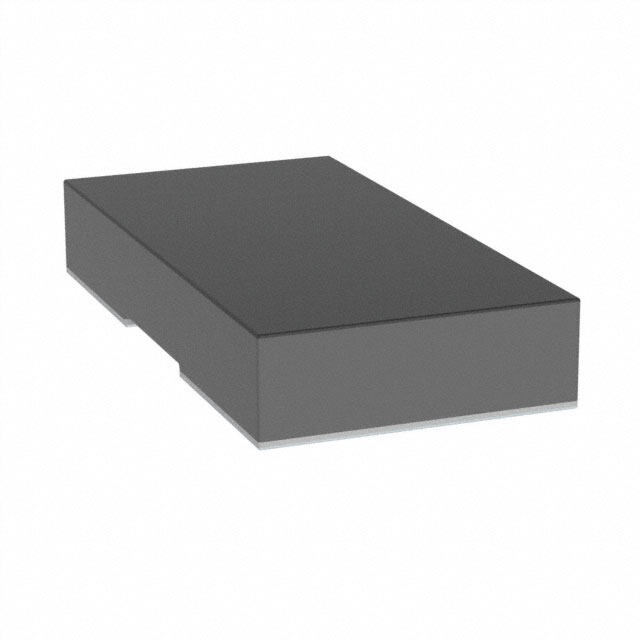
| 描述 | IC PMU 3CH CONV/LDO 16DSBGA |
| 产品分类 | |
| 品牌 | Texas Instruments |
| 数据手册 | |
| 产品图片 | |
| 产品型号 | TPS657051YZHR |
| rohs | 无铅 / 符合限制有害物质指令(RoHS)规范要求 |
| 产品系列 | - |
| 产品目录页面 | |
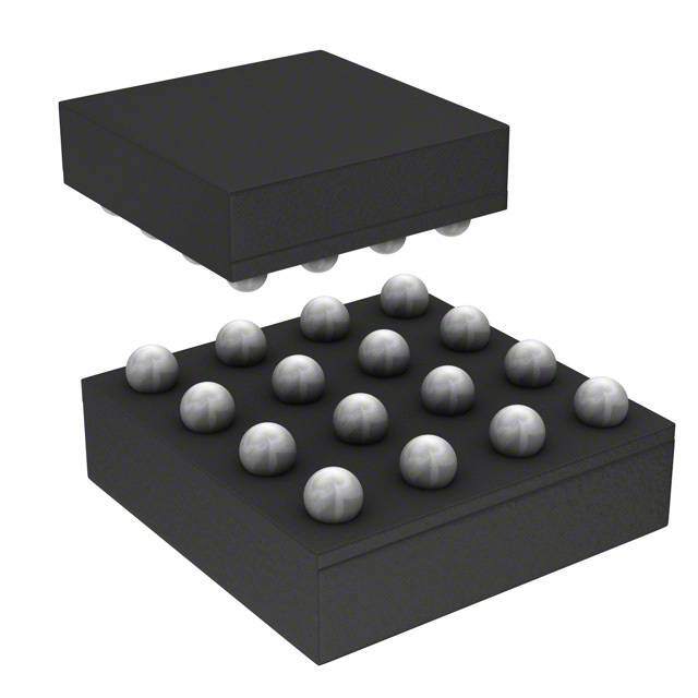
| 供应商器件封装 | 16-DSBGA(2x2) |
| 其它名称 | 296-25867-6 |
| 包装 | Digi-Reel® |
| 安装类型 | 表面贴装 |
| 封装/外壳 | 16-UFBGA,DSBGA |
| 工作温度 | -40°C ~ 85°C |
| 应用 | 照相机 |
| 标准包装 | 1 |
| 电压-电源 | 3.3 V ~ 6 V |
| 电流-电源 | - |


- 商务部:美国ITC正式对集成电路等产品启动337调查
- 曝三星4nm工艺存在良率问题 高通将骁龙8 Gen1或转产台积电
- 太阳诱电将投资9.5亿元在常州建新厂生产MLCC 预计2023年完工
- 英特尔发布欧洲新工厂建设计划 深化IDM 2.0 战略
- 台积电先进制程称霸业界 有大客户加持明年业绩稳了
- 达到5530亿美元!SIA预计今年全球半导体销售额将创下新高
- 英特尔拟将自动驾驶子公司Mobileye上市 估值或超500亿美元
- 三星加码芯片和SET,合并消费电子和移动部门,撤换高东真等 CEO
- 三星电子宣布重大人事变动 还合并消费电子和移动部门
- 海关总署:前11个月进口集成电路产品价值2.52万亿元 增长14.8%


PDF Datasheet 数据手册内容提取
Product Sample & Technical Tools & Support & Folder Buy Documents Software Community TPS657051,TPS657052 SLVSA08A–FEBRUARY2010–REVISEDSEPTEMBER2015 TPS65705x PMU for Embedded Camera Module 1 Features 3 Description • Two400-mAStep-DownConverters The TPS65705x devices are small power 1 management units targeted for embedded camera • Upto92%Efficiency module or other portable low-power consumer-end • VIN RangeforDC-DCConverter equipments. The device contains two highly efficient From3.3Vto6V step-down converters, a low dropout linear regulator, • 2.25-MHzFixed-FrequencyOperation and additional supporting functions. The 2.25-MHz step-downconverterentersalow-powermodeatlight • PowerSaveModeatLightLoadCurrent load for maximum efficiency across the widest • OutputVoltageAccuracyinPWMMode±1.5% possible range of load currents. For low-noise • 100%DutyCycleforLowestDropout applications, the device can be forced into fixed- frequency PWM mode using the MODE pin. The • 180° Out-of-PhaseOperation device allows the use of small inductors and • 1GeneralPurpose200-mALDO capacitors to achieve a small sized solution. The • V RangeforLDOFrom1.7Vto6.0V TPS65705xprovidesanoutputcurrentofupto IN • Availableina16-BallDSBGA(WCSP)With0.5- 400 mA on both DC-DC converters and integrates mmPitch one 200-mA LDO with different output settings. The LDO operates with an input voltage range from 1.7 V to 6 V, thus allowing it to be supplied from the output 2 Applications of the step-down converter or directly from the • DigitalCameras systemvoltage. • PortableMediaPlayers The TPS65705x comes in a small 16-pin wafer chip • HandheldEquipment scalepackage(WCSP)with0.5-mmballpitch. DeviceInformation(1) PARTNUMBER PACKAGE BODYSIZE(NOM) TPS657051 DSBGA(16) 2.08mm×2.08mm TPS657052 (1) For all available packages, see the orderable addendum at theendofthedatasheet. ApplicationCircuit VCC TPS657051/52 VIN1 2.2μH L1 Vout1 MODE DCDC1 EN1 400mA 10mF FB1 10uF PGND CLK0° 2.25MHz Oscillator CLK180° 2.2μH L2 VIN2 Vout2 DCDC2 EN2 400mA FB2 10mF PGND VINLDO VLDO Vout3 ENLDO LDO 2.2mF 200mA AGND 1 An IMPORTANT NOTICE at the end of this data sheet addresses availability, warranty, changes, use in safety-critical applications, intellectualpropertymattersandotherimportantdisclaimers.PRODUCTIONDATA.
TPS657051,TPS657052 SLVSA08A–FEBRUARY2010–REVISEDSEPTEMBER2015 www.ti.com Table of Contents 1 Features.................................................................. 1 8.3 FeatureDescription.................................................12 2 Applications........................................................... 1 8.4 DeviceFunctionalModes........................................15 3 Description............................................................. 1 9 ApplicationandImplementation........................ 16 4 RevisionHistory..................................................... 2 9.1 ApplicationInformation............................................16 9.2 TypicalApplication .................................................16 5 DeviceOptions....................................................... 3 10 PowerSupplyRecommendations..................... 18 6 PinConfigurationandFunctions......................... 3 11 Layout................................................................... 19 7 Specifications......................................................... 4 11.1 LayoutGuidelines.................................................19 7.1 AbsoluteMaximumRatings......................................4 11.2 LayoutExample....................................................19 7.2 ESDRatings..............................................................4 12 DeviceandDocumentationSupport................. 20 7.3 RecommendedOperatingConditions.......................5 7.4 ThermalInformation..................................................5 12.1 DeviceSupport......................................................20 7.5 ElectricalCharacteristics...........................................5 12.2 RelatedLinks........................................................20 7.6 DissipationRatings...................................................7 12.3 CommunityResources..........................................20 7.7 TypicalCharacteristics..............................................7 12.4 Trademarks...........................................................20 12.5 ElectrostaticDischargeCaution............................20 8 DetailedDescription............................................ 12 12.6 Glossary................................................................20 8.1 Overview.................................................................12 13 Mechanical,Packaging,andOrderable 8.2 FunctionalBlockDiagram.......................................12 Information........................................................... 20 4 Revision History NOTE:Pagenumbersforpreviousrevisionsmaydifferfrompagenumbersinthecurrentversion. ChangesfromOriginal(February2010)toRevisionA Page • AddedESDRatingstable,FeatureDescriptionsection,DeviceFunctionalModes,ApplicationandImplementation section,PowerSupplyRecommendationssection,Layoutsection,DeviceandDocumentationSupportsection,and Mechanical,Packaging,andOrderableInformationsection.................................................................................................. 1 • ChangedfootnoteerrorforDeviceOptionstable................................................................................................................... 3 2 SubmitDocumentationFeedback Copyright©2010–2015,TexasInstrumentsIncorporated ProductFolderLinks:TPS657051 TPS657052
TPS657051,TPS657052 www.ti.com SLVSA08A–FEBRUARY2010–REVISEDSEPTEMBER2015 5 Device Options PARTNO.(1) SIZEFORDSBGAVERSION OPTIONS I2C DC-DC13.3VFIX,DC-DC21.8VFIX D=2076µm±25µm TPS657051 DC-DCCONVERTERS400mA, N/A E=2076µm±25µm LDOVOUT3VFIX,200mA DC-DC13.3VFIX,DC-DC21.8VFIX D=2076µm±25µm TPS657052 DC-DCCONVERTERS400mA, N/A E=2076µm±25µm LDOVOUT2.8VFIX,200mA (1) Forthemostcurrentpackageandorderinginformation,seetheMechanical,Packaging,andOrderableInformationsectionattheendof thisdocument,orseetheTIwebsiteatwww.ti.com. 6 Pin Configuration and Functions TPS657051YZHPackage 16-PinDSBGA TopView 2075um VIN VVVLLLDDDOOO AAAGGGNNNDDD LVDINO VVVCCCCCC LDO AA11 VVIINN11 EENN11 EENN22 VVIINN22 BB11 EENN 2075um LL11 MMOODDEE LL22 LLDDOO CC11 PPGGNNDD PGND FFBB11 FFBB22 PG2ND 11 2 DD11 DD22 DD33 DD44 TPS657052YZHPackage 16-PinDSBGA TopView 2075um VIN VVVCCCCCC LLVVDDIINNOO AAAAGGGGNNNNDDDD VVVVLLLLDDDDOOOO LDO AA11 VVVIIINNN222 EEENNN222 EEENNN111 VVVIIINNN111 BB11 m LLL222 MMMMOOOODDDDEEEE LLLEEEEDDDNNNNOOO LLL111 2075u LDO CC11 PPPGGG22NNNDDD FFFBBB222 FFFBBB111 PPPGGGNNNDDD 2 DD44 DD33 DD22 111 DD11 Copyright©2010–2015,TexasInstrumentsIncorporated SubmitDocumentationFeedback 3 ProductFolderLinks:TPS657051 TPS657052
TPS657051,TPS657052 SLVSA08A–FEBRUARY2010–REVISEDSEPTEMBER2015 www.ti.com PinFunctions PIN I/O DESCRIPTION NO. NAME A1 VLDO O OutputvoltagefromLDO A2 AGND — Analogground A3 VINLDO I InputvoltagepinforLDO A4(1) VCC I SupplyInputforinternalreference,hastobeconnectedtoVIN1/VIN2 B1(2) VIN1 I Inputvoltagepinforbuckconverter1 B2 EN1 I Activelyhighenableinputvoltageforbuckconverter1 B3 EN2 I Activelyhighenableinputvoltageforbuckconverter2 B4(2) VIN2 I Inputvoltagepinforbuckconverter2 C1 L1 O Switchoutputfrombuckconverter1 C2 ENLDO I ActivelyhighenableinputvoltageforLDO SetlowtoenablePowerSaveMode.PullingthisPINtohighforcesthedevicetooperatein C3 MODE I PWMmodeoverthewholeloadrange. C4 L2 O Switchoutputfrombuckconverter2 D1 PGND1 — Powerground D2 FB1 I Feedbackinputfrombuckconverter1 D3 FB2 I Feedbackinputfrombuckconverter2 D4 PGND2 — Powerground (1) VCCmustbethehighestinputforthedevicetofunctioncorrectly. (2) VIN1/VIN2mustbeconnectedtoVCC. 7 Specifications 7.1 Absolute Maximum Ratings overoperatingfree-airtemperaturerange(unlessotherwisenoted) MIN MAX UNIT InputvoltageonallpinsexceptA/PGNDpinswithrespecttoAGND –0.3 7 V VoltageonpinVLDO1withrespecttoAGND –0.3 3.6 V L1,VLDO1,VINLDO1,PGND 600 mA Current AGND 20 mA Allotherpins 3 mA Continuoustotalpowerdissipation SeeDissipationRatings Operatingfree-airtemperature,T –40 85 °C A Maximumjunctiontemperature,T 125 °C J Storagetemperature,T –65 150 °C stg 7.2 ESD Ratings VALUE UNIT Electrostatic Humanbodymodel(HBM),perANSI/ESDA/JEDECJS-001(1) ±2000 V V (ESD) discharge Chargeddevicemodel(CDM),perJEDECspecificationJESD22-C101(2) ±500 (1) JEDECdocumentJEP155statesthat500-VHBMallowssafemanufacturingwithastandardESDcontrolprocess. (2) JEDECdocumentJEP157statesthat250-VCDMallowssafemanufacturingwithastandardESDcontrolprocess. 4 SubmitDocumentationFeedback Copyright©2010–2015,TexasInstrumentsIncorporated ProductFolderLinks:TPS657051 TPS657052
TPS657051,TPS657052 www.ti.com SLVSA08A–FEBRUARY2010–REVISEDSEPTEMBER2015 7.3 Recommended Operating Conditions overoperatingfree-airtemperaturerange(unlessotherwisenoted) MIN NOM MAX UNIT V Inputvoltageforstep-downconverterDCDC1andDCDC2 3.3 6 V IN1/2 I OutputcurrentatL 400 mA OUTDCDC1/2 L InductoratL 1.5 2.2 4.7 µH V InputvoltageforLDO 1.7 6.0 V INLDO I OutputcurrentatLDO 200 mA LDO C InputCapacitoratV andV 4.7 µF INDCDC1/2 IN1 IN2 C OutputCapacitoratV ,V 4.7 10 22 µF OUTDCDC1/2 OUT1 OUT2 C InputCapacitoratV 2.2 µF INLDO INLDO C OutputCapacitoratV 2.2 µF OUTLDO LDO T Operatingambienttemperature –40 85 °C A T Operatingjunctiontemperature –40 125 °C J 7.4 Thermal Information TPS65705x THERMALMETRIC(1) YZH(DSBGA) UNIT 16PINS R Junction-to-ambientthermalresistance 75 °C/W θJA R Junction-to-case(top)thermalresistance 22 °C/W θJC(top) R Junction-to-boardthermalresistance 26 °C/W θJB ψ Junction-to-topcharacterizationparameter 0.2 °C/W JT ψ Junction-to-boardcharacterizationparameter 24 °C/W JB R Junction-to-case(bottom)thermalresistance N/A °C/W θJC(bot) (1) Formoreinformationabouttraditionalandnewthermalmetrics,seetheSemiconductorandICPackageThermalMetricsapplication report,SPRA953. 7.5 Electrical Characteristics Unlessotherwisenoted:V =V =V =3.6V,L=LQMP21P2.2µH,C =10µF,C =2.2µF,T =–40°C IN1 IN2 INLDO OUTDCDCx OUTLDO A to+85°C PARAMETER TESTCONDITIONS MIN TYP MAX UNIT SUPPLYCURRENT DCDC1andDCDC2enabled,I =0mA, OUT MODE=0 40 µA (PFMmode),LDOdisabled DCDC1orDCDC2enabled,I =0mA, OperatingquiescentcurrentDCDCx OUT MODE=0 25 µA IQ (PFMmode),LDOdisabled DCDC1orDCDC2enabled,I =0mA. OUT 4 mA MODE=1(forcedPWMmode),LDOdisabled DCDC1andDCDC2disabled,LDOenabled. OperatingquiescentcurrentLDO 25 37 µA IOUT=0mA I Shutdowncurrent DCDC1,DCDC2,andLDOdisable 5 12 µA SD DIGITALPINS(EN1,EN2,ENLDO,MODE) High-levelinputvoltageforEN1, V 1.2 VCC V IH EN2,ENLDO,MODE Low-levelinputvoltageforEN1, V 0.4 V IL EN2,ENLDO,MODE EN1,EN2,ENLDO,MODEtiedtoGND I Inputleakagecurrent 0.01 0.1 μA LKG orV =V IN IN2 STEP-DOWNCONVERTERS V InputvoltageforDCDC1 3.3 6 V IN1 Copyright©2010–2015,TexasInstrumentsIncorporated SubmitDocumentationFeedback 5 ProductFolderLinks:TPS657051 TPS657052
TPS657051,TPS657052 SLVSA08A–FEBRUARY2010–REVISEDSEPTEMBER2015 www.ti.com Electrical Characteristics (continued) Unlessotherwisenoted:V =V =V =3.6V,L=LQMP21P2.2µH,C =10µF,C =2.2µF,T =–40°C IN1 IN2 INLDO OUTDCDCx OUTLDO A to+85°C PARAMETER TESTCONDITIONS MIN TYP MAX UNIT V InputvoltageforDCDC2 3.3 6 V IN2 Internalundervoltagelockout V =V falling 2.15 2.2 2.25 V threshold IN1 IN2 UVLO Internalundervoltagelockout V =V rising 120 mV thresholdhysteresis IN1 IN2 POWERSWITCH High-sideMOSFETON-resistance V =V =3.6V 350 750 mΩ IN1 IN2 R DS(ON) Low-sideMOSFETON-resistance V =V =3.6V 350 600 mΩ IN1 IN2 I Forwardcurrentlimit 3.3V≤V =V ≤6V 550 650 770 mA LIMF IN1 IN2 I DCDC1/DCDC2outputcurrent V =V >3.3V,L=2.2µH 400 mA OUTDCDC1/2 IN1 IN2 OSCILLATOR f Oscillatorfrequency 2.03 2.25 2.48 MHz SW OUTPUT V DCDC1defaultoutputvoltage V =V ≥3.3V 3.3 V OUT1 IN1 IN2 V DCDC2defaultoutputvoltage V =V ≥3.3V 1.8 V OUT2 IN1 IN2 I FBpininputcurrent DC-DCconverterdisabled 0.1 µA FB V =V =3.3Vto6V,+1%voltage IN1 IN2 DCoutputvoltageaccuracy(1) positioningactive;PFMoperation,0mA<I +1% +3% OUT <I OUTMAX V OUT V =V =3.3Vto6V,PWMoperation, DCoutputvoltageaccuracy IN1 IN2 –1.5% +1.5% 0mA<I <I OUT OUTMAX DCoutputvoltageloadregulation PWMoperation 0.5 %/A t Start-uptime TimefromactiveENtoStartswitching 200 µs Start t V ramptime Timetorampfrom5%to95%ofV 250 µs Ramp OUT OUT InternaldischargeresistoratL1or R L2 DCDC1orDCDC2disabled 250 400 600 Ω DIS (TPS657051Only) THERMALPROTECTIONSEPARATELYFORDCDC1,DCDC2ANDLDO1 T Thermalshutdown Increasingjunctiontemperature 150 °C SD Thermalshudownhysteresis Decreasingjunctiontemperature 30 °C VLDO,LOWDROPOUTREGULATOR V InputvoltagerangeforLDO 1.7 6 V INLDO TPS657051LDOdefaultoutput VLDO voltage(2) 3 V TPS657052LDOdefaultoutput VLDO voltage(3) 2.8 V I OutputcurrentforLDO 200 mA O I LDOshortcircuitcurrentlimit V =GND 340 400 550 mA SC LDO DropoutvoltageatLDO I =200mA 200 mV O OutputvoltageaccuracyforLDO I =100mA,V =2.8V –2% +2% O OUT V =V +0.5V(min.1.7V)to6V, LineregulationforLDO INLDO LDO –1% 1% I =50mA O LoadregulationforLDO I =1mAto200mAforLDO –1% 1% O f ≤10kHz,C ≥2.2µfVin=5V, PSRR Powersupplyrejectionratio NOISE OUT 50 dB Vout=2.8V,IOUT=100mA Vn Ouputnoisevoltage Vout=2.8V,BW=10Hzto100kHz 160 µVRMS (1) InPowerSaveMode(PFM),theinternalreferencevoltageis1.01×Vref. (2) VINLDO>3V (3) VINLDO>2.8V 6 SubmitDocumentationFeedback Copyright©2010–2015,TexasInstrumentsIncorporated ProductFolderLinks:TPS657051 TPS657052
TPS657051,TPS657052 www.ti.com SLVSA08A–FEBRUARY2010–REVISEDSEPTEMBER2015 Electrical Characteristics (continued) Unlessotherwisenoted:V =V =V =3.6V,L=LQMP21P2.2µH,C =10µF,C =2.2µF,T =–40°C IN1 IN2 INLDO OUTDCDCx OUTLDO A to+85°C PARAMETER TESTCONDITIONS MIN TYP MAX UNIT Internalsoft-startwhenLDOisenabled;Timeto t V ramptime 200 µs Ramp OUT rampfrom5%to95%ofV OUT R InternaldischargeresistoratVLDO LDOdisabled 250 400 550 Ω DIS 7.6 Dissipation Ratings T ≤25°C DERATINGFACTOR T =70°C T =85°C DEVICE PACKAGE R A A A θJA POWERRATING ABOVET =25°C POWERRATING POWERRATING A TPS657051/52(1) YZH 185 540mW 5.4mW 297mW 216mW TPS657051/52(2) YZH 75 1.3W 13.3mW 0.7W 0.5W (1) TheJEDEClow-K(1s)boardusedtoderivethisdatawasa3in×3in,two-layerboardwith2-ouncecoppertracesontopoftheboard. (2) TheJEDEChigh-K(2s2p)boardusedtoderivethisdatawasa3in×3in,multilayerboardwith1-ounceinternalpowerandground. 7.7 Typical Characteristics Table1.TableOfGraphs FIGURE EfficiencyDC-DC(VDCDC=3.3V),L=BRC16081.5µH vsLoadcurrent/PFMmode Figure1 EfficiencyDC-DC(VDCDC=3.3V),L=BRC16081.5µH vsLoadcurrent/PWMmode Figure2 EfficiencyDC-DC(VDCDC=1.8V),L=BRC16081.5µH vsLoadcurrent/PFMmode Figure3 EfficiencyDC-DC(VDCDC=1.8V),L=BRC16081.5µH vsLoadcurrent/PWMmode Figure4 LinetransientresponseDC-DC1.8V(PWM) Scopeplot Figure5 LinetransientresponseDC-DC1.8V(PFM) Scopeplot Figure6 LinetransientresponseLDO2.8V Scopeplot Figure7 LoadtransientresponseDC-DC1.8V(PWM/PFM) Scopeplot Figure8 20mAto180mA LoadtransientresponseDC-DC1.8V(PWM)20mAto180mA Scopeplot Figure9 LoadtransientresponseDC-DC1.8V(PFM/PWM) Scopeplot Figure10 20mAto360mA LoadtransientresponseDC-DC1.8V(PWM)20mAto360mA Scopeplot Figure11 LoadtransientresponseLDO2.8V Scopeplot Figure12 DC-DCPFMtoPWMmodetransition Scopeplot Figure13 DC-DCPWMtoPFMmodetransition Scopeplot Figure14 DC-DCOutputvoltagerippleinPFMmode Scopeplot Figure15 DC-DCOutputvoltagerippleinPWMmode Scopeplot Figure16 StartuptimingDC-DC1.8V Scopeplot Figure22 StartuptimingLDO2.8V Scopeplot Figure23 LDOPSRR Scopeplot Figure17 DC-DCQuiescentcurrent vsVINDCDC Figure18 LDOQuiescentcurrent vsVINDCDC Figure19 Shutdowncurrent vsVINDCDC Figure20 Copyright©2010–2015,TexasInstrumentsIncorporated SubmitDocumentationFeedback 7 ProductFolderLinks:TPS657051 TPS657052
TPS657051,TPS657052 SLVSA08A–FEBRUARY2010–REVISEDSEPTEMBER2015 www.ti.com 100 100 90 90 80 80 70 70 % 60 % 60 ency - 50 33..56 ency - 50 3.5 Effici 40 34..80 Effici 40 334...680 30 4.2 30 4.2 4.5 4.5 4.8 VOUT= 3.3 V, 4.8 1200 VTAOU=T 2=5 3°C.3 V, 556...050 1200 TLA= =B 2R5C°C1608 1.5μA 5565....5002 L= BRC1608 1.5μA 0 0 0.001 0.01 0.1 1 0.001 0.01 0.1 1 I - Output Current -A I - Output Current -A O O Figure1.EfficiencyDC-DC(VDCDC=3.3V)vsLoadCurrent Figure2.EfficiencyDC-DC(VDCDC=3.3V)vsLoadCurrent PFMMode PWMMode 100 100 V = 1.8 V, OUT 90 90 TA= 25°C L= BRC1608 1.5μA 80 80 70 70 % 60 % 60 y - y - nc 50 nc 50 e 2.5 e 2.5 Effici 40 33..05 Effici 40 33..05 30 4.0 30 4.0 4.5 4.5 20 5.0 20 5.0 V = 1.8 V, 5.5 5.5 OUT 6.0 6.0 10 T = 25°C 10 A 0 L= BRC1608 1.5μA 0 0.001 0.01 0.1 1 0.001 0.01 0.1 1 I - Output Current -A I - Output Current -A O O Figure3.EfficiencyDC-DC(VDCDC=1.8V)vsLoadCurrent Figure4.EfficiencyDC-DC(VDCDC=1.8V)vsLoadCurrent PFMmode PWMmode VINDCDC = 3.6V to 4.2V to 3.6V Temperature = 25°C VINDCDC = 3.6V to 4.2V to 3.6V Temperature = 25°C DCDC Load Current = 200mA VINDCDC VDCDC = 1.8V VINDCDC Mode = VINDCDC VDCDC VDCDC DCDC Load Current = 75mA VDCDC = 1.8V Mode = GND DCDC Load DCDC Load Time - 100ms/div Time - 100ms/div Figure5.LineTransientResponseDC-DC1.8V(PWM) Figure6.LineTransientResponseDC-DC1.8V(PFM) 8 SubmitDocumentationFeedback Copyright©2010–2015,TexasInstrumentsIncorporated ProductFolderLinks:TPS657051 TPS657052
TPS657051,TPS657052 www.ti.com SLVSA08A–FEBRUARY2010–REVISEDSEPTEMBER2015 VINDCDC = 5.0V VINDCDC = 5.0V VINLDO = 3.6V to 4.2V to 3.6V Temperature = 25°C Temperature = 25°C DCDC Load Current = 20mAto 180mA VINLDO VDCDC = 1.8V Mode = GND LDO Load Current = 200mA VLDO = 2.8V VLDO VDCDC LDO Load DCDC Load Current Time - 100ms/div Time - 100ms/div Figure7.LineTransientResponseLDO2.8V Figure8.LoadTransientResponseDC-DC1.8V(PWM/PFM) 20mAto180mA VINDCDC = 5.0V VINDCDC = 5.0V Temperature = 25°C Temperature = 25°C DCDC Load Current = 20mAto 360mA VDCDC = 1.8V Mode = GND VDCDC DCDC Load Current = 20mAto 180mA VDCDC VDCDC = 1.8V Mode = VINDCDC DCDC Load Current DCDC Load Current Time - 100ms/div Time - 100ms/div Figure9.LoadTransientResponseDC-DC1.8V(PWM) Figure10.LoadTransientResponseDC-DC1.8V 20mAto180mA (PFM/PWM)20mAto360mA VINDCDC = 5 V, VINLDO = 5 V Temperature = 25°C VINDCDC = 5.0V Temperature = 25°C LDO Load Current = 20 mAto 180 mA VLDO VINDCDC = 5.0 V VDCDC VINLDO = 5.0 V DCDC Load Current = 20mAto 360mA Temperature = 25°C VDCDC = 1.8V Mode = VINDCDC LDO Load Current = 20mAto 180mA VLDO = 2.8V VLDO = 2.8 V LDO Load Current DCDC Load Current Time - 100ms/div Time - 100ms/div Figure11.LoadTransientResponseDC-DC1.8V(PWM) Figure12.LoadTransientResponseLDO 20mAto360mA Copyright©2010–2015,TexasInstrumentsIncorporated SubmitDocumentationFeedback 9 ProductFolderLinks:TPS657051 TPS657052
TPS657051,TPS657052 SLVSA08A–FEBRUARY2010–REVISEDSEPTEMBER2015 www.ti.com Mode VINDCDC = 5.0V VINDCDC = 5.0V Temperature = 25°C Mode Temperature = 25°C VDCDC DCDC Load Current = 10mA VDCDC VDCDC = 1.8V Mode = GND to VINDCDC SW SW DCDC Load Current = 10mA VDCDC = 1.8V Mode = VINDCDC to GND DCDC Inductor Current DCDC Inductor Current Time - 10ms/div Time - 10ms/div Figure13.DC-DCPFMtoPWMModeTransition Figure14.DC-DCPWMtoPFMModeTransition VINDCDC = 5.0V VINDCDC = 5.0V Temperature = 25°C Temperature = 25°C DCDC Output DCDC Load Current = 200mA DCDC Load Current = 60mA VDCDC = 1.8V VDCDC = 1.8V Mode = GND DCDC Output Mode = GND SW SW DCDC Inductor Current DCDC Inductor Current Time - 2ms/div Time - 1ms/div Figure15.DC-DCOutputVoltageRippleinPFMMode Figure16.DC-DCOutputVoltageRippleinPWMMode 100 60 LDO VO= 2.8 V, Vout = 1.2V, 90 Load = 100 mA, Mode = GND 80 VI= 5 V PSRR 50 EENNDDCCDDCC12 == VGINNDDCDC, no load ENLDO = GND B 70 A 85°C 25°C -40°C n Ratio - d 5600 IO= 100 mA Current -μ 3400 Rejectio 3400 Quiescent 20 20 10 10 0 0 10 100 1k 10k 100k 1M 10M 2.5 3 3.5 4 4.5 5 5.5 6 f - Frequency - Hz VCC- Supply Voltage - V Figure17.LDOPSRR Figure18.DC-DCQuiescentCurrent 10 SubmitDocumentationFeedback Copyright©2010–2015,TexasInstrumentsIncorporated ProductFolderLinks:TPS657051 TPS657052
TPS657051,TPS657052 www.ti.com SLVSA08A–FEBRUARY2010–REVISEDSEPTEMBER2015 100 30 Vout = 1.2V 90 Vout = 1.2V Mode = GND ENDCDC1 = GND 25 Mode = GND 80 ENDCDC2 = GND ENDCDC1 = GND ENDCDC2 = GND ENLDO =VINDCDC, no load μA 70 Aμ 20 ENLDO = GND Quiescent Current - 34560000 25°C 85°C Shutdown Current - 1105 85°C 25°C -40°C 20 -40°C 5 10 0 0 2.92 3.42 3.92 4.42 4.92 5.42 5.92 2.5 3 3.5 4 4.5 5 5.5 6 VCC- Supply Voltage - V VCC- Supply Voltage - V Figure19.LDOQuiescentCurrent Figure20.ShutdownCurrent Copyright©2010–2015,TexasInstrumentsIncorporated SubmitDocumentationFeedback 11 ProductFolderLinks:TPS657051 TPS657052
TPS657051,TPS657052 SLVSA08A–FEBRUARY2010–REVISEDSEPTEMBER2015 www.ti.com 8 Detailed Description 8.1 Overview The TPS65705x integrates fixed-output voltage, two highly efficient step-down converters, along with an LDO. Eachregulatorhasdedicatedinputpinsforeasycontrol. 8.2 Functional Block Diagram VCC TPS657051/52 VIN1 2.2mH L1 Vout1 MODE DCDC1 10mF EN1 400 mA FB1 10mF PGND CLK 0° 2.25MHz Oscillator CLK 180° 2.2mH L2 VIN2 Vout2 EN2 DCDC2 400 mA FB2 10mF PGND VLDO VINLDO Vout3 LDO 2.2mF ENLDO 200mA AGND 8.3 Feature Description 8.3.1 DC-DCConverter The TPS65705x step-down converter operates with typically 2.25-MHz fixed-frequency pulse width modulation (PWM) at moderate to heavy load currents. With MODE pin set to low, at light load currents the converter can automaticallyenterPowerSaveModeandoperatestheninPFMmode. During PWM operation the converter use a unique fast response voltage mode control scheme with input voltage feed-forward to achieve good line and load regulation allowing the use of small ceramic input and output capacitors. At the beginning of each clock cycle initiated by the clock signal, the high-side MOSFET switch is turned on. The current flows now from the input capacitor through the high-side MOSFET switch through the inductortotheoutputcapacitorandload.Duringthisphase,thecurrentrampsupuntilthePWMcomparatortrips 12 SubmitDocumentationFeedback Copyright©2010–2015,TexasInstrumentsIncorporated ProductFolderLinks:TPS657051 TPS657052
TPS657051,TPS657052 www.ti.com SLVSA08A–FEBRUARY2010–REVISEDSEPTEMBER2015 Feature Description (continued) and the control logic will turn off the switch. The current limit comparator will also turn off the switch in case the current limit of the high-side MOSFET switch is exceeded. After an off time preventing shoot through current, the low-side MOSFET rectifier is turned on and the inductor current will ramp down. The current flows now from the inductor to the output capacitor and to the load. It returns back to the inductor through the low-side MOSFET rectifier. The next cycle will be initiated by the clock signal again turning off the low-side MOSFET rectifier and turning on the on the high-side MOSFET switch. The DCDC1 converter output voltage is set to 3.3 V and the DCDC2 converter output voltage is set to 1.8 V per default. A 180° phase shift between DCDC1 and DCDC2 decreases the input RMS current and synchronizes the operation of the two DC-DC converts. The FB pin must be directly connectedtotheoutputvoltageofDC-DCandnoexternalresistornetworkmustbeconnected. 8.3.2 PowerSaveMode ThePowerSaveModeisenabledwithModePinsettolow.Iftheloadcurrentdecreases,theconverterwillenter Power Save Mode operation automatically. During Power Save Mode the converter skips switching and operates with reduced frequency in PFM mode with a minimum quiescent current to maintain high efficiency. The converterwillpositiontheoutputvoltagetypically+1%abovethenominaloutputvoltage.Thisvoltagepositioning feature minimizes voltage drops caused by a sudden load step. The transition from PWM mode to PFM mode occurs once the inductor current in the low-side MOSFET switch becomes zero, which indicates discontinuous conduction mode. During the Power Save Mode the output voltage is monitored with a PFM comparator. As the output voltage falls below the PFM comparator threshold of VOUT nominal +1%, the device starts a PFM current pulse. The high-side MOSFET switch will turn on, and the inductor current ramps up. After the ON-time expires, the switch is turned off and the low-side MOSFET switch is turned on until the inductor current becomes zero. The converter effectively delivers a current to the output capacitor and the load. If the load is below the delivered current, the output voltage will rise. If the output voltage is equal or higher than the PFM comparator threshold, thedevicestopsswitchingandentersasleepmodewithtypical25-µAcurrentconsumption. If the output voltage is still below the PFM comparator threshold, a sequence of further PFM current pulses are generated until the PFM comparator threshold is reached. The converter starts switching again once the output voltage drops below the PFM comparator threshold. With a fast single threshold comparator, the output voltage ripple during PFM mode operation can be kept small. The PFM Pulse is time controlled, which allows to modify the charge transferred to the output capacitor by the value of the inductor. The resulting PFM output voltage ripple and PFM frequency depend in first order on the size of the output capacitor and the inductor value. Increasing output capacitor values and inductor values will minimize the output ripple. The PFM frequency decreases with smaller inductor values and increases with larger values. The PFM mode is left and PWM mode is entered in case the output current can not longer be supported in PFM mode. The Power Save Mode can be disabledbysettingModepintohigh.Theconverterwillthenoperateinfixed-frequencyPWMmode. 8.3.2.1 DynamicVoltagePositioning This feature reduces the voltage under/overshoots at load steps from light to heavy load and vice versa. It is active in Power Save Mode and regulates the output voltage 1% higher than the nominal value. This provides moreheadroomforboththevoltagedropataloadstep,andthevoltageincreaseataloadthrow-off. Copyright©2010–2015,TexasInstrumentsIncorporated SubmitDocumentationFeedback 13 ProductFolderLinks:TPS657051 TPS657052
TPS657051,TPS657052 SLVSA08A–FEBRUARY2010–REVISEDSEPTEMBER2015 www.ti.com Feature Description (continued) 8.3.2.2 SoftStart The step-down converter in TPS657051/52 has an internal soft start circuit that controls the ramp up of the output voltage. The output voltage ramps up from 5% to 95% of its nominal value within typical 250s. This limits the inrush current in the converter during ramp up and prevents possible input voltage drops when a battery or highimpedancepowersourceisused. EN 95% 5% VOUT t t Start RAMP Figure21. SoftStart 8.3.2.3 100%DutyCycleLowDropoutOperation The device starts to enter 100% duty cycle mode once the input voltage comes close to the nominal output voltage.Inordertomaintaintheoutputvoltage,thehigh-sideMOSFETswitchisturnedon100%foroneormore cycles. With further decreasing VIN the high-side MOSFET switch is turned on completely. In this case the converteroffersalowinput-to-outputvoltagedifference.Thisisparticularlyusefulinbattery-poweredapplications toachievelongestoperationtimebytakingfulladvantageofthewholebatteryvoltagerange.Theminimuminput voltagetomaintainregulationdependsontheloadcurrentandoutputvoltage,andcanbecalculatedas: V =V +I (R max+R ) INmin Omax Omax DS(on) L where • I =maximumoutputcurrentplusinductorripplecurrent Omax • R max=maximumhigh-sideswitchRDSon DS(on) • R =DCresistanceoftheinductor L • V =nominaloutputvoltageplusmaximumoutputvoltagetolerance (1) Omax 8.3.3 180° Out-of-PhaseOperation In PWM Mode the converters operate with a 180° turn-on phase shift of the PMOS (high-side) transistors. This prevents the high-side switches of both converters from being turned on simultaneously, and therefore smooths theinputcurrent.Thisfeaturereducesthesurgecurrentdrawnfromthesupply. 8.3.3.1 Under-VoltageLockout The under voltage lockout circuit prevents the device from malfunctioning at low input voltages and from excessive discharge of the battery and disables the converters and LDOs. The under-voltage lockout threshold is typically2.2V. 8.3.4 Short-CircuitProtection Alloutputsareshort-circuitprotectedwithamaximumoutputcurrentasdefinedintheelectricalspecifications. 8.3.5 ThermalShutdown As soon as the junction temperature, T , exceeds typically 150°C for the DC-DC converter or LDO, the device J goes into thermal shutdown. In this mode, the low-side and high-side MOSFETs are turned-off. The device continues its operation when the junction temperature falls below the thermal shutdown hysteresis again. A thermalshutdownfortheLDOortheDC-DCconverterwilldisablebothpowersuppliessimultaneously. 14 SubmitDocumentationFeedback Copyright©2010–2015,TexasInstrumentsIncorporated ProductFolderLinks:TPS657051 TPS657052
TPS657051,TPS657052 www.ti.com SLVSA08A–FEBRUARY2010–REVISEDSEPTEMBER2015 Feature Description (continued) 8.3.6 LDO The low dropout voltage regulator is designed to operate well with low value ceramic input and output capacitors. It operates with input voltages down to 1.7 V. The LDO offers a maximum dropout voltage of 200 mV at rated outputcurrent.TheLDOsupportsacurrentlimitfeature. 8.3.7 EnableforDCDC1,DCDC2andLDO Disabling the DC-DC converter or LDO, forces the device into shutdown, with a shutdown quiescent current as defined in Electrical Characteristics. In this mode, the power FETs are turned-off and the entire internal control circuitryisswitched-off. 8.4 Device Functional Modes DCDC1, DCDC2, and LDO have dedicated enable pins. If all enable pins are pulled low the device will remain shutdown.Ifanyofenablepinsarepulledhighcorrespondingregulatorsareenabled. Copyright©2010–2015,TexasInstrumentsIncorporated SubmitDocumentationFeedback 15 ProductFolderLinks:TPS657051 TPS657052
TPS657051,TPS657052 SLVSA08A–FEBRUARY2010–REVISEDSEPTEMBER2015 www.ti.com 9 Application and Implementation NOTE Information in the following applications sections is not part of the TI component specification, and TI does not warrant its accuracy or completeness. TI’s customers are responsible for determining suitability of components for their purposes. Customers should validateandtesttheirdesignimplementationtoconfirmsystemfunctionality. 9.1 Application Information The TPS65705x device is designed for use as a power supply for embedded camera modules or other portable low-powerequipment. 9.2 Typical Application VCC TPS657051/52 VIN1 2.2μH L1 Vout1 MODE DCDC1 EN1 400mA 10mF FB1 10uF PGND CLK0° 2.25MHz Oscillator CLK180° 2.2μH L2 VIN2 Vout2 DCDC2 EN2 400mA FB2 10mF PGND VINLDO VLDO Vout3 ENLDO LDO 2.2mF 200mA AGND 9.2.1 DesignRequirements Forthisdesignexample,usetheparameterslistedinTable2astheinputparameters. Table2.DesignParameters DESIGNPARAMETER VALUE InputSupplyVoltage 3.3Vto6V SwitchingFrequency 2.25Mhz 9.2.2 DetailedDesignProcedure 9.2.2.1 OutputFilterDesign(InductorandOutputCapacitor) 9.2.2.1.1 InductorSelection The converter operates typically with 2.2-µH output inductor. Larger or smaller inductor values can be used to optimizetheperformanceofthedeviceforspecificoperationconditions.Theselectedinductorhastoberatedfor its DC resistance and saturation current. The DC resistance of the inductor will influence directly the efficiency of theconverter.ThereforeaninductorwithlowestDCresistanceshouldbeselectedforhighestefficiency. Equation 2 calculates the maximum inductor current under static load conditions. The saturation current of the inductor should be rated higher than the maximum inductor current as calculated with Equation 2. This is recommendedbecauseduringheavyloadtransienttheinductorcurrentwillriseabovethecalculatedvalue. 16 SubmitDocumentationFeedback Copyright©2010–2015,TexasInstrumentsIncorporated ProductFolderLinks:TPS657051 TPS657052
TPS657051,TPS657052 www.ti.com SLVSA08A–FEBRUARY2010–REVISEDSEPTEMBER2015 Vout 1- Vin ΔI =Vout ´ L L ´ ¦ (2) DI I =I + L Lmax outmax 2 where • f=SwitchingFrequency(2.25MHztypical) • L=InductorValue • ΔI =Peak-to-Peakinductorripplecurrent L • I =MaximumInductorcurrent (3) Lmax ThehighestinductorcurrentwilloccuratmaximumVin. Open core inductors have a soft saturation characteristic and they can usually handle higher inductor currents versusacomparableshieldedinductor. A more conservative approach is to select the inductor current rating just for the maximum switch current of the corresponding converter. It must be considered, that the core material from inductor to inductor differs and will haveanimpactontheefficiencyespeciallyathighswitchingfrequencies. Notice that the step-down converter has internal loop compensation. As the internal loop compensation is designedtoworkwithacertainoutputfiltercornerfrequencycalculatedasfollows: 1 ¦ = with L =2.2 mH, Cout =10mF c 2p L ´ Cout (4) This leads to the fact the selection of external L-C filter has to be coped with the above formula. As a general rule of thumb the product of LxCout should be constant while selecting smaller inductor or increasing output capacitorvalue. RefertoTable3andthetypicalapplicationsforpossibleinductors. Table3.TestedInductors INDUCTORTYPE INDUCTORVALUE SUPPLIER BRC1608 1.5µH TaiyoYuden MLP2012 2.2µH TDK MIPSA2520 2.2µH FDK LPS3015 2.2µH Coilcraft LQM21P 2.2µH Murata 9.2.2.1.2 OutputCapacitorSelection The advanced Fast Response voltage mode control scheme of the step-down converter allows the use of small ceramiccapacitorswithatypicalvalueof10 µF,withouthavinglargeoutputvoltageunderandovershootsduring heavy load transients. Ceramic capacitors having low ESR values result in lowest output voltage ripple and are therefore recommended. For an inductor value of 2.2 µH, an output capacitor with 10 µF can be used. Refer to Table4. If ceramic output capacitors are used, the capacitor RMS ripple current rating will always meet the application requirements.JustforcompletenesstheRMSripplecurrentiscalculatedas: Vout 1- Vin 1 IRMSCout = Vout ´ ´ L ´ ¦ 2 ´ 3 (5) At nominal load current the inductive converters operate in PWM mode and the overall output voltage ripple is the sum of the voltage spike caused by the output capacitor ESR plus the voltage ripple caused by charging and dischargingtheoutputcapacitor: Copyright©2010–2015,TexasInstrumentsIncorporated SubmitDocumentationFeedback 17 ProductFolderLinks:TPS657051 TPS657052
TPS657051,TPS657052 SLVSA08A–FEBRUARY2010–REVISEDSEPTEMBER2015 www.ti.com Vout 1- Vin æ 1 ö DVout=Vout ´ ´ ç +ESR÷ L ´ ¦ è8 ´ Cout ´ ¦ ø (6) WherethehighestoutputvoltagerippleoccursatthehighestinputvoltageVin. At light load currents the converter operates in Power Save Mode and the output voltage ripple is dependent on the output capacitor value. The output voltage ripple is set by the internal comparator delay and the external capacitor.Thetypicaloutputvoltagerippleislessthan1%ofthenominaloutputvoltage 9.2.2.1.3 InputCapacitorSelection Because of the nature of the buck converter having a pulsating input current, a low ESR input capacitor is required for best input voltage filtering and minimizing the interference with other circuits caused by high input voltage spikes. The converters need a ceramic input capacitor of 10 µF. The input capacitor can be increased withoutanylimitforbetterinputvoltagefiltering. Table4.TestedCapacitors VOLTAGE TYPE COMPONENTSUPPLIER VALUE SIZE MATERIAL RATING Murata DC-DCOutputCapacitor 4.7µF 4V 0402 CeramicX5R GRM155R60G475ME47D Murata LDOI/OCapacitor 2.2µF 6.3V 0402 CeramicX5R GRM155R60J225ME15D Murata DC-DCOutputCapacitor 4.7µF 6.3V 0603 CeramicX5R GRM188R60J475K Murata DC-DCI/OCapacitor 10µF 6.3V 0603 CeramicX5R GRM188R60J106M69D 9.2.3 ApplicationCurves VINDCDC = 5.0V Temperature = 25°C VDCDC = 1.8V EN EN VINDCDC = 5.0V VINLDO = 5.0V VDCDC VLDO Temperature = 25°C VLDO = 2.8V SW LDO Input Current DCDC Input Current Time - 80ms/div Time - 80ms/div Figure22.Start-UpTimingDC-DC Figure23.Start-UpTimingLDO 10 Power Supply Recommendations Thedeviceisoptimizedtobepoweredfromsingle-cellLithiumbattery.Theinputsupplyisrequiredtostayabove UVLO threshold without shutting down DC-DC converters. Power input pins of each regulator should be properly bypassedthroughceramiccapacitorsthatworkbestwhenplacedclosetotheinputpinsascloseaspossible. 18 SubmitDocumentationFeedback Copyright©2010–2015,TexasInstrumentsIncorporated ProductFolderLinks:TPS657051 TPS657052
TPS657051,TPS657052 www.ti.com SLVSA08A–FEBRUARY2010–REVISEDSEPTEMBER2015 11 Layout 11.1 Layout Guidelines • Allinputcapacitorsshouldbesolderedascloseaspossibletothedevice. • Allinductorsshouldbeplacedascloseaspossibletoswitchingpinsthroughthicktrace. • Allfeedbacktracesshouldberouteddifferentiallyandawayfromnoisytracessuchasswitchingsignals. 11.2 Layout Example VLDO VINLDO GND GND VIN1 VIN2 Place input capacitors L1 L2 close to VINx pins GND Place inductors close to Lx pins GND Run feedback traces differentially GND FB1 FB2 VOUT1 VOUT2 Figure24. LayoutRecommendation Copyright©2010–2015,TexasInstrumentsIncorporated SubmitDocumentationFeedback 19 ProductFolderLinks:TPS657051 TPS657052
TPS657051,TPS657052 SLVSA08A–FEBRUARY2010–REVISEDSEPTEMBER2015 www.ti.com 12 Device and Documentation Support 12.1 Device Support 12.1.1 Third-PartyProductsDisclaimer TI'S PUBLICATION OF INFORMATION REGARDING THIRD-PARTY PRODUCTS OR SERVICES DOES NOT CONSTITUTE AN ENDORSEMENT REGARDING THE SUITABILITY OF SUCH PRODUCTS OR SERVICES OR A WARRANTY, REPRESENTATION OR ENDORSEMENT OF SUCH PRODUCTS OR SERVICES, EITHER ALONEORINCOMBINATIONWITHANYTIPRODUCTORSERVICE. 12.2 Related Links The table below lists quick access links. Categories include technical documents, support and community resources,toolsandsoftware,andquickaccesstosampleorbuy. Table5.RelatedLinks TECHNICAL TOOLS& SUPPORT& PARTS PRODUCTFOLDER SAMPLE&BUY DOCUMENTS SOFTWARE COMMUNITY TPS657051 Clickhere Clickhere Clickhere Clickhere Clickhere TPS657052 Clickhere Clickhere Clickhere Clickhere Clickhere 12.3 Community Resources The following links connect to TI community resources. Linked contents are provided "AS IS" by the respective contributors. They do not constitute TI specifications and do not necessarily reflect TI's views; see TI's Terms of Use. TIE2E™OnlineCommunity TI'sEngineer-to-Engineer(E2E)Community.Createdtofostercollaboration amongengineers.Ate2e.ti.com,youcanaskquestions,shareknowledge,exploreideasandhelp solveproblemswithfellowengineers. DesignSupport TI'sDesignSupport QuicklyfindhelpfulE2Eforumsalongwithdesignsupporttoolsand contactinformationfortechnicalsupport. 12.4 Trademarks E2EisatrademarkofTexasInstruments. Allothertrademarksarethepropertyoftheirrespectiveowners. 12.5 Electrostatic Discharge Caution Thesedeviceshavelimitedbuilt-inESDprotection.Theleadsshouldbeshortedtogetherorthedeviceplacedinconductivefoam duringstorageorhandlingtopreventelectrostaticdamagetotheMOSgates. 12.6 Glossary SLYZ022—TIGlossary. Thisglossarylistsandexplainsterms,acronyms,anddefinitions. 13 Mechanical, Packaging, and Orderable Information The following pages include mechanical, packaging, and orderable information. This information is the most current data available for the designated devices. This data is subject to change without notice and revision of thisdocument.Forbrowser-basedversionsofthisdatasheet,refertotheleft-handnavigation. 20 SubmitDocumentationFeedback Copyright©2010–2015,TexasInstrumentsIncorporated ProductFolderLinks:TPS657051 TPS657052
PACKAGE OPTION ADDENDUM www.ti.com 25-Sep-2019 PACKAGING INFORMATION Orderable Device Status Package Type Package Pins Package Eco Plan Lead/Ball Finish MSL Peak Temp Op Temp (°C) Device Marking Samples (1) Drawing Qty (2) (6) (3) (4/5) TPS657051YZHT ACTIVE DSBGA YZH 16 250 Green (RoHS SNAGCU Level-1-260C-UNLIM -40 to 85 TPS657051 & no Sb/Br) TPS657052YZHR ACTIVE DSBGA YZH 16 3000 Green (RoHS SNAGCU Level-1-260C-UNLIM -40 to 85 TPS657052 & no Sb/Br) TPS657052YZHT ACTIVE DSBGA YZH 16 250 Green (RoHS SNAGCU Level-1-260C-UNLIM -40 to 85 TPS657052 & no Sb/Br) (1) The marketing status values are defined as follows: ACTIVE: Product device recommended for new designs. LIFEBUY: TI has announced that the device will be discontinued, and a lifetime-buy period is in effect. NRND: Not recommended for new designs. Device is in production to support existing customers, but TI does not recommend using this part in a new design. PREVIEW: Device has been announced but is not in production. Samples may or may not be available. OBSOLETE: TI has discontinued the production of the device. (2) RoHS: TI defines "RoHS" to mean semiconductor products that are compliant with the current EU RoHS requirements for all 10 RoHS substances, including the requirement that RoHS substance do not exceed 0.1% by weight in homogeneous materials. Where designed to be soldered at high temperatures, "RoHS" products are suitable for use in specified lead-free processes. TI may reference these types of products as "Pb-Free". RoHS Exempt: TI defines "RoHS Exempt" to mean products that contain lead but are compliant with EU RoHS pursuant to a specific EU RoHS exemption. Green: TI defines "Green" to mean the content of Chlorine (Cl) and Bromine (Br) based flame retardants meet JS709B low halogen requirements of <=1000ppm threshold. Antimony trioxide based flame retardants must also meet the <=1000ppm threshold requirement. (3) MSL, Peak Temp. - The Moisture Sensitivity Level rating according to the JEDEC industry standard classifications, and peak solder temperature. (4) There may be additional marking, which relates to the logo, the lot trace code information, or the environmental category on the device. (5) Multiple Device Markings will be inside parentheses. Only one Device Marking contained in parentheses and separated by a "~" will appear on a device. If a line is indented then it is a continuation of the previous line and the two combined represent the entire Device Marking for that device. (6) Lead/Ball Finish - Orderable Devices may have multiple material finish options. Finish options are separated by a vertical ruled line. Lead/Ball Finish values may wrap to two lines if the finish value exceeds the maximum column width. Important Information and Disclaimer:The information provided on this page represents TI's knowledge and belief as of the date that it is provided. TI bases its knowledge and belief on information provided by third parties, and makes no representation or warranty as to the accuracy of such information. Efforts are underway to better integrate information from third parties. TI has taken and continues to take reasonable steps to provide representative and accurate information but may not have conducted destructive testing or chemical analysis on incoming materials and chemicals. TI and TI suppliers consider certain information to be proprietary, and thus CAS numbers and other limited information may not be available for release. Addendum-Page 1
PACKAGE OPTION ADDENDUM www.ti.com 25-Sep-2019 In no event shall TI's liability arising out of such information exceed the total purchase price of the TI part(s) at issue in this document sold by TI to Customer on an annual basis. Addendum-Page 2
PACKAGE MATERIALS INFORMATION www.ti.com 17-Jun-2015 TAPE AND REEL INFORMATION *Alldimensionsarenominal Device Package Package Pins SPQ Reel Reel A0 B0 K0 P1 W Pin1 Type Drawing Diameter Width (mm) (mm) (mm) (mm) (mm) Quadrant (mm) W1(mm) TPS657051YZHT DSBGA YZH 16 250 180.0 8.4 2.18 2.18 0.81 4.0 8.0 Q1 TPS657052YZHR DSBGA YZH 16 3000 180.0 8.4 2.18 2.18 0.81 4.0 8.0 Q1 TPS657052YZHT DSBGA YZH 16 250 180.0 8.4 2.18 2.18 0.81 4.0 8.0 Q1 PackMaterials-Page1
PACKAGE MATERIALS INFORMATION www.ti.com 17-Jun-2015 *Alldimensionsarenominal Device PackageType PackageDrawing Pins SPQ Length(mm) Width(mm) Height(mm) TPS657051YZHT DSBGA YZH 16 250 182.0 182.0 20.0 TPS657052YZHR DSBGA YZH 16 3000 182.0 182.0 20.0 TPS657052YZHT DSBGA YZH 16 250 182.0 182.0 20.0 PackMaterials-Page2
D: Max = 2.066 mm, Min =2 .006 mm E: Max = 2.066 mm, Min =2 .006 mm
IMPORTANTNOTICEANDDISCLAIMER TIPROVIDESTECHNICALANDRELIABILITYDATA(INCLUDINGDATASHEETS),DESIGNRESOURCES(INCLUDINGREFERENCE DESIGNS),APPLICATIONOROTHERDESIGNADVICE,WEBTOOLS,SAFETYINFORMATION,ANDOTHERRESOURCES“ASIS” ANDWITHALLFAULTS,ANDDISCLAIMSALLWARRANTIES,EXPRESSANDIMPLIED,INCLUDINGWITHOUTLIMITATIONANY IMPLIEDWARRANTIESOFMERCHANTABILITY,FITNESSFORAPARTICULARPURPOSEORNON-INFRINGEMENTOFTHIRD PARTYINTELLECTUALPROPERTYRIGHTS. TheseresourcesareintendedforskilleddevelopersdesigningwithTIproducts.Youaresolelyresponsiblefor(1)selectingtheappropriate TIproductsforyourapplication,(2)designing,validatingandtestingyourapplication,and(3)ensuringyourapplicationmeetsapplicable standards,andanyothersafety,security,orotherrequirements.Theseresourcesaresubjecttochangewithoutnotice.TIgrantsyou permissiontousetheseresourcesonlyfordevelopmentofanapplicationthatusestheTIproductsdescribedintheresource.Other reproductionanddisplayoftheseresourcesisprohibited.NolicenseisgrantedtoanyotherTIintellectualpropertyrightortoanythird partyintellectualpropertyright.TIdisclaimsresponsibilityfor,andyouwillfullyindemnifyTIanditsrepresentativesagainst,anyclaims, damages,costs,losses,andliabilitiesarisingoutofyouruseoftheseresources. TI’sproductsareprovidedsubjecttoTI’sTermsofSale(www.ti.com/legal/termsofsale.html)orotherapplicabletermsavailableeitheron ti.comorprovidedinconjunctionwithsuchTIproducts.TI’sprovisionoftheseresourcesdoesnotexpandorotherwisealterTI’sapplicable warrantiesorwarrantydisclaimersforTIproducts. MailingAddress:TexasInstruments,PostOfficeBox655303,Dallas,Texas75265 Copyright©2019,TexasInstrumentsIncorporated