ICGOO在线商城 > 集成电路(IC) > PMIC - 显示器驱动器 > TPS65137ASDSCR
 Datasheet下载
- 型号: TPS65137ASDSCR
- 制造商: Texas Instruments
- 库位|库存: xxxx|xxxx
- 要求:
| 数量阶梯 | 香港交货 | 国内含税 |
| +xxxx | $xxxx | ¥xxxx |
查看当月历史价格
查看今年历史价格
TPS65137ASDSCR产品简介:
ICGOO电子元器件商城为您提供TPS65137ASDSCR由Texas Instruments设计生产,在icgoo商城现货销售,并且可以通过原厂、代理商等渠道进行代购。 TPS65137ASDSCR价格参考。Texas InstrumentsTPS65137ASDSCR封装/规格:PMIC - 显示器驱动器, AMOLED Driver 10-WSON (3x3)。您可以下载TPS65137ASDSCR参考资料、Datasheet数据手册功能说明书,资料中有TPS65137ASDSCR 详细功能的应用电路图电压和使用方法及教程。
TPS65137ASDSCR是德州仪器(Texas Instruments)推出的一款专用于显示器驱动的电源管理集成电路(PMIC),主要面向中小尺寸有源矩阵有机发光二极管(AMOLED)和液晶显示器(LCD)应用。该器件集成了多路输出电源,包括正负电压电荷泵和LDO,可为显示面板提供所需的栅极驱动电压、源极驱动电压及逻辑电路供电。

典型应用场景包括智能手机、平板电脑、智能手表、车载显示模块以及便携式医疗设备中的高分辨率显示屏。其高集成度设计有助于减少外部元件数量,节省PCB空间,特别适用于对尺寸和功耗敏感的便携式电子产品。此外,TPS65137ASDSCR支持宽输入电压范围和高效电荷泵架构,能够在低功耗模式下维持稳定输出,提升电池续航能力。

该芯片还具备过压保护、短路保护和软启动功能,增强了系统可靠性。通过I²C接口可实现灵活配置,便于动态调节输出电压,适应不同显示模式的需求。整体而言,TPS65137ASDSCR是一款高性能、高可靠性的显示器电源解决方案,广泛应用于消费类电子和工业级显示设备中。
| 参数 | 数值 |
| 产品目录 | 集成电路 (IC) |
| 描述 | IC AMOLED DISPLAY POS/NEG 10WSON |
| 产品分类 | |
| 品牌 | Texas Instruments |
| 数据手册 | |
| 产品图片 | |
| 产品型号 | TPS65137ASDSCR |
| rohs | 无铅 / 符合限制有害物质指令(RoHS)规范要求 |
| 产品系列 | - |
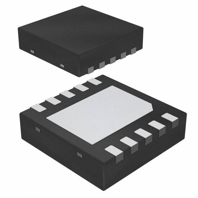
| 供应商器件封装 | 10-WSON (3x3) |
| 其它名称 | 296-29436-6 |
| 包装 | Digi-Reel® |
| 安装类型 | 表面贴装 |
| 封装/外壳 | 10-WFDFN 裸露焊盘 |
| 工作温度 | -40°C ~ 85°C |
| 接口 | - |
| 数字或字符 | - |
| 显示类型 | AMOLED |
| 标准包装 | 1 |
| 电压-电源 | 2.3 V ~ 5.5 V |
| 电流-电源 | 400µA |
| 配置 | 显示矩阵 |


PDF Datasheet 数据手册内容提取
TPS65137AS www.ti.com SLVSB21B–AUGUST2011–REVISEDSEPTEMBER2013 250mA Dual Outputs AMOLED Display Power Supply CheckforSamples:TPS65137AS FEATURES DESCRIPTION 1 • 2.5Vto4.8VInputVoltageRange The TPS65137AS is designed to drive AMOLED displays (Active Matrix Organic Light Emitting Diode) • 0.8%OutputVoltageAccuracyV POS requiring positive and negative voltage supply rails. • ExcellentLineTransientRegulation The device integrates a boost converter with LDO • 250mAOutputCurrent post regulator and an inverting buckboost converter suitable for battery operated products. The digital • Fixed4.6VV OutputVoltage POS control pin (CTRL) allows programming the negative • DigitallyProgrammableVNEG,–2.2Vto –5.2V output voltage in digital steps. The TPS65137AS • –4.9VDefaultValueforV uses a novel technology enabling excellent line and NEG load regulation. This is required to avoid disturbance • ShortCircuitProtection of the AMOLED display by the input voltage • ThermalShutdown disturbances occurring during transmit periods in • 3mm×3mm10-PinQFNPackage mobilephones. APPLICATIONS • ActiveMatrixOLED TYPICAL APPLICATION L1 4.7uH V V POS IN 4.6V/250mA 2.5V to 4.8V VIN TPS65137AS SWP C2 4.7PF C1 PGND OUTP 4.7PF V CTRL OUTN NEG EN and -4.9V/250mA Program V CT CB NEG C3 GND SWN C5 4.7PF C4 4.7PF 100nF L2 4.7PH 1 Pleasebeawarethatanimportantnoticeconcerningavailability,standardwarranty,anduseincriticalapplicationsof TexasInstrumentssemiconductorproductsanddisclaimerstheretoappearsattheendofthisdatasheet. PRODUCTIONDATAinformationiscurrentasofpublicationdate. Copyright©2011–2013,TexasInstrumentsIncorporated Products conform to specifications per the terms of the Texas Instruments standard warranty. Production processing does not necessarilyincludetestingofallparameters.
TPS65137AS SLVSB21B–AUGUST2011–REVISEDSEPTEMBER2013 www.ti.com This integrated circuit can be damaged by ESD. Texas Instruments recommends that all integrated circuits be handled with appropriateprecautions.Failuretoobserveproperhandlingandinstallationprocedurescancausedamage. ESDdamagecanrangefromsubtleperformancedegradationtocompletedevicefailure.Precisionintegratedcircuitsmaybemore susceptibletodamagebecauseverysmallparametricchangescouldcausethedevicenottomeetitspublishedspecifications. ORDERINGINFORMATION(1) (2) T PACKAGE(2) ORDERABLEPART TOP-SIDEMARKING A NUMBER –40°Cto85°C 10-Pin3x3QFN TPS65137ASDSCR PPGC (1) Forthemostcurrentpackageandorderinginformation,seethePackageOptionAddendumattheendofthisdocument,orseetheTI websiteatwww.ti.com. (2) Packagedrawings,thermaldata,andsymbolizationareavailableatwww.ti.com/packaging. ABSOLUTE MAXIMUM RATINGS overoperatingfree-airtemperaturerange(unlessotherwisenoted)(1) VALUE UNIT MIN MAX PVIN,SWP,OUTP,CTRL,VL,CB 5.5 V OUTN –6.5 V PinVoltage(2) SWN –6.5 5.5 V CT 3.6 V HBM 2 kV ESDrating MM 200 V CDM 500 V T Operatingjunctiontemperaturerange –40 50 °C J T Operatingambienttemperaturerange –40 85 °C A T Storagetemperaturerange –65 150 °C stg (1) Stressesbeyondthoselistedunderabsolutemaximumratingsmaycausepermanentdamagetothedevice.Thesearestressratings only,andfunctionaloperationofthedeviceattheseoranyotherconditionsbeyondthoseindicatedunderrecommendedoperating conditionsisnotimplied.Exposuretoabsolute–maximum–ratedconditionsforextendedperiodsmayaffectdevicereliability. (2) WithrespecttoGNDpin. THERMAL INFORMATION TPS65137AS THERMALMETRIC(1) DSC UNITS 10 θ Junction-to-ambientthermalresistance 56.5 JA θ Junction-to-boardthermalresistance 25.2 JB °C/W ψ Junction-to-topcharacterizationparameter 1.0 JT ψ Junction-to-boardcharacterizationparameter 17.9 JB (1) Formoreinformationabouttraditionalandnewthermalmetrics,seetheICPackageThermalMetricsapplicationreport,SPRA953. RECOMMENDED OPERATING CONDITIONS MIN TYP MAX UNIT V Inputsupplyvoltagerange 2.5 3.7 4.8 V IN T Operatingambienttemperature –40 25 85 °C A T Operatingjunctiontemperature –40 85 125 °C J 2 SubmitDocumentationFeedback Copyright©2011–2013,TexasInstrumentsIncorporated ProductFolderLinks:TPS65137AS
TPS65137AS www.ti.com SLVSB21B–AUGUST2011–REVISEDSEPTEMBER2013 ELECTRICAL CHARACTERISTICS V =3.7V,CTRL=V ,V =4.6V,V =–4.9V,T =–40°Cto85°C,typicalvaluesareatT =25°C(unlessotherwise IN IN POS NEG A A noted) PARAMETER TESTCONDITIONS MIN TYP MAX UNIT SUPPLYCURRENTANDTHERMALPROTECTION V Inputvoltagerange 2.5 4.8 V IN I OperatingquiescentcurrentintoV V andV havenoload(1) 16 mA Q IN POS NEG I ShutdowncurrentintoV CTRL=GND 0.1 μA SD IN V falling 2.0 IN V Under-voltagelockoutthreshold V UVLO V rising 2.3 IN Thermalshutdown 145 °C OUTPUTV POS V Positiveoutputvoltageregulation –0.8% 4.6 0.8% V POS SWPMOSFETon-resistance I =200mA 200 mΩ SWP r DS(ON) SWPMOSFETrectifieron-resistance I =200mA 250 mΩ SWP f SWPSwitchingfrequency I =0mA 1.6 MHz SWP POS I SWPswitchcurrentlimit Inductorvalleycurrent 0.9 1.2 A SWP V Shortcircuitthresholdinoperation V falling 3.7 V P(SCP) POS I LeakagecurrentintoV CTRL=GND 2 5 µA PLEAK POS V LDOdropoutvoltage I =100mA 400 mV DROP POS Lineregulation I =0mA 0 %/V POS Loadregulation I =0to250mA 0.28 %/A POS OUTPUTV NEG V Negativeoutputvoltagedefault –4.9 V NEG Negativeoutputvoltagerange –2.2 –5.2 V Negativeoutputvoltageregulation –5.2≤V ≤–4.2 –1% 1% NEG –4.2<V ≤–2.2 –1.5% 1.5% NEG SWNMOSFETon-resistance I =200mA 200 SWN r mΩ DS(ON) SWNMOSFETrectifieron-resistance I =200mA 300 SWN f SWNswitchingfrequency I =100mA 1.7 MHz SWN NEG I SWNswitchcurrentlimit V =2.9V 1.2 2.2 A SWN IN V Shortcircuitthresholdinoperation VoltagedropfromprogrammedV 420 mV N(SCP) NEG Shortcircuitthresholdinstart-up 0.18 0.21 0.24 V t Shortcircuitdetectiontimeinstart-up 10 ms N(SCP) I LeakagecurrentoutofV CTRL=GND 2 5 µA NLEAK NEG R V Pulldownresistorbeforestartup I =1mA 300 Ω N(PD) NEG NEG Lineregulation 0 %/V Loadregulation I =0to250mA 0.28 %/A NEG CTRLINTERFACE V Logichigh-levelvoltage 1.2 V H V Logiclow-levelvoltage 0.4 V L R Pulldownresistor 150 400 860 kΩ t Initializationtime 300 400 μs INIT t Shutdowntimeperiod 30 80 μs OFF t Pulsehighleveltimeperiod 2 10 25 μs HIGH t Pulselowleveltimeperiod 2 10 25 μs low t Datastorage/accepttimeperiod 30 80 μs STORE R C pinoutputimpedance 150 325 500 kΩ T T (1) WithinductorDFE252012C4.7µHfromTOKO Copyright©2011–2013,TexasInstrumentsIncorporated SubmitDocumentationFeedback 3 ProductFolderLinks:TPS65137AS
TPS65137AS SLVSB21B–AUGUST2011–REVISEDSEPTEMBER2013 www.ti.com DEVICE INFORMATION 10PINTQFNPACKAGE (TOPVIEW VIN 1 10 PGND SWN 2 9 SWP OUTN 3 Exposed 8 CB Thermal Die* CTRL 4 7 OUTP CT 5 6 GND PinFunctions PIN I/O(1) DESCRIPTION NO. NAME 1 VIN I Inputsupplyforthenegativebuck-boostconvertergeneratingV NEG 2 SWN I Switchpinofthenegativebuck-boostconverter 3 OUTN O Outputofnegativebuck-boostconverter 4 CTRL I CombinedenableandV programmingpin. NEG 5 CT O SetsthesettlingtimeforthevoltageonV whenprogrammedtoanewvalue NEG 6 GND G Analogground 7 OUTP O Outputoftheboostconverter 8 CB O Internalboostconverterbypasscapacitor 9 SWP I Switchpinoftheboostconverter 10 PGND G Powergroundofboostconverter Exposedthermaldie G ConnectthispadtoanalogGND. (1) G=Ground,I=Input,O=Output 4 SubmitDocumentationFeedback Copyright©2011–2013,TexasInstrumentsIncorporated ProductFolderLinks:TPS65137AS
TPS65137AS www.ti.com SLVSB21B–AUGUST2011–REVISEDSEPTEMBER2013 FUNCTIONAL BLOCK DIAGRAM SWP CB 9 8 OUTP LDO 7 Softstart SS Gate Drive generation SS Current SS PGND Short Circuit Sense/ Protection Softstart + SWP PWM + Control Vref SS Current Sense/ Short Circuit Softstart Protection OUTN PWM + CT Control + 5 5 Bit DAC Gate Drive Digital Interface VIN OUTN 1 3 6 2 4 10 GND SWN CTRL PGND Copyright©2011–2013,TexasInstrumentsIncorporated SubmitDocumentationFeedback 5 ProductFolderLinks:TPS65137AS
TPS65137AS SLVSB21B–AUGUST2011–REVISEDSEPTEMBER2013 www.ti.com TYPICAL CHARACTERISTICS TABLEOFGRAPHS FIGURE EfficiencyversusOutputcurrent(Outputcurrentis V =4.6V,V =–4.9V Figure1 fromV toV ) POS NEG POS NEG Startup Figure2 I =100mA,BoostandBuckBoost Figure3 OUT Switchpinsandoutputwaveforms(Outputcurrentis IOUT=250mA,BoostandBuckBoost Figure4 fromVPOStoVNEG) IOUT=250mA,Boost Figure5 I =250mA,BuckBoost Figure6 OUT EFFICIENCY vs OUTPUTCURRENT(V 4.6V,V -4.9V) STARTUP POS NEG 100 90 CTRL 5 V/div 80 70 VIN = 4.5V VPOS VIN = 3.7V 5 V/div % 60 VIN = 3.3V V Efficiency - 4500 VVIINN == 22..95VV 5 V/NdEiGv 30 20 10 Inductor IIN TOKO DFE252012C 4.7PH 200 mA/div 0 0.00 0.05 0.10 0.15 0.20 0.25 Output current - A 2 ms/div Figure1. Figure2. SWITCHPINSANDOUTPUTSBOOSTANDBUCKBOOST, SWITCHPINSANDOUTPUTSBOOSTANDBUCKBOOST, I 100mA I 250mA OUT OUT VPOS VPOS 50 mV/div 50 mV/div SWBOOST SWBOOST 5 V/div 5 V/div VNEG VNEG 50 mV/div 50 mV/div SWBUCKBOOST SWBUCKBOOST 5 V/div 5 V/div 500 ns/div 500 ns/div Figure3. Figure4. 6 SubmitDocumentationFeedback Copyright©2011–2013,TexasInstrumentsIncorporated ProductFolderLinks:TPS65137AS
TPS65137AS www.ti.com SLVSB21B–AUGUST2011–REVISEDSEPTEMBER2013 SWITCHPINSANDOUTPUTSBOOST,I 250mA SWITCHPINSANDOUTPUTSBUCKBOOST,I 250mA OUT OUT V POS 50 mV/div V NEG 50 mV/div SW BUCKBOOST 5 V/div SW BOOST 5 V/div I I L_BUCKBOOST L_BOOST 500 ma/div 200 ma/div 500 ns/div 500 ns/div Figure5. Figure6. Copyright©2011–2013,TexasInstrumentsIncorporated SubmitDocumentationFeedback 7 ProductFolderLinks:TPS65137AS
TPS65137AS SLVSB21B–AUGUST2011–REVISEDSEPTEMBER2013 www.ti.com APPLICATION FOR TYPICAL CHARACTERISTICS L1 4.7uH V V POS IN 4.6V/250mA 2.5V to 4.8V VIN TPS65137AS SWP C2 4.7PF C1 PGND OUTP 4.7PF V CTRL OUTN NEG EN and -4.9V/250mA Program V CT CB NEG C3 GND SWN C5 4.7PF C4 4.7PF 100nF L2 4.7PH Figure7. ApplicationforTypicalCharacteristics Table1.BillofMaterialsforTypicalCharacteristics Value PartNumber Manufacturer C1,C2,C3,C5 4.7µF,X5R GRM21BR61C475KA88 Murata C4 100nF,X7R GRM21BR71E104KA01 Murata L1,L2 4.7µH DFE252012C4.7µH TOKO 8 SubmitDocumentationFeedback Copyright©2011–2013,TexasInstrumentsIncorporated ProductFolderLinks:TPS65137AS
TPS65137AS www.ti.com SLVSB21B–AUGUST2011–REVISEDSEPTEMBER2013 DETAILED DESCRIPTION The TPS65137AS consists of a boost converter using an LDO as post regulator and an inverting buck-boost converter. The positive output is fixed at 4.6V. The negative output is programmable by a digital interface in the range of –2.2V to –5.2V, the default is –4.9V. The transition time of the negative output is adjustable by the CT pincapacitor. SOFT START and START-UP SEQUENCE The device has a soft start to limit the in-rush current. When the device is enabled by the CTRL pin going HIGH, the boost converter starts with a reduced switch current limit. 8ms after CTRL going HIGH, the buck-boost converterstartswiththedefaultvalueof –4.9V.Thetypicalstart-upsequenceisshowninFigure8. V POS CTRL 10ms Typ. V NEG Figure8. Start-upSequence SHORT CIRCUIT PROTECTION The device is protected against short circuits of the outputs to ground and short circuit of the outputs to each other. During normal operation, an error condition is detected if V falls below 3.7V for more than 3ms or V POS NEG gets above 420mV above the programmed value for more than 3ms. In either case, the device goes into shutdown and this state is latched. The input and the outputs are disconnected. To resume normal operation, V IN hastocyclebelowUVLOorCTRLhastotoggleLOWandHIGH. Duringstartup,anerrorconditionisdetectedinthefollowingcases: • V isnotinregulation10msafterCTRLgoesHIGH. POS • V ishigherthanthresholdlevel10msafterCTRLgoesHIGH. NEG • V isnotinregulation20msafterCTRLgoesHIGH. NEG In the above cases, the device goes into shutdown and this state is latched. The input and the outputs are disconnected. To resume normal operation, VIN has to cycle below UVLO or CTRL has to toggle LOW and HIGH. ENABLE (CTRL PIN) The CTRL pin serves two functions. One is to enable and disable the device the other is the output voltage programming of the device. If the digital interface is not required the CTRL pin can be used as a standard enable pinforthedeviceandthedevicewillcomeupwithitsdefaultvalueonV of–4.9V.WhenCTRLispulledhigh, NEG thedeviceisenabled.ThedeviceisshutdownwithCTRLlow. DIGITAL INTERFACE (CTRL) The digital interface allows programming the negative output voltage V in digital steps. If the digital output NEG voltagesettingisnotrequiredthentheCTRLpincanalsobeusedasastandardenablepin. Copyright©2011–2013,TexasInstrumentsIncorporated SubmitDocumentationFeedback 9 ProductFolderLinks:TPS65137AS
TPS65137AS SLVSB21B–AUGUST2011–REVISEDSEPTEMBER2013 www.ti.com The digital output voltage programming of V is implemented by a simple digital interface with the timing NEG showninFigure9. tINIT tLOW tHIGH tSTORE tOFF High CTRL Low 4.62V V POS t SCP t SET V NEG -4.9V -5.0V Figure9. DigitalInterfaceUsingCTRL Once CTRL is pulled high the device will come up with its default voltage of –4.9V. The device has a 6-bit DAC implemented with the corresponding output voltages as given in the table below. The interface counts now the risingedgesappliedtotheCTRLpinoncethedeviceisenabled.Fortheexampleabove,V isprogrammedto NEG –5.0Vsince3risingedgesaredetected.OtheroutputvoltagescanbeprogrammedaccordingTable2. Table2.ProgrammingTableforV NEG BIT/RISINGEDGES V DACVALUE BIT/RISINGEDGES V DACVALUE NEG NEG 0/nopulse –4.9V 00000 16 –3.7V 10000 1 –5.2V 00001 17 –3.6V 10001 2 –5.1V 00010 18 –3.5V 10010 3 –5.0V 00011 19 –3.4V 10011 4 –4.9V 00100 20 –3.3V 10100 5 –4.8V 00101 21 –3.2V 10101 6 –4.7V 00110 22 –3.1V 10110 7 –4.6V 00111 23 –3.0V 10111 8 –4.5V 01000 24 –2.9V 11000 9 –4.4V 01001 25 –2.8V 11001 10 –4.3V 01010 26 –2.7V 11010 11 –4.2V 01011 27 –2.6V 11011 12 –4.1V 01100 28 –2.5V 11100 13 –4.0V 01101 29 –2.4V 11101 14 –3.9V 01110 30 –2.3V 11110 15 –3.8V 01111 31 –2.2V 11111 10 SubmitDocumentationFeedback Copyright©2011–2013,TexasInstrumentsIncorporated ProductFolderLinks:TPS65137AS
TPS65137AS www.ti.com SLVSB21B–AUGUST2011–REVISEDSEPTEMBER2013 SETTINGTRANSITIONTIMEt forV (C ) set NEG T The device allows setting the transition time t using an external capacitor connected to pin CT. The transition set time is the time period required to move V from one voltage level to the next programmed voltage level. The NEG capacitor connected to pin CT does not influence the soft start time t of the V default value. When the CT ss NEG pin is left open then the shortest possible transition time is programmed. When connecting a capacitor to the CT pinthenthetransitiontimeisgivenbyanR-Ctimeconstant.ThisisgivenbytheoutputimpedanceoftheCTpin typically 325kΩ and the external capacitance. Within one τ the output voltage V has reached 70% of its NEG programmedvalue.Anexampleisgivenwhenusing100nFforC . T τ≈ t =325kΩ ×C =325kΩ × 100nF=32.5mS set70% T Theoutputvoltageisalmostatitsprogrammedvalueafter3τ. PCB LAYOUT Figure10andFigure11showanexampleofaPCBlayoutdesign. 1. PlacetheinputcapacitoronVINandtheoutputcapacitoronOUTNascloseaspossibletothedevice. UseshortandwidetracestoconnecttheinputcapacitortoVINandtheoutputcapacitortoOUTN. 2. PlacetheoutputcapacitoronOUTPandthecapacitoronCBascloseaspossibletothedevice. UseshortandwidetracestoconnecttheoutputcapacitortoOUTP. 3. ConnectthegroundoftheCTcapacitortotheGNDpin,pin6,directly. 4. Connecttheinputgroundandtheoutputgroundonthesameboardlayer,notthroughvias. Figure10. ExampleofPCBLayoutDesign(Toplayer) Copyright©2011–2013,TexasInstrumentsIncorporated SubmitDocumentationFeedback 11 ProductFolderLinks:TPS65137AS
TPS65137AS SLVSB21B–AUGUST2011–REVISEDSEPTEMBER2013 www.ti.com Figure11. ExampleofPCBLayoutDesign(Bottomlayer) Figure12. SchematicfortheExampleofPCBLayoutDesign 12 SubmitDocumentationFeedback Copyright©2011–2013,TexasInstrumentsIncorporated ProductFolderLinks:TPS65137AS
TPS65137AS www.ti.com SLVSB21B–AUGUST2011–REVISEDSEPTEMBER2013 L1 4.7uH V V POS IN 4.6V/250mA 2.5V to 4.8V VIN TPS65137AS SWP C2 4.7PF C1 PGND OUTP 4.7PF V CTRL OUTN NEG EN and -4.9V/250mA Program V CT CB NEG C3 GND SWN C5 4.7PF C4 4.7PF 100nF L2 4.7PH Figure13. TypicalApplicationCircuit Copyright©2011–2013,TexasInstrumentsIncorporated SubmitDocumentationFeedback 13 ProductFolderLinks:TPS65137AS
PACKAGE OPTION ADDENDUM www.ti.com 6-Feb-2020 PACKAGING INFORMATION Orderable Device Status Package Type Package Pins Package Eco Plan Lead/Ball Finish MSL Peak Temp Op Temp (°C) Device Marking Samples (1) Drawing Qty (2) (6) (3) (4/5) TPS65137ASDSCR ACTIVE WSON DSC 10 3000 Green (RoHS NIPDAU Level-2-260C-1 YEAR -40 to 85 PPGC & no Sb/Br) (1) The marketing status values are defined as follows: ACTIVE: Product device recommended for new designs. LIFEBUY: TI has announced that the device will be discontinued, and a lifetime-buy period is in effect. NRND: Not recommended for new designs. Device is in production to support existing customers, but TI does not recommend using this part in a new design. PREVIEW: Device has been announced but is not in production. Samples may or may not be available. OBSOLETE: TI has discontinued the production of the device. (2) RoHS: TI defines "RoHS" to mean semiconductor products that are compliant with the current EU RoHS requirements for all 10 RoHS substances, including the requirement that RoHS substance do not exceed 0.1% by weight in homogeneous materials. Where designed to be soldered at high temperatures, "RoHS" products are suitable for use in specified lead-free processes. TI may reference these types of products as "Pb-Free". RoHS Exempt: TI defines "RoHS Exempt" to mean products that contain lead but are compliant with EU RoHS pursuant to a specific EU RoHS exemption. Green: TI defines "Green" to mean the content of Chlorine (Cl) and Bromine (Br) based flame retardants meet JS709B low halogen requirements of <=1000ppm threshold. Antimony trioxide based flame retardants must also meet the <=1000ppm threshold requirement. (3) MSL, Peak Temp. - The Moisture Sensitivity Level rating according to the JEDEC industry standard classifications, and peak solder temperature. (4) There may be additional marking, which relates to the logo, the lot trace code information, or the environmental category on the device. (5) Multiple Device Markings will be inside parentheses. Only one Device Marking contained in parentheses and separated by a "~" will appear on a device. If a line is indented then it is a continuation of the previous line and the two combined represent the entire Device Marking for that device. (6) Lead/Ball Finish - Orderable Devices may have multiple material finish options. Finish options are separated by a vertical ruled line. Lead/Ball Finish values may wrap to two lines if the finish value exceeds the maximum column width. Important Information and Disclaimer:The information provided on this page represents TI's knowledge and belief as of the date that it is provided. TI bases its knowledge and belief on information provided by third parties, and makes no representation or warranty as to the accuracy of such information. Efforts are underway to better integrate information from third parties. TI has taken and continues to take reasonable steps to provide representative and accurate information but may not have conducted destructive testing or chemical analysis on incoming materials and chemicals. TI and TI suppliers consider certain information to be proprietary, and thus CAS numbers and other limited information may not be available for release. In no event shall TI's liability arising out of such information exceed the total purchase price of the TI part(s) at issue in this document sold by TI to Customer on an annual basis. Addendum-Page 1
PACKAGE MATERIALS INFORMATION www.ti.com 5-Sep-2013 TAPE AND REEL INFORMATION *Alldimensionsarenominal Device Package Package Pins SPQ Reel Reel A0 B0 K0 P1 W Pin1 Type Drawing Diameter Width (mm) (mm) (mm) (mm) (mm) Quadrant (mm) W1(mm) TPS65137ASDSCR WSON DSC 10 3000 330.0 12.4 3.3 3.3 1.1 8.0 12.0 Q2 TPS65137ASDSCR WSON DSC 10 3000 330.0 12.4 3.3 3.3 1.1 8.0 12.0 Q2 PackMaterials-Page1
PACKAGE MATERIALS INFORMATION www.ti.com 5-Sep-2013 *Alldimensionsarenominal Device PackageType PackageDrawing Pins SPQ Length(mm) Width(mm) Height(mm) TPS65137ASDSCR WSON DSC 10 3000 552.0 367.0 36.0 TPS65137ASDSCR WSON DSC 10 3000 367.0 367.0 35.0 PackMaterials-Page2
None
PACKAGE OUTLINE DSC0010J WSON - 0.8 mm max height SCALE 4.000 PLASTIC SMALL OUTLINE - NO LEAD 3.1 B A 2.9 PIN 1 INDEX AREA 3.1 2.9 0.8 C 0.7 SEATING PLANE 0.05 0.00 0.08 C 1.65 0.1 2X (0.5) (0.2) TYP EXPOSED 4X (0.25) THERMAL PAD 5 6 2X 11 SYMM 2 2.4 0.1 10 1 8X 0.5 0.30 10X 0.18 PIN 1 ID SYMM 0.1 C A B (OPTIONAL) 0.5 0.05 C 10X 0.3 4221826/D 08/2018 NOTES: 1. All linear dimensions are in millimeters. Any dimensions in parenthesis are for reference only. Dimensioning and tolerancing per ASME Y14.5M. 2. This drawing is subject to change without notice. 3. The package thermal pad must be soldered to the printed circuit board for optimal thermal and mechanical performance. www.ti.com
EXAMPLE BOARD LAYOUT DSC0010J WSON - 0.8 mm max height PLASTIC SMALL OUTLINE - NO LEAD (1.65) (0.5) 10X (0.6) 1 10 10X (0.24) 11 SYMM (2.4) (3.4) (0.95) 8X (0.5) 6 5 (R0.05) TYP ( 0.2) VIA TYP (0.25) (0.575) SYMM (2.8) LAND PATTERN EXAMPLE EXPOSED METAL SHOWN SCALE:20X 0.07 MIN 0.07 MAX EXPOSED METAL ALL AROUND ALL AROUND EXPOSED METAL SOLDER MASK METAL METAL UNDER SOLDER MASK OPENING SOLDER MASK OPENING NON SOLDER MASK SOLDER MASK DEFINED DEFINED (PREFERRED) SOLDER MASK DETAILS 4221826/D 08/2018 NOTES: (continued) 4. This package is designed to be soldered to a thermal pad on the board. For more information, see Texas Instruments literature number SLUA271 (www.ti.com/lit/slua271). 5. Vias are optional depending on application, refer to device data sheet. If any vias are implemented, refer to their locations shown on this view. It is recommended that vias under paste be filled, plugged or tented. www.ti.com
EXAMPLE STENCIL DESIGN DSC0010J WSON - 0.8 mm max height PLASTIC SMALL OUTLINE - NO LEAD 2X (1.5) (0.5) SYMM EXPOSED METAL 11 TYP 10X (0.6) 1 10 (1.53) 10X (0.24) 2X (1.06) SYMM (0.63) 8X (0.5) 6 5 (R0.05) TYP 4X (0.34) 4X (0.25) (2.8) SOLDER PASTE EXAMPLE BASED ON 0.125 mm THICK STENCIL EXPOSED PAD 11: 80% PRINTED SOLDER COVERAGE BY AREA SCALE:25X 4221826/D 08/2018 NOTES: (continued) 6. Laser cutting apertures with trapezoidal walls and rounded corners may offer better paste release. IPC-7525 may have alternate design recommendations. www.ti.com
IMPORTANTNOTICEANDDISCLAIMER TI PROVIDES TECHNICAL AND RELIABILITY DATA (INCLUDING DATASHEETS), DESIGN RESOURCES (INCLUDING REFERENCE DESIGNS), APPLICATION OR OTHER DESIGN ADVICE, WEB TOOLS, SAFETY INFORMATION, AND OTHER RESOURCES “AS IS” AND WITH ALL FAULTS, AND DISCLAIMS ALL WARRANTIES, EXPRESS AND IMPLIED, INCLUDING WITHOUT LIMITATION ANY IMPLIED WARRANTIES OF MERCHANTABILITY, FITNESS FOR A PARTICULAR PURPOSE OR NON-INFRINGEMENT OF THIRD PARTY INTELLECTUAL PROPERTY RIGHTS. These resources are intended for skilled developers designing with TI products. You are solely responsible for (1) selecting the appropriate TI products for your application, (2) designing, validating and testing your application, and (3) ensuring your application meets applicable standards, and any other safety, security, or other requirements. These resources are subject to change without notice. TI grants you permission to use these resources only for development of an application that uses the TI products described in the resource. Other reproduction and display of these resources is prohibited. No license is granted to any other TI intellectual property right or to any third party intellectual property right. TI disclaims responsibility for, and you will fully indemnify TI and its representatives against, any claims, damages, costs, losses, and liabilities arising out of your use of these resources. TI’s products are provided subject to TI’s Terms of Sale (www.ti.com/legal/termsofsale.html) or other applicable terms available either on ti.com or provided in conjunction with such TI products. TI’s provision of these resources does not expand or otherwise alter TI’s applicable warranties or warranty disclaimers for TI products. Mailing Address: Texas Instruments, Post Office Box 655303, Dallas, Texas 75265 Copyright © 2020, Texas Instruments Incorporated