ICGOO在线商城 > 集成电路(IC) > PMIC - 显示器驱动器 > PCF8545ATT/AJ

 Datasheet下载
- 型号: PCF8545ATT/AJ
- 制造商: NXP Semiconductors
- 库位|库存: xxxx|xxxx
- 要求:
| 数量阶梯 | 香港交货 | 国内含税 |
| +xxxx | $xxxx | ¥xxxx |
查看当月历史价格
查看今年历史价格
PCF8545ATT/AJ产品简介:
ICGOO电子元器件商城为您提供PCF8545ATT/AJ由NXP Semiconductors设计生产,在icgoo商城现货销售,并且可以通过原厂、代理商等渠道进行代购。 PCF8545ATT/AJ价格参考。NXP SemiconductorsPCF8545ATT/AJ封装/规格:PMIC - 显示器驱动器, 。您可以下载PCF8545ATT/AJ参考资料、Datasheet数据手册功能说明书,资料中有PCF8545ATT/AJ 详细功能的应用电路图电压和使用方法及教程。
NXP USA Inc.的PMIC(电源管理集成电路)型号PCF8545ATT/AJ属于显示器驱动器类别,主要用于小型液晶显示器(LCD)的驱动控制。该芯片支持段码式LCD驱动,适用于低功耗、小型化的电子产品。

其典型应用场景包括:

1. 便携式消费电子产品:如电子秤、计算器、电子词典、手持式测量仪器等,这些设备通常使用小型LCD屏,要求低功耗和高集成度。

2. 家电控制面板:微波炉、洗衣机、电饭煲等家用电器的显示界面,用于驱动段码LCD,显示时间、温度、状态等信息。

3. 工业仪表与控制设备:用于温度控制器、压力传感器、电能表等工业设备的显示模块,提供清晰、稳定的显示效果。

4. 汽车电子:如车载仪表、倒车雷达显示、车载充电器等,适用于对稳定性和可靠性要求较高的环境。

5. 医疗设备:如血糖仪、血压计、便携式监护仪等,用于显示测量数据,满足医疗设备对精度和低功耗的需求。

PCF8545ATT/AJ采用I²C总线接口,便于与微控制器连接,支持多种偏置电压配置,适用于不同类型的LCD面板。其封装形式为TSSOP,适合高密度PCB布局。
| 参数 | 数值 |
| 产品目录 | 集成电路 (IC) |
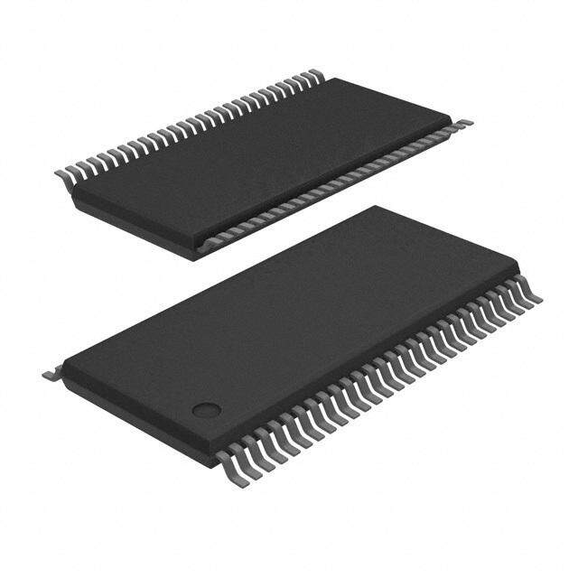
| 描述 | IC LCD DRIVER UNIV 56TSSOP |
| 产品分类 | |
| 品牌 | NXP Semiconductors |
| 数据手册 | |
| 产品图片 | |
| 产品型号 | PCF8545ATT/AJ |
| rohs | 无铅 / 符合限制有害物质指令(RoHS)规范要求 |
| 产品系列 | - |
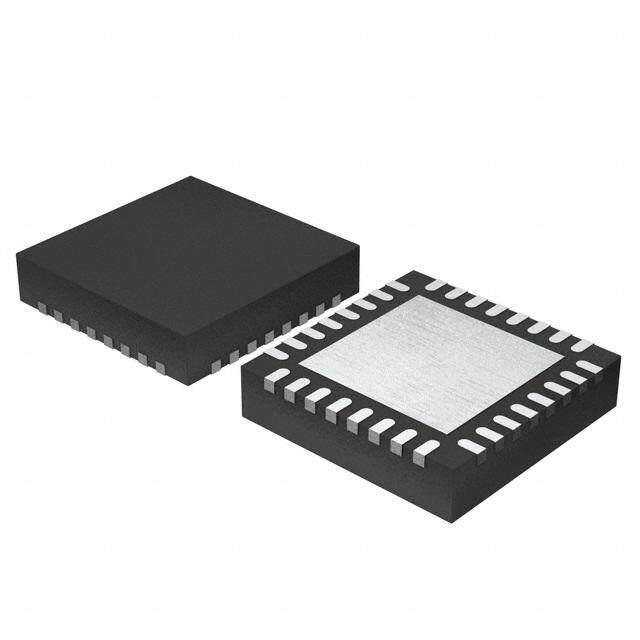
| 供应商器件封装 | 56-TSSOP |
| 其它名称 | 568-10998-6 |
| 包装 | Digi-Reel® |
| 安装类型 | 表面贴装 |
| 封装/外壳 | 56-TFSOP(0.240",6.10mm 宽) |
| 工作温度 | -40°C ~ 95°C |
| 接口 | I²C |
| 数字或字符 | - |
| 显示类型 | LCD |
| 标准包装 | 1 |
| 电压-电源 | 1.8 V ~ 5.5 V |
| 电流-电源 | 30µA |
| 配置 | 320 段 |


- 商务部:美国ITC正式对集成电路等产品启动337调查
- 曝三星4nm工艺存在良率问题 高通将骁龙8 Gen1或转产台积电
- 太阳诱电将投资9.5亿元在常州建新厂生产MLCC 预计2023年完工
- 英特尔发布欧洲新工厂建设计划 深化IDM 2.0 战略
- 台积电先进制程称霸业界 有大客户加持明年业绩稳了
- 达到5530亿美元!SIA预计今年全球半导体销售额将创下新高
- 英特尔拟将自动驾驶子公司Mobileye上市 估值或超500亿美元
- 三星加码芯片和SET,合并消费电子和移动部门,撤换高东真等 CEO
- 三星电子宣布重大人事变动 还合并消费电子和移动部门
- 海关总署:前11个月进口集成电路产品价值2.52万亿元 增长14.8%


PDF Datasheet 数据手册内容提取
PCF8545 Universal LCD driver for multiplex rates up to 1:8 Rev. 1 — 13 November 2013 Product data sheet 1. General description The PCF8545 is a peripheral device which interfaces to almost any Liquid Crystal Display (LCD)1 with low multiplex rates. It generates the drive signals for any multiplexed LCD containing up to eight backplanes, and up to 320 elements. The PCF8545 is compatible with most microcontrollers and communicates via the two-line bidirectional I2C-bus (PCF8545A) or a three line unidirectional SPI-bus (PCF8545B). Communication overheads are minimized using a display RAM with auto-incremented addressing. For a selection of NXP LCD segment drivers, see Table40 on page61. 2. Features and benefits Single-chip 320 elements LCD controllerand driver Wide range for digital power supply: from 1.8Vto5.5V LCD supply range from 2.5V up to 5.5V LCD and logic supplies may be separated Low power consumption Selectable backplane drive configuration: 4, 6, or8 backplane multiplexing Selectable display bias configuration 320-bit RAM for display data storage 400kHz I2C-bus interface (PCF8545A) 5 MHz SPI-bus interface (PCF8545B) Programmable frame frequency in the range of 60Hz to 300Hz in steps of 10Hz; factory calibrated 320segments driven allowing: up to 40 7-segment alphanumeric characters up to 20 14-segment alphanumeric characters any graphics of up to 320elements Manufactured in silicon gate CMOS process 3. Applications Industrial and consumer products 1. The definition of the abbreviations and acronyms used in this data sheet can be found in Section21.
PCF8545 NXP Semiconductors Universal LCD driver for multiplex rates up to 1:8 4. Ordering information Table 1. Ordering information Type number Interface Package type Name Description Version PCF8545ATT I2C-bus TSSOP56 plastic thin shrink small outline SOT364-1 package; 56 leads; body width 6.1 mm PCF8545BTT SPI-bus TSSOP56 plastic thin shrink small outline SOT364-1 package; 56 leads; body width 6.1 mm 4.1 Ordering options Table 2. Ordering opt ions Product type number Sales item (12NC) Orderable part IC Delivery form number revision PCF8545ATT/A 935302987118 PCF8545ATT/AJ 1 tape and reel, 13 inch PCF8545BTT/A 935302988118 PCF8545BTT/AJ 1 tape and reel, 13 inch 5. Marking Table 3. Marking codes Type number Marking code PCF8545ATT/A PCF8545ATT PCF8545BTT/A PCF8545BTT PCF8545 All information provided in this document is subject to legal disclaimers. © NXP B.V. 2013. All rights reserved. Product data sheet Rev. 1 — 13 November 2013 2 of 72
PCF8545 NXP Semiconductors Universal LCD driver for multiplex rates up to 1:8 6. Block diagram (cid:37)(cid:51)(cid:23)(cid:3)(cid:87)(cid:82)(cid:3)(cid:37)(cid:51)(cid:26)(cid:18) (cid:57)(cid:39)(cid:39) (cid:37)(cid:51)(cid:19)(cid:3)(cid:87)(cid:82)(cid:3)(cid:37)(cid:51)(cid:22) (cid:54)(cid:23)(cid:19)(cid:3)(cid:87)(cid:82)(cid:3)(cid:54)(cid:23)(cid:22) (cid:54)(cid:19)(cid:3)(cid:87)(cid:82)(cid:3)(cid:54)(cid:22)(cid:28) (cid:57)(cid:47)(cid:38)(cid:39) (cid:37)(cid:36)(cid:38)(cid:46)(cid:51)(cid:47)(cid:36)(cid:49)(cid:40) (cid:39)(cid:44)(cid:54)(cid:51)(cid:47)(cid:36)(cid:60)(cid:3)(cid:54)(cid:40)(cid:42)(cid:48)(cid:40)(cid:49)(cid:55) (cid:47)(cid:38)(cid:39) (cid:50)(cid:56)(cid:55)(cid:51)(cid:56)(cid:55)(cid:54) (cid:50)(cid:56)(cid:55)(cid:51)(cid:56)(cid:55)(cid:54) (cid:57)(cid:50)(cid:47)(cid:55)(cid:36)(cid:42)(cid:40) (cid:54)(cid:40)(cid:47)(cid:40)(cid:38)(cid:55)(cid:50)(cid:53) (cid:39)(cid:44)(cid:54)(cid:51)(cid:47)(cid:36)(cid:60)(cid:3)(cid:53)(cid:40)(cid:42)(cid:44)(cid:54)(cid:55)(cid:40)(cid:53) (cid:47)(cid:38)(cid:39)(cid:3)(cid:37)(cid:44)(cid:36)(cid:54) (cid:42)(cid:40)(cid:49)(cid:40)(cid:53)(cid:36)(cid:55)(cid:50)(cid:53) (cid:57)(cid:54)(cid:54) (cid:39)(cid:44)(cid:54)(cid:51)(cid:47)(cid:36)(cid:60)(cid:3)(cid:53)(cid:36)(cid:48) (cid:50)(cid:54)(cid:38)(cid:44)(cid:47)(cid:47)(cid:36)(cid:55)(cid:50)(cid:53) (cid:51)(cid:38)(cid:41)(cid:27)(cid:24)(cid:23)(cid:24)(cid:36) (cid:51)(cid:53)(cid:40)(cid:54)(cid:38)(cid:36)(cid:47)(cid:40)(cid:53) (cid:50)(cid:54)(cid:38)(cid:38)(cid:47)(cid:46) (cid:36)(cid:49)(cid:39)(cid:3)(cid:38)(cid:47)(cid:50)(cid:38)(cid:46) (cid:36)(cid:49)(cid:39)(cid:3)(cid:55)(cid:44)(cid:48)(cid:44)(cid:49)(cid:42) (cid:54)(cid:40)(cid:47)(cid:40)(cid:38)(cid:55)(cid:44)(cid:50)(cid:49) (cid:51)(cid:50)(cid:58)(cid:40)(cid:53)(cid:16)(cid:50)(cid:49) (cid:38)(cid:50)(cid:48)(cid:48)(cid:36)(cid:49)(cid:39) (cid:58)(cid:53)(cid:44)(cid:55)(cid:40)(cid:3)(cid:39)(cid:36)(cid:55)(cid:36) (cid:39)(cid:36)(cid:55)(cid:36)(cid:3)(cid:51)(cid:50)(cid:44)(cid:49)(cid:55)(cid:40)(cid:53)(cid:15) (cid:53)(cid:40)(cid:54)(cid:40)(cid:55) (cid:53)(cid:40)(cid:54)(cid:40)(cid:55) (cid:39)(cid:40)(cid:38)(cid:50)(cid:39)(cid:40)(cid:53) (cid:38)(cid:50)(cid:49)(cid:55)(cid:53)(cid:50)(cid:47) (cid:36)(cid:56)(cid:55)(cid:50)(cid:3)(cid:44)(cid:49)(cid:38)(cid:53)(cid:40)(cid:48)(cid:40)(cid:49)(cid:55) (cid:54)(cid:38)(cid:47) (cid:44)(cid:49)(cid:51)(cid:56)(cid:55) (cid:44)(cid:21)(cid:38)(cid:16)(cid:37)(cid:56)(cid:54) (cid:54)(cid:39)(cid:36) (cid:41)(cid:44)(cid:47)(cid:55)(cid:40)(cid:53)(cid:54) (cid:38)(cid:50)(cid:49)(cid:55)(cid:53)(cid:50)(cid:47)(cid:47)(cid:40)(cid:53) (cid:68)(cid:68)(cid:68)(cid:16)(cid:19)(cid:19)(cid:27)(cid:22)(cid:20)(cid:28) (cid:36)(cid:19) Fig 1. Block diagram of PCF8545A PCF8545 All information provided in this document is subject to legal disclaimers. © NXP B.V. 2013. All rights reserved. Product data sheet Rev. 1 — 13 November 2013 3 of 72
PCF8545 NXP Semiconductors Universal LCD driver for multiplex rates up to 1:8 (cid:37)(cid:51)(cid:23)(cid:3)(cid:87)(cid:82)(cid:3)(cid:37)(cid:51)(cid:26)(cid:18) (cid:57)(cid:39)(cid:39) (cid:37)(cid:51)(cid:19)(cid:3)(cid:87)(cid:82)(cid:3)(cid:37)(cid:51)(cid:22) (cid:54)(cid:23)(cid:19)(cid:3)(cid:87)(cid:82)(cid:3)(cid:54)(cid:23)(cid:22) (cid:54)(cid:19)(cid:3)(cid:87)(cid:82)(cid:3)(cid:54)(cid:22)(cid:28) (cid:57)(cid:47)(cid:38)(cid:39) (cid:37)(cid:36)(cid:38)(cid:46)(cid:51)(cid:47)(cid:36)(cid:49)(cid:40) (cid:39)(cid:44)(cid:54)(cid:51)(cid:47)(cid:36)(cid:60)(cid:3)(cid:54)(cid:40)(cid:42)(cid:48)(cid:40)(cid:49)(cid:55) (cid:47)(cid:38)(cid:39) (cid:50)(cid:56)(cid:55)(cid:51)(cid:56)(cid:55)(cid:54) (cid:50)(cid:56)(cid:55)(cid:51)(cid:56)(cid:55)(cid:54) (cid:57)(cid:50)(cid:47)(cid:55)(cid:36)(cid:42)(cid:40) (cid:54)(cid:40)(cid:47)(cid:40)(cid:38)(cid:55)(cid:50)(cid:53) (cid:39)(cid:44)(cid:54)(cid:51)(cid:47)(cid:36)(cid:60)(cid:3)(cid:53)(cid:40)(cid:42)(cid:44)(cid:54)(cid:55)(cid:40)(cid:53) (cid:47)(cid:38)(cid:39)(cid:3)(cid:37)(cid:44)(cid:36)(cid:54) (cid:42)(cid:40)(cid:49)(cid:40)(cid:53)(cid:36)(cid:55)(cid:50)(cid:53) (cid:57)(cid:54)(cid:54) (cid:39)(cid:44)(cid:54)(cid:51)(cid:47)(cid:36)(cid:60)(cid:3)(cid:53)(cid:36)(cid:48) (cid:50)(cid:54)(cid:38)(cid:44)(cid:47)(cid:47)(cid:36)(cid:55)(cid:50)(cid:53) (cid:51)(cid:38)(cid:41)(cid:27)(cid:24)(cid:23)(cid:24)(cid:37) (cid:51)(cid:53)(cid:40)(cid:54)(cid:38)(cid:36)(cid:47)(cid:40)(cid:53) (cid:50)(cid:54)(cid:38)(cid:38)(cid:47)(cid:46) (cid:36)(cid:49)(cid:39)(cid:3)(cid:38)(cid:47)(cid:50)(cid:38)(cid:46) (cid:36)(cid:49)(cid:39)(cid:3)(cid:55)(cid:44)(cid:48)(cid:44)(cid:49)(cid:42) (cid:54)(cid:40)(cid:47)(cid:40)(cid:38)(cid:55)(cid:44)(cid:50)(cid:49) (cid:51)(cid:50)(cid:58)(cid:40)(cid:53)(cid:16)(cid:50)(cid:49) (cid:38)(cid:50)(cid:48)(cid:48)(cid:36)(cid:49)(cid:39) (cid:58)(cid:53)(cid:44)(cid:55)(cid:40)(cid:3)(cid:39)(cid:36)(cid:55)(cid:36) (cid:39)(cid:36)(cid:55)(cid:36)(cid:3)(cid:51)(cid:50)(cid:44)(cid:49)(cid:55)(cid:40)(cid:53)(cid:15) (cid:53)(cid:40)(cid:54)(cid:40)(cid:55) (cid:53)(cid:40)(cid:54)(cid:40)(cid:55) (cid:39)(cid:40)(cid:38)(cid:50)(cid:39)(cid:40)(cid:53) (cid:38)(cid:50)(cid:49)(cid:55)(cid:53)(cid:50)(cid:47) (cid:36)(cid:56)(cid:55)(cid:50)(cid:3)(cid:44)(cid:49)(cid:38)(cid:53)(cid:40)(cid:48)(cid:40)(cid:49)(cid:55) (cid:54)(cid:38)(cid:47) (cid:54)(cid:51)(cid:44)(cid:16)(cid:37)(cid:56)(cid:54) (cid:54)(cid:39)(cid:44) (cid:38)(cid:50)(cid:49)(cid:55)(cid:53)(cid:50)(cid:47)(cid:47)(cid:40)(cid:53) (cid:68)(cid:68)(cid:68)(cid:16)(cid:19)(cid:19)(cid:27)(cid:22)(cid:21)(cid:19) (cid:38)(cid:40) Fig 2. Block diagram of PCF8545B PCF8545 All information provided in this document is subject to legal disclaimers. © NXP B.V. 2013. All rights reserved. Product data sheet Rev. 1 — 13 November 2013 4 of 72
xxxxxxxxxxxxxxxxxxxxx xxxxxxxxxxxxxxxxxxxxxxxxxx xxxxxxx x x x xxxxxxxxxxxxxxxxxxxxxxxxxxxxxx xxxxxxxxxxxxxxxxxxx xx xx xxxxx xxxxxxxxxxxxxxxxxxxxxxxxxxx xxxxxxxxxxxxxxxxxxx xxxxxx xxxxxxxxxxxxxxxxxxxxxxxxxxxxxxxxxxx xxxxxxxxxxxx x x xxxxxxxxxxxxxxxxxxxxx xxxxxxxxxxxxxxxxxxxxxxxxxxxxxx xxxxx xxxxxxxxxxxxxxxxxxxxxxxxxxxxxxxxxxxxxxxxxxxxxxxxxx xxxxxxxx xxxxxxxxxxxxxxxxxxxxxxxxx xxxxxxxxxxxxxxxxxxxx xxx Produ PCF8545 7. Pinning information NXP ct d Se a 7.1 Pinning ta m s i h c e o e t n d (cid:54)(cid:28) (cid:20) (cid:24)(cid:25) (cid:54)(cid:27) (cid:54)(cid:28) (cid:20) (cid:24)(cid:25) (cid:54)(cid:27) u c (cid:54)(cid:20)(cid:19) (cid:21) (cid:24)(cid:24) (cid:54)(cid:26) (cid:54)(cid:20)(cid:19) (cid:21) (cid:24)(cid:24) (cid:54)(cid:26) t o (cid:54)(cid:20)(cid:20) (cid:22) (cid:24)(cid:23) (cid:54)(cid:25) (cid:54)(cid:20)(cid:20) (cid:22) (cid:24)(cid:23) (cid:54)(cid:25) r s (cid:54)(cid:20)(cid:21) (cid:23) (cid:24)(cid:22) (cid:54)(cid:24) (cid:54)(cid:20)(cid:21) (cid:23) (cid:24)(cid:22) (cid:54)(cid:24) (cid:54)(cid:20)(cid:22) (cid:24) (cid:24)(cid:21) (cid:54)(cid:23) (cid:54)(cid:20)(cid:22) (cid:24) (cid:24)(cid:21) (cid:54)(cid:23) (cid:54)(cid:20)(cid:23) (cid:25) (cid:24)(cid:20) (cid:54)(cid:22) (cid:54)(cid:20)(cid:23) (cid:25) (cid:24)(cid:20) (cid:54)(cid:22) (cid:54)(cid:20)(cid:24) (cid:26) (cid:24)(cid:19) (cid:54)(cid:21) (cid:54)(cid:20)(cid:24) (cid:26) (cid:24)(cid:19) (cid:54)(cid:21) A (cid:54)(cid:20)(cid:25) (cid:27) (cid:23)(cid:28) (cid:54)(cid:20) (cid:54)(cid:20)(cid:25) (cid:27) (cid:23)(cid:28) (cid:54)(cid:20) ll inform (cid:54)(cid:20)(cid:26) (cid:28) (cid:23)(cid:27) (cid:54)(cid:19) (cid:54)(cid:20)(cid:26) (cid:28) (cid:23)(cid:27) (cid:54)(cid:19) Rev. 1 — 13 No ation provided in this docum (cid:37)(cid:37)(cid:37)(cid:51)(cid:51)(cid:51)(cid:20)(cid:21)(cid:19)(cid:18)(cid:18)(cid:18)(cid:54)(cid:54)(cid:54)(cid:54)(cid:54)(cid:22)(cid:22)(cid:22)(cid:20)(cid:20)(cid:22)(cid:23)(cid:21)(cid:27)(cid:28) (cid:20)(cid:20)(cid:20)(cid:20)(cid:20)(cid:19)(cid:20)(cid:21)(cid:22)(cid:23) (cid:51)(cid:38)(cid:41)(cid:27)(cid:24)(cid:23)(cid:24)(cid:36)(cid:55)(cid:55) (cid:23)(cid:23)(cid:23)(cid:23)(cid:23)(cid:26)(cid:25)(cid:24)(cid:23)(cid:22) (cid:57)(cid:53)(cid:57)(cid:50)(cid:57)(cid:47)(cid:39)(cid:54)(cid:40)(cid:54)(cid:38)(cid:54)(cid:39)(cid:54)(cid:38)(cid:39)(cid:40)(cid:38)(cid:55)(cid:47)(cid:46) (cid:37)(cid:37)(cid:37)(cid:51)(cid:51)(cid:51)(cid:20)(cid:21)(cid:19)(cid:18)(cid:18)(cid:18)(cid:54)(cid:54)(cid:54)(cid:54)(cid:54)(cid:22)(cid:22)(cid:22)(cid:20)(cid:20)(cid:22)(cid:23)(cid:21)(cid:27)(cid:28) (cid:20)(cid:20)(cid:20)(cid:20)(cid:20)(cid:19)(cid:20)(cid:21)(cid:22)(cid:23) (cid:51)(cid:38)(cid:41)(cid:27)(cid:24)(cid:23)(cid:24)(cid:37)(cid:55)(cid:55) (cid:23)(cid:23)(cid:23)(cid:23)(cid:23)(cid:26)(cid:25)(cid:24)(cid:23)(cid:22) (cid:57)(cid:53)(cid:57)(cid:50)(cid:57)(cid:47)(cid:39)(cid:54)(cid:40)(cid:54)(cid:38)(cid:54)(cid:39)(cid:54)(cid:38)(cid:39)(cid:40)(cid:38)(cid:55)(cid:47)(cid:46) vember 2013 ent is subject to legal disclaimers. (cid:37)(cid:37)(cid:37)(cid:37)(cid:51)(cid:51)(cid:51)(cid:51)(cid:23)(cid:24)(cid:25)(cid:26)(cid:18)(cid:18)(cid:18)(cid:18)(cid:37)(cid:54)(cid:54)(cid:54)(cid:54)(cid:51)(cid:23)(cid:23)(cid:23)(cid:23)(cid:22)(cid:22)(cid:21)(cid:20)(cid:19)(cid:18)(cid:18)(cid:18)(cid:18)(cid:18)(cid:54)(cid:54)(cid:54)(cid:54)(cid:54)(cid:54)(cid:54)(cid:22)(cid:21)(cid:21)(cid:22)(cid:22)(cid:22)(cid:22)(cid:24)(cid:19)(cid:20)(cid:25)(cid:26)(cid:27)(cid:28) (cid:20)(cid:20)(cid:20)(cid:20)(cid:20)(cid:21)(cid:21)(cid:24)(cid:25)(cid:26)(cid:27)(cid:28)(cid:19)(cid:20) (cid:23)(cid:23)(cid:23)(cid:22)(cid:22)(cid:22)(cid:22)(cid:21)(cid:20)(cid:19)(cid:28)(cid:27)(cid:26)(cid:25) (cid:54)(cid:54)(cid:36)(cid:54)(cid:54)(cid:54)(cid:54)(cid:39)(cid:38)(cid:22)(cid:22)(cid:22)(cid:22)(cid:19)(cid:28)(cid:27)(cid:26)(cid:25)(cid:36)(cid:47)(cid:18)(cid:18)(cid:18)(cid:18)(cid:37)(cid:37)(cid:37)(cid:37)(cid:51)(cid:51)(cid:51)(cid:51)(cid:19)(cid:20)(cid:21)(cid:22) (cid:37)(cid:37)(cid:37)(cid:37)(cid:51)(cid:51)(cid:51)(cid:51)(cid:23)(cid:24)(cid:25)(cid:26)(cid:18)(cid:18)(cid:18)(cid:18)(cid:37)(cid:54)(cid:54)(cid:54)(cid:54)(cid:51)(cid:23)(cid:23)(cid:23)(cid:23)(cid:22)(cid:22)(cid:21)(cid:20)(cid:19)(cid:18)(cid:18)(cid:18)(cid:18)(cid:18)(cid:54)(cid:54)(cid:54)(cid:54)(cid:54)(cid:54)(cid:54)(cid:22)(cid:21)(cid:21)(cid:22)(cid:22)(cid:22)(cid:22)(cid:24)(cid:19)(cid:20)(cid:25)(cid:26)(cid:27)(cid:28) (cid:20)(cid:20)(cid:20)(cid:20)(cid:20)(cid:21)(cid:21)(cid:24)(cid:25)(cid:26)(cid:27)(cid:28)(cid:19)(cid:20) (cid:23)(cid:23)(cid:23)(cid:22)(cid:22)(cid:22)(cid:22)(cid:21)(cid:20)(cid:19)(cid:28)(cid:27)(cid:26)(cid:25) (cid:54)(cid:54)(cid:38)(cid:54)(cid:54)(cid:54)(cid:54)(cid:39)(cid:38)(cid:22)(cid:22)(cid:22)(cid:22)(cid:40)(cid:28)(cid:27)(cid:26)(cid:25)(cid:44)(cid:47)(cid:3)(cid:18)(cid:18)(cid:18)(cid:18)(cid:37)(cid:37)(cid:37)(cid:37)(cid:51)(cid:51)(cid:51)(cid:51)(cid:19)(cid:20)(cid:21)(cid:22) Universal LCD (cid:54)(cid:21)(cid:21) (cid:21)(cid:21) (cid:22)(cid:24) (cid:54)(cid:22)(cid:24)(cid:18)(cid:37)(cid:51)(cid:23)(cid:18)(cid:54)(cid:23)(cid:22) (cid:54)(cid:21)(cid:21) (cid:21)(cid:21) (cid:22)(cid:24) (cid:54)(cid:22)(cid:24)(cid:18)(cid:37)(cid:51)(cid:23)(cid:18)(cid:54)(cid:23)(cid:22) d r (cid:54)(cid:21)(cid:22) (cid:21)(cid:22) (cid:22)(cid:23) (cid:54)(cid:22)(cid:23)(cid:18)(cid:37)(cid:51)(cid:24)(cid:18)(cid:54)(cid:23)(cid:21) (cid:54)(cid:21)(cid:22) (cid:21)(cid:22) (cid:22)(cid:23) (cid:54)(cid:22)(cid:23)(cid:18)(cid:37)(cid:51)(cid:24)(cid:18)(cid:54)(cid:23)(cid:21) iv e (cid:54)(cid:21)(cid:23) (cid:21)(cid:23) (cid:22)(cid:22) (cid:54)(cid:22)(cid:22)(cid:18)(cid:37)(cid:51)(cid:25)(cid:18)(cid:54)(cid:23)(cid:20) (cid:54)(cid:21)(cid:23) (cid:21)(cid:23) (cid:22)(cid:22) (cid:54)(cid:22)(cid:22)(cid:18)(cid:37)(cid:51)(cid:25)(cid:18)(cid:54)(cid:23)(cid:20) r f o (cid:54)(cid:21)(cid:24) (cid:21)(cid:24) (cid:22)(cid:21) (cid:54)(cid:22)(cid:21)(cid:18)(cid:37)(cid:51)(cid:26)(cid:18)(cid:54)(cid:23)(cid:19) (cid:54)(cid:21)(cid:24) (cid:21)(cid:24) (cid:22)(cid:21) (cid:54)(cid:22)(cid:21)(cid:18)(cid:37)(cid:51)(cid:26)(cid:18)(cid:54)(cid:23)(cid:19) r m (cid:54)(cid:21)(cid:25) (cid:21)(cid:25) (cid:22)(cid:20) (cid:54)(cid:22)(cid:20) (cid:54)(cid:21)(cid:25) (cid:21)(cid:25) (cid:22)(cid:20) (cid:54)(cid:22)(cid:20) u (cid:54)(cid:21)(cid:26) (cid:21)(cid:26) (cid:22)(cid:19) (cid:54)(cid:22)(cid:19) (cid:54)(cid:21)(cid:26) (cid:21)(cid:26) (cid:22)(cid:19) (cid:54)(cid:22)(cid:19) lt ip © (cid:54)(cid:21)(cid:27) (cid:21)(cid:27) (cid:21)(cid:28) (cid:54)(cid:21)(cid:28) (cid:54)(cid:21)(cid:27) (cid:21)(cid:27) (cid:21)(cid:28) (cid:54)(cid:21)(cid:28) le P N x XP B.V. 2013. A Top view. For mechanical details, see Figure(cid:68)4(cid:68)5(cid:68)(cid:16).(cid:19)(cid:19)(cid:27)(cid:22)(cid:21)(cid:20) Top view. For mechanical details, see Figure(cid:68)4(cid:68)5(cid:68)(cid:16).(cid:19)(cid:19)(cid:27)(cid:22)(cid:21)(cid:21) rates u CF8 5 of 72 ll rights reserved. Fig 3. Pin configuration for TSSOP56 (PCF8545ATT) Fig 4. Pin configuration for TSSOP56 (PCF8545BTT) p to 1:8 545
PCF8545 NXP Semiconductors Universal LCD driver for multiplex rates up to 1:8 7.2 Pin description Table 4. Pin description of PCF8545ATT and PCF8545BTT Input or input/output pins must always be at a defined level (V or V ) unless otherwise specified. SS DD Pin Symbol Type Description 1 to 11 S9 to S19 output LCD segment 20 to 31 S20 to S31 output LCD segment 43 RESET input active LOW reset input 44 V supply ground supply voltage SS 45 V supply supply voltage DD 46 OSCCLK input/output external clock input/internal oscillator output 47 V [1] supply LCD supply voltage LCD 48 to 56 S0 to S8 output LCD segment Pin layout depending on backplane swap configuration[2] BPS=0[3] BPS=1 12 BP0 S32 output LCD backplane/LCD segment 13 BP1 S33 14 BP2 S34 15 BP3 S35 16 BP4/S43 S36 17 BP5/S42 S37 18 BP6/S41 S38 19 BP7/S40 S39 32 S32 BP7/S40 33 S33 BP6/S41 34 S34 BP5/S42 35 S35 BP4/S43 36 S36 BP3 37 S37 BP2 38 S38 BP1 39 S39 BP0 Pin layout depending on product and bus type PCF8545ATT PCF8545BTT 40 A0 input I2C-bus slave address selection CE input SPI-bus chip enable - active LOW 41 SCL input I2C-bus serial clock SCL input SPI-bus serial clock 42 SDA input/output I2C-bus serial data SDI input SPI-bus data input [1] V must be equal to or greater than V . LCD DD [2] Effect of backplane swapping is illustrated in Figure5 on page9. [3] Bit BPS is explained in Section8.1.3 on page8. PCF8545 All information provided in this document is subject to legal disclaimers. © NXP B.V. 2013. All rights reserved. Product data sheet Rev. 1 — 13 November 2013 6 of 72
PCF8545 NXP Semiconductors Universal LCD driver for multiplex rates up to 1:8 8. Functional description The PCF8545 is a versatile peripheral device designed to interface any microcontroller to a wide variety of LCDs. It can directly drive any multiplexed LCD containing up to eight backplanes and up to 44segments. 8.1 Commands of PCF8545 The PCF8545 is controlled by 9 commands, which are defined in Table5. Any other combinations of operation code bits that are not mentioned in this document may lead to undesired operation modes of PCF8545. Table 5. Commands o f PCF8545 Command name Register Bits Reference selection 7 6 5 4 3 2 1 0 RS[1:0][1] initialize 0 0 0 0 0 1 0 1 1 0 Section8.1.1 OTP-refresh 0 0 1 1 1 1 0 0 0 0 Section8.1.2 mode-settings 0 0 0 1 0 1 BPS INV PD E Section8.1.3 oscillator-control 0 0 0 0 0 1 1 EFR COE OSC Section8.1.4 set-MUX-mode 0 0 0 0 0 0 0 0 M[1:0] Section8.1.5 set-bias-mode 0 0 0 0 0 0 0 1 B[1:0] Section8.1.6 frame-frequency 0 0 0 0 1 FD[4:0] Section8.1.7 load-data-pointer 0 0 1 0 DP[5:0] Section8.1.8 write-RAM-data 0 1 D[7:0] Section8.1.9 [1] Information about control byte and register selection see Section9.1 on page36. 8.1.1 Command: initialize This command generates a chip-wide reset. It has the same function as the RESET pin. Reset takes 1 ms to complete. Table 6. Initialize - initialize command bit description Bit Symbol Value Description 7 to 0 - 00010110 fixed value 8.1.2 Command: OTP-refresh During production of the device, each IC is calibrated to achieve the specified accuracy of the frame frequency. This calibration is performed on EPROM cells called One Time Programmable (OTP) cells. The device reads these cells every time the OTP-refresh command is sent. The OTP-refresh command has to be sent after a reset has been made and before the display is enabled. This command will be completed after a maximum of 30 ms and requires either the internal or external clock to run. If the internal oscillator is not used, then a clock must be supplied to the OSCCLK pin. If the OTP-refresh instruction is sent and no clock is present, then the request is stored until a clock is available. Remark: It is recommended not to enter power-down mode during the OTP refresh cycle. PCF8545 All information provided in this document is subject to legal disclaimers. © NXP B.V. 2013. All rights reserved. Product data sheet Rev. 1 — 13 November 2013 7 of 72
PCF8545 NXP Semiconductors Universal LCD driver for multiplex rates up to 1:8 Table 7. OTP-refresh - OTP-refresh command bit description Bit Symbol Value Description 7 to 0 - 11110000 fixed value 8.1.3 Command: mode-settings Table 8. Mode-settings- mode settings command bit description Bit Symbol Value Description 7 to 4 - 0101 fixed value 3 BPS backplane swapping 0[1] backplane configuration 0 1 backplane configuration 1 2 INV set inversion mode 0[1][2] Driving scheme A: LCD line inversion mode 1 Driving scheme B: LCD frame inversion mode 1 PD set power mode 1 power-down mode; backplane and segment outputs are connected to V and the internal SS oscillator is switched off 0[1] power-up mode 0 E display switch 0[1] display disabled; backplane and segment outputs are connected to V SS 1 display enabled [1] Default value. [2] See Section8.1.3.2. 8.1.3.1 Backplane swapping Backplane swapping can be configured with the BPS bit (see Table8). It moves the location of the backplane and the associated segment outputs from one side of the PCF8545 to the other. Backplane swapping is sometimes desirable to aid with the routing of PCBs that do not use multiple layers. The BPS bit has to be set to the required value before enabling the display. Failure to do so does not damage the PCF8545 or the display, however unexpected display content may appear. PCF8545 All information provided in this document is subject to legal disclaimers. © NXP B.V. 2013. All rights reserved. Product data sheet Rev. 1 — 13 November 2013 8 of 72
PCF8545 NXP Semiconductors Universal LCD driver for multiplex rates up to 1:8 (cid:37)(cid:51)(cid:19) (cid:20)(cid:21) (cid:54)(cid:22)(cid:21) (cid:20)(cid:21) (cid:37)(cid:51)(cid:20) (cid:20)(cid:22) (cid:54)(cid:22)(cid:22) (cid:20)(cid:22) (cid:37)(cid:51)(cid:21) (cid:20)(cid:23) (cid:54)(cid:22)(cid:23) (cid:20)(cid:23) (cid:37)(cid:51)(cid:22) (cid:20)(cid:24) (cid:54)(cid:22)(cid:24) (cid:20)(cid:24) (cid:37)(cid:51)(cid:23)(cid:18)(cid:54)(cid:23)(cid:22) (cid:20)(cid:25) (cid:54)(cid:22)(cid:25) (cid:20)(cid:25) (cid:37)(cid:51)(cid:24)(cid:18)(cid:54)(cid:23)(cid:21) (cid:20)(cid:26) (cid:54)(cid:22)(cid:26) (cid:20)(cid:26) (cid:37)(cid:51)(cid:25)(cid:18)(cid:54)(cid:23)(cid:20) (cid:20)(cid:27) (cid:22)(cid:28) (cid:54)(cid:22)(cid:28) (cid:54)(cid:22)(cid:27) (cid:20)(cid:27) (cid:22)(cid:28) (cid:37)(cid:51)(cid:19) (cid:37)(cid:51)(cid:26)(cid:18)(cid:54)(cid:23)(cid:19) (cid:20)(cid:28) (cid:22)(cid:27) (cid:54)(cid:22)(cid:27) (cid:54)(cid:22)(cid:28) (cid:20)(cid:28) (cid:22)(cid:27) (cid:37)(cid:51)(cid:20) (cid:54)(cid:21)(cid:19) (cid:21)(cid:19) (cid:22)(cid:26) (cid:54)(cid:22)(cid:26) (cid:54)(cid:21)(cid:19) (cid:21)(cid:19) (cid:22)(cid:26) (cid:37)(cid:51)(cid:21) (cid:54)(cid:21)(cid:20) (cid:21)(cid:20) (cid:22)(cid:25) (cid:54)(cid:22)(cid:25) (cid:54)(cid:21)(cid:20) (cid:21)(cid:20) (cid:22)(cid:25) (cid:37)(cid:51)(cid:22) (cid:54)(cid:21)(cid:21) (cid:21)(cid:21) (cid:22)(cid:24) (cid:54)(cid:22)(cid:24) (cid:54)(cid:21)(cid:21) (cid:21)(cid:21) (cid:22)(cid:24) (cid:37)(cid:51)(cid:23)(cid:18)(cid:54)(cid:23)(cid:22) (cid:54)(cid:21)(cid:22) (cid:21)(cid:22) (cid:22)(cid:23) (cid:54)(cid:22)(cid:23) (cid:54)(cid:21)(cid:22) (cid:21)(cid:22) (cid:22)(cid:23) (cid:37)(cid:51)(cid:24)(cid:18)(cid:54)(cid:23)(cid:21) (cid:54)(cid:21)(cid:23) (cid:21)(cid:23) (cid:22)(cid:22) (cid:54)(cid:22)(cid:22) (cid:54)(cid:21)(cid:23) (cid:21)(cid:23) (cid:22)(cid:22) (cid:37)(cid:51)(cid:25)(cid:18)(cid:54)(cid:23)(cid:20) (cid:54)(cid:21)(cid:24) (cid:21)(cid:24) (cid:22)(cid:21) (cid:54)(cid:22)(cid:21) (cid:54)(cid:21)(cid:24) (cid:21)(cid:24) (cid:22)(cid:21) (cid:37)(cid:51)(cid:26)(cid:18)(cid:54)(cid:23)(cid:19) (cid:54)(cid:21)(cid:25) (cid:21)(cid:25) (cid:22)(cid:20) (cid:54)(cid:22)(cid:20) (cid:54)(cid:21)(cid:25) (cid:21)(cid:25) (cid:22)(cid:20) (cid:54)(cid:22)(cid:20) (cid:54)(cid:21)(cid:26) (cid:21)(cid:26) (cid:22)(cid:19) (cid:54)(cid:22)(cid:19) (cid:54)(cid:21)(cid:26) (cid:21)(cid:26) (cid:22)(cid:19) (cid:54)(cid:22)(cid:19) (cid:54)(cid:21)(cid:27) (cid:21)(cid:27) (cid:21)(cid:28) (cid:54)(cid:21)(cid:28) (cid:54)(cid:21)(cid:27) (cid:21)(cid:27) (cid:21)(cid:28) (cid:54)(cid:21)(cid:28) (cid:37)(cid:51)(cid:54)(cid:3)(cid:32)(cid:3)(cid:19) (cid:37)(cid:51)(cid:54)(cid:3)(cid:32)(cid:3)(cid:20) (cid:19)(cid:20)(cid:22)(cid:68)(cid:68)(cid:68)(cid:23)(cid:22)(cid:21) Fig 5. Effect of backplane swapping 8.1.3.2 Line inversion (driving scheme A) and frame inversion (driving scheme B) The DC offset of the voltage across the LCD is compensated over a certain period: line-wise in line inversion mode (driving scheme A) or frame-wise in frame inversion mode (driving scheme B). With the INV bit (see Table8), the compensation mode can be switched. In frame inversion mode, the DC value is compensated across two frames and not within one frame. Changing the inversion mode to frame inversion reduces the power consumption; therefore it is useful when power consumption is a key point in the application. Frame inversion may not be suitable for all applications. The RMS voltage across a segment is better defined; however, since the switching frequency is reduced, there is possibility for flicker to occur. The waveforms of Figure14 on page24 to Figure17 on page27 are showing line inversion mode. Figure18 on page28 shows an example of frame inversion. 8.1.3.3 Power-down mode The power-down bit (PD) allows the PCF8545 to be put in a minimum power configuration. To avoid display artifacts, enter power-down only after the display has been switched off by setting bit E to logic 0. During power-down, the internal oscillator is switched off. PCF8545 All information provided in this document is subject to legal disclaimers. © NXP B.V. 2013. All rights reserved. Product data sheet Rev. 1 — 13 November 2013 9 of 72
PCF8545 NXP Semiconductors Universal LCD driver for multiplex rates up to 1:8 Table 9. Effect of the power-down bit (PD) Effect on function Mode settings Effect of setting PD 0 1 backplane output E=1 normal function V SS segment output E=1 normal function V SS internal oscillator OSC=0, COE=1 on off OSCCLK pin OSC=0, COE=1 output of internal V DD oscillator frequency OSCCLK pin OSC=1 input clock clock input, can be logic 0, logic 1, or left floating With the following sequence, the PCF8545 can be set to a state of minimum power consumption, called power-down mode. (cid:54)(cid:55)(cid:36)(cid:53)(cid:55) (cid:39)(cid:76)(cid:86)(cid:68)(cid:69)(cid:79)(cid:72)(cid:3)(cid:71)(cid:76)(cid:86)(cid:83)(cid:79)(cid:68)(cid:92) (cid:69)(cid:92)(cid:3)(cid:86)(cid:72)(cid:87)(cid:87)(cid:76)(cid:81)(cid:74)(cid:3)(cid:69)(cid:76)(cid:87)(cid:3)(cid:40) (cid:79)(cid:82)(cid:74)(cid:76)(cid:70)(cid:3)(cid:19) (cid:40)(cid:91)(cid:87)(cid:72)(cid:85)(cid:81)(cid:68)(cid:79)(cid:3)(cid:70)(cid:79)(cid:82)(cid:70)(cid:78) (cid:70)(cid:68)(cid:81)(cid:3)(cid:69)(cid:72) (cid:85)(cid:72)(cid:80)(cid:82)(cid:89)(cid:72)(cid:71)(cid:3)(cid:81)(cid:82)(cid:90) (cid:40)(cid:81)(cid:68)(cid:69)(cid:79)(cid:72)(cid:3)(cid:83)(cid:82)(cid:90)(cid:72)(cid:85)(cid:16) (cid:71)(cid:82)(cid:90)(cid:81)(cid:3)(cid:80)(cid:82)(cid:71)(cid:72) (cid:90)(cid:76)(cid:87)(cid:75)(cid:3)(cid:51)(cid:39)(cid:3)(cid:32)(cid:3)(cid:20) (cid:54)(cid:55)(cid:50)(cid:51) (cid:19)(cid:20)(cid:22)(cid:68)(cid:68)(cid:68)(cid:23)(cid:23)(cid:26) Fig 6. Recommended power-down sequence Remarks: • It is necessary to run the power-down sequence before removing the supplies. Depending on the application, care must be taken that no other signals are present at the chip input or output pins when removing the supplies (see Section10). Otherwise it may cause unwanted display artifacts. If an uncontrolled removal of the supply happens, the PCF8545 does not get damaged. • Static voltages across the liquid crystal display can build up when the external LCD supply voltage (V ) is on while the IC supply voltage is off, or the other way around. LCD This may cause unwanted display artifacts. To avoid such artifacts, V and V LCD DD must be applied or removed together. PCF8545 All information provided in this document is subject to legal disclaimers. © NXP B.V. 2013. All rights reserved. Product data sheet Rev. 1 — 13 November 2013 10 of 72
PCF8545 NXP Semiconductors Universal LCD driver for multiplex rates up to 1:8 • A clock signal must always be supplied to the device when the display is active. Removing the clock may freeze the LCD in a DC state, which is not suitable for the liquid crystal. First disable the display and afterwards remove the clock signal. 8.1.3.4 Display enable The display enable bit (E) is used to enable and disable the display. When the display is disabled, all LCD outputs go to V . This function is implemented to ensure that no SS voltage can be induced on the LCD outputs as it may lead to unwanted displays of segments. Recommended start-up sequences are found in Section8.2.3 Remark: Display enable is not synchronized to an LCD frame boundary. Therefore using this function to flash a display for prolonged periods is not recommended due to the possible build-up of DC voltages on the display. 8.1.4 Command: oscillator-control The oscillator-control command switches between internal and external oscillator and enables or disables the pin OSCCLK. It is also defines the external frequency. Table 10. Oscillator-control - oscillator control command bit description Bit Symbol Value Description 7 to 3 - 00011 fixed value 2 EFR external clock frequency applied on pin OSCCLK 0[1] 9.6 kHz 1 230 kHz 1 COE clock output enable for pin OSCCLK 0[1] clock signal not available on pin OSCCLK; pin OSCCLK is in 3-state 1 clock signal available on pin OSCCLK 0 OSC oscillator source 0[1] internal oscillator running 1 external oscillator used; pin OSCCLK becomes an input; used in combination with EFR to determine input frequency [1] Default value. The bits OSC, COE, and EFR control the source and frequency of the clock used to generate the LCD signals (see Figure7). Valid combinations are shown in Table11. PCF8545 All information provided in this document is subject to legal disclaimers. © NXP B.V. 2013. All rights reserved. Product data sheet Rev. 1 — 13 November 2013 11 of 72
PCF8545 NXP Semiconductors Universal LCD driver for multiplex rates up to 1:8 (cid:38)(cid:50)(cid:40)(cid:3)(cid:11)(cid:20)(cid:12) (cid:40)(cid:41)(cid:53)(cid:3)(cid:11)(cid:21)(cid:12) (cid:19) (cid:50)(cid:54)(cid:38)(cid:38)(cid:47)(cid:46) (cid:47)(cid:38)(cid:39)(cid:3)(cid:90)(cid:68)(cid:89)(cid:72)(cid:73)(cid:82)(cid:85)(cid:80) (cid:83)(cid:76)(cid:81) (cid:20) (cid:51)(cid:85)(cid:82)(cid:74)(cid:85)(cid:68)(cid:80)(cid:80)(cid:68)(cid:69)(cid:79)(cid:72) (cid:74)(cid:72)(cid:81)(cid:72)(cid:85)(cid:68)(cid:87)(cid:82)(cid:85) (cid:20) (cid:44)(cid:81)(cid:87)(cid:72)(cid:85)(cid:81)(cid:68)(cid:79)(cid:3)(cid:82)(cid:86)(cid:70)(cid:76)(cid:79)(cid:79)(cid:68)(cid:87)(cid:82)(cid:85) (cid:71)(cid:76)(cid:89)(cid:76)(cid:71)(cid:72)(cid:85) (cid:19) (cid:21)(cid:22)(cid:19)(cid:3)(cid:78)(cid:43)(cid:93) (cid:28)(cid:17)(cid:25)(cid:3)(cid:78)(cid:43)(cid:93)(cid:3)(cid:11)(cid:22)(cid:12) (cid:47)(cid:38)(cid:39)(cid:3)(cid:73)(cid:85)(cid:68)(cid:80)(cid:72)(cid:3)(cid:73)(cid:85)(cid:72)(cid:84)(cid:88)(cid:72)(cid:81)(cid:70)(cid:92) (cid:50)(cid:54)(cid:38)(cid:3) (cid:86)(cid:72)(cid:79)(cid:72)(cid:70)(cid:87)(cid:76)(cid:82)(cid:81)(cid:15)(cid:3)(cid:84) (cid:68)(cid:68)(cid:68)(cid:16)(cid:19)(cid:19)(cid:27)(cid:22)(cid:21)(cid:22) (1) Can only be used with the internal oscillator (OSC=0). (2) Can only be used with an external oscillator (OSC=1). (3) Nominal value for divide factor q is 24; source clock is 230 kHz (see Section8.1.7). Fig 7. Oscillator selection T able 11. Valid combinations of bits OSC, EFR, and COE OSC COE EFR OSCCLK pin Clock source 0 0 not used inactive; internal oscillator used may be left floating 0 1 not used output of internal oscillator internal oscillator used frequency (prescaler) 1 not used 0 9.6 kHz input OSCCLK pin 1 not used 1 230 kHz input OSCCLK pin Table 12. Typical use of bits OSC, EFR, and COE Usage OSC COE EFR LCD with internal oscillator 0 0 not used LCD with external oscillator (230kHz) 1 not used 1 LCD with external oscillator (9.6kHz) 1 not used 0 8.1.4.1 Oscillator The system is designed to operate from a 9.6 kHz or a 230 kHz clock. This clock can be sourced internally or externally. The internal logic and LCD drive signals of the PCF8545 are timed either by the internal oscillator or from the clock externally supplied. Internal clock: When the internal oscillator is used, all LCD signals are generated from it. The oscillator runs at nominal 230 kHz. The relationship between this frequency and the LCD frame frequency is detailed in Section8.1.7. Control over the internal oscillator is made with the OSC bit (see Section8.1.4). It is possible to make the internal oscillator signal available on pin OSCCLK by using the oscillator-control command (see Table10) and configuring the clock output enable (COE) bit. If not required, the pin OSCCLK should be left open or connected to V . At power-on SS the signal at pin OSCCLK is disabled and pin OSCCLK is in 3-state. Clock output is only valid when using the internal oscillator. The signal appears on the OSCCLK pin. An intermediate clock frequency is available at the OSCCLK pin. The duty cycle of this clock varies with the chosen divide ratio. PCF8545 All information provided in this document is subject to legal disclaimers. © NXP B.V. 2013. All rights reserved. Product data sheet Rev. 1 — 13 November 2013 12 of 72
PCF8545 NXP Semiconductors Universal LCD driver for multiplex rates up to 1:8 Table 13. OSCCLK pin state depending on configuration PD OSC COE EFR OSCCLK pin[1] power-down n.a. off n.a. 3-state[2] power-down n.a. on n.a. V DD power-up internal oscillator off n.a. 3-state on n.a. 9.6 kHz output[3] external oscillator n.a. 9.6 kHz 9.6 kHz input 230 kHz 230 kHz input [1] When RESET is active, the pin OSCCLK is in 3-state. [2] In this state, an external clock may be applied, but it is not a requirement. [3] 9.6 kHz is the nominal frequency with q = 24, see Table14. External clock: In applications where an external clock must be applied to the PCF8545, bit OSC (see Table10) has to be set logic1. In this case pin OSCCLK becomes an input. The OSCCLK signal must switch between the V and the V voltage supplied to the SS DD chip. The EFR bit determines the external clock frequency (230 kHz or 9.6kHz). The clock frequency (f ) in turn determines the LCD frame frequency, see Table14. clk(ext) Remark: If an external clock is used, then this clock signal must always be supplied to the device when the display is on. Removing the clock may freeze the LCD in a DC state which damages the LCD material. 8.1.4.2 Timing and frame frequency The timing of the PCF8545 organizes the internal data flow of the device. This includes the transfer of display data from the display RAM to the display segment outputs. The timing also generates the LCD frame frequency which it derives as an integer division of the clock frequency (see Table14). The frame frequency is a fixed division of the internal clock or of the frequency applied to pin OSCCLK when an external clock is used. Table 14. LCD frame frequencies Frame frequency Typical external Nominal frame EFR bit Value of q[1] frequency (Hz) frequency (Hz) f 9600 200 0 - f = --c---l-k-----e--x--t-- frLCD 48 f 230000 200 1 24 f = --c---l-k----e---x--t-- frLCD 48q [1] Other values of the frame frequency prescaler see Table18. When the internal clock is used, or an external clock with EFR = 1, the LCD frame frequency can be programmed by software in steps of approximately 10 Hz in the range of 60 Hz to 300Hz (see Table18). Furthermore the internal oscillator is factory calibrated, see Table34 on page50. PCF8545 All information provided in this document is subject to legal disclaimers. © NXP B.V. 2013. All rights reserved. Product data sheet Rev. 1 — 13 November 2013 13 of 72
PCF8545 NXP Semiconductors Universal LCD driver for multiplex rates up to 1:8 8.1.5 Command: set-MUX-mode The multiplex drive mode is configured with the bits described in Table15. Table 15. Set-MUX-mode - set multiplex drive mode command bit description Bit Symbol Value Description 7 to 2 - 000000 fixed value 1 to 0 M[1:0] 00[1], 01 1:8 multiplex drive mode; eight backplanes 10 1:6 multiplex drive mode; 6 backplanes 11 1:4 multiplex drive mode; 4 backplanes [1] Default value. 8.1.6 Command: set-bias-mode The set-bias-mode command allows setting the bias level. Table 16. Set-bias-mode - set bias mode command bit description Bit Symbol Value Description 7 to 2 - 000001 fixed value 1 to 0 B[1:0] 00[1]. 01 1⁄ bias 4 11 1⁄ bias 3 10 1⁄ bias 2 [1] Default value. 8.1.7 Command: frame-frequency With the frame-frequency command, the frame frequency for the display can be configured. The clock frequency determines the frame frequency. Table 17. Frame-frequency - frame frequency and output clock frequency command bit description Bit Symbol Value Description 7 to 5 - 001 fixed value 4 to 0 FD[4:0] see Table18 frequency prescaler When using an external clock it can be either a 230 kHz or a 9.6 kHz clock signal. The EFR bit (see Table10) has to be set according to the external clock frequency. When EFR is set to 9.6 kHz, then the LCD frame frequency is calculated with Equation1: f f = --c---l-k-----e--x--t-- (1) frLCD 48 When EFR is set to 230 kHz, then the LCD frame frequency is calculated with Equation2: f f = --c---l-k-----e--x--t-- (2) frLCD 48q where q is the frequency divide factor (see Table18). Remark: f is the external input clock frequency to pin OSCCLK. clk(ext) PCF8545 All information provided in this document is subject to legal disclaimers. © NXP B.V. 2013. All rights reserved. Product data sheet Rev. 1 — 13 November 2013 14 of 72
PCF8545 NXP Semiconductors Universal LCD driver for multiplex rates up to 1:8 When the internal oscillator is used, the intermediate frequency may be output on the OSCCLK pin. Its frequency is given in Table18. Table 18. Frame frequency prescaler values for 230 kHz clock operation FD[4:0] Nominal LCD frame Divide factor, q Intermediate clock frequency (Hz)[1] frequency (Hz) 00000 59.9 80 2875 00001 70.5 68 3382 00010 79.9 60 3833 00011 90.4 53 4340 00100 99.8 48 4792 00101 108.9 44 5227 00110 119.8 40 5750 00111 129.5 37 6216 01000 140.9 34 6765 01001 149.7 32 7188 01010 159.7 30 7667 01011 171.1 28 8214 01100 177.5 27 8519 01101 191.7 25 9200 01110[2] 199.7 24 9583 01111 208.3 23 10000 10000 217.8 22 10455 10001 228.3 21 10952 10010 239.6 20 11500 10011 252.2 19 12105 10100 266.2 18 12778 10101 281.9 17 13529 10110 299.5 16 14375 10111 to 11111 not used [1] Nominal frame frequency calculated for the default clock frequency of 230 kHz. [2] Default value. 8.1.8 Command: load-data-pointer The load-data-pointer command defines the start address of the display RAM. The data pointer is auto incremented after each RAM write. The size of the display RAM is dependent on the current multiplex drive mode setting, see Table19. PCF8545 All information provided in this document is subject to legal disclaimers. © NXP B.V. 2013. All rights reserved. Product data sheet Rev. 1 — 13 November 2013 15 of 72
PCF8545 NXP Semiconductors Universal LCD driver for multiplex rates up to 1:8 Table 19. Load-data-pointer - load data pointer command bit description Bit Symbol Value Description 7 to 6 - 10 fixed value Multiplex drive mode 1:8 5 to 0 DP[5:0] 000000[1] to 6-bit binary value of 0 to 39 100111 Multiplex drive mode 1:6 5 to 0 DP[5:0] 000000[1] to 6-bit binary value of 0 to 41 101001 Multiplex drive mode 1:4 5 to 0 DP[5:0] 000000[1] to 6-bit binary value of 0 to 43 101011 [1] Default value. Remark: Data pointer values outside of the valid range are ignored and no RAM content is transferred until a valid data pointer value is set. Filling of the display RAM is described in Section8.9. 8.1.9 Command: write-RAM-data This command initiates the transfer of data to the display RAM. Data is written into the address defined by the load-data-pointer command. RAM filling is described in Section8.9. Table 20. Write-RAM-data - write RAM data command bit description[1] Bit Symbol Value Description 7 to 0 D[7:0] 00000000 to writing data byte-wise to RAM 11111111 [1] For this command to be effective bit RS[1:0] of the control byte has to be set logic 01, see Table25 on page36. 8.2 Start-up and shut-down 8.2.1 Reset and Power-On Reset (POR) After a reset and at power-on the PCF8545 resets to starting conditions as follows: 1. The display is disabled. 2. All backplane outputs are set to V . SS 3. All segment outputs are set to V . SS 4. Selected drive mode is: 1:8 with 1⁄ bias. 4 5. The data pointers are cleared (set logic 0). 6. RAM data is not initialized. Its content can be considered to be random. 7. The internal oscillator is running; no clock signal is available on pin OSCCLK; pin OSCCLK is in 3-state. The reset state is as shown in Table21. PCF8545 All information provided in this document is subject to legal disclaimers. © NXP B.V. 2013. All rights reserved. Product data sheet Rev. 1 — 13 November 2013 16 of 72
PCF8545 NXP Semiconductors Universal LCD driver for multiplex rates up to 1:8 Table 21. Reset state Reset state of configurable bits shown in the command tableformat for clarity. Associated command Bits 7 6 5 4 3 2 1 0 mode-settings - - - - BPS = 0 INV = 0 PD = 0 E = 0 oscillator-control - - - - - EFR = 0 COE = 0 OSC = 0 set-MUX-mode - - - - - - M[1:0] = 00 set-bias-mode - - - - - - B[1:0] = 00 frame-frequency - - - FD[4:0] = 01110 load-data-pointer - - DP[5:0] = 000000 The first command sent to the device after the power-on event must be the initialize command (see Section8.1.1). After Power-On Reset (POR) and before enabling the display, the RAM content should be brought to a defined state by writing meaningful content (for example, a graphic) otherwise unwanted display artifacts may appear on the display. 8.2.2 RESET pin function The RESET pin of the PCF8545 sets all the registers to their default state. The reset state is given in Table21. The RAM contents remains unchanged. After the reset signal is removed, the PCF8545 will behave in the same manner as after Power-On Reset (POR). See Section8.2.1 for details. 8.2.3 Recommended start-up sequences This chapter describes how to proceed with the initialization of the chip in different application modes. In general, the sequence should always be: 1. Power-on the device, 2. set the display and functional modes, 3. fill the display memory and then 4. turn on the display. PCF8545 All information provided in this document is subject to legal disclaimers. © NXP B.V. 2013. All rights reserved. Product data sheet Rev. 1 — 13 November 2013 17 of 72
PCF8545 NXP Semiconductors Universal LCD driver for multiplex rates up to 1:8 (cid:54)(cid:55)(cid:36)(cid:53)(cid:55) (cid:51)(cid:82)(cid:90)(cid:72)(cid:85)(cid:16)(cid:82)(cid:81)(cid:3)(cid:57)(cid:39)(cid:39)(cid:3) (cid:68)(cid:81)(cid:71)(cid:3)(cid:57)(cid:47)(cid:38)(cid:39) (cid:87)(cid:82)(cid:74)(cid:72)(cid:87)(cid:75)(cid:72)(cid:85) (cid:55)(cid:82)(cid:74)(cid:74)(cid:79)(cid:72)(cid:3)(cid:53)(cid:40)(cid:54)(cid:40)(cid:55) (cid:11)(cid:20)(cid:12) (cid:83)(cid:76)(cid:81) (cid:58)(cid:68)(cid:76)(cid:87)(cid:3)(cid:80)(cid:76)(cid:81)(cid:76)(cid:80)(cid:88)(cid:80) (cid:20)(cid:3)(cid:80)(cid:86) (cid:54)(cid:72)(cid:81)(cid:71) (cid:50)(cid:55)(cid:51)(cid:16)(cid:85)(cid:72)(cid:73)(cid:85)(cid:72)(cid:86)(cid:75) (cid:54)(cid:72)(cid:87)(cid:29) (cid:16)(cid:3)(cid:80)(cid:82)(cid:71)(cid:72)(cid:3)(cid:86)(cid:72)(cid:87)(cid:87)(cid:76)(cid:81)(cid:74)(cid:86)(cid:29)(cid:3)(cid:37)(cid:51)(cid:54)(cid:3)(cid:68)(cid:81)(cid:71)(cid:3)(cid:44)(cid:49)(cid:57) (cid:16)(cid:3)(cid:80)(cid:88)(cid:79)(cid:87)(cid:76)(cid:83)(cid:79)(cid:72)(cid:91)(cid:3)(cid:71)(cid:85)(cid:76)(cid:89)(cid:72)(cid:85)(cid:3)(cid:80)(cid:82)(cid:71)(cid:72) (cid:16)(cid:3)(cid:69)(cid:76)(cid:68)(cid:86)(cid:3)(cid:80)(cid:82)(cid:71)(cid:72) (cid:16)(cid:3)(cid:47)(cid:38)(cid:39)(cid:3)(cid:73)(cid:85)(cid:68)(cid:80)(cid:72)(cid:3)(cid:73)(cid:85)(cid:72)(cid:84)(cid:88)(cid:72)(cid:81)(cid:70)(cid:92) (cid:54)(cid:72)(cid:81)(cid:71)(cid:3)(cid:71)(cid:76)(cid:86)(cid:83)(cid:79)(cid:68)(cid:92) (cid:70)(cid:82)(cid:81)(cid:87)(cid:72)(cid:81)(cid:87) (cid:40)(cid:81)(cid:68)(cid:69)(cid:79)(cid:72) (cid:87)(cid:75)(cid:72)(cid:3)(cid:71)(cid:76)(cid:86)(cid:83)(cid:79)(cid:68)(cid:92)(cid:3) (cid:54)(cid:55)(cid:50)(cid:51) (cid:68)(cid:68)(cid:68)(cid:16)(cid:19)(cid:19)(cid:27)(cid:22)(cid:21)(cid:23) (1) Alternatively, it is possible to send the initialize command. Fig 8. Recommended start-up sequence when using the internal oscillator PCF8545 All information provided in this document is subject to legal disclaimers. © NXP B.V. 2013. All rights reserved. Product data sheet Rev. 1 — 13 November 2013 18 of 72
PCF8545 NXP Semiconductors Universal LCD driver for multiplex rates up to 1:8 (cid:54)(cid:55)(cid:36)(cid:53)(cid:55) (cid:51)(cid:82)(cid:90)(cid:72)(cid:85)(cid:16)(cid:82)(cid:81)(cid:3)(cid:57)(cid:39)(cid:39)(cid:3) (cid:68)(cid:81)(cid:71)(cid:3)(cid:57)(cid:47)(cid:38)(cid:39) (cid:87)(cid:82)(cid:74)(cid:72)(cid:87)(cid:75)(cid:72)(cid:85) (cid:55)(cid:82)(cid:74)(cid:74)(cid:79)(cid:72)(cid:3)(cid:53)(cid:40)(cid:54)(cid:40)(cid:55) (cid:83)(cid:76)(cid:81) (cid:11)(cid:20)(cid:12) (cid:58)(cid:68)(cid:76)(cid:87)(cid:3)(cid:80)(cid:76)(cid:81)(cid:76)(cid:80)(cid:88)(cid:80) (cid:20)(cid:3)(cid:80)(cid:86) (cid:40)(cid:91)(cid:87)(cid:72)(cid:85)(cid:81)(cid:68)(cid:79)(cid:3)(cid:70)(cid:79)(cid:82)(cid:70)(cid:78) (cid:70)(cid:68)(cid:81)(cid:3)(cid:69)(cid:72)(cid:3)(cid:68)(cid:83)(cid:83)(cid:79)(cid:76)(cid:72)(cid:71) (cid:81)(cid:82)(cid:90) (cid:54)(cid:72)(cid:81)(cid:71) (cid:50)(cid:55)(cid:51)(cid:16)(cid:85)(cid:72)(cid:73)(cid:85)(cid:72)(cid:86)(cid:75) (cid:54)(cid:72)(cid:87)(cid:29) (cid:16)(cid:3)(cid:48)(cid:82)(cid:71)(cid:72)(cid:3)(cid:86)(cid:72)(cid:87)(cid:87)(cid:76)(cid:81)(cid:74)(cid:86)(cid:29)(cid:3)(cid:37)(cid:51)(cid:54)(cid:3)(cid:68)(cid:81)(cid:71)(cid:3)(cid:44)(cid:49)(cid:57) (cid:16)(cid:3)(cid:54)(cid:72)(cid:79)(cid:72)(cid:70)(cid:87)(cid:3)(cid:72)(cid:91)(cid:87)(cid:72)(cid:85)(cid:81)(cid:68)(cid:79)(cid:3)(cid:70)(cid:79)(cid:82)(cid:70)(cid:78) (cid:16)(cid:3)(cid:48)(cid:88)(cid:79)(cid:87)(cid:76)(cid:83)(cid:79)(cid:72)(cid:91)(cid:3)(cid:71)(cid:85)(cid:76)(cid:89)(cid:72)(cid:85)(cid:3)(cid:80)(cid:82)(cid:71)(cid:72) (cid:16)(cid:3)(cid:37)(cid:76)(cid:68)(cid:86)(cid:3)(cid:80)(cid:82)(cid:71)(cid:72) (cid:16)(cid:3)(cid:47)(cid:38)(cid:39)(cid:3)(cid:73)(cid:85)(cid:68)(cid:80)(cid:72)(cid:3)(cid:73)(cid:85)(cid:72)(cid:84)(cid:88)(cid:72)(cid:81)(cid:70)(cid:92) (cid:54)(cid:72)(cid:81)(cid:71)(cid:3)(cid:71)(cid:76)(cid:86)(cid:83)(cid:79)(cid:68)(cid:92) (cid:70)(cid:82)(cid:81)(cid:87)(cid:72)(cid:81)(cid:87) (cid:40)(cid:91)(cid:87)(cid:72)(cid:85)(cid:81)(cid:68)(cid:79)(cid:3)(cid:70)(cid:79)(cid:82)(cid:70)(cid:78) (cid:80)(cid:88)(cid:86)(cid:87)(cid:3)(cid:69)(cid:72) (cid:68)(cid:83)(cid:83)(cid:79)(cid:76)(cid:72)(cid:71)(cid:3)(cid:69)(cid:92)(cid:3)(cid:81)(cid:82)(cid:90) (cid:40)(cid:81)(cid:68)(cid:69)(cid:79)(cid:72) (cid:87)(cid:75)(cid:72)(cid:3)(cid:71)(cid:76)(cid:86)(cid:83)(cid:79)(cid:68)(cid:92)(cid:3) (cid:54)(cid:55)(cid:50)(cid:51) (cid:68)(cid:68)(cid:68)(cid:16)(cid:19)(cid:19)(cid:27)(cid:22)(cid:21)(cid:24) (1) Alternatively, it is possible to send the initialize command. Fig 9. Recommended start-up sequence when using an external clock signal PCF8545 All information provided in this document is subject to legal disclaimers. © NXP B.V. 2013. All rights reserved. Product data sheet Rev. 1 — 13 November 2013 19 of 72
PCF8545 NXP Semiconductors Universal LCD driver for multiplex rates up to 1:8 8.3 Possible display configurations The PCF8545 is a versatile peripheral device designed to interface between any microcontroller to a wide variety of LCD segment or dot matrix displays (see Figure10). It can drive multiplexed LCD with 4, 6, or 8 backplanes and up to 44 segments. The display configurations possible with the PCF8545 depend on the required number of active backplane outputs. A selection of possible display configurations is given in Table22. (cid:71)(cid:82)(cid:87)(cid:3)(cid:80)(cid:68)(cid:87)(cid:85)(cid:76)(cid:91) (cid:26)(cid:16)(cid:86)(cid:72)(cid:74)(cid:80)(cid:72)(cid:81)(cid:87)(cid:3)(cid:90)(cid:76)(cid:87)(cid:75)(cid:3)(cid:71)(cid:82)(cid:87) (cid:20)(cid:23)(cid:16)(cid:86)(cid:72)(cid:74)(cid:80)(cid:72)(cid:81)(cid:87)(cid:3)(cid:90)(cid:76)(cid:87)(cid:75)(cid:3)(cid:71)(cid:82)(cid:87)(cid:3)(cid:68)(cid:81)(cid:71)(cid:3)(cid:68)(cid:70)(cid:70)(cid:72)(cid:81)(cid:87) (cid:19)(cid:20)(cid:22)(cid:68)(cid:68)(cid:68)(cid:22)(cid:20)(cid:21) Fig 10. Example of displays suitable for PCF8545 T able 22. Selection of display configurations Number of Digits/Characters Dot matrix/ Elements Backplanes Segments Icons 7 segment[1] 14 segment[2] 8 40 320 40 20 320 6 42 252 31 15 252 4 44 176 22 11 176 [1] 7 segment display has 8 elements including the decimal point. [2] 14 segment display has 16 elements including decimal point and accent dot. All of the display configurations in Table22 can be implemented in the typical systems shown in Figure11 and Figure12. PCF8545 All information provided in this document is subject to legal disclaimers. © NXP B.V. 2013. All rights reserved. Product data sheet Rev. 1 — 13 November 2013 20 of 72
PCF8545 NXP Semiconductors Universal LCD driver for multiplex rates up to 1:8 (cid:57)(cid:39)(cid:39) (cid:57)(cid:47)(cid:38)(cid:39) (cid:87)(cid:85) (cid:53)(cid:32) (cid:21)(cid:38)(cid:69) (cid:23)(cid:19)(cid:3)(cid:87)(cid:82)(cid:3)(cid:23)(cid:23)(cid:3)(cid:86)(cid:72)(cid:74)(cid:80)(cid:72)(cid:81)(cid:87) (cid:57)(cid:39)(cid:39) (cid:57)(cid:47)(cid:38)(cid:39) (cid:71)(cid:85)(cid:76)(cid:89)(cid:72)(cid:86) (cid:54)(cid:39)(cid:36) (cid:43)(cid:50)(cid:54)(cid:55) (cid:47)(cid:38)(cid:39)(cid:3)(cid:51)(cid:36)(cid:49)(cid:40)(cid:47) (cid:48)(cid:44)(cid:38)(cid:53)(cid:50)(cid:16) (cid:54)(cid:38)(cid:47) (cid:51)(cid:38)(cid:41)(cid:27)(cid:24)(cid:23)(cid:24)(cid:36) (cid:11)(cid:88)(cid:83)(cid:3)(cid:87)(cid:82)(cid:3)(cid:22)(cid:21)(cid:19) (cid:38)(cid:50)(cid:49)(cid:55)(cid:53)(cid:50)(cid:47)(cid:47)(cid:40)(cid:53) (cid:23)(cid:3)(cid:87)(cid:82)(cid:3)(cid:27)(cid:3)(cid:69)(cid:68)(cid:70)(cid:78)(cid:83)(cid:79)(cid:68)(cid:81)(cid:72)(cid:86) (cid:72)(cid:79)(cid:72)(cid:80)(cid:72)(cid:81)(cid:87)(cid:86)(cid:12) (cid:36)(cid:19) (cid:57)(cid:54)(cid:54) (cid:57)(cid:54)(cid:54) (cid:68)(cid:68)(cid:68)(cid:16)(cid:19)(cid:19)(cid:27)(cid:22)(cid:21)(cid:25) Fig 11. Typical system configuration for the I2C-bus (cid:57)(cid:39)(cid:39) (cid:57)(cid:47)(cid:38)(cid:39) (cid:23)(cid:19)(cid:3)(cid:87)(cid:82)(cid:3)(cid:23)(cid:23)(cid:3)(cid:86)(cid:72)(cid:74)(cid:80)(cid:72)(cid:81)(cid:87) (cid:57)(cid:39)(cid:39) (cid:57)(cid:47)(cid:38)(cid:39) (cid:71)(cid:85)(cid:76)(cid:89)(cid:72)(cid:86) (cid:54)(cid:39)(cid:44) (cid:43)(cid:50)(cid:54)(cid:55) (cid:47)(cid:38)(cid:39)(cid:3)(cid:51)(cid:36)(cid:49)(cid:40)(cid:47) (cid:48)(cid:44)(cid:38)(cid:53)(cid:50)(cid:16) (cid:54)(cid:38)(cid:47) (cid:51)(cid:38)(cid:41)(cid:27)(cid:24)(cid:23)(cid:24)(cid:37) (cid:11)(cid:88)(cid:83)(cid:3)(cid:87)(cid:82)(cid:3)(cid:22)(cid:21)(cid:19) (cid:38)(cid:50)(cid:49)(cid:55)(cid:53)(cid:50)(cid:47)(cid:47)(cid:40)(cid:53) (cid:23)(cid:3)(cid:87)(cid:82)(cid:3)(cid:27)(cid:3)(cid:69)(cid:68)(cid:70)(cid:78)(cid:83)(cid:79)(cid:68)(cid:81)(cid:72)(cid:86) (cid:72)(cid:79)(cid:72)(cid:80)(cid:72)(cid:81)(cid:87)(cid:86)(cid:12)(cid:3) (cid:38)(cid:40) (cid:57)(cid:54)(cid:54) (cid:57)(cid:54)(cid:54) (cid:68)(cid:68)(cid:68)(cid:16)(cid:19)(cid:19)(cid:27)(cid:22)(cid:21)(cid:26) Fig 12. Typical system configuration for the SPI-bus The host microcontroller maintains the two line I2C-bus or a three line SPI-bus communication channel with the PCF8545. The appropriate biasing voltages for the multiplexed LCD waveforms are generated internally. The only other connections required to complete the system are the power supplies (V , V , V ) and the LCD panel DD SS LCD selected for the application. The minimum recommended values for external capacitors on V and V are 100nF DD LCD respectively. Decoupling of V helps to reduce display artifacts. The decoupling LCD capacitors should be placed close to the IC with short connections to the respective supply pin and V . SS 8.4 LCD voltage selector The LCD voltage selector coordinates the multiplexing of the LCD in accordance with the selected LCD drive configuration. The operation of the voltage selector is controlled by the set-bias-mode command (see Table16) and the set-MUX-mode command (see Table15). Fractional LCD biasing voltages are obtained from an internal voltage divider. The biasing configurations that apply to the preferred modes of operation, together with the biasing characteristics as functions of V and the resulting discrimination ratios(D), are given in LCD Table23. PCF8545 All information provided in this document is subject to legal disclaimers. © NXP B.V. 2013. All rights reserved. Product data sheet Rev. 1 — 13 November 2013 21 of 72
PCF8545 NXP Semiconductors Universal LCD driver for multiplex rates up to 1:8 Discrimination is a term which is defined as the ratio of the on and off RMS voltage across a segment. It can be thought of as a measurement of contrast. Table 23. Preferred LC D drive modes: summary of characteristics LdCrivDe m muoltdipelex Number of: LcoCnDf ibgiuarsation V----o---f--f---R----M----S--- V----o---n-----R---M----S--- D = -V----o--n-----R---M----S----[1] VLCD[2] Backplanes Levels V V V LCD LCD offRMS 1:4 [3] 4 3 1⁄ 0.433 0.661 1.527 2.309V 2 off(RMS) 1:4 4 4 1⁄ 0.333 0.577 1.732 3.0V 3 off(RMS) 1:4 [3] 4 5 1⁄ 0.331 0.545 1.646 3.024V 4 off(RMS) 1:6 [3] 6 3 1⁄ 0.456 0.612 1.341 2.191V 2 off(RMS) 1:6 6 4 1⁄ 0.333 0.509 1.527 3.0V 3 off(RMS) 1:6 6 5 1⁄ 0.306 0.467 1.527 3.266V 4 off(RMS) 1:8 [3] 8 3 1⁄ 0.467 0.586 1.254 2.138V 2 off(RMS) 1:8 [3] 8 4 1⁄ 0.333 0.471 1.414 3.0V 3 off(RMS) 1:8 8 5 1⁄ 0.293 0.424 1.447 3.411V 4 off(RMS) [1] Determined from Equation5. [2] Determined from Equation4. [3] In these examples, the discrimination factor and hence the contrast ratios are smaller. The advantage of these LCD drive modes is a reduction of the LCD voltage VLCD. A practical value for V is determined by equating V with a defined LCD LCD off(RMS) threshold voltage (V ), typically when the LCD exhibits approximately 10% contrast. th(off) 1 Bias is calculated by -------------, where the values for a are 1+a a = 1 for 1⁄ bias 2 a = 2 for 1⁄ bias 3 a = 3 for 1⁄ bias 4 The RMS on-state voltage (V ) for the LCD is calculated with Equation3 on(RMS) a2+2a+n VonRMS = VLCD ----------------------------2-- (3) n1+a where V is the resultant voltage at the LCD segment and where the values for n are LCD n=4 for 1:4 multiplex drive n=6 for 1:6 multiplex drive n=8 for 1:8 multiplex drive The RMS off-state voltage (V ) for the LCD is calculated with Equation4: off(RMS) a2–2a+n VoffRMS = VLCD ----------------------------2-- (4) n1+a Discrimination is the ratio of V to V and is determined from Equation5: on(RMS) off(RMS) PCF8545 All information provided in this document is subject to legal disclaimers. © NXP B.V. 2013. All rights reserved. Product data sheet Rev. 1 — 13 November 2013 22 of 72
PCF8545 NXP Semiconductors Universal LCD driver for multiplex rates up to 1:8 D = -V----o---n----R---M----S---- = a----2---+-----2----a----+-----n-- (5) V 2 offRMS a –2a+n V is sometimes referred to as the LCD operating voltage. LCD 8.4.1 Electro-optical performance Suitable values for V and V are dependent on the LCD liquid used. The on(RMS) off(RMS) RMS voltage, at which a pixel gets switched on or off, determine the transmissibility of the pixel. For any given liquid, there are two threshold values defined. One point is at 10% relative transmission (at V ) and the other at 90% relative transmission (at V ), see th(off) th(on) Figure13. For a good contrast performance, the following rules should be followed: V V (6) onRMS thon V V (7) offRMS thoff V and V are properties of the display driver and are affected by the selection on(RMS) off(RMS) of a, n (see Equation3 to Equation5) and the V voltage. LCD V and V are properties of the LCD liquid and can be provided by the module th(off) th(on) manufacturer. V is sometimes named V . V is sometimes named saturation th(off) th th(on) voltage V . sat It is important to match the module properties to those of the driver in order to achieve optimum performance. (cid:20)(cid:19)(cid:19)(cid:3)(cid:8) (cid:28)(cid:19)(cid:3)(cid:8) (cid:81) (cid:82) (cid:86)(cid:76) (cid:86) (cid:80)(cid:76) (cid:86) (cid:81) (cid:68) (cid:55)(cid:85) (cid:72)(cid:3) (cid:89) (cid:68)(cid:87)(cid:76) (cid:72)(cid:79) (cid:53) (cid:20)(cid:19)(cid:3)(cid:8) (cid:57)(cid:87)(cid:75)(cid:11)(cid:82)(cid:73)(cid:73)(cid:12) (cid:57)(cid:87)(cid:75)(cid:11)(cid:82)(cid:81)(cid:12) (cid:57)(cid:53)(cid:48)(cid:54)(cid:3)(cid:62)(cid:57)(cid:64) (cid:50)(cid:41)(cid:41) (cid:42)(cid:53)(cid:40)(cid:60) (cid:50)(cid:49) (cid:54)(cid:40)(cid:42)(cid:48)(cid:40)(cid:49)(cid:55) (cid:54)(cid:40)(cid:42)(cid:48)(cid:40)(cid:49)(cid:55) (cid:54)(cid:40)(cid:42)(cid:48)(cid:40)(cid:49)(cid:55) (cid:19)(cid:20)(cid:22)(cid:68)(cid:68)(cid:68)(cid:23)(cid:28)(cid:23) Fig 13. Electro-optical characteristic: relative transmission curve of the liquid PCF8545 All information provided in this document is subject to legal disclaimers. © NXP B.V. 2013. All rights reserved. Product data sheet Rev. 1 — 13 November 2013 23 of 72
PCF8545 NXP Semiconductors Universal LCD driver for multiplex rates up to 1:8 8.5 LCD drive mode waveforms 8.5.1 1:4 Multiplex drive mode When four backplanes are provided in the LCD, the 1:4 multiplex drive mode applies, as shown in Figure14. This drawing is also showing the case of line inversion (see Section8.1.3.2). (cid:55)(cid:73)(cid:85) (cid:57)(cid:47)(cid:38)(cid:39) (cid:47)(cid:38)(cid:39)(cid:3)(cid:86)(cid:72)(cid:74)(cid:80)(cid:72)(cid:81)(cid:87)(cid:86) (cid:21)(cid:57)(cid:47)(cid:38)(cid:39)(cid:18)(cid:22) (cid:37)(cid:51)(cid:19) (cid:57)(cid:47)(cid:38)(cid:39)(cid:18)(cid:22) (cid:57)(cid:54)(cid:54) (cid:86)(cid:87)(cid:68)(cid:87)(cid:72)(cid:3)(cid:20) (cid:57)(cid:47)(cid:38)(cid:39) (cid:86)(cid:87)(cid:68)(cid:87)(cid:72)(cid:3)(cid:21) (cid:21)(cid:57)(cid:47)(cid:38)(cid:39)(cid:18)(cid:22) (cid:37)(cid:51)(cid:20) (cid:57)(cid:47)(cid:38)(cid:39)(cid:18)(cid:22) (cid:57)(cid:54)(cid:54) (cid:57)(cid:47)(cid:38)(cid:39) (cid:21)(cid:57)(cid:47)(cid:38)(cid:39)(cid:18)(cid:22) (cid:37)(cid:51)(cid:21) (cid:57)(cid:47)(cid:38)(cid:39)(cid:18)(cid:22) (cid:57)(cid:54)(cid:54) (cid:57)(cid:47)(cid:38)(cid:39) (cid:21)(cid:57)(cid:47)(cid:38)(cid:39)(cid:18)(cid:22) (cid:37)(cid:51)(cid:22) (cid:57)(cid:47)(cid:38)(cid:39)(cid:18)(cid:22) (cid:57)(cid:54)(cid:54) (cid:57)(cid:47)(cid:38)(cid:39) (cid:54)(cid:81) (cid:21)(cid:57)(cid:47)(cid:38)(cid:39)(cid:18)(cid:22) (cid:57)(cid:47)(cid:38)(cid:39)(cid:18)(cid:22) (cid:57)(cid:54)(cid:54) (cid:57)(cid:47)(cid:38)(cid:39) (cid:54)(cid:81)(cid:14)(cid:20) (cid:21)(cid:57)(cid:47)(cid:38)(cid:39)(cid:18)(cid:22) (cid:57)(cid:47)(cid:38)(cid:39)(cid:18)(cid:22) (cid:57)(cid:54)(cid:54) (cid:57)(cid:47)(cid:38)(cid:39) (cid:21)(cid:57)(cid:47)(cid:38)(cid:39)(cid:18)(cid:22) (cid:54)(cid:81)(cid:14)(cid:21) (cid:57)(cid:47)(cid:38)(cid:39)(cid:18)(cid:22) (cid:57)(cid:54)(cid:54) (cid:57)(cid:47)(cid:38)(cid:39) (cid:21)(cid:57)(cid:47)(cid:38)(cid:39)(cid:18)(cid:22) (cid:54)(cid:81)(cid:14)(cid:22) (cid:57)(cid:47)(cid:38)(cid:39)(cid:18)(cid:22) (cid:57)(cid:54)(cid:54) (cid:11)(cid:68)(cid:12)(cid:3)(cid:58)(cid:68)(cid:89)(cid:72)(cid:73)(cid:82)(cid:85)(cid:80)(cid:86)(cid:3)(cid:68)(cid:87)(cid:3)(cid:71)(cid:85)(cid:76)(cid:89)(cid:72)(cid:85)(cid:17) (cid:57)(cid:47)(cid:38)(cid:39) (cid:21)(cid:57)(cid:47)(cid:38)(cid:39)(cid:18)(cid:22) (cid:57)(cid:47)(cid:38)(cid:39)(cid:18)(cid:22) (cid:86)(cid:87)(cid:68)(cid:87)(cid:72)(cid:3)(cid:20) (cid:19)(cid:3)(cid:57) (cid:16)(cid:57)(cid:47)(cid:38)(cid:39)(cid:18)(cid:22) (cid:16)(cid:21)(cid:57)(cid:47)(cid:38)(cid:39)(cid:18)(cid:22) (cid:16)(cid:57)(cid:47)(cid:38)(cid:39) (cid:57)(cid:47)(cid:38)(cid:39) (cid:21)(cid:57)(cid:47)(cid:38)(cid:39)(cid:18)(cid:22) (cid:57)(cid:47)(cid:38)(cid:39)(cid:18)(cid:22) (cid:86)(cid:87)(cid:68)(cid:87)(cid:72)(cid:3)(cid:21) (cid:19)(cid:3)(cid:57) (cid:16)(cid:57)(cid:47)(cid:38)(cid:39)(cid:18)(cid:22) (cid:16)(cid:21)(cid:57)(cid:47)(cid:38)(cid:39)(cid:18)(cid:22) (cid:16)(cid:57)(cid:47)(cid:38)(cid:39) (cid:11)(cid:69)(cid:12)(cid:3)(cid:53)(cid:72)(cid:86)(cid:88)(cid:79)(cid:87)(cid:68)(cid:81)(cid:87)(cid:3)(cid:90)(cid:68)(cid:89)(cid:72)(cid:73)(cid:82)(cid:85)(cid:80)(cid:86) (cid:19)(cid:20)(cid:22)(cid:68)(cid:68)(cid:68)(cid:21)(cid:20)(cid:20) (cid:68)(cid:87)(cid:3)(cid:47)(cid:38)(cid:39)(cid:3)(cid:86)(cid:72)(cid:74)(cid:80)(cid:72)(cid:81)(cid:87)(cid:17) Vstate1(t) = VSn(t) VBP0(t). Vstate2(t) = VSn(t) VBP1(t). Von(RMS)(t) = 0.577VLCD. Voff(RMS)(t) = 0.333VLCD. Fig 14. Waveforms for the 1:4 multiplex drive mode with 1⁄ bias and line inversion 3 PCF8545 All information provided in this document is subject to legal disclaimers. © NXP B.V. 2013. All rights reserved. Product data sheet Rev. 1 — 13 November 2013 24 of 72
PCF8545 NXP Semiconductors Universal LCD driver for multiplex rates up to 1:8 8.5.2 1:6 Multiplex drive mode When six backplanes are provided in the LCD, the 1:6 multiplex drive mode applies. The PCF8545 allows use of 1⁄ bias or 1⁄ bias in this mode as shown in Figure15 and 3 4 Figure16. These waveforms are drawn for the case of line inversion (see Section8.1.3.2). (cid:55)(cid:73)(cid:85) (cid:47)(cid:38)(cid:39)(cid:3)(cid:86)(cid:72)(cid:74)(cid:80)(cid:72)(cid:81)(cid:87)(cid:86) (cid:57)(cid:47)(cid:38)(cid:39) (cid:86)(cid:87)(cid:68)(cid:87)(cid:72)(cid:3)(cid:20) (cid:86)(cid:87)(cid:68)(cid:87)(cid:72)(cid:3)(cid:21) (cid:37)(cid:51)(cid:19) (cid:21)(cid:57)(cid:47)(cid:38)(cid:39)(cid:3)(cid:18)(cid:3)(cid:22) (cid:57)(cid:47)(cid:38)(cid:39)(cid:3)(cid:18)(cid:3)(cid:22) (cid:57)(cid:54)(cid:54) (cid:57)(cid:47)(cid:38)(cid:39) (cid:37)(cid:51)(cid:20) (cid:21)(cid:57)(cid:47)(cid:38)(cid:39)(cid:3)(cid:18)(cid:3)(cid:22) (cid:57)(cid:47)(cid:38)(cid:39)(cid:3)(cid:18)(cid:3)(cid:22) (cid:57)(cid:54)(cid:54) (cid:57)(cid:47)(cid:38)(cid:39) (cid:37)(cid:51)(cid:21) (cid:21)(cid:57)(cid:47)(cid:38)(cid:39)(cid:3)(cid:18)(cid:3)(cid:22) (cid:57)(cid:47)(cid:38)(cid:39)(cid:3)(cid:18)(cid:3)(cid:22) (cid:57)(cid:54)(cid:54) (cid:57)(cid:47)(cid:38)(cid:39) (cid:37)(cid:51)(cid:22) (cid:21)(cid:57)(cid:47)(cid:38)(cid:39)(cid:3)(cid:18)(cid:3)(cid:22) (cid:57)(cid:47)(cid:38)(cid:39)(cid:3)(cid:18)(cid:3)(cid:22) (cid:57)(cid:54)(cid:54) (cid:57)(cid:47)(cid:38)(cid:39) (cid:37)(cid:51)(cid:23) (cid:21)(cid:57)(cid:47)(cid:38)(cid:39)(cid:3)(cid:18)(cid:3)(cid:22) (cid:57)(cid:47)(cid:38)(cid:39)(cid:3)(cid:18)(cid:3)(cid:22) (cid:57)(cid:54)(cid:54) (cid:57)(cid:47)(cid:38)(cid:39) (cid:37)(cid:51)(cid:24) (cid:21)(cid:57)(cid:47)(cid:38)(cid:39)(cid:3)(cid:18)(cid:3)(cid:22) (cid:57)(cid:47)(cid:38)(cid:39)(cid:3)(cid:18)(cid:3)(cid:22) (cid:57)(cid:54)(cid:54) (cid:57)(cid:47)(cid:38)(cid:39) (cid:54)(cid:81) (cid:21)(cid:57)(cid:47)(cid:38)(cid:39)(cid:3)(cid:18)(cid:3)(cid:22) (cid:57)(cid:47)(cid:38)(cid:39)(cid:3)(cid:18)(cid:3)(cid:22) (cid:57)(cid:54)(cid:54) (cid:57)(cid:47)(cid:38)(cid:39) (cid:54)(cid:81)(cid:3)(cid:14)(cid:3)(cid:20) (cid:21)(cid:57)(cid:47)(cid:38)(cid:39)(cid:3)(cid:18)(cid:3)(cid:22) (cid:57)(cid:47)(cid:38)(cid:39)(cid:3)(cid:18)(cid:3)(cid:22) (cid:57)(cid:54)(cid:54) (cid:11)(cid:68)(cid:12)(cid:3)(cid:58)(cid:68)(cid:89)(cid:72)(cid:73)(cid:82)(cid:85)(cid:80)(cid:86)(cid:3)(cid:68)(cid:87)(cid:3)(cid:71)(cid:85)(cid:76)(cid:89)(cid:72)(cid:85) (cid:57)(cid:47)(cid:38)(cid:39) (cid:86)(cid:87)(cid:68)(cid:87)(cid:72)(cid:3)(cid:20) (cid:21)(cid:57)(cid:47)(cid:38)(cid:39)(cid:3)(cid:18)(cid:3)(cid:22) (cid:57)(cid:47)(cid:38)(cid:39)(cid:3)(cid:18)(cid:3)(cid:22) (cid:57)(cid:54)(cid:54) (cid:16)(cid:57)(cid:47)(cid:38)(cid:39)(cid:3)(cid:18)(cid:3)(cid:22) (cid:16)(cid:21)(cid:57)(cid:47)(cid:38)(cid:39)(cid:3)(cid:18)(cid:3)(cid:22) (cid:16)(cid:57)(cid:47)(cid:38)(cid:39) (cid:57)(cid:47)(cid:38)(cid:39) (cid:86)(cid:87)(cid:68)(cid:87)(cid:72)(cid:3)(cid:21) (cid:21)(cid:57)(cid:47)(cid:38)(cid:39)(cid:3)(cid:18)(cid:3)(cid:22) (cid:57)(cid:47)(cid:38)(cid:39)(cid:3)(cid:18)(cid:3)(cid:22) (cid:57)(cid:54)(cid:54) (cid:16)(cid:57)(cid:47)(cid:38)(cid:39)(cid:3)(cid:18)(cid:3)(cid:22) (cid:16)(cid:21)(cid:57)(cid:47)(cid:38)(cid:39)(cid:3)(cid:18)(cid:3)(cid:22) (cid:16)(cid:57)(cid:47)(cid:38)(cid:39) (cid:11)(cid:69)(cid:12)(cid:3)(cid:53)(cid:72)(cid:86)(cid:88)(cid:79)(cid:87)(cid:68)(cid:81)(cid:87)(cid:3)(cid:90)(cid:68)(cid:89)(cid:72)(cid:73)(cid:82)(cid:85)(cid:80)(cid:86)(cid:3)(cid:68)(cid:87)(cid:3)(cid:47)(cid:38)(cid:39)(cid:3)(cid:86)(cid:72)(cid:74)(cid:80)(cid:72)(cid:81)(cid:87) (cid:19)(cid:19)(cid:20)(cid:68)(cid:68)(cid:79)(cid:22)(cid:28)(cid:28) Vstate1(t) = VSn(t) VBP0(t). Vstate2(t) = VSn +1 (t) VBP0(t). Von(RMS)(t) = 0.509VLCD. Voff(RMS)(t) = 0.333VLCD. Fig 15. Waveforms for 1:6 multiplex drive mode with bias 1⁄ and line inversion 3 PCF8545 All information provided in this document is subject to legal disclaimers. © NXP B.V. 2013. All rights reserved. Product data sheet Rev. 1 — 13 November 2013 25 of 72
PCF8545 NXP Semiconductors Universal LCD driver for multiplex rates up to 1:8 (cid:55)(cid:73)(cid:85) (cid:57)(cid:47)(cid:38)(cid:39) (cid:47)(cid:38)(cid:39)(cid:3)(cid:86)(cid:72)(cid:74)(cid:80)(cid:72)(cid:81)(cid:87)(cid:86) (cid:22)(cid:57)(cid:47)(cid:38)(cid:39)(cid:3)(cid:18)(cid:3)(cid:23) (cid:86)(cid:87)(cid:68)(cid:87)(cid:72)(cid:3)(cid:20) (cid:86)(cid:87)(cid:68)(cid:87)(cid:72)(cid:3)(cid:21) (cid:37)(cid:51)(cid:19) (cid:57)(cid:47)(cid:38)(cid:39)(cid:3)(cid:18)(cid:3)(cid:23) (cid:57)(cid:54)(cid:54) (cid:57)(cid:47)(cid:38)(cid:39) (cid:22)(cid:57)(cid:47)(cid:38)(cid:39)(cid:3)(cid:18)(cid:3)(cid:23) (cid:37)(cid:51)(cid:20) (cid:57)(cid:47)(cid:38)(cid:39)(cid:3)(cid:18)(cid:3)(cid:23) (cid:57)(cid:54)(cid:54) (cid:57)(cid:47)(cid:38)(cid:39) (cid:22)(cid:57)(cid:47)(cid:38)(cid:39)(cid:3)(cid:18)(cid:3)(cid:23) (cid:37)(cid:51)(cid:21) (cid:57)(cid:47)(cid:38)(cid:39)(cid:3)(cid:18)(cid:3)(cid:23) (cid:57)(cid:54)(cid:54) (cid:57)(cid:47)(cid:38)(cid:39) (cid:22)(cid:57)(cid:47)(cid:38)(cid:39)(cid:3)(cid:18)(cid:3)(cid:23) (cid:37)(cid:51)(cid:22) (cid:57)(cid:47)(cid:38)(cid:39)(cid:3)(cid:18)(cid:3)(cid:23) (cid:57)(cid:54)(cid:54) (cid:57)(cid:47)(cid:38)(cid:39) (cid:22)(cid:57)(cid:47)(cid:38)(cid:39)(cid:3)(cid:18)(cid:3)(cid:23) (cid:37)(cid:51)(cid:23) (cid:57)(cid:47)(cid:38)(cid:39)(cid:3)(cid:18)(cid:3)(cid:23) (cid:57)(cid:54)(cid:54) (cid:57)(cid:47)(cid:38)(cid:39) (cid:22)(cid:57)(cid:47)(cid:38)(cid:39)(cid:3)(cid:18)(cid:3)(cid:23) (cid:37)(cid:51)(cid:24) (cid:57)(cid:47)(cid:38)(cid:39)(cid:3)(cid:18)(cid:3)(cid:23) (cid:57)(cid:54)(cid:54) (cid:57)(cid:47)(cid:38)(cid:39) (cid:54)(cid:81) (cid:57)(cid:47)(cid:38)(cid:39)(cid:3)(cid:18)(cid:3)(cid:21) (cid:57)(cid:54)(cid:54) (cid:57)(cid:47)(cid:38)(cid:39) (cid:54)(cid:81)(cid:3)(cid:14)(cid:3)(cid:20) (cid:57)(cid:47)(cid:38)(cid:39)(cid:3)(cid:18)(cid:3)(cid:21) (cid:57)(cid:54)(cid:54) (cid:11)(cid:68)(cid:12)(cid:3)(cid:58)(cid:68)(cid:89)(cid:72)(cid:73)(cid:82)(cid:85)(cid:80)(cid:86)(cid:3)(cid:68)(cid:87)(cid:3)(cid:71)(cid:85)(cid:76)(cid:89)(cid:72)(cid:85) (cid:57)(cid:47)(cid:38)(cid:39) (cid:22)(cid:57)(cid:47)(cid:38)(cid:39)(cid:3)(cid:18)(cid:3)(cid:23) (cid:57)(cid:47)(cid:38)(cid:39)(cid:3)(cid:18)(cid:3)(cid:23) (cid:86)(cid:87)(cid:68)(cid:87)(cid:72)(cid:3)(cid:20) (cid:57)(cid:54)(cid:54) (cid:16)(cid:57)(cid:47)(cid:38)(cid:39)(cid:3)(cid:18)(cid:3)(cid:23) (cid:16)(cid:22)(cid:57)(cid:47)(cid:38)(cid:39)(cid:3)(cid:18)(cid:3)(cid:23) (cid:16)(cid:57)(cid:47)(cid:38)(cid:39) (cid:57)(cid:47)(cid:38)(cid:39) (cid:22)(cid:57)(cid:47)(cid:38)(cid:39)(cid:3)(cid:18)(cid:3)(cid:23) (cid:57)(cid:47)(cid:38)(cid:39)(cid:3)(cid:18)(cid:3)(cid:21) (cid:57)(cid:47)(cid:38)(cid:39)(cid:3)(cid:18)(cid:3)(cid:23) (cid:86)(cid:87)(cid:68)(cid:87)(cid:72)(cid:3)(cid:21) (cid:57)(cid:54)(cid:54) (cid:16)(cid:57)(cid:47)(cid:38)(cid:39)(cid:3)(cid:18)(cid:3)(cid:23) (cid:16)(cid:57)(cid:47)(cid:38)(cid:39)(cid:3)(cid:18)(cid:3)(cid:21) (cid:16)(cid:22)(cid:57)(cid:47)(cid:38)(cid:39)(cid:3)(cid:18)(cid:3)(cid:23) (cid:11)(cid:69)(cid:12)(cid:3)(cid:53)(cid:72)(cid:86)(cid:88)(cid:79)(cid:87)(cid:68)(cid:81)(cid:87)(cid:3)(cid:90)(cid:68)(cid:89)(cid:72)(cid:73)(cid:82)(cid:85)(cid:80)(cid:86)(cid:3)(cid:68)(cid:87)(cid:3)(cid:47)(cid:38)(cid:39)(cid:3)(cid:86)(cid:72)(cid:74)(cid:80)(cid:72)(cid:81)(cid:87) (cid:16)(cid:57)(cid:47)(cid:38)(cid:39) (cid:19)(cid:19)(cid:20)(cid:68)(cid:68)(cid:79)(cid:23)(cid:19)(cid:19) Vstate1(t) = VSn(t) VBP0(t). Vstate2(t) = VSn + 1(t) VBP0(t). Von(RMS)(t) = 0.467VLCD. Voff(RMS)(t) = 0.306VLCD. Fig 16. Waveforms for 1:6 multiplex drive mode with bias 1⁄ and line inversion 4 PCF8545 All information provided in this document is subject to legal disclaimers. © NXP B.V. 2013. All rights reserved. Product data sheet Rev. 1 — 13 November 2013 26 of 72
PCF8545 NXP Semiconductors Universal LCD driver for multiplex rates up to 1:8 8.5.3 1:8 Multiplex drive mode (cid:55)(cid:73)(cid:85) (cid:57)(cid:47)(cid:38)(cid:39) (cid:47)(cid:38)(cid:39)(cid:3)(cid:86)(cid:72)(cid:74)(cid:80)(cid:72)(cid:81)(cid:87)(cid:86) (cid:22)(cid:57)(cid:47)(cid:38)(cid:39)(cid:3)(cid:18)(cid:3)(cid:23) (cid:86)(cid:87)(cid:68)(cid:87)(cid:72)(cid:3)(cid:20) (cid:86)(cid:87)(cid:68)(cid:87)(cid:72)(cid:3)(cid:21) (cid:37)(cid:51)(cid:19) (cid:57)(cid:47)(cid:38)(cid:39)(cid:3)(cid:18)(cid:3)(cid:23) (cid:57)(cid:54)(cid:54) (cid:57)(cid:47)(cid:38)(cid:39)(cid:3) (cid:22)(cid:57)(cid:47)(cid:38)(cid:39)(cid:3)(cid:18)(cid:3)(cid:23) (cid:37)(cid:51)(cid:20) (cid:57)(cid:47)(cid:38)(cid:39)(cid:3)(cid:18)(cid:3)(cid:23) (cid:57)(cid:54)(cid:54) (cid:57)(cid:47)(cid:38)(cid:39) (cid:22)(cid:57)(cid:47)(cid:38)(cid:39)(cid:3)(cid:18)(cid:3)(cid:23) (cid:37)(cid:51)(cid:21) (cid:57)(cid:47)(cid:38)(cid:39)(cid:3)(cid:18)(cid:3)(cid:23) (cid:57)(cid:54)(cid:54) (cid:57)(cid:47)(cid:38)(cid:39) (cid:22)(cid:57)(cid:47)(cid:38)(cid:39)(cid:3)(cid:18)(cid:3)(cid:23) (cid:37)(cid:51)(cid:22) (cid:57)(cid:47)(cid:38)(cid:39)(cid:3)(cid:18)(cid:3)(cid:23) (cid:57)(cid:54)(cid:54) (cid:57)(cid:47)(cid:38)(cid:39) (cid:22)(cid:57)(cid:47)(cid:38)(cid:39)(cid:3)(cid:18)(cid:3)(cid:23) (cid:37)(cid:51)(cid:23) (cid:22)(cid:47)(cid:38)(cid:39)(cid:3)(cid:18)(cid:3)(cid:23) (cid:57)(cid:54)(cid:54) (cid:57)(cid:47)(cid:38)(cid:39) (cid:22)(cid:57)(cid:47)(cid:38)(cid:39)(cid:3)(cid:18)(cid:3)(cid:23) (cid:37)(cid:51)(cid:24) (cid:57)(cid:47)(cid:38)(cid:39)(cid:3)(cid:18)(cid:3)(cid:23) (cid:57)(cid:54)(cid:54) (cid:57)(cid:47)(cid:38)(cid:39) (cid:22)(cid:57)(cid:47)(cid:38)(cid:39)(cid:3)(cid:18)(cid:3)(cid:23) (cid:37)(cid:51)(cid:25) (cid:57)(cid:47)(cid:38)(cid:39)(cid:3)(cid:18)(cid:3)(cid:23) (cid:57)(cid:54)(cid:54) (cid:57)(cid:47)(cid:38)(cid:39) (cid:22)(cid:57)(cid:47)(cid:38)(cid:39)(cid:3)(cid:18)(cid:3)(cid:23) (cid:37)(cid:51)(cid:26) (cid:57)(cid:47)(cid:38)(cid:39)(cid:3)(cid:18)(cid:3)(cid:23) (cid:57)(cid:54)(cid:54) (cid:57)(cid:47)(cid:38)(cid:39) (cid:54)(cid:81) (cid:57)(cid:47)(cid:38)(cid:39)(cid:3)(cid:18)(cid:3)(cid:21) (cid:57)(cid:54)(cid:54) (cid:57)(cid:47)(cid:38)(cid:39) (cid:54)(cid:81)(cid:3)(cid:14)(cid:3)(cid:20) (cid:57)(cid:47)(cid:38)(cid:39)(cid:3)(cid:18)(cid:3)(cid:21) (cid:57)(cid:54)(cid:54) (cid:11)(cid:68)(cid:12)(cid:3)(cid:58)(cid:68)(cid:89)(cid:72)(cid:73)(cid:82)(cid:85)(cid:80)(cid:86)(cid:3)(cid:68)(cid:87)(cid:3)(cid:71)(cid:85)(cid:76)(cid:89)(cid:72)(cid:85) (cid:57)(cid:47)(cid:38)(cid:39) (cid:22)(cid:57)(cid:47)(cid:38)(cid:39)(cid:3)(cid:18)(cid:3)(cid:23) (cid:57)(cid:47)(cid:38)(cid:39)(cid:3)(cid:18)(cid:3)(cid:23) (cid:86)(cid:87)(cid:68)(cid:87)(cid:72)(cid:3)(cid:20) (cid:57)(cid:54)(cid:54) (cid:16)(cid:57)(cid:47)(cid:38)(cid:39)(cid:3)(cid:18)(cid:3)(cid:23) (cid:16)(cid:22)(cid:57)(cid:47)(cid:38)(cid:39)(cid:3)(cid:18)(cid:3)(cid:23) (cid:16)(cid:57)(cid:47)(cid:38)(cid:39) (cid:57)(cid:47)(cid:38)(cid:39) (cid:22)(cid:57)(cid:47)(cid:38)(cid:39)(cid:3)(cid:18)(cid:3)(cid:23) (cid:57)(cid:47)(cid:38)(cid:39)(cid:3)(cid:18)(cid:3)(cid:21) (cid:57)(cid:47)(cid:38)(cid:39)(cid:3)(cid:18)(cid:3)(cid:23) (cid:86)(cid:87)(cid:68)(cid:87)(cid:72)(cid:3)(cid:21) (cid:57)(cid:54)(cid:54) (cid:16)(cid:57)(cid:47)(cid:38)(cid:39)(cid:3)(cid:18)(cid:3)(cid:23) (cid:16)(cid:57)(cid:47)(cid:38)(cid:39)(cid:3)(cid:18)(cid:3)(cid:21) (cid:16)(cid:22)(cid:57)(cid:47)(cid:38)(cid:39)(cid:3)(cid:18)(cid:3)(cid:23) (cid:11)(cid:69)(cid:12)(cid:3)(cid:53)(cid:72)(cid:86)(cid:88)(cid:79)(cid:87)(cid:68)(cid:81)(cid:87)(cid:3)(cid:90)(cid:68)(cid:89)(cid:72)(cid:73)(cid:82)(cid:85)(cid:80)(cid:86)(cid:3)(cid:68)(cid:87)(cid:3)(cid:47)(cid:38)(cid:39)(cid:3)(cid:86)(cid:72)(cid:74)(cid:80)(cid:72)(cid:81)(cid:87) (cid:16)(cid:57)(cid:47)(cid:38)(cid:39) (cid:19)(cid:19)(cid:20)(cid:68)(cid:68)(cid:79)(cid:22)(cid:28)(cid:27) Vstate1(t) = VSn(t) VBP0(t). Vstate2(t) = VSn + 1(t) VBP0(t). Von(RMS)(t) = 0.424VLCD. Voff(RMS)(t) = 0.293VLCD. Fig 17. Waveforms for 1:8 multiplex drive mode with bias 1⁄ and line inversion 4 PCF8545 All information provided in this document is subject to legal disclaimers. © NXP B.V. 2013. All rights reserved. Product data sheet Rev. 1 — 13 November 2013 27 of 72
PCF8545 NXP Semiconductors Universal LCD driver for multiplex rates up to 1:8 (cid:55)(cid:73)(cid:85) (cid:55)(cid:73)(cid:85) (cid:57)(cid:47)(cid:38)(cid:39) (cid:73)(cid:85)(cid:68)(cid:80)(cid:72)(cid:3)(cid:81) (cid:73)(cid:85)(cid:68)(cid:80)(cid:72)(cid:3)(cid:81)(cid:14)(cid:20) (cid:47)(cid:38)(cid:39)(cid:3)(cid:86)(cid:72)(cid:74)(cid:80)(cid:72)(cid:81)(cid:87)(cid:86) (cid:37)(cid:51)(cid:19) (cid:22)(cid:18)(cid:23)(cid:3)(cid:57)(cid:47)(cid:38)(cid:39) (cid:86)(cid:87)(cid:68)(cid:87)(cid:72)(cid:3)(cid:20) (cid:86)(cid:87)(cid:68)(cid:87)(cid:72)(cid:3)(cid:21) (cid:20)(cid:18)(cid:23)(cid:3)(cid:57)(cid:47)(cid:38)(cid:39) (cid:57)(cid:54)(cid:54) (cid:57)(cid:47)(cid:38)(cid:39)(cid:3) (cid:22)(cid:18)(cid:23)(cid:3)(cid:57)(cid:47)(cid:38)(cid:39) (cid:37)(cid:51)(cid:20) (cid:20)(cid:18)(cid:23)(cid:3)(cid:57)(cid:47)(cid:38)(cid:39) (cid:57)(cid:54)(cid:54) (cid:57)(cid:47)(cid:38)(cid:39) (cid:22)(cid:18)(cid:23)(cid:3)(cid:57)(cid:47)(cid:38)(cid:39) (cid:37)(cid:51)(cid:21) (cid:20)(cid:18)(cid:23)(cid:3)(cid:57)(cid:47)(cid:38)(cid:39) (cid:57)(cid:54)(cid:54) (cid:57)(cid:47)(cid:38)(cid:39) (cid:22)(cid:18)(cid:23)(cid:3)(cid:57)(cid:47)(cid:38)(cid:39) (cid:37)(cid:51)(cid:22) (cid:20)(cid:18)(cid:23)(cid:3)(cid:57)(cid:47)(cid:38)(cid:39) (cid:57)(cid:54)(cid:54) (cid:57)(cid:47)(cid:38)(cid:39) (cid:22)(cid:18)(cid:23)(cid:3)(cid:57)(cid:47)(cid:38)(cid:39) (cid:37)(cid:51)(cid:23) (cid:20)(cid:18)(cid:23)(cid:3)(cid:57)(cid:47)(cid:38)(cid:39) (cid:57)(cid:54)(cid:54) (cid:57)(cid:47)(cid:38)(cid:39) (cid:22)(cid:18)(cid:23)(cid:3)(cid:57)(cid:47)(cid:38)(cid:39) (cid:37)(cid:51)(cid:24) (cid:20)(cid:18)(cid:23)(cid:3)(cid:57)(cid:47)(cid:38)(cid:39) (cid:57)(cid:54)(cid:54) (cid:57)(cid:47)(cid:38)(cid:39) (cid:22)(cid:18)(cid:23)(cid:3)(cid:57)(cid:47)(cid:38)(cid:39) (cid:37)(cid:51)(cid:25) (cid:20)(cid:18)(cid:23)(cid:3)(cid:57)(cid:47)(cid:38)(cid:39) (cid:57)(cid:54)(cid:54) (cid:57)(cid:47)(cid:38)(cid:39) (cid:22)(cid:18)(cid:23)(cid:3)(cid:57)(cid:47)(cid:38)(cid:39) (cid:37)(cid:51)(cid:26) (cid:20)(cid:18)(cid:23)(cid:3)(cid:57)(cid:47)(cid:38)(cid:39) (cid:57)(cid:54)(cid:54) (cid:57)(cid:47)(cid:38)(cid:39) (cid:54)(cid:81) (cid:20)(cid:18)(cid:21)(cid:3)(cid:57)(cid:47)(cid:38)(cid:39) (cid:57)(cid:54)(cid:54) (cid:57)(cid:47)(cid:38)(cid:39) (cid:54)(cid:81)(cid:3)(cid:14)(cid:3)(cid:20) (cid:20)(cid:18)(cid:21)(cid:3)(cid:57)(cid:47)(cid:38)(cid:39) (cid:57)(cid:54)(cid:54) (cid:11)(cid:68)(cid:12)(cid:3)(cid:58)(cid:68)(cid:89)(cid:72)(cid:73)(cid:82)(cid:85)(cid:80)(cid:86)(cid:3)(cid:68)(cid:87)(cid:3)(cid:71)(cid:85)(cid:76)(cid:89)(cid:72)(cid:85) (cid:57)(cid:47)(cid:38)(cid:39) (cid:22)(cid:18)(cid:23)(cid:3)(cid:57)(cid:47)(cid:38)(cid:39) (cid:20)(cid:18)(cid:21)(cid:3)(cid:57)(cid:47)(cid:38)(cid:39) (cid:20)(cid:18)(cid:23)(cid:3)(cid:57)(cid:47)(cid:38)(cid:39) (cid:86)(cid:87)(cid:68)(cid:87)(cid:72)(cid:3)(cid:20) (cid:57)(cid:54)(cid:54) (cid:20)(cid:18)(cid:23)(cid:3)(cid:57)(cid:47)(cid:38)(cid:39) (cid:20)(cid:18)(cid:21)(cid:3)(cid:57)(cid:47)(cid:38)(cid:39) (cid:22)(cid:18)(cid:23)(cid:3)(cid:57)(cid:47)(cid:38)(cid:39) (cid:57)(cid:47)(cid:38)(cid:39) (cid:57)(cid:47)(cid:38)(cid:39) (cid:22)(cid:18)(cid:23)(cid:3)(cid:57)(cid:47)(cid:38)(cid:39) (cid:20)(cid:18)(cid:21)(cid:3)(cid:57)(cid:47)(cid:38)(cid:39) (cid:20)(cid:18)(cid:23)(cid:3)(cid:57)(cid:47)(cid:38)(cid:39) (cid:86)(cid:87)(cid:68)(cid:87)(cid:72)(cid:3)(cid:21) (cid:57)(cid:54)(cid:54) (cid:20)(cid:18)(cid:23)(cid:3)(cid:57)(cid:47)(cid:38)(cid:39) (cid:20)(cid:18)(cid:21)(cid:3)(cid:57)(cid:47)(cid:38)(cid:39) (cid:22)(cid:18)(cid:23)(cid:3)(cid:57)(cid:47)(cid:38)(cid:39) (cid:57)(cid:47)(cid:38)(cid:39) (cid:11)(cid:69)(cid:12)(cid:3)(cid:53)(cid:72)(cid:86)(cid:88)(cid:79)(cid:87)(cid:68)(cid:81)(cid:87)(cid:3)(cid:90)(cid:68)(cid:89)(cid:72)(cid:73)(cid:82)(cid:85)(cid:80)(cid:86)(cid:3)(cid:68)(cid:87)(cid:3)(cid:47)(cid:38)(cid:39)(cid:3)(cid:86)(cid:72)(cid:74)(cid:80)(cid:72)(cid:81)(cid:87) (cid:19)(cid:19)(cid:20)(cid:68)(cid:68)(cid:80)(cid:22)(cid:24)(cid:28) Vstate1(t) = VSn(t) VBP0(t). Vstate2(t) = VSn + 1(t) VBP0(t). Von(RMS)(t) = 0.424VLCD. Voff(RMS)(t) = 0.293VLCD. Fig 18. Waveforms for 1:8 multiplex drive mode with bias 1⁄ and frame inversion 4 PCF8545 All information provided in this document is subject to legal disclaimers. © NXP B.V. 2013. All rights reserved. Product data sheet Rev. 1 — 13 November 2013 28 of 72
PCF8545 NXP Semiconductors Universal LCD driver for multiplex rates up to 1:8 8.6 Display register The display register holds the display data while the corresponding multiplex signals are generated. 8.7 Backplane outputs The LCD drive section includes eight backplane outputs: BP0 to BP7. The backplane output signals are generated based on the selected LCD multiplex drive mode. • In 1:8 multiplex drive mode: BP0 to BP7 must be connected directly to the LCD. • In 1:6 multiplex drive mode: BP0 to BP5 must be connected directly to the LCD. • In 1:4 multiplex drive mode: BP0 to BP3 must be connected directly to the LCD. 8.8 Segment outputs The LCD drive section includes up to 44segment outputs (S0toS43) which must be connected directly to the LCD. The segment output signals are generated based on the multiplexed backplane signals and with data resident in the display register. When less segment outputs are required, the unused segment outputs must be left open-circuit. The number of available segments depends on the multiplex drive mode selected. Table 24. Backplane and active segment combinations Multiplex Active BPs Active segments drive mode 1:8 BP0 to BP7 S0 to S39 1:6 BP0 to BP5 S0 to S41 1:4 BP0 to BP3 S0 to S43 8.9 Display RAM The display RAM stores the LCD data. Depending on the multiplex drive mode, the arrangement of the RAM is changed. • multiplex drive 1:8: RAM is 40 8 bit • multiplex drive 1:6: RAM is 42 6 bit • multiplex drive 1:4: RAM is 44 4 bit PCF8545 All information provided in this document is subject to legal disclaimers. © NXP B.V. 2013. All rights reserved. Product data sheet Rev. 1 — 13 November 2013 29 of 72
PCF8545 NXP Semiconductors Universal LCD driver for multiplex rates up to 1:8 (cid:39)(cid:76)(cid:86)(cid:83)(cid:79)(cid:68)(cid:92)(cid:3)(cid:53)(cid:36)(cid:48)(cid:3)(cid:68)(cid:71)(cid:71)(cid:85)(cid:72)(cid:86)(cid:86)(cid:72)(cid:86)(cid:3)(cid:11)(cid:70)(cid:82)(cid:79)(cid:88)(cid:80)(cid:81)(cid:86)(cid:12)(cid:18)(cid:86)(cid:72)(cid:74)(cid:80)(cid:72)(cid:81)(cid:87)(cid:3)(cid:82)(cid:88)(cid:87)(cid:83)(cid:88)(cid:87)(cid:86)(cid:3)(cid:11)(cid:54)(cid:12) (cid:48)(cid:88)(cid:79)(cid:87)(cid:76)(cid:83)(cid:79)(cid:72)(cid:91)(cid:3)(cid:20)(cid:29)(cid:27)(cid:3)(cid:71)(cid:85)(cid:76)(cid:89)(cid:72)(cid:3)(cid:80)(cid:82)(cid:71)(cid:72) (cid:54)(cid:19) (cid:54)(cid:20) (cid:54)(cid:21) (cid:54)(cid:22) (cid:54)(cid:23) (cid:54)(cid:22)(cid:24)(cid:54)(cid:22)(cid:25) (cid:54)(cid:22)(cid:26)(cid:54)(cid:22)(cid:27) (cid:54)(cid:22)(cid:28) (cid:37)(cid:51)(cid:19) (cid:37)(cid:51)(cid:20) (cid:37)(cid:51)(cid:21) (cid:37)(cid:51)(cid:22) (cid:37)(cid:51)(cid:23) (cid:37)(cid:51)(cid:24) (cid:51)(cid:12) (cid:37)(cid:51)(cid:25) (cid:37) (cid:86)(cid:3)(cid:11) (cid:37)(cid:51)(cid:26) (cid:88)(cid:87) (cid:83) (cid:88)(cid:87) (cid:82) (cid:81)(cid:72)(cid:3) (cid:48)(cid:88)(cid:79)(cid:87)(cid:76)(cid:83)(cid:79)(cid:72)(cid:91)(cid:3)(cid:20)(cid:29)(cid:25)(cid:3)(cid:71)(cid:85)(cid:76)(cid:89)(cid:72)(cid:3)(cid:80)(cid:82)(cid:71)(cid:72) (cid:54)(cid:19) (cid:54)(cid:20) (cid:54)(cid:21) (cid:54)(cid:22) (cid:54)(cid:23) (cid:54)(cid:22)(cid:24)(cid:54)(cid:22)(cid:25) (cid:54)(cid:22)(cid:26) (cid:54)(cid:22)(cid:27)(cid:54)(cid:22)(cid:28)(cid:54)(cid:23)(cid:19)(cid:54)(cid:23)(cid:20) (cid:68) (cid:83)(cid:79) (cid:78) (cid:37)(cid:51)(cid:19) (cid:70) (cid:68) (cid:86)(cid:12)(cid:18)(cid:69) (cid:37)(cid:51)(cid:20) (cid:90) (cid:82) (cid:37)(cid:51)(cid:21) (cid:86)(cid:3)(cid:11)(cid:85) (cid:69)(cid:76)(cid:87) (cid:37)(cid:51)(cid:22) (cid:48)(cid:3) (cid:36) (cid:37)(cid:51)(cid:23) (cid:53) (cid:68)(cid:92)(cid:3) (cid:37)(cid:51)(cid:24) (cid:83)(cid:79) (cid:86) (cid:39)(cid:76) (cid:48)(cid:88)(cid:79)(cid:87)(cid:76)(cid:83)(cid:79)(cid:72)(cid:91)(cid:3)(cid:20)(cid:29)(cid:23)(cid:3)(cid:71)(cid:85)(cid:76)(cid:89)(cid:72)(cid:3)(cid:80)(cid:82)(cid:71)(cid:72) (cid:54)(cid:19) (cid:54)(cid:20) (cid:54)(cid:21) (cid:54)(cid:22) (cid:54)(cid:23) (cid:54)(cid:22)(cid:24)(cid:54)(cid:22)(cid:25) (cid:54)(cid:22)(cid:26) (cid:54)(cid:22)(cid:27)(cid:54)(cid:22)(cid:28)(cid:54)(cid:23)(cid:19)(cid:54)(cid:23)(cid:20) (cid:54)(cid:23)(cid:21)(cid:54)(cid:23)(cid:22) (cid:37)(cid:51)(cid:19) (cid:37)(cid:51)(cid:20) (cid:37)(cid:51)(cid:21) (cid:37)(cid:51)(cid:22) (cid:19)(cid:20)(cid:22)(cid:68)(cid:68)(cid:68)(cid:23)(cid:24)(cid:23) The display RAM bitmap shows the direct relationship between the display RAM column and the segment outputs and between the bits in a RAM row and the backplane outputs. Fig 19. Display RAM bitmap Logic1 in the RAM bit map indicates the on-state (V ) of the corresponding LCD on(RMS) element; similarly, logic0 indicates the off-state (V ). For more information on off(RMS) V and V , see Section8.4. on(RMS) off(RMS) There is a one-to-one correspondence between • the bits in the RAM bitmap and the LCD elements, • the RAM columns and the segment outputs, • the RAM rows and the backplane outputs. The display RAM bit map, Figure19, shows row 0 to row 7 and column 0 to column 43. Row 0 to row 7 correspond with the backplane outputs BP0 to BP7. Column 0 to column 43 correspond with the segment outputs S0 to S43. In multiplexed LCD applications, the data of each row of the display RAM is time-multiplexed with the corresponding backplane (row0 with BP0, row1 with BP1, and so on). PCF8545 All information provided in this document is subject to legal disclaimers. © NXP B.V. 2013. All rights reserved. Product data sheet Rev. 1 — 13 November 2013 30 of 72
PCF8545 NXP Semiconductors Universal LCD driver for multiplex rates up to 1:8 When display data is transmitted to the PCF8545, the display bytes received are stored in the display RAM in accordance with the selected LCD multiplex drive mode. The data is stored as it arrives and depending on the current multiplex drive mode, data is stored in quadruples, sextuples or bytes. 8.9.1 Data pointer The addressing mechanism for the display RAM is realized using the data pointer. This allows the loading of an individual display data byte, or a series of display data bytes, into any location of the display RAM. The sequence commences with the initialization of the data pointer by the load-data-pointer command (see Table19). Following this command, an arriving data byte is stored starting at the display RAM address indicated by the data pointer. The data pointer is automatically incremented in accordance with the chosen LCD multiplex drive mode configuration. That is, after each byte is stored, the contents of the data pointer are incremented • by two (1:4 multiplex drive mode), • by one or two (1:6 multiplex drive mode), • by one (1:8 multiplex drive mode). Multiplex drive 1:6 is a special case and is described later on. When the address counter reaches the end of the RAM, it stops incrementing after the last byte is transmitted. Redundant bits of the last byte and subsequent bytes transmitted are discarded until the pointer is reset. To send new RAM data, the data pointer must be reset. If an I2C-bus or SPI-bus data access is terminated early, then the state of the data pointer is unknown. The data pointer must then be rewritten before further RAM accesses. 8.9.2 RAM filling in 1:4 multiplex drive mode In the 1:4 multiplex drive mode the RAM is organized in four rows and 44 columns. The eight transmitted data bits are placed in two successive display RAM columns of four rows (see Figure20). In order to fill the whole four RAM rows, 22 bytes need to be sent to the PCF8545. After the last byte sent, the data pointer must be reset before the next RAM content update. Additional data bytes sent and any data bits that spill over the RAM are discarded. PCF8545 All information provided in this document is subject to legal disclaimers. © NXP B.V. 2013. All rights reserved. Product data sheet Rev. 1 — 13 November 2013 31 of 72
PCF8545 NXP Semiconductors Universal LCD driver for multiplex rates up to 1:8 (cid:38)(cid:82)(cid:79)(cid:88)(cid:80)(cid:81)(cid:86) (cid:39)(cid:76)(cid:86)(cid:83)(cid:79)(cid:68)(cid:92)(cid:3)(cid:53)(cid:36)(cid:48)(cid:3)(cid:68)(cid:71)(cid:71)(cid:85)(cid:72)(cid:86)(cid:86)(cid:72)(cid:86)(cid:3)(cid:11)(cid:70)(cid:82)(cid:79)(cid:88)(cid:80)(cid:81)(cid:86)(cid:12)(cid:18)(cid:86)(cid:72)(cid:74)(cid:80)(cid:72)(cid:81)(cid:87)(cid:3)(cid:82)(cid:88)(cid:87)(cid:83)(cid:88)(cid:87)(cid:86)(cid:3)(cid:11)(cid:54)(cid:12) (cid:19) (cid:20) (cid:21) (cid:22) (cid:23) (cid:24) (cid:25) (cid:26) (cid:22)(cid:28) (cid:23)(cid:19) (cid:23)(cid:20)(cid:23)(cid:21) (cid:23)(cid:22) (cid:19) (cid:69)(cid:26) (cid:69)(cid:22) (cid:20) (cid:69)(cid:25) (cid:69)(cid:21) (cid:53)(cid:82)(cid:90)(cid:86) (cid:21) (cid:69)(cid:24) (cid:69)(cid:20) (cid:39)(cid:76)(cid:86)(cid:83)(cid:79)(cid:68)(cid:92)(cid:3)(cid:53)(cid:36)(cid:48) (cid:22) (cid:69)(cid:23) (cid:69)(cid:19) (cid:69)(cid:76)(cid:87)(cid:86)(cid:3)(cid:11)(cid:85)(cid:82)(cid:90)(cid:86)(cid:12)(cid:18) (cid:69)(cid:68)(cid:70)(cid:78)(cid:83)(cid:79)(cid:68)(cid:81)(cid:72)(cid:3)(cid:82)(cid:88)(cid:87)(cid:83)(cid:88)(cid:87)(cid:86) (cid:11)(cid:37)(cid:51)(cid:12) (cid:69)(cid:26) (cid:69)(cid:25) (cid:69)(cid:24) (cid:69)(cid:23) (cid:69)(cid:22) (cid:69)(cid:21) (cid:69)(cid:20) (cid:69)(cid:19) (cid:48)(cid:54)(cid:37) (cid:47)(cid:54)(cid:37) (cid:55)(cid:85)(cid:68)(cid:81)(cid:86)(cid:80)(cid:76)(cid:87)(cid:87)(cid:72)(cid:71)(cid:3)(cid:71)(cid:68)(cid:87)(cid:68)(cid:3)(cid:69)(cid:92)(cid:87)(cid:72) (cid:19)(cid:20)(cid:22)(cid:68)(cid:68)(cid:68)(cid:23)(cid:24)(cid:24) Fig 20. Display RAM filling order in 1:4 multiplex drive mode Depending on the start address of the data pointer, there is the possibility for a boundary condition. This occurs when more data bits are sent than fit into the remaining RAM. The additional data bits are discarded. See Figure21. (cid:38)(cid:82)(cid:79)(cid:88)(cid:80)(cid:81)(cid:86) (cid:39)(cid:76)(cid:86)(cid:83)(cid:79)(cid:68)(cid:92)(cid:3)(cid:53)(cid:36)(cid:48)(cid:3)(cid:68)(cid:71)(cid:71)(cid:85)(cid:72)(cid:86)(cid:86)(cid:72)(cid:86)(cid:3)(cid:11)(cid:70)(cid:82)(cid:79)(cid:88)(cid:80)(cid:81)(cid:86)(cid:12)(cid:18)(cid:86)(cid:72)(cid:74)(cid:80)(cid:72)(cid:81)(cid:87)(cid:3)(cid:82)(cid:88)(cid:87)(cid:83)(cid:88)(cid:87)(cid:86)(cid:3)(cid:11)(cid:54)(cid:12) (cid:19) (cid:20) (cid:21) (cid:22) (cid:23) (cid:24) (cid:25) (cid:26) (cid:22)(cid:28) (cid:23)(cid:19) (cid:23)(cid:20) (cid:23)(cid:21) (cid:23)(cid:22) (cid:19) (cid:69)(cid:26) (cid:53)(cid:82)(cid:90)(cid:86) (cid:20) (cid:69)(cid:25) (cid:21) (cid:69)(cid:24) (cid:39)(cid:76)(cid:86)(cid:83)(cid:79)(cid:68)(cid:92)(cid:3)(cid:53)(cid:36)(cid:48) (cid:69)(cid:76)(cid:87)(cid:86)(cid:3)(cid:11)(cid:85)(cid:82)(cid:90)(cid:86)(cid:12)(cid:18) (cid:22) (cid:69)(cid:23) (cid:69)(cid:68)(cid:70)(cid:78)(cid:83)(cid:79)(cid:68)(cid:81)(cid:72)(cid:3)(cid:82)(cid:88)(cid:87)(cid:83)(cid:88)(cid:87)(cid:86) (cid:11)(cid:37)(cid:51)(cid:12) (cid:39)(cid:76)(cid:86)(cid:70)(cid:68)(cid:85)(cid:71)(cid:72)(cid:71) (cid:69)(cid:26) (cid:69)(cid:25) (cid:69)(cid:24) (cid:69)(cid:23) (cid:69)(cid:22) (cid:69)(cid:21) (cid:69)(cid:20) (cid:69)(cid:19) (cid:48)(cid:54)(cid:37) (cid:47)(cid:54)(cid:37) (cid:55)(cid:85)(cid:68)(cid:81)(cid:86)(cid:80)(cid:76)(cid:87)(cid:87)(cid:72)(cid:71)(cid:3)(cid:71)(cid:68)(cid:87)(cid:68)(cid:3)(cid:69)(cid:92)(cid:87)(cid:72) (cid:19)(cid:20)(cid:22)(cid:68)(cid:68)(cid:68)(cid:23)(cid:24)(cid:25) Fig 21. Boundary condition in 1:4 multiplex drive mode 8.9.3 RAM filling in 1:6 multiplex drive mode Inthe 1:6 multiplex drive mode the RAM is organized in six rows and 42 columns. The eight transmitted data bits are placed in such a way, that a column is filled up (see Figure22). PCF8545 All information provided in this document is subject to legal disclaimers. © NXP B.V. 2013. All rights reserved. Product data sheet Rev. 1 — 13 November 2013 32 of 72
PCF8545 NXP Semiconductors Universal LCD driver for multiplex rates up to 1:8 (cid:38)(cid:82)(cid:79)(cid:88)(cid:80)(cid:81)(cid:86) (cid:39)(cid:76)(cid:86)(cid:83)(cid:79)(cid:68)(cid:92)(cid:3)(cid:53)(cid:36)(cid:48)(cid:3)(cid:68)(cid:71)(cid:71)(cid:85)(cid:72)(cid:86)(cid:86)(cid:72)(cid:86)(cid:3)(cid:11)(cid:70)(cid:82)(cid:79)(cid:88)(cid:80)(cid:81)(cid:86)(cid:12)(cid:18)(cid:86)(cid:72)(cid:74)(cid:80)(cid:72)(cid:81)(cid:87)(cid:3)(cid:82)(cid:88)(cid:87)(cid:83)(cid:88)(cid:87)(cid:86)(cid:3)(cid:11)(cid:54)(cid:12) (cid:19) (cid:20) (cid:21) (cid:22) (cid:23) (cid:24) (cid:25) (cid:26) (cid:22)(cid:26) (cid:22)(cid:27) (cid:22)(cid:28) (cid:23)(cid:19) (cid:23)(cid:20) (cid:19) (cid:68)(cid:26) (cid:68)(cid:20) (cid:69)(cid:22) (cid:70)(cid:24) (cid:20) (cid:68)(cid:25) (cid:68)(cid:19) (cid:69)(cid:21) (cid:70)(cid:23) (cid:53)(cid:82)(cid:90)(cid:86) (cid:21) (cid:68)(cid:24) (cid:69)(cid:26) (cid:69)(cid:20) (cid:70)(cid:22) (cid:22) (cid:68)(cid:23) (cid:69)(cid:25) (cid:69)(cid:19) (cid:70)(cid:21) (cid:39)(cid:76)(cid:86)(cid:83)(cid:79)(cid:68)(cid:92)(cid:3)(cid:53)(cid:36)(cid:48) (cid:69)(cid:76)(cid:87)(cid:86)(cid:3)(cid:11)(cid:85)(cid:82)(cid:90)(cid:86)(cid:12)(cid:18) (cid:23) (cid:68)(cid:22) (cid:69)(cid:24) (cid:70)(cid:26) (cid:70)(cid:20) (cid:69)(cid:68)(cid:70)(cid:78)(cid:83)(cid:79)(cid:68)(cid:81)(cid:72)(cid:3)(cid:82)(cid:88)(cid:87)(cid:83)(cid:88)(cid:87)(cid:86) (cid:24) (cid:68)(cid:21) (cid:69)(cid:23) (cid:70)(cid:25) (cid:70)(cid:19) (cid:11)(cid:37)(cid:51)(cid:12) (cid:48)(cid:54)(cid:37) (cid:47)(cid:54)(cid:37) (cid:68)(cid:26) (cid:68)(cid:25) (cid:68)(cid:24) (cid:68)(cid:23) (cid:68)(cid:22) (cid:68)(cid:21) (cid:68)(cid:20) (cid:68)(cid:19) (cid:69)(cid:26) (cid:69)(cid:25) (cid:69)(cid:24) (cid:69)(cid:23) (cid:69)(cid:22) (cid:69)(cid:21) (cid:69)(cid:20) (cid:69)(cid:19) (cid:70)(cid:26) (cid:70)(cid:25) (cid:70)(cid:24) (cid:70)(cid:23) (cid:70)(cid:22) (cid:70)(cid:21) (cid:70)(cid:20) (cid:70)(cid:19) (cid:55)(cid:85)(cid:68)(cid:81)(cid:86)(cid:80)(cid:76)(cid:87)(cid:87)(cid:72)(cid:71)(cid:3)(cid:71)(cid:68)(cid:87)(cid:68)(cid:3)(cid:69)(cid:92)(cid:87)(cid:72)(cid:86) (cid:19)(cid:20)(cid:22)(cid:68)(cid:68)(cid:68)(cid:23)(cid:24)(cid:26) Fig 22. Display RAM filling order in 1:6 multiplex drive mode The remaining bits are wrapped over into the next column. In order to fill the whole RAM, 31 and a half bytes need to be sent to the PCF8545. After the last byte sent, the data pointer must be reset before the next RAM content update. Additional data bytes sent and any data bits that spill over the RAM are discarded. Depending on the start address of the data pointer, there are three possible boundary conditions. See Figure23. PCF8545 All information provided in this document is subject to legal disclaimers. © NXP B.V. 2013. All rights reserved. Product data sheet Rev. 1 — 13 November 2013 33 of 72
PCF8545 NXP Semiconductors Universal LCD driver for multiplex rates up to 1:8 (cid:38)(cid:82)(cid:79)(cid:88)(cid:80)(cid:81)(cid:86) (cid:39)(cid:76)(cid:86)(cid:83)(cid:79)(cid:68)(cid:92)(cid:3)(cid:53)(cid:36)(cid:48)(cid:3)(cid:68)(cid:71)(cid:71)(cid:85)(cid:72)(cid:86)(cid:86)(cid:72)(cid:86)(cid:3)(cid:11)(cid:70)(cid:82)(cid:79)(cid:88)(cid:80)(cid:81)(cid:86)(cid:12)(cid:18)(cid:86)(cid:72)(cid:74)(cid:80)(cid:72)(cid:81)(cid:87)(cid:3)(cid:82)(cid:88)(cid:87)(cid:83)(cid:88)(cid:87)(cid:86)(cid:3)(cid:11)(cid:54)(cid:12) (cid:19) (cid:20) (cid:21) (cid:22) (cid:23) (cid:24) (cid:25) (cid:26) (cid:22)(cid:26) (cid:22)(cid:27) (cid:22)(cid:28) (cid:23)(cid:19) (cid:23)(cid:20) (cid:19) (cid:69)(cid:26) (cid:20) (cid:69)(cid:25) (cid:21) (cid:69)(cid:24) (cid:22) (cid:69)(cid:23) (cid:23) (cid:69)(cid:22) (cid:24) (cid:69)(cid:21) (cid:39)(cid:76)(cid:86)(cid:70)(cid:68)(cid:85)(cid:71)(cid:72)(cid:71) (cid:69)(cid:26) (cid:69)(cid:25) (cid:69)(cid:24) (cid:69)(cid:23) (cid:69)(cid:22) (cid:69)(cid:21) (cid:69)(cid:20) (cid:69)(cid:19) (cid:51)(cid:12) (cid:37) (cid:48)(cid:54)(cid:37) (cid:47)(cid:54)(cid:37) (cid:83)(cid:88)(cid:87)(cid:86)(cid:3)(cid:11) (cid:19) (cid:20) (cid:21) (cid:22) (cid:23) (cid:24) (cid:25) (cid:26) (cid:22)(cid:26) (cid:22)(cid:27) (cid:22)(cid:28) (cid:23)(cid:19) (cid:23)(cid:20) (cid:55)(cid:85)(cid:68)(cid:81)(cid:86)(cid:80)(cid:76)(cid:87)(cid:87)(cid:72)(cid:71)(cid:3)(cid:71)(cid:68)(cid:87)(cid:68)(cid:3)(cid:69)(cid:92)(cid:87)(cid:72) (cid:82)(cid:88)(cid:87) (cid:19) (cid:72)(cid:3) (cid:68)(cid:81) (cid:20) (cid:78)(cid:83)(cid:79) (cid:21) (cid:69)(cid:26) (cid:53)(cid:82)(cid:90)(cid:86) (cid:86)(cid:12)(cid:18)(cid:69)(cid:68)(cid:70) (cid:22) (cid:69)(cid:25) (cid:90) (cid:23) (cid:69)(cid:24) (cid:82) (cid:86)(cid:3)(cid:11)(cid:85) (cid:24) (cid:69)(cid:23) (cid:69)(cid:76)(cid:87) (cid:48)(cid:3) (cid:39)(cid:76)(cid:86)(cid:70)(cid:68)(cid:85)(cid:71)(cid:72)(cid:71) (cid:36) (cid:53) (cid:92)(cid:3) (cid:68) (cid:86)(cid:83)(cid:79) (cid:69)(cid:26) (cid:69)(cid:25) (cid:69)(cid:24) (cid:69)(cid:23) (cid:69)(cid:22) (cid:69)(cid:21) (cid:69)(cid:20) (cid:69)(cid:19) (cid:39)(cid:76) (cid:48)(cid:54)(cid:37) (cid:47)(cid:54)(cid:37) (cid:55)(cid:85)(cid:68)(cid:81)(cid:86)(cid:80)(cid:76)(cid:87)(cid:87)(cid:72)(cid:71)(cid:3)(cid:71)(cid:68)(cid:87)(cid:68)(cid:3)(cid:69)(cid:92)(cid:87)(cid:72) (cid:19) (cid:20) (cid:21) (cid:22) (cid:23) (cid:24) (cid:25) (cid:26) (cid:22)(cid:26) (cid:22)(cid:27) (cid:22)(cid:28) (cid:23)(cid:19) (cid:23)(cid:20) (cid:19) (cid:20) (cid:21) (cid:22) (cid:23) (cid:69)(cid:26) (cid:24) (cid:69)(cid:25) (cid:39)(cid:76)(cid:86)(cid:70)(cid:68)(cid:85)(cid:71)(cid:72)(cid:71) (cid:69)(cid:26) (cid:69)(cid:25) (cid:69)(cid:24) (cid:69)(cid:23) (cid:69)(cid:22) (cid:69)(cid:21) (cid:69)(cid:20) (cid:69)(cid:19) (cid:48)(cid:54)(cid:37) (cid:47)(cid:54)(cid:37) (cid:55)(cid:85)(cid:68)(cid:81)(cid:86)(cid:80)(cid:76)(cid:87)(cid:87)(cid:72)(cid:71)(cid:3)(cid:71)(cid:68)(cid:87)(cid:68)(cid:3)(cid:69)(cid:92)(cid:87)(cid:72) (cid:19)(cid:20)(cid:22)(cid:68)(cid:68)(cid:68)(cid:23)(cid:24)(cid:27) Fig 23. Boundary condition in 1:6 multiplex drive mode 8.9.4 RAM filling in 1:8 multiplex drive mode Inthe 1:8 multiplex drive mode the RAM is organized in eight rows and 40 columns. The eight transmitted data bits are placed into eight rows of one display RAM column (see Figure24). In order to fill the whole RAM, 40 bytes need to be sent to the PCF8545. After the last byte sent, the data pointer must be reset before the next RAM content update. Additional data bytes sent are discarded. PCF8545 All information provided in this document is subject to legal disclaimers. © NXP B.V. 2013. All rights reserved. Product data sheet Rev. 1 — 13 November 2013 34 of 72
PCF8545 NXP Semiconductors Universal LCD driver for multiplex rates up to 1:8 (cid:38)(cid:82)(cid:79)(cid:88)(cid:80)(cid:81)(cid:86) (cid:39)(cid:76)(cid:86)(cid:83)(cid:79)(cid:68)(cid:92)(cid:3)(cid:53)(cid:36)(cid:48)(cid:3)(cid:70)(cid:82)(cid:79)(cid:88)(cid:80)(cid:81)(cid:86)(cid:18)(cid:86)(cid:72)(cid:74)(cid:80)(cid:72)(cid:81)(cid:87)(cid:3)(cid:82)(cid:88)(cid:87)(cid:83)(cid:88)(cid:87)(cid:86)(cid:3)(cid:11)(cid:54)(cid:12) (cid:19) (cid:20) (cid:21) (cid:22) (cid:23) (cid:24) (cid:25) (cid:26) (cid:22)(cid:24) (cid:22)(cid:25) (cid:22)(cid:26) (cid:22)(cid:27) (cid:22)(cid:28) (cid:19) (cid:69)(cid:26) (cid:20) (cid:69)(cid:25) (cid:21) (cid:69)(cid:24) (cid:53)(cid:82)(cid:90)(cid:86) (cid:22) (cid:69)(cid:23) (cid:39)(cid:76)(cid:86)(cid:83)(cid:79)(cid:68)(cid:92)(cid:3)(cid:53)(cid:36)(cid:48)(cid:3)(cid:85)(cid:82)(cid:90)(cid:86)(cid:18) (cid:23) (cid:69)(cid:22) (cid:69)(cid:68)(cid:70)(cid:78)(cid:83)(cid:79)(cid:68)(cid:81)(cid:72)(cid:3)(cid:82)(cid:88)(cid:87)(cid:83)(cid:88)(cid:87)(cid:86) (cid:11)(cid:37)(cid:51)(cid:12) (cid:24) (cid:69)(cid:21) (cid:25) (cid:69)(cid:20) (cid:26) (cid:69)(cid:19) (cid:69)(cid:26) (cid:69)(cid:25) (cid:69)(cid:24) (cid:69)(cid:23) (cid:69)(cid:22) (cid:69)(cid:21) (cid:69)(cid:20) (cid:69)(cid:19) (cid:48)(cid:54)(cid:37) (cid:47)(cid:54)(cid:37) (cid:55)(cid:85)(cid:68)(cid:81)(cid:86)(cid:80)(cid:76)(cid:87)(cid:87)(cid:72)(cid:71)(cid:3)(cid:71)(cid:68)(cid:87)(cid:68)(cid:3)(cid:69)(cid:92)(cid:87)(cid:72) (cid:19)(cid:20)(cid:22)(cid:68)(cid:68)(cid:68)(cid:23)(cid:24)(cid:28) Fig 24. Display RAM filling order in 1:8 multiplex drive mode There are no boundary conditions in 1:8 multiplex drive mode. PCF8545 All information provided in this document is subject to legal disclaimers. © NXP B.V. 2013. All rights reserved. Product data sheet Rev. 1 — 13 November 2013 35 of 72
PCF8545 NXP Semiconductors Universal LCD driver for multiplex rates up to 1:8 9. Bus interfaces 9.1 Control byte and register selection After initiating the communication over the bus and sending the slave address (I2C-bus, see Section9.2) or subaddress (SPI-bus, see Section9.3), a control byte follows. The purpose of this byte is to indicate both, the content for the following data bytes (RAM, or command) and to indicate that more control bytes will follow. Typical sequences could be: • Slave address/subaddress - control byte - command byte - command byte - command byte - end • Slave address/subaddress - control byte - RAM byte - RAM byte - RAM byte - end • Slave address/subaddress - control byte - command byte - control byte - RAM byte - end In this way, it is possible to send a mixture of RAM and command data in one access or alternatively, to send just one type of data in one access. Table 25. Control byte description Bit Symbol Value Description 7 CO continue bit 0 last control byte 1 control bytes continue 6 to 5 RS[1:0] register selection 00 command register 01 RAM data 10, 11 unused 4 to 0 - - unused (cid:48)(cid:54)(cid:37) (cid:47)(cid:54)(cid:37) (cid:26) (cid:25) (cid:24) (cid:23) (cid:22) (cid:21) (cid:20) (cid:19) (cid:38)(cid:50) (cid:53)(cid:54)(cid:62)(cid:20)(cid:29)(cid:19)(cid:64) (cid:81)(cid:82)(cid:87)(cid:3)(cid:85)(cid:72)(cid:79)(cid:72)(cid:89)(cid:68)(cid:81)(cid:87) (cid:19)(cid:20)(cid:22)(cid:68)(cid:68)(cid:68)(cid:23)(cid:25)(cid:20) Fig 25. Control byte format PCF8545 All information provided in this document is subject to legal disclaimers. © NXP B.V. 2013. All rights reserved. Product data sheet Rev. 1 — 13 November 2013 36 of 72
PCF8545 NXP Semiconductors Universal LCD driver for multiplex rates up to 1:8 9.2 I2C-bus interface The I2C-bus is for bidirectional,two-line communication between different ICs or modules. The two lines are a Serial DAta line (SDA) and a Serial CLock line (SCL). Both lines must be connected to a positive supply via a pull-up resistor when connected to the output stages of a device. Data transfer may be initiated only when the bus is not busy. 9.2.1 Bit transfer One data bit is transferred during each clock pulse. The data on the SDA line must remain stable during the HIGH period of the clock pulse as changes in the data line at this time is interpreted as a control signal (see Figure26). (cid:54)(cid:39)(cid:36) (cid:54)(cid:38)(cid:47) (cid:71)(cid:68)(cid:87)(cid:68)(cid:3)(cid:79)(cid:76)(cid:81)(cid:72)(cid:3) (cid:70)(cid:75)(cid:68)(cid:81)(cid:74)(cid:72)(cid:3) (cid:86)(cid:87)(cid:68)(cid:69)(cid:79)(cid:72)(cid:30)(cid:3) (cid:82)(cid:73)(cid:3)(cid:71)(cid:68)(cid:87)(cid:68)(cid:3) (cid:71)(cid:68)(cid:87)(cid:68)(cid:3)(cid:89)(cid:68)(cid:79)(cid:76)(cid:71) (cid:68)(cid:79)(cid:79)(cid:82)(cid:90)(cid:72)(cid:71) (cid:80)(cid:69)(cid:68)(cid:25)(cid:19)(cid:26) Fig 26. Bit transfer 9.2.2 START and STOP conditions Both data and clock lines remain HIGH when the bus is not busy. A HIGH-to-LOW change of the data line, while the clock is HIGH, is defined as the START condition (S). ALOW-to-HIGH change of the data line, while the clock is HIGH, is defined as the STOP condition (P). The START and STOP conditions are shown in Figure27. (cid:54)(cid:39)(cid:36) (cid:54)(cid:39)(cid:36) (cid:54)(cid:38)(cid:47) (cid:54)(cid:38)(cid:47) (cid:54) (cid:51) (cid:54)(cid:55)(cid:36)(cid:53)(cid:55)(cid:3)(cid:70)(cid:82)(cid:81)(cid:71)(cid:76)(cid:87)(cid:76)(cid:82)(cid:81) (cid:54)(cid:55)(cid:50)(cid:51)(cid:3)(cid:70)(cid:82)(cid:81)(cid:71)(cid:76)(cid:87)(cid:76)(cid:82)(cid:81) (cid:80)(cid:69)(cid:70)(cid:25)(cid:21)(cid:21) Fig 27. Definition of START and STOP conditions 9.2.3 System configuration A device generating a message is a transmitter, a device receiving a message is the receiver. The device that controls the message is the master and the devices which are controlled by the master are the slaves. The system configuration is shown in Figure28. PCF8545 All information provided in this document is subject to legal disclaimers. © NXP B.V. 2013. All rights reserved. Product data sheet Rev. 1 — 13 November 2013 37 of 72
PCF8545 NXP Semiconductors Universal LCD driver for multiplex rates up to 1:8 (cid:48)(cid:36)(cid:54)(cid:55)(cid:40)(cid:53)(cid:3) (cid:54)(cid:47)(cid:36)(cid:57)(cid:40)(cid:3) (cid:48)(cid:36)(cid:54)(cid:55)(cid:40)(cid:53)(cid:3) (cid:54)(cid:47)(cid:36)(cid:57)(cid:40)(cid:3) (cid:48)(cid:36)(cid:54)(cid:55)(cid:40)(cid:53)(cid:3) (cid:55)(cid:53)(cid:36)(cid:49)(cid:54)(cid:48)(cid:44)(cid:55)(cid:55)(cid:40)(cid:53)(cid:18)(cid:3) (cid:55)(cid:53)(cid:36)(cid:49)(cid:54)(cid:48)(cid:44)(cid:55)(cid:55)(cid:40)(cid:53)(cid:18)(cid:3) (cid:55)(cid:53)(cid:36)(cid:49)(cid:54)(cid:48)(cid:44)(cid:55)(cid:55)(cid:40)(cid:53)(cid:18)(cid:3) (cid:53)(cid:40)(cid:38)(cid:40)(cid:44)(cid:57)(cid:40)(cid:53) (cid:55)(cid:53)(cid:36)(cid:49)(cid:54)(cid:48)(cid:44)(cid:55)(cid:55)(cid:40)(cid:53) (cid:53)(cid:40)(cid:38)(cid:40)(cid:44)(cid:57)(cid:40)(cid:53) (cid:53)(cid:40)(cid:38)(cid:40)(cid:44)(cid:57)(cid:40)(cid:53) (cid:53)(cid:40)(cid:38)(cid:40)(cid:44)(cid:57)(cid:40)(cid:53) (cid:54)(cid:39)(cid:36) (cid:54)(cid:38)(cid:47) (cid:80)(cid:74)(cid:68)(cid:27)(cid:19)(cid:26) Fig 28. System configuration 9.2.4 Acknowledge The number of data bytes transferred between the START and STOP conditions from transmitter to receiver is unlimited. Each byte of 8 bits is followed by an acknowledge cycle. • A slave receiver which is addressed must generate an acknowledge after the reception of each byte. • Also a master receiver must generate an acknowledge after the reception of each byte that has been clocked out of the slave transmitter. • The device that acknowledges must pull-down the SDA line during the acknowledge clock pulse, so that the SDA line is stable LOW during the HIGH period of the acknowledge related clock pulse (set-up and hold times must be considered). • A master receiver must signal an end of data to the transmitter by not generating an acknowledge on the last byte that has been clocked out of the slave. In this event, the transmitter must leave the data line HIGH to enable the master to generate a STOP condition. Acknowledgement on the I2C-bus is shown in Figure29. (cid:71)(cid:68)(cid:87)(cid:68)(cid:3)(cid:82)(cid:88)(cid:87)(cid:83)(cid:88)(cid:87)(cid:3) (cid:69)(cid:92)(cid:3)(cid:87)(cid:85)(cid:68)(cid:81)(cid:86)(cid:80)(cid:76)(cid:87)(cid:87)(cid:72)(cid:85) (cid:81)(cid:82)(cid:87)(cid:3)(cid:68)(cid:70)(cid:78)(cid:81)(cid:82)(cid:90)(cid:79)(cid:72)(cid:71)(cid:74)(cid:72) (cid:71)(cid:68)(cid:87)(cid:68)(cid:3)(cid:82)(cid:88)(cid:87)(cid:83)(cid:88)(cid:87)(cid:3) (cid:69)(cid:92)(cid:3)(cid:85)(cid:72)(cid:70)(cid:72)(cid:76)(cid:89)(cid:72)(cid:85) (cid:68)(cid:70)(cid:78)(cid:81)(cid:82)(cid:90)(cid:79)(cid:72)(cid:71)(cid:74)(cid:72) (cid:54)(cid:38)(cid:47)(cid:3)(cid:73)(cid:85)(cid:82)(cid:80)(cid:3) (cid:20) (cid:21) (cid:27) (cid:28) (cid:80)(cid:68)(cid:86)(cid:87)(cid:72)(cid:85) (cid:54) (cid:70)(cid:79)(cid:82)(cid:70)(cid:78)(cid:3)(cid:83)(cid:88)(cid:79)(cid:86)(cid:72)(cid:3)(cid:73)(cid:82)(cid:85)(cid:3) (cid:54)(cid:55)(cid:36)(cid:53)(cid:55)(cid:3) (cid:68)(cid:70)(cid:78)(cid:81)(cid:82)(cid:90)(cid:79)(cid:72)(cid:71)(cid:74)(cid:72)(cid:80)(cid:72)(cid:81)(cid:87) (cid:70)(cid:82)(cid:81)(cid:71)(cid:76)(cid:87)(cid:76)(cid:82)(cid:81) (cid:80)(cid:69)(cid:70)(cid:25)(cid:19)(cid:21) Fig 29. Acknowledgement on the I2C-bus 9.2.5 I2C-bus controller The PCF8545 acts as an I2C-bus slave receiver. It does not initiate I2C-bus transfers or transmit data to an I2C-bus master receiver. Device selection depends on the I2C-bus slave address. PCF8545 All information provided in this document is subject to legal disclaimers. © NXP B.V. 2013. All rights reserved. Product data sheet Rev. 1 — 13 November 2013 38 of 72
PCF8545 NXP Semiconductors Universal LCD driver for multiplex rates up to 1:8 9.2.6 Input filters To enhance noise immunity in electrically adverse environments, RC low-pass filters are provided on the SDA and SCL lines. 9.2.7 I2C-bus slave address Device selection depends on the I2C-bus slave address. Two different I2C-bus slave addresses can be used to address the PCF8545 (see Table26). Table 26. I2C slave address byte Slave address Bit 7 6 5 4 3 2 1 0 MSB LSB 0 1 1 1 0 0 A0 R/W The least significant bit of the slave address byte is bit R/W (see Table27). Table 27. R/W-bit description R/W Description 0 write data 1 read data Bit1 of the slave address is defined by connecting the input A0 to either V (logic0) or SS V (logic 1). Therefore, two instances of PCF8545 can be distinguished on the same DD I2C-bus. 9.2.8 I2C-bus protocol The I2C-bus protocol is shown in Figure30. The sequence is initiated with a START condition (S) from the I2C-bus master which is followed by one of the two PCF8545 slave addresses available. All PCF8545 with the corresponding A0 level acknowledge in parallel to the slave address. But any PCF8545 with the alternative A0 level ignore the whole I2C-bus transfer. After acknowledgement, a control byte follows (see Section9.1 on page36). The display bytes are stored in the display RAM at the address specified by the RAM data pointer. The acknowledgement after each byte is made only by the addressed PCF8545. After the last data byte, the I2C-bus master issues a STOP condition(P). Alternatively a START may be issued to RESTART an I2C-bus access. PCF8545 All information provided in this document is subject to legal disclaimers. © NXP B.V. 2013. All rights reserved. Product data sheet Rev. 1 — 13 November 2013 39 of 72
PCF8545 NXP Semiconductors Universal LCD driver for multiplex rates up to 1:8 (cid:53)(cid:18)(cid:58)(cid:3)(cid:32)(cid:3)(cid:19) (cid:86)(cid:79)(cid:68)(cid:89)(cid:72)(cid:3)(cid:68)(cid:71)(cid:71)(cid:85)(cid:72)(cid:86)(cid:86) (cid:70)(cid:82)(cid:81)(cid:87)(cid:85)(cid:82)(cid:79)(cid:3)(cid:69)(cid:92)(cid:87)(cid:72) (cid:53)(cid:36)(cid:48)(cid:18)(cid:70)(cid:82)(cid:80)(cid:80)(cid:68)(cid:81)(cid:71)(cid:3)(cid:69)(cid:92)(cid:87)(cid:72) (cid:53) (cid:53) (cid:48) (cid:47) (cid:54) (cid:19) (cid:20) (cid:20) (cid:20) (cid:19) (cid:19) (cid:36) (cid:19) (cid:36)(cid:38)(cid:54) (cid:54) (cid:3) (cid:36) (cid:54) (cid:54) (cid:51) (cid:19) (cid:50)(cid:20) (cid:19) (cid:37) (cid:37) (cid:40)(cid:59)(cid:36)(cid:48)(cid:51)(cid:47)(cid:40)(cid:54) (cid:68)(cid:12)(cid:3)(cid:87)(cid:85)(cid:68)(cid:81)(cid:86)(cid:80)(cid:76)(cid:87)(cid:3)(cid:87)(cid:90)(cid:82)(cid:3)(cid:69)(cid:92)(cid:87)(cid:72)(cid:3)(cid:82)(cid:73)(cid:3)(cid:53)(cid:36)(cid:48)(cid:3)(cid:71)(cid:68)(cid:87)(cid:68) (cid:54) (cid:19) (cid:20) (cid:20) (cid:20) (cid:19) (cid:19) (cid:36) (cid:19) (cid:36) (cid:19)(cid:19) (cid:20) (cid:36) (cid:53)(cid:36)(cid:48)(cid:3)(cid:39)(cid:36)(cid:55)(cid:36) (cid:36) (cid:53)(cid:36)(cid:48)(cid:3)(cid:39)(cid:36)(cid:55)(cid:36) (cid:36) (cid:51) (cid:19) (cid:69)(cid:12)(cid:3)(cid:87)(cid:85)(cid:68)(cid:81)(cid:86)(cid:80)(cid:76)(cid:87)(cid:3)(cid:87)(cid:90)(cid:82)(cid:3)(cid:70)(cid:82)(cid:80)(cid:80)(cid:68)(cid:81)(cid:71)(cid:3)(cid:69)(cid:92)(cid:87)(cid:72)(cid:86) (cid:54) (cid:19) (cid:20) (cid:20) (cid:20) (cid:19) (cid:19) (cid:36) (cid:19) (cid:36) (cid:20) (cid:19) (cid:19) (cid:36) (cid:38)(cid:50)(cid:48)(cid:48)(cid:36)(cid:49)(cid:39) (cid:36)(cid:19) (cid:19) (cid:19) (cid:36) (cid:38)(cid:50)(cid:48)(cid:48)(cid:36)(cid:49)(cid:39) (cid:36) (cid:51) (cid:19) (cid:70)(cid:12)(cid:3)(cid:87)(cid:85)(cid:68)(cid:81)(cid:86)(cid:80)(cid:76)(cid:87)(cid:3)(cid:82)(cid:81)(cid:72)(cid:3)(cid:70)(cid:82)(cid:80)(cid:80)(cid:68)(cid:81)(cid:71)(cid:3)(cid:69)(cid:92)(cid:87)(cid:72)(cid:3)(cid:68)(cid:81)(cid:71)(cid:3)(cid:87)(cid:90)(cid:82)(cid:3)(cid:53)(cid:36)(cid:48)(cid:3)(cid:71)(cid:68)(cid:87)(cid:72)(cid:3)(cid:69)(cid:92)(cid:87)(cid:72)(cid:86) (cid:36) (cid:36) (cid:54) (cid:19) (cid:20) (cid:20) (cid:20) (cid:19) (cid:19) (cid:36) (cid:20) (cid:19) (cid:19) (cid:36) (cid:38)(cid:50)(cid:48)(cid:48)(cid:36)(cid:49)(cid:39) (cid:36)(cid:19) (cid:19) (cid:20) (cid:36) (cid:53)(cid:36)(cid:48)(cid:3)(cid:39)(cid:36)(cid:55)(cid:36) (cid:36) (cid:53)(cid:36)(cid:48)(cid:3)(cid:39)(cid:36)(cid:55)(cid:36) (cid:36) (cid:51) (cid:20) (cid:19) (cid:19)(cid:20)(cid:22)(cid:68)(cid:68)(cid:68)(cid:23)(cid:25)(cid:21) Fig 30. I2C-bus protocol write mode 9.2.8.1 Status read out Status read out for I2C-bus operation only. This command initiates the read-out of a fixed value plus the slave address bit A0 from the PCF8545. The read-out function allows the I2C master to confirm the existence of the device on the I2C-bus. Table 28. Status read outvalue Bit Symbol Value Description 7 to 1 - 0101010 fixed value 0 A0 0 read back value is 01010100 1 read back value is 01010101 If a readout is made, the R/W bit must be logic 1 and then the next data byte following is provided by the PCF8545 as shown in Figure31. (cid:53)(cid:18)(cid:58)(cid:3)(cid:32)(cid:3)(cid:20) (cid:86)(cid:79)(cid:68)(cid:89)(cid:72)(cid:3)(cid:68)(cid:71)(cid:71)(cid:85)(cid:72)(cid:86)(cid:86) (cid:85)(cid:72)(cid:68)(cid:71)(cid:82)(cid:88)(cid:87)(cid:3)(cid:69)(cid:92)(cid:87)(cid:72) (cid:54) (cid:19) (cid:20) (cid:20) (cid:20) (cid:19) (cid:19) (cid:36) (cid:20) (cid:36) (cid:19) (cid:20) (cid:19) (cid:20) (cid:19) (cid:20) (cid:19) (cid:36) (cid:36) (cid:51) (cid:19) (cid:19) (cid:68)(cid:70)(cid:78)(cid:81)(cid:82)(cid:90)(cid:79)(cid:72)(cid:71)(cid:74)(cid:72)(cid:11)(cid:20)(cid:12) (cid:68)(cid:70)(cid:78)(cid:81)(cid:82)(cid:90)(cid:79)(cid:72)(cid:71)(cid:74)(cid:72) (cid:73)(cid:85)(cid:82)(cid:80)(cid:3)(cid:80)(cid:68)(cid:86)(cid:87)(cid:72)(cid:85) (cid:19)(cid:20)(cid:22)(cid:68)(cid:68)(cid:68)(cid:23)(cid:25)(cid:22) (1) From PCF8545. Fig 31. I2C-bus protocol read mode In the unlikely case that the chip has entered the internal test mode, detection of this state is possible by using the modified status read-out detailed in Table29. The read out value is modified to indicate that the chip has entered an internal test mode. PCF8545 All information provided in this document is subject to legal disclaimers. © NXP B.V. 2013. All rights reserved. Product data sheet Rev. 1 — 13 November 2013 40 of 72
PCF8545 NXP Semiconductors Universal LCD driver for multiplex rates up to 1:8 Table 29. Modified status read outvalue Bit Symbol Value Description 7 to 1 - 1111000 fixed value 0 A0 0 read back value is 1111 0000 1 read back value is 1111 0001 EMC detection: The PCF8545 is ruggedized against EMC susceptibility; however it is not possible to cover all cases. To detect if a severe EMC event has occurred, it is possible to check the responsiveness of the device by reading its register. PCF8545 All information provided in this document is subject to legal disclaimers. © NXP B.V. 2013. All rights reserved. Product data sheet Rev. 1 — 13 November 2013 41 of 72
PCF8545 NXP Semiconductors Universal LCD driver for multiplex rates up to 1:8 9.3 SPI-bus interface Data transfer to the device is made via a 3 line SPI-bus (see Table30). There is no output data line. The SPI-bus is initialized whenever the chip enable line pin CE is inactive. Table 30. Serial interface Symbol Function Description CE chip enable input[1]; active LOW when HIGH, the interface is reset SCL serial clock input input may be higher than V DD SDI serial data input input may be higher than V ; input data is DD sampled on the rising edge of SCL [1] The chip enable must not be wired permanently LOW. 9.3.1 Data transmission The chip enable signal is used to identify the transmitted data. Each data transfer is a byte with the Most Significant Bit (MSB) sent first. The transmission is controlled by the active LOW chip enable signal CE. The first byte transmitted is the subaddress byte. (cid:71)(cid:68)(cid:87)(cid:68)(cid:3)(cid:69)(cid:88)(cid:86) (cid:54)(cid:56)(cid:37)(cid:36)(cid:39)(cid:39)(cid:53)(cid:40)(cid:54)(cid:54) (cid:39)(cid:36)(cid:55)(cid:36) (cid:39)(cid:36)(cid:55)(cid:36) (cid:39)(cid:36)(cid:55)(cid:36) (cid:38)(cid:40) (cid:19)(cid:20)(cid:22)(cid:68)(cid:68)(cid:68)(cid:23)(cid:25)(cid:23) Fig 32. Data transfer overview The subaddress byte opens the communication with a read/write bit and a subaddress. The subaddress is used to identify multiple devices on one SPI-bus. T able 31. Subaddress byte definition Bit Symbol Value Description 7 R/W data read or write selection 0 write data 1 read data 6to5 SA[1:0] 01 subaddress; other codes cause the device to ignore data transfer 4to0 - unused After the subaddress byte, a control byte follows (see Section9.1 on page36). PCF8545 All information provided in this document is subject to legal disclaimers. © NXP B.V. 2013. All rights reserved. Product data sheet Rev. 1 — 13 November 2013 42 of 72
PCF8545 NXP Semiconductors Universal LCD driver for multiplex rates up to 1:8 (cid:53)(cid:18)(cid:58)(cid:3)(cid:32)(cid:3)(cid:19) (cid:86)(cid:88)(cid:69)(cid:68)(cid:71)(cid:71)(cid:85)(cid:72)(cid:86)(cid:86) (cid:70)(cid:82)(cid:81)(cid:87)(cid:85)(cid:82)(cid:79)(cid:3)(cid:69)(cid:92)(cid:87)(cid:72) (cid:53)(cid:36)(cid:48)(cid:18)(cid:70)(cid:82)(cid:80)(cid:80)(cid:68)(cid:81)(cid:71)(cid:3)(cid:69)(cid:92)(cid:87)(cid:72) (cid:53) (cid:53) (cid:48) (cid:47) (cid:19) (cid:19) (cid:20) (cid:38)(cid:54) (cid:54) (cid:54) (cid:54) (cid:50)(cid:20) (cid:19) (cid:37) (cid:37) (cid:40)(cid:59)(cid:36)(cid:48)(cid:51)(cid:47)(cid:40)(cid:54) (cid:68)(cid:12)(cid:3)(cid:87)(cid:85)(cid:68)(cid:81)(cid:86)(cid:80)(cid:76)(cid:87)(cid:3)(cid:87)(cid:90)(cid:82)(cid:3)(cid:69)(cid:92)(cid:87)(cid:72)(cid:86)(cid:3)(cid:82)(cid:73)(cid:3)(cid:71)(cid:76)(cid:86)(cid:83)(cid:79)(cid:68)(cid:92)(cid:3)(cid:53)(cid:36)(cid:48)(cid:3)(cid:71)(cid:68)(cid:87)(cid:68) (cid:19) (cid:19) (cid:20) (cid:19)(cid:19) (cid:20) (cid:53)(cid:36)(cid:48)(cid:3)(cid:39)(cid:36)(cid:55)(cid:36) (cid:53)(cid:36)(cid:48)(cid:3)(cid:39)(cid:36)(cid:55)(cid:36) (cid:69)(cid:12)(cid:3)(cid:87)(cid:85)(cid:68)(cid:81)(cid:86)(cid:80)(cid:76)(cid:87)(cid:3)(cid:87)(cid:90)(cid:82)(cid:3)(cid:70)(cid:82)(cid:80)(cid:80)(cid:68)(cid:81)(cid:71)(cid:3)(cid:69)(cid:92)(cid:87)(cid:72)(cid:86) (cid:19) (cid:19) (cid:20) (cid:20) (cid:19) (cid:19) (cid:38)(cid:50)(cid:48)(cid:48)(cid:36)(cid:49)(cid:39) (cid:19) (cid:19) (cid:19) (cid:38)(cid:50)(cid:48)(cid:48)(cid:36)(cid:49)(cid:39) (cid:70)(cid:12)(cid:3)(cid:87)(cid:85)(cid:68)(cid:81)(cid:86)(cid:80)(cid:76)(cid:87)(cid:3)(cid:82)(cid:81)(cid:72)(cid:3)(cid:70)(cid:82)(cid:80)(cid:80)(cid:68)(cid:81)(cid:71)(cid:3)(cid:69)(cid:92)(cid:87)(cid:72)(cid:3)(cid:68)(cid:81)(cid:71)(cid:3)(cid:87)(cid:90)(cid:82)(cid:3)(cid:71)(cid:76)(cid:86)(cid:83)(cid:79)(cid:68)(cid:92)(cid:3)(cid:53)(cid:36)(cid:48)(cid:3)(cid:71)(cid:68)(cid:87)(cid:72)(cid:3)(cid:69)(cid:92)(cid:87)(cid:72)(cid:86) (cid:19) (cid:19) (cid:20) (cid:20) (cid:19) (cid:19) (cid:38)(cid:50)(cid:48)(cid:48)(cid:36)(cid:49)(cid:39) (cid:19) (cid:19) (cid:20) (cid:53)(cid:36)(cid:48)(cid:3)(cid:39)(cid:36)(cid:55)(cid:36) (cid:53)(cid:36)(cid:48)(cid:3)(cid:39)(cid:36)(cid:55)(cid:36) (cid:19)(cid:20)(cid:22)(cid:68)(cid:68)(cid:68)(cid:23)(cid:25)(cid:24) Data transfers are terminated by de-asserting CE (set CE to logic 1). Fig 33. SPI-bus write example (cid:53)(cid:18)(cid:58) (cid:54)(cid:36) (cid:88)(cid:81)(cid:88)(cid:86)(cid:72)(cid:71) (cid:70)(cid:82)(cid:80)(cid:80)(cid:68)(cid:81)(cid:71)(cid:3)(cid:69)(cid:92)(cid:87)(cid:72) (cid:37)(cid:76)(cid:68)(cid:86)(cid:3)(cid:86)(cid:92)(cid:87)(cid:72)(cid:80)(cid:3)(cid:32)(cid:3)(cid:20)(cid:18)(cid:22)(cid:3)(cid:37)(cid:62)(cid:20)(cid:29)(cid:19)(cid:64)(cid:3)(cid:32)(cid:3)(cid:20)(cid:20) (cid:69)(cid:26) (cid:69)(cid:25) (cid:69)(cid:24) (cid:69)(cid:23) (cid:69)(cid:22) (cid:69)(cid:21) (cid:69)(cid:20) (cid:69)(cid:19) (cid:69)(cid:26) (cid:69)(cid:25) (cid:69)(cid:24) (cid:69)(cid:23) (cid:69)(cid:22) (cid:69)(cid:21) (cid:69)(cid:20) (cid:69)(cid:19) (cid:69)(cid:26) (cid:69)(cid:25) (cid:69)(cid:24) (cid:69)(cid:23) (cid:69)(cid:22) (cid:69)(cid:21) (cid:69)(cid:20) (cid:69)(cid:19) (cid:20) (cid:19) (cid:20) (cid:19) (cid:19) (cid:19) (cid:19) (cid:19) (cid:19) (cid:19) (cid:19) (cid:19) (cid:19) (cid:19) (cid:19) (cid:19) (cid:19) (cid:19) (cid:19) (cid:19) (cid:19) (cid:20) (cid:20) (cid:20) (cid:54)(cid:38)(cid:47) (cid:54)(cid:39)(cid:44) (cid:38)(cid:40) (cid:19)(cid:20)(cid:22)(cid:68)(cid:68)(cid:68)(cid:23)(cid:25)(cid:25) In this example, the bias system is set to 1⁄ . The transfer is terminated by CE returning to logic 1. After the last bit is 3 transmitted, the state of the SDI line is not important. Fig 34. SPI-bus example PCF8545 All information provided in this document is subject to legal disclaimers. © NXP B.V. 2013. All rights reserved. Product data sheet Rev. 1 — 13 November 2013 43 of 72
PCF8545 NXP Semiconductors Universal LCD driver for multiplex rates up to 1:8 10. Internal circuitry (cid:57)(cid:39)(cid:39) (cid:36)(cid:19)(cid:15)(cid:3)(cid:53)(cid:40)(cid:54)(cid:40)(cid:55)(cid:15)(cid:3) (cid:50)(cid:54)(cid:38)(cid:38)(cid:47)(cid:46) (cid:57)(cid:47)(cid:38)(cid:39)(cid:15)(cid:3)(cid:57)(cid:39)(cid:39)(cid:15) (cid:54)(cid:38)(cid:47)(cid:15)(cid:3)(cid:54)(cid:39)(cid:36) (cid:57)(cid:54)(cid:54) (cid:57)(cid:47)(cid:38)(cid:39) (cid:57)(cid:54)(cid:54) (cid:37)(cid:51)(cid:19)(cid:3)(cid:87)(cid:82)(cid:3)(cid:37)(cid:51)(cid:26)(cid:15) (cid:54)(cid:19)(cid:3)(cid:87)(cid:82)(cid:3)(cid:54)(cid:22)(cid:28) (cid:57)(cid:54)(cid:54) (cid:68)(cid:68)(cid:68)(cid:16)(cid:19)(cid:19)(cid:27)(cid:22)(cid:21)(cid:27) Fig 35. Device protection diagram for PCF8545A (cid:57)(cid:39)(cid:39) (cid:38)(cid:40)(cid:15)(cid:3)(cid:53)(cid:40)(cid:54)(cid:40)(cid:55)(cid:15)(cid:3) (cid:50)(cid:54)(cid:38)(cid:38)(cid:47)(cid:46) (cid:54)(cid:39)(cid:44)(cid:15)(cid:3)(cid:54)(cid:38)(cid:47) (cid:57)(cid:47)(cid:38)(cid:39)(cid:15)(cid:57)(cid:39)(cid:39) (cid:57)(cid:54)(cid:54) (cid:57)(cid:47)(cid:38)(cid:39) (cid:57)(cid:54)(cid:54) (cid:37)(cid:51)(cid:19)(cid:3)(cid:87)(cid:82)(cid:3)(cid:37)(cid:51)(cid:26)(cid:15) (cid:54)(cid:19)(cid:3)(cid:87)(cid:82)(cid:3)(cid:54)(cid:22)(cid:28) (cid:57)(cid:54)(cid:54) (cid:68)(cid:68)(cid:68)(cid:16)(cid:19)(cid:19)(cid:27)(cid:22)(cid:21)(cid:28) Fig 36. Device protection diagram for PCF8545B 11. Safety notes CAUTION This device is sensitive to ElectroStatic Discharge (ESD). Observe precautions for handling electrostatic sensitive devices. Such precautions are described in the ANSI/ESD S20.20, IEC/ST61340-5, JESD625-A or equivalent standards. CAUTION Static voltages across the liquid crystal display can build up when the LCD supply voltage (V ) is on while the IC supply voltage (V ) is off, or vice versa. This may cause unwanted LCD DD display artifacts. To avoid such artifacts, V and V must be applied or removed together. LCD DD PCF8545 All information provided in this document is subject to legal disclaimers. © NXP B.V. 2013. All rights reserved. Product data sheet Rev. 1 — 13 November 2013 44 of 72
PCF8545 NXP Semiconductors Universal LCD driver for multiplex rates up to 1:8 12. Limiting values Table 32. Limiting valu es In accordance with the Absolute Maximum Rating System (IEC 60134). Symbol Parameter Conditions Min Max Unit V supply voltage 0.5 +6.5 V DD I supply current 50 +50 mA DD V LCD supply voltage 0.5 +6.5 V LCD I LCD supply current 50 +50 mA DD(LCD) V input voltage PCF8545ATT I on pins SDA, 0.5 +6.5 V OSCCLK, SCL, A0, RESET PCF8545BTT on pins CE, 0.5 +6.5 V OSCCLK, SCL, SDI, RESET I input current 10 +10 mA I V output voltage on pins S0 to S39, 0.5 +6.5 V O BP0 to BP7 on pin SDA 0.5 +6.5 V I output current 10 +10 mA O I ground supply current 50 +50 mA SS P total power dissipation - 400 mW tot P/out power dissipation per output - 100 mW V electrostatic discharge voltage HBM [1] - 3500 V ESD CDM [2] - 1250 V I latch-up current [3] - 200 mA lu T storage temperature [4] 65 +150 C stg T ambient temperature operating device 40 +85 C amb [1] Pass level; Human Body Model (HBM), according to Ref. 6 “JESD22-A114”. [2] Pass level; Charge Device Model (CDM), according to Ref. 7 “JESD22-C101”. [3] Pass level; latch-up testing according to Ref. 8 “JESD78” at maximum ambient temperature (T ). amb(max) [4] According to the store and transport requirements (see Ref. 12 “UM10569”) the devices have to be stored at a temperature of +8C to +45C and a humidity of 25% to 75%. PCF8545 All information provided in this document is subject to legal disclaimers. © NXP B.V. 2013. All rights reserved. Product data sheet Rev. 1 — 13 November 2013 45 of 72
PCF8545 NXP Semiconductors Universal LCD driver for multiplex rates up to 1:8 13. Static characteristics Table 33. Static charac teristics V = 1.8 V to 5.5 V; V = 0 V; V = 2.5 V to 5.5 V; T = 40 C to +85 C; unless otherwise specified. DD SS LCD amb Symbol Parameter Conditions Min Typ Max Unit Supplies V supply voltage 1.8 - 5.5 V DD V LCD supply voltage V V 2.5 - 5.5 V LCD LCD DD I power-down mode supply current [1] - 0.5 2 A DD(pd) I supply current see Figure37 DD external 9.6 kHz clock [2] - 10 25 A internal oscillator [2] - 30 60 A I LCD supply current DD(LCD) power-down, see [1][3] - 7 15 A Figure38 display active, see [4] - 55 140 A Figure39 Logic V input voltage V 0.5 - V + 0.5 V I SS DD V LOW-level input voltage on pins OSCCLK, - - 0.3V V IL DD A0 and RESET V HIGH-level input voltage on pins OSCCLK, 0.7V - - V IH DD A0 and RESET V output voltage 0.5 - V + 0.5 V O DD V HIGH-level output voltage driving load of 50A 0.8V - - V OH DD on pins OSCCLK V LOW-level output voltage driving load of 50A - - 0.2V V OL DD on pins OSCCLK I HIGH-level output current output source current; OH V =V 0.4V OH DD on pin OSCCLK V =1.8V 0.7 1.6 - mA DD V 3.3V 1.5 4.0 - mA DD I LOW-level output current output sink current; OL V =0.4V OL on pin OSCCLK V =1.8V 3 4 - mA DD V 3.3V 5 10 - mA DD I leakage current V =V or V ; on 1 - +1 A L i DD SS pin OSCCLK PCF8545 All information provided in this document is subject to legal disclaimers. © NXP B.V. 2013. All rights reserved. Product data sheet Rev. 1 — 13 November 2013 46 of 72
PCF8545 NXP Semiconductors Universal LCD driver for multiplex rates up to 1:8 Table 33. Static characteristics …continued V = 1.8 V to 5.5 V; V = 0 V; V = 2.5 V to 5.5 V; T = 40 C to +85 C; unless otherwise specified. DD SS LCD amb Symbol Parameter Conditions Min Typ Max Unit I2C-bus[5] On pins SCL and SDA V input voltage V 0.5 - 5.5 V I SS V LOW-level input voltage - - 0.3V V IL DD V HIGH-level input voltage 0.7V - - V IH DD V output voltage 0.5 - +5.5 V O I leakage current V =V or V 1 - +1 A L I DD SS On pin SDA I LOW-level output current output sink current OL V =1.8V 3 5.5 - mA DD V =3.3V 5 9 - mA DD SPI-bus V input voltage I on pin SCL V 0.5 - 5.5 V SS on pins CE and SDI V 0.5 - V + 0.5 V SS DD On pins SCL, CE and SDI V LOW-level input voltage - - 0.3V V IL DD V HIGH-level input voltage 0.7V - - V IH DD I leakage current V =V or V 1 - +1 A L I DD SS LCD outputs V output voltage variation O on pins BP0 to BP7 [6] - 2.5 +10 mV on pins S0 to S43 [7] - 2.5 +10 mV R output resistance O V = 5.5 V; [8] - 0.9 5.0 k LCD on pins BP0 to BP7 V = 5.5 V; [8] - 1.5 6.0 k LCD on pins S0 to S43 [1] Power-down mode is enabled; I2C-bus or SPI-bus inactive. [2] 1:8 multiplex drive mode; 1⁄ bias; display enabled; LCD outputs are open circuit; RAM is all written with logic 1; inputs at V or V ; 4 SS DD default display prescale factor; I2C-bus or SPI-bus inactive. [3] Strongly linked to V voltage. See Figure38. LCD [4] 1:8 multiplex drive mode; 1⁄ bias; display enabled; LCD outputs are open circuit; RAM is all written with logic 1; default display prescale 4 factor. [5] The I2C-bus interface of PCF8545 is 5V tolerant. [6] Variation between any two backplanes on a given voltage level; static measured. [7] Variation between any two segments on a given voltage level; static measured. [8] Outputs measured one at a time. PCF8545 All information provided in this document is subject to legal disclaimers. © NXP B.V. 2013. All rights reserved. Product data sheet Rev. 1 — 13 November 2013 47 of 72
PCF8545 NXP Semiconductors Universal LCD driver for multiplex rates up to 1:8 (cid:19)(cid:20)(cid:22)(cid:68)(cid:68)(cid:68)(cid:24)(cid:19)(cid:22) (cid:25)(cid:19) (cid:44)(cid:39)(cid:39) (cid:11)(cid:151)(cid:36)(cid:12) (cid:23)(cid:19) (cid:21)(cid:19) (cid:19) (cid:16)(cid:23)(cid:24) (cid:16)(cid:20)(cid:19) (cid:21)(cid:24) (cid:25)(cid:19) (cid:28)(cid:24) (cid:55)(cid:68)(cid:80)(cid:69)(cid:3)(cid:11)(cid:158)(cid:38)(cid:12) 1:8 multiplex drive mode; 1⁄ bias; internal oscillator; display enabled; LCD outputs are open circuit; 4 RAM is all written with logic 1; inputs at V or V ; default display prescale factor; I2C-bus or SS DD SPI-bus inactive. Typical is defined at VDD = 3.3 V, 25 C. Fig 37. Typical I with respect to temperature DD (cid:68)(cid:68)(cid:68)(cid:16)(cid:19)(cid:19)(cid:27)(cid:22)(cid:22)(cid:19) (cid:20)(cid:24) (cid:44)(cid:39)(cid:39)(cid:11)(cid:47)(cid:38)(cid:39)(cid:12) (cid:11)(cid:151)(cid:36)(cid:12) (cid:20)(cid:19) (cid:57)(cid:47)(cid:38)(cid:39)(cid:3)(cid:32)(cid:3)(cid:24)(cid:17)(cid:24)(cid:3)(cid:57) (cid:24) (cid:19) (cid:16)(cid:23)(cid:24) (cid:16)(cid:20)(cid:19) (cid:21)(cid:24) (cid:25)(cid:19) (cid:28)(cid:24) (cid:55)(cid:68)(cid:80)(cid:69)(cid:3)(cid:11)(cid:158)(cid:38)(cid:12) Power-down mode is enabled; I2C-bus or SPI-bus inactive. Typical is defined at 25 C. Fig 38. Typical I in power-down mode with respect to temperature DD(LCD) PCF8545 All information provided in this document is subject to legal disclaimers. © NXP B.V. 2013. All rights reserved. Product data sheet Rev. 1 — 13 November 2013 48 of 72
PCF8545 NXP Semiconductors Universal LCD driver for multiplex rates up to 1:8 (cid:68)(cid:68)(cid:68)(cid:16)(cid:19)(cid:19)(cid:27)(cid:22)(cid:22)(cid:20) (cid:20)(cid:21)(cid:19) (cid:44)(cid:39)(cid:39)(cid:11)(cid:47)(cid:38)(cid:39)(cid:12) (cid:11)(cid:151)(cid:36)(cid:12) (cid:27)(cid:19) (cid:23)(cid:19) (cid:57)(cid:47)(cid:38)(cid:39)(cid:3)(cid:32)(cid:3)(cid:24)(cid:17)(cid:24)(cid:3)(cid:57) (cid:19) (cid:16)(cid:23)(cid:24) (cid:16)(cid:20)(cid:19) (cid:21)(cid:24) (cid:25)(cid:19) (cid:28)(cid:24) (cid:55)(cid:68)(cid:80)(cid:69)(cid:3)(cid:11)(cid:158)(cid:38)(cid:12) 1:8 multiplex drive mode; 1⁄ bias; display enabled; LCD outputs are open circuit; RAM is all written 4 with logic 1; default display prescale factor. Typical is defined at 25 C. Fig 39. Typical I when display is active with respect to temperature DD(LCD) PCF8545 All information provided in this document is subject to legal disclaimers. © NXP B.V. 2013. All rights reserved. Product data sheet Rev. 1 — 13 November 2013 49 of 72
PCF8545 NXP Semiconductors Universal LCD driver for multiplex rates up to 1:8 14. Dynamic characteristics Table 34. Dynamic cha racteristics V = 1.8 V to 5.5 V; V = 0 V; V = 2.5 V to 5.5 V; T = 40 C to +85 C; unless otherwise specified. DD SS LCD amb Symbol Parameter Conditions Min Typ Max Unit f clock frequency output on pin [1] 7800 9600 11040 Hz clk OSCCLK; V =3.3V DD f external clock frequency EFR=0 - - 250000 Hz clk(ext) t RESET_N pulse width LOW time 400 - - ns (RESET_N) External clock source used on pin OSCCLK t clock HIGH time 33 - - s clk(H) t clock LOW time 33 - - s clk(L) [1] Frequency present on OSCCLK with default display frequency division factor. (cid:19)(cid:20)(cid:22)(cid:68)(cid:68)(cid:68)(cid:24)(cid:19)(cid:20) (cid:20)(cid:24) (cid:73)(cid:70)(cid:79)(cid:78) (cid:11)(cid:78)(cid:43)(cid:93)(cid:12) (cid:11)(cid:22)(cid:12) (cid:11)(cid:21)(cid:12) (cid:20)(cid:19) (cid:11)(cid:20)(cid:12) (cid:24) (cid:19) (cid:20) (cid:22) (cid:24) (cid:26) (cid:57)(cid:39)(cid:39)(cid:3)(cid:11)(cid:57)(cid:12) (1) 40 C. (2) 25 C. (3) 85 C. Fig 40. Typical clock frequency with respect to V and temperature DD (cid:20)(cid:18)(cid:73)(cid:70)(cid:79)(cid:78)(cid:11)(cid:72)(cid:91)(cid:87)(cid:12) (cid:87)(cid:70)(cid:79)(cid:78)(cid:11)(cid:43)(cid:12) (cid:87)(cid:70)(cid:79)(cid:78)(cid:11)(cid:47)(cid:12) (cid:19)(cid:17)(cid:26)(cid:57)(cid:39)(cid:39) (cid:50)(cid:54)(cid:38)(cid:38)(cid:47)(cid:46) (cid:19)(cid:17)(cid:22)(cid:57)(cid:39)(cid:39) (cid:19)(cid:20)(cid:22)(cid:68)(cid:68)(cid:68)(cid:23)(cid:26)(cid:23) External clock source used on pin OSCCLK. Fig 41. Driver timing waveforms PCF8545 All information provided in this document is subject to legal disclaimers. © NXP B.V. 2013. All rights reserved. Product data sheet Rev. 1 — 13 November 2013 50 of 72
PCF8545 NXP Semiconductors Universal LCD driver for multiplex rates up to 1:8 (cid:87)(cid:53)(cid:40)(cid:54)(cid:40)(cid:55)(cid:11)(cid:47)(cid:12) (cid:53)(cid:40)(cid:54)(cid:40)(cid:55) (cid:19)(cid:17)(cid:22)(cid:57)(cid:39)(cid:39) (cid:19)(cid:20)(cid:22)(cid:68)(cid:68)(cid:68)(cid:23)(cid:26)(cid:24) Fig 42. RESET timing Table 35. Timing chara cteristics: I2C-bus V = 1.8 V to 5.5 V; V = 0 V; T = 40 C to +85 C; unless otherwise specified. All timing values are valid within the DD SS amb operating supply voltage and temperature range and referenced to V and V with an input voltage swing of V to V . IL IH SS DD Timing waveforms see Figure43. Symbol Parameter Conditions Min Typ Max Unit Pin SCL f SCL clock frequency [1] - - 400 kHz SCL t LOW period of the SCL clock 1.3 - - s LOW t HIGH period of the SCL clock 0.6 - - s HIGH Pin SDA t data set-up time 100 - - ns SU;DAT t data hold time 0 - - ns HD;DAT Pins SCL and SDA t bus free time between a STOP 1.3 - - s BUF and START condition t set-up time for STOP condition 0.6 - - s SU;STO t hold time (repeated) START 0.6 - - s HD;STA condition t set-up time for a repeated START 0.6 - - s SU;STA condition t rise time of both SDA and SCL f = 400 kHz - - 0.3 s r SCL signals f =100 kHz - - 1.0 s SCL t fall time of both SDA and SCL - - 0.3 s f signals t data valid acknowledge time [2] 0.6 - - s VD;ACK t data valid time [3] 0.6 - - s VD;DAT C capacitive load for each bus line - - 400 pF b t pulse width of spikes that must be [4] - - 50 ns SP suppressed by the input filter [1] The minimum SCL clock frequency is limited by the bus time-out feature, which resets the serial bus interface if either the SDA or SCL is held LOW for a minimum of 25 ms. The bus time-out feature must be disabled for DC operation. [2] t = time for acknowledgement signal from SCL LOW to SDA output LOW. VD;ACK [3] t = minimum time for valid SDA output following SCL LOW. VD;DAT [4] Input filters on the SDA and SCL inputs suppress noise spikes of less than 50 ns. PCF8545 All information provided in this document is subject to legal disclaimers. © NXP B.V. 2013. All rights reserved. Product data sheet Rev. 1 — 13 November 2013 51 of 72
PCF8545 NXP Semiconductors Universal LCD driver for multiplex rates up to 1:8 (cid:54)(cid:55)(cid:36)(cid:53)(cid:55)(cid:3) (cid:69)(cid:76)(cid:87)(cid:3)(cid:26)(cid:3) (cid:54)(cid:55)(cid:50)(cid:51)(cid:3) (cid:69)(cid:76)(cid:87)(cid:3)(cid:25)(cid:3) (cid:69)(cid:76)(cid:87)(cid:3)(cid:19)(cid:3) (cid:68)(cid:70)(cid:78)(cid:81)(cid:82)(cid:90)(cid:79)(cid:72)(cid:71)(cid:74)(cid:72)(cid:3) (cid:83)(cid:85)(cid:82)(cid:87)(cid:82)(cid:70)(cid:82)(cid:79) (cid:70)(cid:82)(cid:81)(cid:71)(cid:76)(cid:87)(cid:76)(cid:82)(cid:81)(cid:3) (cid:48)(cid:54)(cid:37)(cid:3) (cid:70)(cid:82)(cid:81)(cid:71)(cid:76)(cid:87)(cid:76)(cid:82)(cid:81)(cid:3) (cid:11)(cid:36)(cid:25)(cid:12) (cid:11)(cid:53)(cid:18)(cid:58)(cid:12) (cid:11)(cid:36)(cid:12) (cid:11)(cid:54)(cid:12) (cid:11)(cid:36)(cid:26)(cid:12) (cid:11)(cid:51)(cid:12) (cid:87)(cid:54)(cid:56)(cid:30)(cid:54)(cid:55)(cid:36) (cid:87)(cid:47)(cid:50)(cid:58) (cid:87)(cid:43)(cid:44)(cid:42)(cid:43) (cid:20)(cid:18)(cid:73)(cid:54)(cid:38)(cid:47) (cid:54)(cid:38)(cid:47) (cid:87)(cid:37)(cid:56)(cid:41) (cid:87)(cid:73) (cid:87)(cid:85) (cid:54)(cid:39)(cid:36) (cid:87)(cid:43)(cid:39)(cid:30)(cid:54)(cid:55)(cid:36) (cid:87)(cid:54)(cid:56)(cid:30)(cid:39)(cid:36)(cid:55) (cid:87)(cid:43)(cid:39)(cid:30)(cid:39)(cid:36)(cid:55) (cid:87)(cid:57)(cid:39)(cid:30)(cid:39)(cid:36)(cid:55) (cid:87)(cid:57)(cid:39)(cid:30)(cid:36)(cid:38)(cid:46) (cid:87)(cid:54)(cid:56)(cid:30)(cid:54)(cid:55)(cid:50) (cid:3)(cid:19)(cid:20)(cid:22)(cid:68)(cid:68)(cid:68)(cid:23)(cid:20)(cid:26) Fig 43. I2C-bus timing waveforms Table 36. Timing chara cteristics: SPI-bus V = 1.8 V to 5.5 V; V =0V; T =40 C to+85C. All timing values are valid within the operating supply voltage and DD SS amb temperature range and referenced to V and V with an input voltage swing of V to V . Timing waveforms see Figure44. IL IH SS DD Symbol Parameter Conditions V < 2.7V V 2.7V Unit DD DD Min Max Min Max f SCL clock frequency - 2 - 5 MHz clk(SCL) t SCL time 500 - 200 - ns SCL t clock HIGH time 200 - 80 - ns clk(H) t clock LOW time 200 - 80 - ns clk(L) t rise time for SCL signal - 100 - 100 ns r t fall time for SCL signal - 100 - 100 ns f t CE_N set-up time 150 - 80 - ns su(CE_N) t CE_N hold time 0 - 0 - ns h(CE_N) t CE_N recovery time 100 - 100 - ns rec(CE_N) t set-up time set-up time for 10 - 5 - ns su SDI data t hold time hold time for SDI 25 - 10 - ns h data PCF8545 All information provided in this document is subject to legal disclaimers. © NXP B.V. 2013. All rights reserved. Product data sheet Rev. 1 — 13 November 2013 52 of 72
PCF8545 NXP Semiconductors Universal LCD driver for multiplex rates up to 1:8 (cid:38)(cid:40) (cid:87)(cid:86)(cid:88)(cid:11)(cid:38)(cid:40)(cid:66)(cid:49)(cid:12) (cid:87)(cid:85) (cid:87)(cid:73) (cid:87)(cid:70)(cid:79)(cid:78)(cid:11)(cid:43)(cid:87)(cid:12)(cid:54)(cid:38)(cid:47) (cid:87)(cid:75)(cid:11)(cid:38)(cid:40)(cid:66)(cid:49)(cid:12) (cid:87)(cid:85)(cid:72)(cid:70)(cid:11)(cid:38)(cid:40)(cid:66)(cid:49)(cid:12) (cid:26)(cid:19)(cid:8) (cid:54)(cid:38)(cid:47) (cid:22)(cid:19)(cid:8) (cid:87)(cid:70)(cid:79)(cid:78)(cid:11)(cid:47)(cid:12) (cid:87)(cid:86)(cid:88) (cid:87)(cid:75) (cid:54)(cid:39)(cid:44) (cid:69)(cid:26) (cid:69)(cid:25) (cid:69)(cid:19) (cid:19)(cid:20)(cid:22)(cid:68)(cid:68)(cid:68)(cid:23)(cid:26)(cid:25) Fig 44. SPI-bus timing PCF8545 All information provided in this document is subject to legal disclaimers. © NXP B.V. 2013. All rights reserved. Product data sheet Rev. 1 — 13 November 2013 53 of 72
PCF8545 NXP Semiconductors Universal LCD driver for multiplex rates up to 1:8 15. Package outline (cid:55)(cid:54)(cid:54)(cid:50)(cid:51)(cid:24)(cid:25)(cid:29)(cid:3)(cid:83)(cid:79)(cid:68)(cid:86)(cid:87)(cid:76)(cid:70)(cid:3)(cid:87)(cid:75)(cid:76)(cid:81)(cid:3)(cid:86)(cid:75)(cid:85)(cid:76)(cid:81)(cid:78)(cid:3)(cid:86)(cid:80)(cid:68)(cid:79)(cid:79)(cid:3)(cid:82)(cid:88)(cid:87)(cid:79)(cid:76)(cid:81)(cid:72)(cid:3)(cid:83)(cid:68)(cid:70)(cid:78)(cid:68)(cid:74)(cid:72)(cid:30)(cid:3)(cid:24)(cid:25)(cid:3)(cid:79)(cid:72)(cid:68)(cid:71)(cid:86)(cid:30)(cid:3)(cid:69)(cid:82)(cid:71)(cid:92)(cid:3)(cid:90)(cid:76)(cid:71)(cid:87)(cid:75)(cid:3)(cid:25)(cid:17)(cid:20)(cid:3)(cid:80)(cid:80)(cid:3) (cid:54)(cid:50)(cid:55)(cid:22)(cid:25)(cid:23)(cid:16)(cid:20)(cid:3) (cid:39)(cid:3) (cid:40)(cid:3) (cid:36)(cid:3) (cid:59)(cid:3) (cid:70)(cid:3) (cid:92)(cid:3) (cid:43)(cid:3)(cid:40)(cid:3) (cid:89)(cid:3)(cid:48)(cid:3) (cid:36)(cid:3) (cid:61)(cid:3) (cid:24)(cid:25)(cid:3) (cid:21)(cid:28)(cid:3)(cid:3) (cid:52)(cid:3) (cid:36)(cid:3)(cid:21)(cid:3) (cid:11)(cid:36)(cid:3)(cid:22)(cid:3)(cid:3)(cid:12)(cid:3) (cid:36)(cid:3) (cid:36)(cid:3)(cid:20)(cid:3) (cid:83)(cid:76)(cid:81)(cid:3)(cid:20)(cid:3)(cid:76)(cid:81)(cid:71)(cid:72)(cid:91)(cid:3) (cid:537)(cid:3) (cid:47)(cid:3)(cid:83)(cid:3) (cid:47)(cid:3) (cid:20)(cid:3) (cid:21)(cid:27)(cid:3) (cid:71)(cid:72)(cid:87)(cid:68)(cid:76)(cid:79)(cid:3)(cid:59)(cid:3) (cid:90)(cid:3)(cid:48)(cid:3) (cid:72)(cid:3) (cid:69)(cid:3)(cid:83)(cid:3) (cid:19)(cid:3) (cid:21)(cid:17)(cid:24)(cid:3) (cid:24)(cid:3)(cid:80)(cid:80)(cid:3) (cid:86)(cid:70)(cid:68)(cid:79)(cid:72)(cid:3) (cid:39)(cid:44)(cid:48)(cid:40)(cid:49)(cid:54)(cid:44)(cid:50)(cid:49)(cid:54)(cid:3)(cid:11)(cid:80)(cid:80)(cid:3)(cid:68)(cid:85)(cid:72)(cid:3)(cid:87)(cid:75)(cid:72)(cid:3)(cid:82)(cid:85)(cid:76)(cid:74)(cid:76)(cid:81)(cid:68)(cid:79)(cid:3)(cid:71)(cid:76)(cid:80)(cid:72)(cid:81)(cid:86)(cid:76)(cid:82)(cid:81)(cid:86)(cid:12)(cid:17)(cid:3) (cid:56)(cid:49)(cid:44)(cid:55)(cid:3) (cid:80)(cid:36)(cid:68)(cid:91)(cid:3)(cid:17)(cid:3) (cid:36)(cid:3)(cid:20)(cid:3) (cid:36)(cid:3)(cid:21)(cid:3) (cid:36)(cid:3)(cid:22)(cid:3) (cid:69)(cid:3)(cid:83)(cid:3) (cid:70)(cid:3) (cid:39)(cid:3)(cid:11)(cid:20)(cid:12)(cid:3) (cid:40)(cid:3)(cid:11)(cid:21)(cid:12)(cid:3) (cid:72)(cid:3) (cid:43)(cid:3)(cid:40)(cid:3) (cid:47)(cid:3) (cid:47)(cid:3)(cid:83)(cid:3) (cid:52)(cid:3) (cid:89)(cid:3) (cid:90)(cid:3) (cid:92)(cid:3) (cid:61)(cid:3) (cid:537)(cid:3) (cid:19)(cid:17)(cid:20)(cid:24)(cid:3) (cid:20)(cid:17)(cid:19)(cid:24)(cid:3) (cid:19)(cid:17)(cid:21)(cid:27)(cid:3) (cid:19)(cid:19)(cid:17)(cid:17)(cid:21)(cid:21)(cid:3)(cid:3) (cid:20)(cid:23)(cid:17)(cid:20)(cid:3) (cid:25)(cid:17)(cid:21)(cid:3) (cid:27)(cid:17)(cid:22)(cid:3) (cid:19)(cid:17)(cid:27)(cid:3) (cid:19)(cid:17)(cid:24)(cid:19)(cid:3) (cid:19)(cid:17)(cid:24)(cid:3) (cid:27)(cid:3)(cid:82)(cid:3) (cid:80)(cid:80)(cid:3) (cid:20)(cid:17)(cid:21)(cid:3) (cid:19)(cid:17)(cid:19)(cid:24)(cid:3) (cid:19)(cid:17)(cid:27)(cid:24)(cid:3) (cid:19)(cid:17)(cid:21)(cid:24)(cid:3) (cid:19)(cid:17)(cid:20)(cid:26)(cid:3) (cid:19)(cid:19)(cid:17)(cid:17)(cid:20)(cid:20)(cid:3)(cid:3) (cid:20)(cid:22)(cid:17)(cid:28)(cid:3) (cid:25)(cid:17)(cid:19)(cid:3) (cid:19)(cid:17)(cid:24)(cid:3) (cid:26)(cid:17)(cid:28)(cid:3) (cid:20)(cid:3) (cid:19)(cid:17)(cid:23)(cid:3) (cid:19)(cid:17)(cid:22)(cid:24)(cid:3) (cid:19)(cid:17)(cid:21)(cid:24)(cid:3) (cid:19)(cid:17)(cid:19)(cid:27)(cid:3) (cid:19)(cid:17)(cid:20)(cid:3) (cid:19)(cid:17)(cid:20)(cid:3) (cid:19)(cid:3)(cid:82)(cid:3) (cid:49)(cid:82)(cid:87)(cid:72)(cid:86)(cid:3) (cid:20)(cid:17)(cid:3)(cid:51)(cid:79)(cid:68)(cid:86)(cid:87)(cid:76)(cid:70)(cid:3)(cid:82)(cid:85)(cid:3)(cid:80)(cid:72)(cid:87)(cid:68)(cid:79)(cid:3)(cid:83)(cid:85)(cid:82)(cid:87)(cid:85)(cid:88)(cid:86)(cid:76)(cid:82)(cid:81)(cid:86)(cid:3)(cid:82)(cid:73)(cid:3)(cid:19)(cid:17)(cid:20)(cid:24)(cid:3)(cid:80)(cid:80)(cid:3)(cid:80)(cid:68)(cid:91)(cid:76)(cid:80)(cid:88)(cid:80)(cid:3)(cid:83)(cid:72)(cid:85)(cid:3)(cid:86)(cid:76)(cid:71)(cid:72)(cid:3)(cid:68)(cid:85)(cid:72)(cid:3)(cid:81)(cid:82)(cid:87)(cid:3)(cid:76)(cid:81)(cid:70)(cid:79)(cid:88)(cid:71)(cid:72)(cid:71)(cid:17)(cid:3) (cid:21)(cid:17)(cid:3)(cid:51)(cid:79)(cid:68)(cid:86)(cid:87)(cid:76)(cid:70)(cid:3)(cid:76)(cid:81)(cid:87)(cid:72)(cid:85)(cid:79)(cid:72)(cid:68)(cid:71)(cid:3)(cid:83)(cid:85)(cid:82)(cid:87)(cid:85)(cid:88)(cid:86)(cid:76)(cid:82)(cid:81)(cid:86)(cid:3)(cid:82)(cid:73)(cid:3)(cid:19)(cid:17)(cid:21)(cid:24)(cid:3)(cid:80)(cid:80)(cid:3)(cid:80)(cid:68)(cid:91)(cid:76)(cid:80)(cid:88)(cid:80)(cid:3)(cid:83)(cid:72)(cid:85)(cid:3)(cid:86)(cid:76)(cid:71)(cid:72)(cid:3)(cid:68)(cid:85)(cid:72)(cid:3)(cid:81)(cid:82)(cid:87)(cid:3)(cid:76)(cid:81)(cid:70)(cid:79)(cid:88)(cid:71)(cid:72)(cid:71)(cid:17)(cid:3)(cid:3) (cid:50)(cid:56)(cid:55)(cid:47)(cid:44)(cid:49)(cid:40)(cid:3) (cid:3)(cid:53)(cid:40)(cid:41)(cid:40)(cid:53)(cid:40)(cid:49)(cid:38)(cid:40)(cid:54)(cid:3) (cid:40)(cid:56)(cid:53)(cid:50)(cid:51)(cid:40)(cid:36)(cid:49)(cid:3) (cid:44)(cid:54)(cid:54)(cid:56)(cid:40)(cid:3)(cid:39)(cid:36)(cid:55)(cid:40)(cid:3) (cid:57)(cid:40)(cid:53)(cid:54)(cid:44)(cid:50)(cid:49)(cid:3) (cid:3)(cid:44)(cid:40)(cid:38)(cid:3) (cid:3)(cid:45)(cid:40)(cid:39)(cid:40)(cid:38)(cid:3) (cid:3)(cid:45)(cid:40)(cid:44)(cid:55)(cid:36)(cid:3) (cid:51)(cid:53)(cid:50)(cid:45)(cid:40)(cid:38)(cid:55)(cid:44)(cid:50)(cid:49)(cid:3) (cid:28)(cid:28)(cid:16)(cid:20)(cid:21)(cid:16)(cid:21)(cid:26)(cid:3) (cid:3)(cid:54)(cid:50)(cid:55)(cid:22)(cid:25)(cid:23)(cid:16)(cid:20)(cid:3) (cid:3)(cid:48)(cid:50)(cid:16)(cid:20)(cid:24)(cid:22)(cid:3) (cid:19)(cid:22)(cid:16)(cid:19)(cid:21)(cid:16)(cid:20)(cid:28)(cid:3) Fig 45. Package outline SOT364-1 (TSSOP56) PCF8545 All information provided in this document is subject to legal disclaimers. © NXP B.V. 2013. All rights reserved. Product data sheet Rev. 1 — 13 November 2013 54 of 72
PCF8545 NXP Semiconductors Universal LCD driver for multiplex rates up to 1:8 16. Handling information All input and output pins are protected against ElectroStatic Discharge (ESD) under normal handling. When handling Metal-Oxide Semiconductor (MOS) devices ensure that all normal precautions are taken as described in JESD625-A, IEC61340-5 or equivalent standards. PCF8545 All information provided in this document is subject to legal disclaimers. © NXP B.V. 2013. All rights reserved. Product data sheet Rev. 1 — 13 November 2013 55 of 72
PCF8545 NXP Semiconductors Universal LCD driver for multiplex rates up to 1:8 17. Packing information 17.1 Tape and reel information (cid:55)(cid:50)(cid:51)(cid:3)(cid:57)(cid:44)(cid:40)(cid:58) (cid:51)(cid:19) (cid:145)(cid:3)(cid:39)(cid:19) (cid:83)(cid:76)(cid:81)(cid:3)(cid:20) (cid:58) (cid:37)(cid:19) (cid:92) (cid:51)(cid:20) (cid:36)(cid:19) (cid:145)(cid:3)(cid:39)(cid:20) (cid:46)(cid:19) (cid:91) (cid:71)(cid:76)(cid:85)(cid:72)(cid:70)(cid:87)(cid:76)(cid:82)(cid:81)(cid:3)(cid:82)(cid:73)(cid:3)(cid:73)(cid:72)(cid:72)(cid:71) (cid:50)(cid:85)(cid:76)(cid:74)(cid:76)(cid:81)(cid:68)(cid:79)(cid:3)(cid:71)(cid:76)(cid:80)(cid:72)(cid:81)(cid:86)(cid:76)(cid:82)(cid:81)(cid:86)(cid:3)(cid:68)(cid:85)(cid:72)(cid:3)(cid:76)(cid:81)(cid:3)(cid:80)(cid:80)(cid:17) (cid:41)(cid:76)(cid:74)(cid:88)(cid:85)(cid:72)(cid:3)(cid:81)(cid:82)(cid:87)(cid:3)(cid:71)(cid:85)(cid:68)(cid:90)(cid:81)(cid:3)(cid:87)(cid:82)(cid:3)(cid:86)(cid:70)(cid:68)(cid:79)(cid:72)(cid:17) (cid:68)(cid:68)(cid:68)(cid:16)(cid:19)(cid:19)(cid:25)(cid:27)(cid:20)(cid:23) Fig 46. Tape and reel details for PCF8545ATT and PCF8545BTT T able 37. Carrier tape dimensions of PCF8545ATT and PCF8545BTT Symbol Description Value Unit Compartments A0 pocket width in x direction 8.65 to 8.9 mm B0 pocket width in y direction 14.4 to 15.8 mm K0 pocket depth 1.5 to 1.8 mm P1 pocket hole pitch 12 mm D1 pocket hole diameter 1.5 to 2.05 mm Overall dimensions W tape width 24 mm D0 sprocket hole diameter 1.5 to 1.55 mm P0 sprocket hole pitch 4 mm PCF8545 All information provided in this document is subject to legal disclaimers. © NXP B.V. 2013. All rights reserved. Product data sheet Rev. 1 — 13 November 2013 56 of 72
PCF8545 NXP Semiconductors Universal LCD driver for multiplex rates up to 1:8 18. Soldering of SMD packages This text provides a very brief insight into a complex technology. A more in-depth account of soldering ICs can be found in Application Note AN10365 “Surface mount reflow soldering description”. 18.1 Introduction to soldering Soldering is one of the most common methods through which packages are attached to Printed Circuit Boards (PCBs), to form electrical circuits. The soldered joint provides both the mechanical and the electrical connection. There is no single soldering method that is ideal for all IC packages. Wave soldering is often preferred when through-hole and Surface Mount Devices (SMDs) are mixed on one printed wiring board; however, it is not suitable for fine pitch SMDs. Reflow soldering is ideal for the small pitches and high densities that come with increased miniaturization. 18.2 Wave and reflow soldering Wave soldering is a joining technology in which the joints are made by solder coming from a standing wave of liquid solder. The wave soldering process is suitable for the following: • Through-hole components • Leaded or leadless SMDs, which are glued to the surface of the printed circuit board Not all SMDs can be wave soldered. Packages with solder balls, and some leadless packages which have solder lands underneath the body, cannot be wave soldered. Also, leaded SMDs with leads having a pitch smaller than ~0.6mm cannot be wave soldered, due to an increased probability of bridging. The reflow soldering process involves applying solder paste to a board, followed by component placement and exposure to a temperature profile. Leaded packages, packages with solder balls, and leadless packages are all reflow solderable. Key characteristics in both wave and reflow soldering are: • Board specifications, including the board finish, solder masks and vias • Package footprints, including solder thieves and orientation • The moisture sensitivity level of the packages • Package placement • Inspection and repair • Lead-free soldering versus SnPb soldering 18.3 Wave soldering Key characteristics in wave soldering are: • Process issues, such as application of adhesive and flux, clinching of leads, board transport, the solder wave parameters, and the time during which components are exposed to the wave • Solder bath specifications, including temperature and impurities PCF8545 All information provided in this document is subject to legal disclaimers. © NXP B.V. 2013. All rights reserved. Product data sheet Rev. 1 — 13 November 2013 57 of 72
PCF8545 NXP Semiconductors Universal LCD driver for multiplex rates up to 1:8 18.4 Reflow soldering Key characteristics in reflow soldering are: • Lead-free versus SnPb soldering; note that a lead-free reflow process usually leads to higher minimum peak temperatures (see Figure47) than a SnPb process, thus reducing the process window • Solder paste printing issues including smearing, release, and adjusting the process window for a mix of large and small components on one board • Reflow temperature profile; this profile includes preheat, reflow (in which the board is heated to the peak temperature) and cooling down. It is imperative that the peak temperature is high enough for the solder to make reliable solder joints (a solder paste characteristic). In addition, the peak temperature must be low enough that the packages and/or boards are not damaged. The peak temperature of the package depends on package thickness and volume and is classified in accordance with Table38 and39 Table 38. SnPb eutectic process (from J-STD-020D) Package thickness (mm) Package reflow temperature (C) Volume (mm3) < 350 350 < 2.5 235 220 2.5 220 220 Table 39. Lead-free process (from J-STD-020D) Package thickness (mm) Package reflow temperature (C) Volume (mm3) < 350 350 to 2000 > 2000 < 1.6 260 260 260 1.6 to 2.5 260 250 245 > 2.5 250 245 245 Moisture sensitivity precautions, as indicated on the packing, must be respected at all times. Studies have shown that small packages reach higher temperatures during reflow soldering, see Figure47. PCF8545 All information provided in this document is subject to legal disclaimers. © NXP B.V. 2013. All rights reserved. Product data sheet Rev. 1 — 13 November 2013 58 of 72
PCF8545 NXP Semiconductors Universal LCD driver for multiplex rates up to 1:8 maximum peak temperature = MSL limit, damage level temperature minimum peak temperature = minimum soldering temperature peak temperature time 001aac844 MSL: Moisture Sensitivity Level Fig 47. Temperature profiles for large and small components For further information on temperature profiles, refer to Application Note AN10365 “Surface mount reflow soldering description”. PCF8545 All information provided in this document is subject to legal disclaimers. © NXP B.V. 2013. All rights reserved. Product data sheet Rev. 1 — 13 November 2013 59 of 72
PCF8545 NXP Semiconductors Universal LCD driver for multiplex rates up to 1:8 19. Footprint information for reflow soldering (cid:41)(cid:82)(cid:82)(cid:87)(cid:83)(cid:85)(cid:76)(cid:81)(cid:87)(cid:3)(cid:76)(cid:81)(cid:73)(cid:82)(cid:85)(cid:80)(cid:68)(cid:87)(cid:76)(cid:82)(cid:81)(cid:3)(cid:73)(cid:82)(cid:85)(cid:3)(cid:85)(cid:72)(cid:73)(cid:79)(cid:82)(cid:90)(cid:3)(cid:86)(cid:82)(cid:79)(cid:71)(cid:72)(cid:85)(cid:76)(cid:81)(cid:74)(cid:3)(cid:82)(cid:73)(cid:3)(cid:55)(cid:54)(cid:54)(cid:50)(cid:51)(cid:24)(cid:25)(cid:3)(cid:83)(cid:68)(cid:70)(cid:78)(cid:68)(cid:74)(cid:72) (cid:54)(cid:50)(cid:55)(cid:22)(cid:25)(cid:23)(cid:16)(cid:20) (cid:43)(cid:91) (cid:42)(cid:91) (cid:51)(cid:21) (cid:11)(cid:19)(cid:17)(cid:20)(cid:21)(cid:24)(cid:12) (cid:11)(cid:19)(cid:17)(cid:20)(cid:21)(cid:24)(cid:12) (cid:43)(cid:92) (cid:42)(cid:92) (cid:37)(cid:92) (cid:36)(cid:92) (cid:38) (cid:39)(cid:21)(cid:3)(cid:11)(cid:23)(cid:91)(cid:12) (cid:51)(cid:20) (cid:39)(cid:20) (cid:42)(cid:72)(cid:81)(cid:72)(cid:85)(cid:76)(cid:70)(cid:3)(cid:73)(cid:82)(cid:82)(cid:87)(cid:83)(cid:85)(cid:76)(cid:81)(cid:87)(cid:3)(cid:83)(cid:68)(cid:87)(cid:87)(cid:72)(cid:85)(cid:81)(cid:3) (cid:53)(cid:72)(cid:73)(cid:72)(cid:85)(cid:3)(cid:87)(cid:82)(cid:3)(cid:87)(cid:75)(cid:72)(cid:3)(cid:83)(cid:68)(cid:70)(cid:78)(cid:68)(cid:74)(cid:72)(cid:3)(cid:82)(cid:88)(cid:87)(cid:79)(cid:76)(cid:81)(cid:72)(cid:3)(cid:71)(cid:85)(cid:68)(cid:90)(cid:76)(cid:81)(cid:74)(cid:3)(cid:73)(cid:82)(cid:85)(cid:3)(cid:68)(cid:70)(cid:87)(cid:88)(cid:68)(cid:79)(cid:3)(cid:79)(cid:68)(cid:92)(cid:82)(cid:88)(cid:87) (cid:86)(cid:82)(cid:79)(cid:71)(cid:72)(cid:85)(cid:3)(cid:79)(cid:68)(cid:81)(cid:71) (cid:82)(cid:70)(cid:70)(cid:88)(cid:83)(cid:76)(cid:72)(cid:71)(cid:3)(cid:68)(cid:85)(cid:72)(cid:68) (cid:39)(cid:44)(cid:48)(cid:40)(cid:49)(cid:54)(cid:44)(cid:50)(cid:49)(cid:54)(cid:3)(cid:76)(cid:81)(cid:3)(cid:80)(cid:80) (cid:51)(cid:20) (cid:51)(cid:21) (cid:36)(cid:92) (cid:37)(cid:92) (cid:38) (cid:39)(cid:20) (cid:39)(cid:21) (cid:42)(cid:91) (cid:42)(cid:92) (cid:43)(cid:91) (cid:43)(cid:92) (cid:19)(cid:17)(cid:24)(cid:19)(cid:19) (cid:19)(cid:17)(cid:24)(cid:25)(cid:19) (cid:27)(cid:17)(cid:28)(cid:19)(cid:19) (cid:25)(cid:17)(cid:20)(cid:19)(cid:19) (cid:20)(cid:17)(cid:23)(cid:19)(cid:19) (cid:19)(cid:17)(cid:21)(cid:27)(cid:19) (cid:19)(cid:17)(cid:23)(cid:19)(cid:19) (cid:20)(cid:23)(cid:17)(cid:21)(cid:26)(cid:19) (cid:26)(cid:17)(cid:19)(cid:19)(cid:19) (cid:20)(cid:25)(cid:17)(cid:25)(cid:19)(cid:19) (cid:28)(cid:17)(cid:20)(cid:24)(cid:19) (cid:86)(cid:82)(cid:87)(cid:22)(cid:25)(cid:23)(cid:16)(cid:20)(cid:66)(cid:73)(cid:85) Fig 48. Footprint information for reflow soldering of SOT364-1 (TSSOP56) package PCF8545 All information provided in this document is subject to legal disclaimers. © NXP B.V. 2013. All rights reserved. Product data sheet Rev. 1 — 13 November 2013 60 of 72
xxxxxxxxxxxxxxxxxxxxx xxxxxxxxxxxxxxxxxxxxxxxxxx xxxxxxx x x x xxxxxxxxxxxxxxxxxxxxxxxxxxxxxx xxxxxxxxxxxxxxxxxxx xx xx xxxxx xxxxxxxxxxxxxxxxxxxxxxxxxxx xxxxxxxxxxxxxxxxxxx xxxxxx xxxxxxxxxxxxxxxxxxxxxxxxxxxxxxxxxxx xxxxxxxxxxxx x x xxxxxxxxxxxxxxxxxxxxx xxxxxxxxxxxxxxxxxxxxxxxxxxxxxx xxxxx xxxxxxxxxxxxxxxxxxxxxxxxxxxxxxxxxxxxxxxxxxxxxxxxxx xxxxxxxx xxxxxxxxxxxxxxxxxxxxxxxxx xxxxxxxxxxxxxxxxxxxx xxx Produ PCF8545 20. Appendix NXP ct d Se a 20.1 LCD segment driver selection ta m s i h c e Table 40. Selection of LCD segment drivers o e t n Type name Number of elements at MUX V (V) V (V) f (Hz) V (V) V (V) T (C) Interface Package AEC- d DD LCD fr LCD LCD amb u charge temperature Q100 1:1 1:2 1:3 1:4 1:6 1:8 1:9 c pump compensat. t o r PCA8561AHN[5] 18 36 54 72 - - - 1.8to5.5 1.8to5.5 32 to 256[1] N N 40to105 I2C HVQFN32 Y s PCA8561BHN[5] 18 36 54 72 - - - 1.8to5.5 1.8to5.5 32 to 256[1] N N 40to105 SPI HVQFN32 Y PCF8566TS 24 48 72 96 - - - 2.5to6 2.5to6 69 N N 40to85 I2C VSO40 N PCF85162T 32 64 96 128 - - - 1.8to5.5 2.5to6.5 82 N N 40to85 I2C TSSOP48 N A ll inform PCA85162T 32 64 96 128 - - - 1.8to5.5 2.5to8 110 N N 40to95 I2C TSSOP48 Y Rev. 1 — 13 November 2013 ation provided in this document is subject to legal disclaimers. PPPPPPPPPPCCCCCCCCCCAFFFFAAAAA888888888855555555551155251215771116777166ABB2A666HTTATAHTTTTTTTTT[TT[[[5555]]]] 43444433330200006666 86887777880400222200 19111111112622000022000888800 111111111162664444660800444400 ---------- ---------- ---------- 1111111111..........8888888888ttttttttttoooooooooo5555555555..........5555555555 2222111122..........5555888855ttttttttttoooooooooo8888555566......555555 82123333881200222222000 ttttoooo 112222558866[[[[1111]]]] NNNNNNNNNN NNNNNNNNNN 44444444440000000000ttttttttttoooooooooo881819191805505050555555 IIIIIIIISS22222222PPCCCCCCCCII TTTTTTTTTTSSSSSSSSQQSSSSSSSSFFOOOOOOOOPP66PPPPPPPP444444455588888666 YNNYYNYNYY Universal LCD d PCF8553ATT[5] 40 80 120 160 - - - 1.8to5.5 1.8to5.5 32 to 128[1] N N 40to85 I2C TSSOP56 N r iv PCF8553BTT[5] 40 80 120 160 - - - 1.8to5.5 1.8to5.5 32 to 128[1] N N 40to85 SPI TSSOP56 N er f PCA8553ATT[5] 40 80 120 160 - - - 1.8to5.5 1.8to5.5 32 to 256[1] N N 40to105 I2C TSSOP56 Y o r m PCA8553BTT[5] 40 80 120 160 - - - 1.8to5.5 1.8to5.5 32 to 256[1] N N 40to105 SPI TSSOP56 Y u PCA8546ATT[5] - - - 176 - - - 1.8to5.5 2.5to9 60to300[1] N N 40to95 I2C TSSOP56 Y ltip © N PCA8546BTT[5] - - - 176 - - - 1.8to5.5 2.5to9 60to300[1] N N 40to95 SPI TSSOP56 Y lex P XP B.V. 2013. A PPCCAA88554477ABHHTT[[55]] 4444 8888 -- 117766 -- -- -- 11..88ttoo55..55 22..55ttoo99 6600ttoo330000[[11]] YY YY[[33]] 4400ttoo9955 SI2PCI TTQQFFPP6644 YY rates u CF8 61 of 72 ll rights reserved. PPCCFA8855113344HHL 6600 112200 118800 224400 -- -- -- 11..88ttoo55..55 22..55ttoo86.5 8822 NN NN 4400ttoo8955 II22CC LLQQFFPP8800 NY p to 1:8 545
xxxxxxxxxxxxxxxxxxxxx xxxxxxxxxxxxxxxxxxxxxxxxxx xxxxxxx x x x xxxxxxxxxxxxxxxxxxxxxxxxxxxxxx xxxxxxxxxxxxxxxxxxx xx xx xxxxx xxxxxxxxxxxxxxxxxxxxxxxxxxx xxxxxxxxxxxxxxxxxxx xxxxxx xxxxxxxxxxxxxxxxxxxxxxxxxxxxxxxxxxx xxxxxxxxxxxx x x xxxxxxxxxxxxxxxxxxxxx xxxxxxxxxxxxxxxxxxxxxxxxxxxxxx xxxxx xxxxxxxxxxxxxxxxxxxxxxxxxxxxxxxxxxxxxxxxxxxxxxxxxx xxxxxxxx xxxxxxxxxxxxxxxxxxxxxxxxx xxxxxxxxxxxxxxxxxxxx xxx P PC Table 40. Selection of LCD segment drivers …continued N rodu F8545 Type name Number of elements at MUX VDD(V) VLCD(V) ffr(Hz) VLCD(V) VLCD(V) Tamb (C) Interface Package AEC- XP ct d 1:1 1:2 1:3 1:4 1:6 1:8 1:9 cphuamrpge tceommppeernastuarte. Q100 Se a ta m s PCA8543AHL 60 120 - 240 - - - 2.5to5.5 2.5to9 60to300[1] Y Y 40to105 I2C LQFP80 Y i h c ee PCF8545ATT[5] - - - 176 252 320 - 1.8to5.5 2.5to5.5 60to300[1] N N 40to85 I2C TSSOP56 N o t n PCF8545BTT[5] - - - 176 252 320 - 1.8to5.5 2.5to5.5 60to300[1] N N 40to85 SPI TSSOP56 N d u PCF8536AT[4] - - - 176 252 320 - 1.8to5.5 2.5to9 60to300[1] N N 40to85 I2C TSSOP56 N c t o PCF8536BT[4] - - - 176 252 320 - 1.8to5.5 2.5to9 60to300[1] N N 40to85 SPI TSSOP56 N r s PCA8536AT[4] - - - 176 252 320 - 1.8to5.5 2.5to9 60to300[1] N N 40to95 I2C TSSOP56 Y PCA8536BT[4] - - - 176 252 320 - 1.8to5.5 2.5to9 60to300[1] N N 40to95 SPI TSSOP56 Y PCF8537AH 44 88 - 176 276 352 - 1.8to5.5 2.5to9 60to300[1] Y Y[3] 40to85 I2C TQFP64 N All inform PPCCFA88553377BAHH 4444 8888 -- 117766 227766 335522 -- 11..88ttoo55..55 22..55ttoo99 6600ttoo330000[[11]] YY YY[[33]] 4400ttoo9855 SI2PCI TTQQFFPP6644 YN Rev. 1 — 13 No ation provided in this docum PPPPCCCCAAFA8899566553222700DHUBUHG[5] 36646004 7118222800 1---08 122144474006 -332227006 -443885002 ---- 1221....8558ttttoooo5555....5555 1222....8555ttttoooo9995.5 66360020 ttttoooo 331300020080[[[[1111]]]] YYYN NYYY[[[333]]] 44440000ttttoooo1189500555 SIII222PCCCI, SPI LbbTQaaQrrFFeeP P dd86iiee04 YYYN vember 2013 ent is subject to legal disclaimers. PPPPPCCCCCAAFFF888885555517775366623DEFDUUUUUGGG[[55]] 8443400060 88178006200 111122240200800 113116624600040 ----- ----- ----- 11111.....88888tttttooooo55555.....55555 22122.....55855tttttooooo66586....5555 7732877202 0,t o11 205[26][1] NNNNN NNNNN 4444400000tttttooooo188810555055 IIIII22222CCCCC, SPI bbbbbaaaaarrrrreeeee dddddiiiiieeeee NNYNY Universal LCD PCA85133U 80 160 240 320 - - - 1.8to5.5 2.5to8 82, 110[2] N N 40to95 I2C bare die Y d r iv PCA85233U 80 160 240 320 - - - 1.8to5.5 2.5to8 150, 220[2] N N 40to105 I2C bare die Y e r PCA8530DUG[5] 102 204 - 408 - - - 2.5to5.5 4to12 45to300[1] Y Y[3] 40to105 I2C, SPI bare die Y fo r PCF85132U 160 320 480 640 - - - 1.8to5.5 1.8to8 60to90[1] N N 40to85 I2C bare die N m u PCA85132U 160 320 480 640 - - - 1.8to5.5 1.8to8 60to90[1] N N 40to95 I2C bare die Y lt ip © PCA85232U 160 320 480 640 - - - 1.8to5.5 1.8to8 117to176[1] N N 40to95 I2C bare die Y le P N x XP B.V. 2013. A PPCCFA88553388UUGG[5] 110022 220044 -- 440088 661122 881166 991188 22..55ttoo55..55 44ttoo1122 4455ttoo330000[[11]] YY YY[[33]] 4400ttoo81505 II22CC,, SSPPII[[22]] bbaarree ddiiee NY rates u CF8 62 of 72 ll rights reserved. [[21]] CCaann bbee sseelleecctteedd bbyy pcoinm cmonafnigdu.ration. p to 1:8 545
xxxxxxxxxxxxxxxxxxxxx xxxxxxxxxxxxxxxxxxxxxxxxxx xxxxxxx x x x xxxxxxxxxxxxxxxxxxxxxxxxxxxxxx xxxxxxxxxxxxxxxxxxx xx xx xxxxx xxxxxxxxxxxxxxxxxxxxxxxxxxx xxxxxxxxxxxxxxxxxxx xxxxxx xxxxxxxxxxxxxxxxxxxxxxxxxxxxxxxxxxx xxxxxxxxxxxx x x xxxxxxxxxxxxxxxxxxxxx xxxxxxxxxxxxxxxxxxxxxxxxxxxxxx xxxxx xxxxxxxxxxxxxxxxxxxxxxxxxxxxxxxxxxxxxxxxxxxxxxxxxx xxxxxxxx xxxxxxxxxxxxxxxxxxxxxxxxx xxxxxxxxxxxxxxxxxxxx xxx P PC [3] Extra feature: Temperature sensor. N rodu F8545 [4] Extra feature: 6 PWM channels. XP ct d [5] In development. Se a ta m s i h c e o e t n d u c t o r s A ll inform Rev. 1 — 13 No ation provided in this docum vember 2013 ent is subject to legal disclaimers. Universal LCD d r iv e r f o r m u lt ip © le P N x XP B.V. 2013. A rates u CF8 63 of 72 ll rights reserved. p to 1:8 545
PCF8545 NXP Semiconductors Universal LCD driver for multiplex rates up to 1:8 21. Abbreviations Table 41. Abbreviations Acronym Description CDM Charged-Device Model CMOS Complementary Metal-Oxide Semiconductor DC Direct Current EMC ElectroMagnetic Compatibility EPROM Erasable Programmable Read-Only Memory ESD ElectroStatic Discharge HBM Human Body Model I2C Inter-Integrated Circuit bus IC Integrated Circuit LCD Liquid Crystal Display LSB Least Significant Bit MSB Most Significant Bit MSL Moisture Sensitivity Level MUX Multiplexer OTP One Time Programmable PCB Printed-Circuit Board POR Power-On Reset RC Resistance-Capacitance RAM Random Access Memory RGB Red Green Blue RMS Root Mean Square SCL Serial CLock line SDA Serial DAta line SPI Serial Peripheral Interface PCF8545 All information provided in this document is subject to legal disclaimers. © NXP B.V. 2013. All rights reserved. Product data sheet Rev. 1 — 13 November 2013 64 of 72
PCF8545 NXP Semiconductors Universal LCD driver for multiplex rates up to 1:8 22. References [1] AN10365 — Surface mount reflow soldering description [2] AN11267 — EMC and system level ESD design guidelines for LCD drivers [3] IEC 60134 — Rating systems for electronic tubes and valves and analogous semiconductor devices [4] IEC 61340-5 — Protection of electronic devices from electrostatic phenomena [5] IPC/JEDEC J-STD-020D — Moisture/Reflow Sensitivity Classification for Nonhermetic Solid State Surface-Mount Devices [6] JESD22-A114 — Electrostatic Discharge (ESD) Sensitivity Testing Human Body Model (HBM) [7] JESD22-C101 — Field-Induced Charged-Device Model Test Method for Electrostatic-Discharge-Withstand Thresholds of Microelectronic Components [8] JESD78 — IC Latch-Up Test [9] JESD625-A — Requirements for Handling Electrostatic-Discharge-Sensitive (ESDS) Devices [10] SNV-FA-01-02 — Marking Formats Integrated Circuits [11] UM10204 — I2C-bus specification and user manual [12] UM10569 — Store and transport requirements PCF8545 All information provided in this document is subject to legal disclaimers. © NXP B.V. 2013. All rights reserved. Product data sheet Rev. 1 — 13 November 2013 65 of 72
PCF8545 NXP Semiconductors Universal LCD driver for multiplex rates up to 1:8 23. Revision history Table 42. Revision history Document ID Release date Data sheet status Change notice Supersedes PCF8545 v.1 20131113 Product data sheet - - PCF8545 All information provided in this document is subject to legal disclaimers. © NXP B.V. 2013. All rights reserved. Product data sheet Rev. 1 — 13 November 2013 66 of 72
PCF8545 NXP Semiconductors Universal LCD driver for multiplex rates up to 1:8 24. Legal information 24.1 Data sheet status Document status[1][2] Product status[3] Definition Objective [short] data sheet Development This document contains data from the objective specification for product development. Preliminary [short] data sheet Qualification This document contains data from the preliminary specification. Product [short] data sheet Production This document contains the product specification. [1] Please consult the most recently issued document before initiating or completing a design. [2] The term ‘short data sheet’ is explained in section “Definitions”. [3] The product status of device(s) described in this document may have changed since this document was published and may differ in case of multiple devices. The latest product status information is available on the Internet at URLhttp://www.nxp.com. 24.2 Definitions Suitability for use — NXP Semiconductors products are not designed, authorized or warranted to be suitable for use in life support, life-critical or safety-critical systems or equipment, nor in applications where failure or Draft — The document is a draft version only. The content is still under malfunction of an NXP Semiconductors product can reasonably be expected internal review and subject to formal approval, which may result in to result in personal injury, death or severe property or environmental modifications or additions. NXP Semiconductors does not give any damage. NXP Semiconductors and its suppliers accept no liability for representations or warranties as to the accuracy or completeness of inclusion and/or use of NXP Semiconductors products in such equipment or information included herein and shall have no liability for the consequences of applications and therefore such inclusion and/or use is at the customer’s own use of such information. risk. Short data sheet — A short data sheet is an extract from a full data sheet Applications — Applications that are described herein for any of these with the same product type number(s) and title. A short data sheet is intended products are for illustrative purposes only. NXP Semiconductors makes no for quick reference only and should not be relied upon to contain detailed and representation or warranty that such applications will be suitable for the full information. For detailed and full information see the relevant full data specified use without further testing or modification. sheet, which is available on request via the local NXP Semiconductors sales office. In case of any inconsistency or conflict with the short data sheet, the Customers are responsible for the design and operation of their applications full data sheet shall prevail. and products using NXP Semiconductors products, and NXP Semiconductors accepts no liability for any assistance with applications or customer product Product specification — The information and data provided in a Product design. It is customer’s sole responsibility to determine whether the NXP data sheet shall define the specification of the product as agreed between Semiconductors product is suitable and fit for the customer’s applications and NXP Semiconductors and its customer, unless NXP Semiconductors and products planned, as well as for the planned application and use of customer have explicitly agreed otherwise in writing. In no event however, customer’s third party customer(s). Customers should provide appropriate shall an agreement be valid in which the NXP Semiconductors product is design and operating safeguards to minimize the risks associated with their deemed to offer functions and qualities beyond those described in the applications and products. Product data sheet. NXP Semiconductors does not accept any liability related to any default, damage, costs or problem which is based on any weakness or default in the 24.3 Disclaimers customer’s applications or products, or the application or use by customer’s third party customer(s). Customer is responsible for doing all necessary testing for the customer’s applications and products using NXP Limited warranty and liability — Information in this document is believed to Semiconductors products in order to avoid a default of the applications and be accurate and reliable. However, NXP Semiconductors does not give any the products or of the application or use by customer’s third party representations or warranties, expressed or implied, as to the accuracy or customer(s). NXP does not accept any liability in this respect. completeness of such information and shall have no liability for the consequences of use of such information. NXP Semiconductors takes no Limiting values — Stress above one or more limiting values (as defined in responsibility for the content in this document if provided by an information the Absolute Maximum Ratings System of IEC60134) will cause permanent source outside of NXP Semiconductors. damage to the device. Limiting values are stress ratings only and (proper) operation of the device at these or any other conditions above those given in In no event shall NXP Semiconductors be liable for any indirect, incidental, the Recommended operating conditions section (if present) or the punitive, special or consequential damages (including - without limitation - lost Characteristics sections of this document is not warranted. Constant or profits, lost savings, business interruption, costs related to the removal or repeated exposure to limiting values will permanently and irreversibly affect replacement of any products or rework charges) whether or not such the quality and reliability of the device. damages are based on tort (including negligence), warranty, breach of contract or any other legal theory. Terms and conditions of commercial sale — NXP Semiconductors products are sold subject to the general terms and conditions of commercial Notwithstanding any damages that customer might incur for any reason whatsoever, NXP Semiconductors’ aggregate and cumulative liability towards sale, as published at http://www.nxp.com/profile/terms, unless otherwise customer for the products described herein shall be limited in accordance agreed in a valid written individual agreement. In case an individual with the Terms and conditions of commercial sale of NXP Semiconductors. agreement is concluded only the terms and conditions of the respective agreement shall apply. NXP Semiconductors hereby expressly objects to Right to make changes — NXP Semiconductors reserves the right to make applying the customer’s general terms and conditions with regard to the changes to information published in this document, including without purchase of NXP Semiconductors products by customer. limitation specifications and product descriptions, at any time and without notice. This document supersedes and replaces all information supplied prior No offer to sell or license — Nothing in this document may be interpreted or to the publication hereof. construed as an offer to sell products that is open for acceptance or the grant, conveyance or implication of any license under any copyrights, patents or other industrial or intellectual property rights. PCF8545 All information provided in this document is subject to legal disclaimers. © NXP B.V. 2013. All rights reserved. Product data sheet Rev. 1 — 13 November 2013 67 of 72
PCF8545 NXP Semiconductors Universal LCD driver for multiplex rates up to 1:8 Export control — This document as well as the item(s) described herein own risk, and (c) customer fully indemnifies NXP Semiconductors for any may be subject to export control regulations. Export might require a prior liability, damages or failed product claims resulting from customer design and authorization from competent authorities. use of the product for automotive applications beyond NXP Semiconductors’ standard warranty and NXP Semiconductors’ product specifications. Non-automotive qualified products — Unless this data sheet expressly states that this specific NXP Semiconductors product is automotive qualified, Translations — A non-English (translated) version of a document is for the product is not suitable for automotive use. It is neither qualified nor tested reference only. The English version shall prevail in case of any discrepancy in accordance with automotive testing or application requirements. NXP between the translated and English versions. Semiconductors accepts no liability for inclusion and/or use of non-automotive qualified products in automotive equipment or applications. 24.4 Trademarks In the event that customer uses the product for design-in and use in automotive applications to automotive specifications and standards, customer Notice: All referenced brands, product names, service names and trademarks (a) shall use the product without NXP Semiconductors’ warranty of the are the property of their respective owners. product for such automotive applications, use and specifications, and (b) whenever customer uses the product for automotive applications beyond I2C-bus — logo is a trademark of NXP B.V. NXP Semiconductors’ specifications such use shall be solely at customer’s 25. Contact information For more information, please visit: http://www.nxp.com For sales office addresses, please send an email to: salesaddresses@nxp.com PCF8545 All information provided in this document is subject to legal disclaimers. © NXP B.V. 2013. All rights reserved. Product data sheet Rev. 1 — 13 November 2013 68 of 72
PCF8545 NXP Semiconductors Universal LCD driver for multiplex rates up to 1:8 26. Tables Table 1. Ordering information . . . . . . . . . . . . . . . . . . . . .2 Table 2. Ordering options. . . . . . . . . . . . . . . . . . . . . . . . .2 Table 3. Marking codes . . . . . . . . . . . . . . . . . . . . . . . . . .2 Table 4. Pin description of PCF8545ATT and PCF8545BTT. . . . . . . . . . . . . . . . . . . . . . . . . . .6 Table 5. Commands of PCF8545 . . . . . . . . . . . . . . . . . .7 Table 6. Initialize - initialize command bit description . . .7 Table 7. OTP-refresh - OTP-refresh command bit description . . . . . . . . . . . . . . . . . . . . . . . . . . . . .8 Table 8. Mode-settings- mode settings command bit description . . . . . . . . . . . . . . . . . . . . . . . . . .8 Table 9. Effect of the power-down bit (PD). . . . . . . . . . .10 Table 10. Oscillator-control - oscillator control command bit description . . . . . . . . . . . . . . . . .11 Table 11. Valid combinations of bits OSC, EFR, and COE. . . . . . . . . . . . . . . . . . . . . . . . . . . . . .12 Table 12. Typical use of bits OSC, EFR, and COE . . . . .12 Table 13. OSCCLK pin state depending on configuration13 Table 14. LCD frame frequencies. . . . . . . . . . . . . . . . . . .13 Table 15. Set-MUX-mode - set multiplex drive mode command bit description . . . . . . . . . . . . . . . . .14 Table 16. Set-bias-mode - set bias mode command bit description . . . . . . . . . . . . . . . . . . . . . . . . .14 Table 17. Frame-frequency - frame frequency and output clock frequency command bit description . . . .14 Table 18. Frame frequency prescaler values for 230 kHz clock operation . . . . . . . . . . . . . . . . . . . . . . . .15 Table 19. Load-data-pointer - load data pointer command bit description. . . . . . . . . . . . . . . . . .16 Table 20. Write-RAM-data - write RAM data command bit description[1] . . . . . . . . . . . . . . . .16 Table 21. Reset state . . . . . . . . . . . . . . . . . . . . . . . . . . . .17 Table 22. Selection of display configurations. . . . . . . . . .20 Table 23. Preferred LCD drive modes: summary of characteristics. . . . . . . . . . . . . . . . . . . . . . . . . .22 Table 24. Backplane and active segment combinations. .29 Table 25. Control byte description . . . . . . . . . . . . . . . . . .36 Table 26. I2C slave address byte . . . . . . . . . . . . . . . . . . .39 Table 27. R/W-bit description. . . . . . . . . . . . . . . . . . . . . .39 Table 28. Status read outvalue . . . . . . . . . . . . . . . . . . . .40 Table 29. Modified status read outvalue . . . . . . . . . . . . .41 Table 30. Serial interface . . . . . . . . . . . . . . . . . . . . . . . . .42 Table 31. Subaddress byte definition. . . . . . . . . . . . . . . .42 Table 32. Limiting values . . . . . . . . . . . . . . . . . . . . . . . . .45 Table 33. Static characteristics . . . . . . . . . . . . . . . . . . . .46 Table 34. Dynamic characteristics. . . . . . . . . . . . . . . . . .50 Table 35. Timing characteristics: I2C-bus . . . . . . . . . . . .51 Table 36. Timing characteristics: SPI-bus . . . . . . . . . . . .52 Table 37. Carrier tape dimensions of PCF8545ATT and PCF8545BTT . . . . . . . . . . . . . . . . . . . . . .56 Table 38. SnPb eutectic process (from J-STD-020D) . . .58 Table 39. Lead-free process (from J-STD-020D) . . . . . .58 Table 40. Selection of LCD segment drivers . . . . . . . . . .61 Table 41. Abbreviations . . . . . . . . . . . . . . . . . . . . . . . . . .64 Table 42. Revision history . . . . . . . . . . . . . . . . . . . . . . . .66 PCF8545 All information provided in this document is subject to legal disclaimers. © NXP B.V. 2013. All rights reserved. Product data sheet Rev. 1 — 13 November 2013 69 of 72
PCF8545 NXP Semiconductors Universal LCD driver for multiplex rates up to 1:8 27. Figures Fig 1. Block diagram of PCF8545A. . . . . . . . . . . . . . . . .3 Fig 43. I2C-bus timing waveforms. . . . . . . . . . . . . . . . . .52 Fig 2. Block diagram of PCF8545B. . . . . . . . . . . . . . . . .4 Fig 44. SPI-bus timing. . . . . . . . . . . . . . . . . . . . . . . . . . .53 Fig 3. Pin configuration for TSSOP56 (PCF8545ATT). . .5 Fig 45. Package outline SOT364-1 (TSSOP56). . . . . . .54 Fig 4. Pin configuration for TSSOP56 (PCF8545BTT) . .5 Fig 46. Tape and reel details for PCF8545ATT and Fig 5. Effect of backplane swapping . . . . . . . . . . . . . . . .9 PCF8545BTT . . . . . . . . . . . . . . . . . . . . . . . . . . .56 Fig 6. Recommended power-down sequence. . . . . . . .10 Fig 47. Temperature profiles for large and small Fig 7. Oscillator selection. . . . . . . . . . . . . . . . . . . . . . . .12 components. . . . . . . . . . . . . . . . . . . . . . . . . . . . .59 Fig 8. Recommended start-up sequence when Fig 48. Footprint information for reflow soldering of using the internal oscillator . . . . . . . . . . . . . . . . .18 SOT364-1 (TSSOP56) package. . . . . . . . . . . . .60 Fig 9. Recommended start-up sequence when using an external clock signal . . . . . . . . . . . . . . .19 Fig 10. Example of displays suitable for PCF8545 . . . . .20 Fig 11. Typical system configuration for the I2C-bus. . . .21 Fig 12. Typical system configuration for the SPI-bus. . . .21 Fig 13. Electro-optical characteristic: relative transmission curve of the liquid . . . . . . . . . . . . . .23 Fig 14. Waveforms for the 1:4 multiplex drive mode with 1⁄ bias and line inversion. . . . . . . . . . . . . . .24 3 Fig 15. Waveforms for 1:6 multiplex drive mode with bias 1⁄ and line inversion. . . . . . . . . . . . . . . . . . .25 3 Fig 16. Waveforms for 1:6 multiplex drive mode with bias 1⁄ and line inversion. . . . . . . . . . . . . . . . . . .26 4 Fig 17. Waveforms for 1:8 multiplex drive mode with bias 1⁄ and line inversion. . . . . . . . . . . . . . . . . . .27 4 Fig 18. Waveforms for 1:8 multiplex drive mode with bias 1⁄ and frame inversion. . . . . . . . . . . . . . . . .28 4 Fig 19. Display RAM bitmap . . . . . . . . . . . . . . . . . . . . . .30 Fig 20. Display RAM filling order in 1:4 multiplex drive mode. . . . . . . . . . . . . . . . . . . . . . . . . . . . . .32 Fig 21. Boundary condition in 1:4 multiplex drive mode .32 Fig 22. Display RAM filling order in 1:6 multiplex drive mode. . . . . . . . . . . . . . . . . . . . . . . . . . . . . .33 Fig 23. Boundary condition in 1:6 multiplex drive mode .34 Fig 24. Display RAM filling order in 1:8 multiplex drive mode. . . . . . . . . . . . . . . . . . . . . . . . . . . . . .35 Fig 25. Control byte format . . . . . . . . . . . . . . . . . . . . . . .36 Fig 26. Bit transfer. . . . . . . . . . . . . . . . . . . . . . . . . . . . . .37 Fig 27. Definition of START and STOP conditions. . . . . .37 Fig 28. System configuration. . . . . . . . . . . . . . . . . . . . . .38 Fig 29. Acknowledgement on the I2C-bus. . . . . . . . . . . .38 Fig 30. I2C-bus protocol write mode . . . . . . . . . . . . . . . .40 Fig 31. I2C-bus protocol read mode. . . . . . . . . . . . . . . . .40 Fig 32. Data transfer overview. . . . . . . . . . . . . . . . . . . . .42 Fig 33. SPI-bus write example. . . . . . . . . . . . . . . . . . . . .43 Fig 34. SPI-bus example. . . . . . . . . . . . . . . . . . . . . . . . .43 Fig 35. Device protection diagram for PCF8545A. . . . . .44 Fig 36. Device protection diagram for PCF8545B. . . . . .44 Fig 37. Typical I with respect to temperature. . . . . . . .48 DD Fig 38. Typical I in power-down mode with DD(LCD) respect to temperature. . . . . . . . . . . . . . . . . . . . .48 Fig 39. Typical I when display is active with DD(LCD) respect to temperature. . . . . . . . . . . . . . . . . . . . .49 Fig 40. Typical clock frequency with respect to V DD and temperature . . . . . . . . . . . . . . . . . . . . . . . . .50 Fig 41. Driver timing waveforms . . . . . . . . . . . . . . . . . . .50 Fig 42. RESET timing . . . . . . . . . . . . . . . . . . . . . . . . . . .51 PCF8545 All information provided in this document is subject to legal disclaimers. © NXP B.V. 2013. All rights reserved. Product data sheet Rev. 1 — 13 November 2013 70 of 72
PCF8545 NXP Semiconductors Universal LCD driver for multiplex rates up to 1:8 28. Contents 1 General description. . . . . . . . . . . . . . . . . . . . . . 1 8.9.1 Data pointer. . . . . . . . . . . . . . . . . . . . . . . . . . 31 2 Features and benefits . . . . . . . . . . . . . . . . . . . . 1 8.9.2 RAM filling in 1:4 multiplex drive mode. . . . . . . . . . . . . . . . . . . . . . . . . . . 31 3 Applications. . . . . . . . . . . . . . . . . . . . . . . . . . . . 1 8.9.3 RAM filling in 1:6 multiplex 4 Ordering information. . . . . . . . . . . . . . . . . . . . . 2 drive mode. . . . . . . . . . . . . . . . . . . . . . . . . . . 32 4.1 Ordering options. . . . . . . . . . . . . . . . . . . . . . . . 2 8.9.4 RAM filling in 1:8 multiplex 5 Marking. . . . . . . . . . . . . . . . . . . . . . . . . . . . . . . . 2 drive mode. . . . . . . . . . . . . . . . . . . . . . . . . . . 34 6 Block diagram . . . . . . . . . . . . . . . . . . . . . . . . . . 3 9 Bus interfaces. . . . . . . . . . . . . . . . . . . . . . . . . 36 7 Pinning information. . . . . . . . . . . . . . . . . . . . . . 5 9.1 Control byte and register selection . . . . . . . . 36 7.1 Pinning . . . . . . . . . . . . . . . . . . . . . . . . . . . . . . . 5 9.2 I2C-bus interface . . . . . . . . . . . . . . . . . . . . . . 37 7.2 Pin description . . . . . . . . . . . . . . . . . . . . . . . . . 6 9.2.1 Bit transfer . . . . . . . . . . . . . . . . . . . . . . . . . . . 37 8 Functional description . . . . . . . . . . . . . . . . . . . 7 9.2.2 START and STOP conditions. . . . . . . . . . . . . 37 9.2.3 System configuration. . . . . . . . . . . . . . . . . . . 37 8.1 Commands of PCF8545. . . . . . . . . . . . . . . . . . 7 9.2.4 Acknowledge . . . . . . . . . . . . . . . . . . . . . . . . . 38 8.1.1 Command: initialize . . . . . . . . . . . . . . . . . . . . . 7 9.2.5 I2C-bus controller. . . . . . . . . . . . . . . . . . . . . . 38 8.1.2 Command: OTP-refresh. . . . . . . . . . . . . . . . . . 7 9.2.6 Input filters. . . . . . . . . . . . . . . . . . . . . . . . . . . 39 8.1.3 Command: mode-settings . . . . . . . . . . . . . . . . 8 9.2.7 I2C-bus slave address . . . . . . . . . . . . . . . . . . 39 8.1.3.1 Backplane swapping. . . . . . . . . . . . . . . . . . . . . 8 9.2.8 I2C-bus protocol. . . . . . . . . . . . . . . . . . . . . . . 39 8.1.3.2 Line inversion 9.2.8.1 Status read out. . . . . . . . . . . . . . . . . . . . . . . . 40 (driving scheme A) 9.3 SPI-bus interface. . . . . . . . . . . . . . . . . . . . . . 42 and frame inversion 9.3.1 Data transmission . . . . . . . . . . . . . . . . . . . . . 42 (driving scheme B) . . . . . . . . . . . . . . . . . . . . . . 9 8.1.3.3 Power-down mode . . . . . . . . . . . . . . . . . . . . . . 9 10 Internal circuitry . . . . . . . . . . . . . . . . . . . . . . . 44 8.1.3.4 Display enable . . . . . . . . . . . . . . . . . . . . . . . . 11 11 Safety notes. . . . . . . . . . . . . . . . . . . . . . . . . . . 44 8.1.4 Command: oscillator-control . . . . . . . . . . . . . 11 12 Limiting values . . . . . . . . . . . . . . . . . . . . . . . . 45 8.1.4.1 Oscillator. . . . . . . . . . . . . . . . . . . . . . . . . . . . . 12 13 Static characteristics . . . . . . . . . . . . . . . . . . . 46 8.1.4.2 Timing and frame frequency. . . . . . . . . . . . . . 13 14 Dynamic characteristics. . . . . . . . . . . . . . . . . 50 8.1.5 Command: set-MUX-mode. . . . . . . . . . . . . . . 14 8.1.6 Command: set-bias-mode . . . . . . . . . . . . . . . 14 15 Package outline. . . . . . . . . . . . . . . . . . . . . . . . 54 8.1.7 Command: frame-frequency. . . . . . . . . . . . . . 14 16 Handling information . . . . . . . . . . . . . . . . . . . 55 8.1.8 Command: load-data-pointer . . . . . . . . . . . . . 15 17 Packing information . . . . . . . . . . . . . . . . . . . . 56 8.1.9 Command: write-RAM-data . . . . . . . . . . . . . . 16 17.1 Tape and reel information . . . . . . . . . . . . . . . 56 8.2 Start-up and shut-down. . . . . . . . . . . . . . . . . . 16 18 Soldering of SMD packages. . . . . . . . . . . . . . 57 8.2.1 Reset and Power-On Reset 18.1 Introduction to soldering. . . . . . . . . . . . . . . . . 57 (POR). . . . . . . . . . . . . . . . . . . . . . . . . . . . . . . 16 18.2 Wave and reflow soldering. . . . . . . . . . . . . . . 57 8.2.2 RESET pin function . . . . . . . . . . . . . . . . . . . . 17 18.3 Wave soldering . . . . . . . . . . . . . . . . . . . . . . . 57 8.2.3 Recommended start-up sequences . . . . . . . . 17 18.4 Reflow soldering . . . . . . . . . . . . . . . . . . . . . . 58 8.3 Possible display configurations . . . . . . . . . . . 20 8.4 LCD voltage selector . . . . . . . . . . . . . . . . . . . 21 19 Footprint information 8.4.1 Electro-optical performance . . . . . . . . . . . . . . 23 for reflow soldering. . . . . . . . . . . . . . . . . . . . . 60 8.5 LCD drive mode waveforms. . . . . . . . . . . . . . 24 20 Appendix . . . . . . . . . . . . . . . . . . . . . . . . . . . . . 61 8.5.1 1:4 Multiplex drive mode. . . . . . . . . . . . . . . . . 24 20.1 LCD segment driver selection . . . . . . . . . . . . 61 8.5.2 1:6 Multiplex drive mode. . . . . . . . . . . . . . . . . 25 21 Abbreviations . . . . . . . . . . . . . . . . . . . . . . . . . 64 8.5.3 1:8 Multiplex drive mode. . . . . . . . . . . . . . . . . 27 22 References. . . . . . . . . . . . . . . . . . . . . . . . . . . . 65 8.6 Display register. . . . . . . . . . . . . . . . . . . . . . . . 29 23 Revision history . . . . . . . . . . . . . . . . . . . . . . . 66 8.7 Backplane outputs . . . . . . . . . . . . . . . . . . . . . 29 8.8 Segment outputs. . . . . . . . . . . . . . . . . . . . . . . 29 24 Legal information . . . . . . . . . . . . . . . . . . . . . . 67 8.9 Display RAM. . . . . . . . . . . . . . . . . . . . . . . . . . 29 24.1 Data sheet status. . . . . . . . . . . . . . . . . . . . . . 67 24.2 Definitions . . . . . . . . . . . . . . . . . . . . . . . . . . . 67 continued >> PCF8545 All information provided in this document is subject to legal disclaimers. © NXP B.V. 2013. All rights reserved. Product data sheet Rev. 1 — 13 November 2013 71 of 72
PCF8545 NXP Semiconductors Universal LCD driver for multiplex rates up to 1:8 24.3 Disclaimers. . . . . . . . . . . . . . . . . . . . . . . . . . . 67 24.4 Trademarks. . . . . . . . . . . . . . . . . . . . . . . . . . . 68 25 Contact information. . . . . . . . . . . . . . . . . . . . . 68 26 Tables . . . . . . . . . . . . . . . . . . . . . . . . . . . . . . . . 69 27 Figures . . . . . . . . . . . . . . . . . . . . . . . . . . . . . . . 70 28 Contents. . . . . . . . . . . . . . . . . . . . . . . . . . . . . . 71 Please be aware that important notices concerning this document and the product(s) described herein, have been included in section ‘Legal information’. © NXP B.V. 2013. All rights reserved. For more information, please visit: http://www.nxp.com For sales office addresses, please send an email to: salesaddresses@nxp.com Date of release: 13 November 2013 Document identifier: PCF8545