ICGOO在线商城 > TPS62354YZGR
 Datasheet下载
- 型号: TPS62354YZGR
- 制造商: Texas Instruments
- 库位|库存: xxxx|xxxx
- 要求:
| 数量阶梯 | 香港交货 | 国内含税 |
| +xxxx | $xxxx | ¥xxxx |
查看当月历史价格
查看今年历史价格
TPS62354YZGR产品简介:
ICGOO电子元器件商城为您提供TPS62354YZGR由Texas Instruments设计生产,在icgoo商城现货销售,并且可以通过原厂、代理商等渠道进行代购。 提供TPS62354YZGR价格参考¥4.31-¥9.70以及Texas InstrumentsTPS62354YZGR封装/规格参数等产品信息。 你可以下载TPS62354YZGR参考资料、Datasheet数据手册功能说明书, 资料中有TPS62354YZGR详细功能的应用电路图电压和使用方法及教程。
| 参数 | 数值 |
| 产品目录 | 集成电路 (IC) |
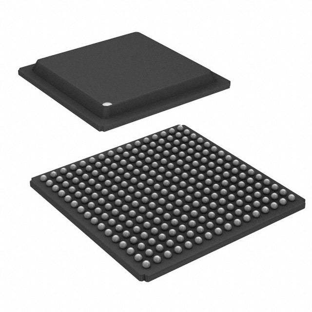
| 描述 | IC REG BCK SYNC ADJ 0.8A 12DSBGA |
| 产品分类 | |
| 品牌 | Texas Instruments |
| 数据手册 | |
| 产品图片 |
|
| 产品型号 | TPS62354YZGR |
| PWM类型 | 电压模式 |
| rohs | 无铅 / 符合限制有害物质指令(RoHS)规范要求 |
| 产品系列 | - |
| 产品目录页面 | |
| 供应商器件封装 | 12-DSBGA(1.53x1.98) |
| 其它名称 | 296-21645-6 |
| 包装 | Digi-Reel® |
| 同步整流器 | 是 |
| 安装类型 | 表面贴装 |
| 封装/外壳 | 12-UFBGA,DSBGA |
| 工作温度 | -40°C ~ 85°C |
| 标准包装 | 1 |
| 电压-输入 | 2.7 V ~ 5.5 V |
| 电压-输出 | 0.75 V ~ 1.54 V |
| 电流-输出 | 800mA |
| 类型 | 降压(降压) |
| 输出数 | 1 |
| 输出类型 | 可调式 |
| 频率-开关 | 3MHz |


- 商务部:美国ITC正式对集成电路等产品启动337调查
- 曝三星4nm工艺存在良率问题 高通将骁龙8 Gen1或转产台积电
- 太阳诱电将投资9.5亿元在常州建新厂生产MLCC 预计2023年完工
- 英特尔发布欧洲新工厂建设计划 深化IDM 2.0 战略
- 台积电先进制程称霸业界 有大客户加持明年业绩稳了
- 达到5530亿美元!SIA预计今年全球半导体销售额将创下新高
- 英特尔拟将自动驾驶子公司Mobileye上市 估值或超500亿美元
- 三星加码芯片和SET,合并消费电子和移动部门,撤换高东真等 CEO
- 三星电子宣布重大人事变动 还合并消费电子和移动部门
- 海关总署:前11个月进口集成电路产品价值2.52万亿元 增长14.8%


PDF Datasheet 数据手册内容提取
TPS62350, TPS62351 QFN-10 CSP-12 TPS62352, TPS62353 TPS62354, TPS62355, TPS62356 www.ti.com.............................................................................................................................................................. SLVS540E–MAY2006–REVISEDAPRIL2008 800-mA / 1000-mA, 3-MHz SYNCHRONOUS STEP-DOWN CONVERTER 2 WITH I C™ COMPATIBLE INTERFACE IN CHIP SCALE PACKAGING FEATURES 1 • 88%Efficiencyat3-MHzOperation DESCRIPTION 234 • 800-mAOutputCurrentatV =2.7V The TPS6235x device is a high-frequency I • 3-MHzFixedFrequencyOperation synchronous step-down dc-dc converter optimized for battery-powered portable applications. Intended for • BestinClassLoadandLineTransient low-power applications, the TPS6235x supports up to • Complete1-mmComponentProfileSolution 800-mA load current and allows the use of small, low • ±2%PWMDCVoltageAccuracy costinductorsandcapacitors. • 35-nsMinimumOn-Time The device is ideal for mobile phones and similar • EfficiencyOptimizedPower-SaveMode portable applications powered by a single-cell Li-Ion battery. With an output voltage range adjustable via (LightPFM) I2C interface down to 0.6 V, the device supports • TransientOptimizedPower-SaveMode low-voltage DSPs and processors core power (FastPFM) supplies in smart-phones, PDAs, and handheld • 28-m ATypicalQuiescentCurrent computers. • I2CCompatibleInterfaceupto3.4Mbps The TPS6235x operates at 3-MHz fixed switching • Pin-SelectableOutputVoltage frequency and enters the efficiency optimized power-save mode operation at light load currents to • SynchronizableOntheFlytoExternal maintain high efficiency over the entire load current ClockSignal range. In the shutdown mode, the current • Availableina10-PinQFN(3x3mm)and consumptionisreducedtolessthan2m A. 12-PinNanoFree™(CSP)Packaging The serial interface is compatible with Fast/Standard and High-Speed mode I2C specification allowing APPLICATIONS transfers at up to 3.4 Mbps. This communication • SmartReflex™CompliantPowerSupply interface is used for dynamic voltage scaling with • SplitSupplyDSPsandm PSolutions voltage steps down to 12.5 mV, for reprogramming the mode of operation (Light PFM, Fast PFM or OMAP™,XSCALE™ ForcedPWM)ordisable/enablingtheoutputvoltage. • CellPhones,Smart-Phones • PDAs,PocketPCs • DigitalCameras • MicroDC-DCConverterModules TYPICALAPPLICATION EFFICIENCYvs LOAD CURRENT TPS62350YZG 100 90 VI C1 PAVVIINN SFWB L1 VO −% 7800 2.7 V .. 5.5 V PPGGNNDD 1mH C102mF ncy 60 A AGND A cie 50 VO= FlIo2VCoOrB=u sRoof EVSSNSDCEALL Effi 12340000 VVLPIO=F= M3 1./6P.3 WV5 MV Mode up to 3.4 Mbips 0 SYNC 0.1 1 10 100 1000 IO−Output Current−mA 1 Pleasebeawarethatanimportantnoticeconcerningavailability,standardwarranty,anduseincriticalapplicationsof TexasInstrumentssemiconductorproductsanddisclaimerstheretoappearsattheendofthisdatasheet. NanoFree,SmartReflex,OMAP,PowerPADaretrademarksofTexasInstruments. 2 XSCALEisatrademarkofIntelCorporation. 3 I2CisatrademarkofPhilipsCorporation. 4 PRODUCTIONDATAinformationiscurrentasofpublicationdate. Copyright©2006–2008,TexasInstrumentsIncorporated Products conform to specifications per the terms of the Texas Instruments standard warranty. Production processing does not necessarilyincludetestingofallparameters.
TPS62350, TPS62351 TPS62352, TPS62353 TPS62354, TPS62355, TPS62356 SLVS540E–MAY2006–REVISEDAPRIL2008.............................................................................................................................................................. www.ti.com Thesedeviceshavelimitedbuilt-inESDprotection.Theleadsshouldbeshortedtogetherorthedeviceplacedinconductivefoam duringstorageorhandlingtopreventelectrostaticdamagetotheMOSgates. ORDERINGINFORMATION DEFAULT DEFAULT I2C NUPMABRETR(1) RVOOAUNLTTGPAEUGT(E2) VSVEOLO0LUTTAPGUEVTS(2E)L1 ENVB_AIDLTCU(2DE)C SYNC LSAB1BAITDSD(R2)EAS0S PACKAGE ORDERING(3) PMAACRKKAINGGE TPS62350(4) 0.75Vto1.5375V 1.05V 1.35V 1 YES 0 0 CSP-12 TPS62350YZG TPS62350 NO 1 0 QFN-10 TPS62351DRC BNT TPS62351 0.9Vto1.6875V 1.10V 1.50V 0 YES 1 0 CSP-12 TPS62351YZG TPS62351 TPS62352(4) 0.75Vto1.4375V 1.05V 1.20V 1 YES 1 0 CSP-12 TPS62352YZG TPS62352 TPS62353 0.75Vto1.5375V 1.00V 1.20V 1 YES 0 0 CSP-12 TPS62353YZG TPS62353 TPS62354(4) 0.75Vto1.5375V 1.05V 1.30V 1 YES 1 0 CSP-12 TPS62354YZG TPS62354 TPS62355(4) 0.75Vto1.5375V 0.90V 1.15V 1 NO 1 1 QFN-10 TPS62355DRC CCP TPS62356 1.5Vto1.975V 1.80V 1.80V 1 YES 0 0 CSP-12 TPS62356YZG TPS62356 (1) Alldevicesarespecifiedforoperationinthecommercialtemperaturerange,–40(cid:176) Cto85(cid:176) C. (2) Forcustomizedoutputvoltagerange,defaultoutputvoltageandI2Caddress,contactthefactory. (3) TheYZGpackageisavailableintapeandreel.AddRsuffix(TPS6235xYZGR,TPS6235xDRCR)toorderquantitiesof3000parts.Add Tsuffix(TPS6235xYZGT,TPS6235xDRCT)toorderquantitiesof250parts.Forthemostcurrentpackageandorderinginformation,see thePackageOptionAddendumattheendofthisdocument,orseetheTIwebsiteatwww.ti.com. (4) ThefollowingregistersbitsaresetbyinternalhardwarelogicandnotuserprogrammablethroughI2C: a.VSEL0[7:6]=11 b.VSEL1[7:6]=11 c.CONTROL1[4:2]=100 d.CONTROL2[7:6]=10,CONTROL2[4:3]=00 ABSOLUTE MAXIMUM RATINGS overoperatingfree-airtemperaturerange(unlessotherwisenoted)(1) UNITS VoltageatAVIN,PVIN(2) -0.3Vto7V VoltageatSW (2) -0.3Vto7V V I VoltageatEN,VSEL,SCL,SDA,SYNC (2) -0.3Vto7V VoltageatFB(2) -0.3Vto4.2V Powerdissipation Internallylimited T Maximumoperatingjunctiontemperature 150(cid:176) C J T Storagetemperaturerange –65(cid:176) Cto150(cid:176) C stg Humanbodymodel 2kV ESDrating(3) Chargedevicemodel 1kV Machinemodel 200V (1) Stressesbeyondthoselistedunderabsolutemaximumratingsmaycausepermanentdamagetothedevice.Thesearestressratings onlyandfunctionaloperationofthedeviceattheseoranyotherconditionsbeyondthoseindicatedunderrecommendedoperating conditionsisnotimplied.Exposuretoabsolute-maximum-ratedconditionsforextendedperiodsmayaffectdevicereliability. (2) Allvoltagevaluesarewithrespecttonetworkgroundterminal. (3) Thehumanbodymodelisa100-pFcapacitordischargedthrougha1.5-kΩresistorintoeachpin.Themachinemodelisa200-pF capacitordischargeddirectlyintoeachpin. 2 SubmitDocumentationFeedback Copyright©2006–2008,TexasInstrumentsIncorporated ProductFolderLink(s):TPS62350,TPS62351TPS62352,TPS62353TPS62354,TPS62355,TPS62356
TPS62350, TPS62351 TPS62352, TPS62353 TPS62354, TPS62355, TPS62356 www.ti.com.............................................................................................................................................................. SLVS540E–MAY2006–REVISEDAPRIL2008 RECOMMENDED OPERATING CONDITIONS overoperatingfree-airtemperaturerange(unlessotherwisenoted) MIN NOM MAX UNIT V Inputvoltagerange 2.7 5.5 V I T Operatingtemperaturerange(1) -40 85 (cid:176) C A T Operatingvirtualjunctiontemperaturerange -40 125 (cid:176) C J (1) Inapplicationswherehighpowerdissipationand/orpoorpackagethermalresistanceispresent,themaximumambienttemperaturemay havetobederated.Maximumambienttemperature(T )isdependentonthemaximumoperatingjunctiontemperature(T ),the A(max) J(max) maximumpowerdissipationofthedeviceintheapplication(P ),andthejunction-to-ambientthermalresistanceofthepart/package D(max) intheapplication(q ),asgivenbythefollowingequation:T =T –(q XP ). JA A(max) J(max) JA D(max) DISSIPATION RATINGS(1) PACKAGE Rq JA(2) PFOOWRETRR≤A2T5IN(cid:176) CG DAEBROATVIENGT F=A2C5T(cid:176)OCR A A DRC 49(cid:176) C/W 2050mW 21mW/(cid:176) C YZG 89(cid:176) C/W 1100mW 12mW/(cid:176) C (1) MaximumpowerdissipationisafunctionofT(max),q andT .Themaximumallowablepowerdissipationatanyallowableambient J JA A temperatureisP =[T(max)–T ]/q . D J A JA (2) Thisthermaldataismeasuredwithhigh-Kboard(4layersboardaccordingtoJESD51-7JEDECstandard). ELECTRICAL CHARACTERISTICS overoperatingfree-airtemperaturerange,typicalvaluesareatT =25(cid:176) C.Unlessotherwisenoted,specificationsapplywith A V =3.6V,EN=V,VSEL=V,SYNC=GND,VSEL0[6]bit=1. I I I PARAMETER TESTCONDITIONS MIN TYP MAX UNIT SUPPLYCURRENT TPS62350/1/2/3/4/5 IO=0mA,FastPFMmodeenabled 110 150 m A TPS62356 Devicenotswitching 117 160 Operatingquiescent IQ current TPS62350/1/2/3/4/5 IO=0mA,LightPFMmodeenabled 28 45 m A TPS62356 Devicenotswitching 35 52 TPS62350/1/2/3/4/5/6 IO=0mA,3-MHzPWMmodeoperation 4.8 mA EN=GND,EN_DCDCbit=X 0.1 2 m A I(SD) Shutdowncurrent EN=VI,EN_DCDCbit=0 6.5 m A V(UVLO) Undervoltagelockoutthreshold 2.20 2.3 V ENABLE,VSEL,SDA,SCL,SYNC VIH High-levelinputvoltage 1.2 V VIL Low-levelinputvoltage 0.4 V Ilkg Inputleakagecurrent InputtiedtoGNDorVI 0.01 1 m A POWERSWITCH VI=V(GS)=3.6V,YZGpackage 250 500 P-channelMOSFETon TPS62350/1/2/3/4/5 VI=V(GS)=3.6V,DRCpackage 275 500 rDS(on) resistance VI=V(GS)=2.7V,DRCpackage 350 750 mΩ TPS62356 VI=V(GS)=3.2V,YZGpackage 320 500 Ilkg P-channelleakagecurrent V(DS)=6V 1 m A VI=V(GS)=3.6V,YZGpackage 150 350 N-channelMOSFETon rDS(on) resistance TPS62350/1/2/3/4/5/6 VI=V(GS)=3.6V,DRCpackage 165 350 mΩ VI=V(GS)=2.7V,YZG/DRCpackage 210 500 Ilkg N-channelleakagecurrent V(DS)=6V 1 m A R(DIS) Dischargeresistorforpower-downsequence 15 50 Ω TPS62350/1/2/3/4/5 1150 1350 1600 mA P-MOScurrentlimit 2.7V≤VI≤5.5V TPS62356 1300 1550 1800 mA Copyright©2006–2008,TexasInstrumentsIncorporated SubmitDocumentationFeedback 3 ProductFolderLink(s):TPS62350,TPS62351TPS62352,TPS62353TPS62354,TPS62355,TPS62356
TPS62350, TPS62351 TPS62352, TPS62353 TPS62354, TPS62355, TPS62356 SLVS540E–MAY2006–REVISEDAPRIL2008.............................................................................................................................................................. www.ti.com ELECTRICAL CHARACTERISTICS (continued) overoperatingfree-airtemperaturerange,typicalvaluesareatT =25(cid:176) C.Unlessotherwisenoted,specificationsapplywith A V =3.6V,EN=V,VSEL=V,SYNC=GND,VSEL0[6]bit=1. I I I PARAMETER TESTCONDITIONS MIN TYP MAX UNIT N-MOScurrentlimit TPS62350/1/2/3/4/5 900 1100 1300 mA (sourcing) TPS62356 2.7V≤VI≤5.5V 1200 1400 1700 mA N-MOScurrentlimit TPS62350/1/2/3/4/5 -500 -700 -900 mA (sinking) TPS62356 2.7V≤VI≤5.5V -500 -700 -900 mA Inputcurrentlimitunder TPS62350/1/2/3/4/5 675 mA short-circuitconditions TPS62356 VO=0V 775 mA Thermalshutdown 150 (cid:176)C Thermalshutdownhysteresis 20 (cid:176)C OSCILLATOR fSW Oscillatorfrequency CONTROL2[4:3]=00 2.65 3 3.35 MHz f(SYNC) Synchronizationrange 2.65 3.35 MHz Dutycycleofexternalclocksignal 20% 80% OUTPUT TPS62350 0.75 1.5375 V TPS62351 0.90 1.6875 V TPS62352 0.75 1.4375 V VO Outputvoltagerange TPS62353 0.75 1.5375 V TPS62354 0.75 1.5375 V TPS62355 0.75 1.5375 V TPS62356 1.50 1.975 V ton(MIN) Minimumon-time(P-channelMOSFET) 35 ns ResistanceintoFBsensepin 700 1000 kΩ VI=3.6V,VO=1.35V,IO(DC)=0mA –1.5% 1.5% PWMoperation 2.7V≤VI≤5.5V,0mA≤IO(DC)≤800mA VO=0.75V,1.05V,1.35V,1.5375V –2% 2% PWMoperation Outputvoltage VO DCaccuracy TPS62350 2V.O7=V1≤.0V5I≤V,5L.5=V1,ImOH(D,CL)i=gh0tmPFAM –1% 4.5% 2V.O7=V1≤.3V5I≤V,5L.5=V1,0m Hm,AFa≤sItOP(DFCM)≤/P8W00MmA –2% 3% 2V.O7=V1≤.0V5I≤V,5L.5=V1,0m Hm,ALi≤ghIOt(oDrCF)≤as8t0P0FmMA/PWM –2% 4.5% VI=3.6V,VO=1.50V,IO(DC)=0mA –1.5% 1.5% PWMoperation 2.7V≤VI≤5.5V,0mA≤IO(DC)≤800mA VO=0.90V,1.10V,1.50V,1.6875V –2% 2% PWMoperation Outputvoltage VO DCaccuracy TPS62351 2V.O7=V1≤.1V0I≤V,5L.5=V1,ImOH(D,CL)i=gh0tmPFAM –1% 4.5% 2V.O7=V1≤.1V0I≤V,5L.5=V1,0m Hm,ALi≤ghIOt(oDrCF)≤as8t0P0FmMA/PWM –2% 4.5% 2V.O7=V1≤.5V0I≤V,5L.5=V1,0m Hm,ALi≤ghIOt(oDrCF)≤as8t0P0FmMA/PWM –2% 4.0% VI=3.6V,VO=1.20V,IO(DC)=0mA –1.5% 1.5% PWMoperation 2.7V≤VI≤5.5V,0mA≤IO(DC)≤800mA VO=0.75V,1.05V,1.20V,1.4375V –2% 2% PWMoperation Outputvoltage VO DCaccuracy TPS62352 2V.O7=V1≤.0V5I≤V,5L.5=V1,ImOH(D,CL)i=gh0tmPFAM –1% 4.5% 2V.O7=V1≤.2V0I≤V,5L.5=V1,0m Hm,AFa≤sItOP(DFCM)≤/P8W00MmA –2% 3% 2V.O7=V1≤.0V5I≤V,5L.5=V1,0m Hm,ALi≤ghIOt(oDrCF)≤as8t0P0FmMA/PWM –2% 4.5% 4 SubmitDocumentationFeedback Copyright©2006–2008,TexasInstrumentsIncorporated ProductFolderLink(s):TPS62350,TPS62351TPS62352,TPS62353TPS62354,TPS62355,TPS62356
TPS62350, TPS62351 TPS62352, TPS62353 TPS62354, TPS62355, TPS62356 www.ti.com.............................................................................................................................................................. SLVS540E–MAY2006–REVISEDAPRIL2008 ELECTRICAL CHARACTERISTICS (continued) overoperatingfree-airtemperaturerange,typicalvaluesareatT =25(cid:176) C.Unlessotherwisenoted,specificationsapplywith A V =3.6V,EN=V,VSEL=V,SYNC=GND,VSEL0[6]bit=1. I I I PARAMETER TESTCONDITIONS MIN TYP MAX UNIT VI=3.6V,VO=1.20V,IO(DC)=0mA –1.5% 1.5% PWMoperation 2.7V≤VI≤5.5V,0mA≤IO(DC)≤800mA VO=0.75V,1.00V,1.20V,1.5375V –2% 2% PWMoperation Outputvoltage VO DCaccuracy TPS62353 2V.O7=V1≤.0V0I≤V,5L.5=V1,ImOH(D,CL)i=gh0tmPFAM, –1% 4.5% 2V.O7=V1≤.2V0I≤V,5L.5=V1,0m Hm,AFa≤sItOP(DFCM)≤/P8W00MmA –2% 3% 2V.O7=V1≤.0V0I≤V,5L.5=V1,0m Hm,ALi≤ghIOt(oDrCF)≤as8t0P0FmMA/PWM –2% 4.5% VI=3.6V,VO=1.30V,IO(DC)=0mA, –1.5% 1.5% PWMoperation 2.7V≤VI≤5.5V,0mA≤IO(DC)≤800mA VO=0.75V,1.05V,1.30V,1.5375V –2% 2% PWMoperation Outputvoltage VO DCaccuracy TPS62354 2V.O7=V1≤.0V5I≤V,5L.5=V1,ImOH(D,CL)i=gh0tmPFAM, –1% 4.5% 2V.O7=V1≤.3V0I≤V,5L.5=V1,0m Hm,AFa≤sItOP(DFCM)≤/P8W00MmA –2% 3% 2V.O7=V1≤.0V5I≤V,5L.5=V1,0m Hm,ALi≤ghIOt(oDrCF)≤as8t0P0FmMA/PWM –2% 4.5% VI=3.6V,VO=1.15V,IO(DC)=0mA, –1.5% 1.5% PWMoperation 2.7V≤VI≤5.5V,0mA≤IO(DC)≤800mA VO=0.75V,0.9V,1.15V,1.5375V –2% 2% PWMoperation Outputvoltage VO DCaccuracy TPS62355 2V.O7=V0≤.9VVI≤,L5.=51V,m IHO,(DLCi)g=ht0PmFMA –1% 4.5% 2V.O7=V1≤.1V5I≤V,5L.5=V1,0m Hm,AFa≤sItOP(DFCM)≤/P8W00MmA –2% 3% 2V.O7=V0≤.9VVI≤,L5.=51V,m 0H,mLAig≤htIOo(rDFC)a≤st8P0F0Mm/PAWM –2% 4.5% 2.7V≤VI≤3.2V,0mA≤IO(DC)≤800mA 3.2V≤VI≤5.5V,0mA≤IO(DC)≤1000mA(1) –2% 2% VO=1.80V PWMoperation Outputvoltage 2V.O7=V1≤.8V0I≤V,5L.5=V1,ImOH(D,CL)i=gh0tmPFAM –1% 4.5% VO DCaccuracy TPS62356 2.7V≤VI≤3.2V,0mA≤IO(DC)≤800mA 3.2V≤VI≤5.5V,0mA≤IO(DC)≤1000mA(1) –2% 3% VO=1.80V,L=1m H,FastPFM/PWM 2.7V≤VI≤3.2V,0mA≤IO(DC)≤800mA 3.2V≤VI≤5.5V,0mA≤IO(DC)≤1000mA(1) –2% 4.5% VO=1.80V,L=1m H,LightorFastPFM/PWM DCoutputvoltageloadregulation IO(DC)=0mAto800mA,PWMoperation –0.0003 %/mA ΔVO DCoutputvoltagelineregulation VI=VO+0.5V(min2.7V)to5.5V, 0 %/V IO(DC)=300mA VLiOgh=t0P.F9MV,oIpOe(DraC)tio=n0mA,L=1m H, 33 mVPP VLiOgh=t1P.F0M5Vo,pIeOr(aDtCio)n=1mA,L=1m H, 30 mVPP Power-savemoderipplevoltage VLO==11m.H10,LVig,hIOt(PDCF)M=o1pmerAa,tion,VSEL0[6]bit=0 12 mVPP VLO==11m.H35,FVa,sItO(PDFC)M=o1pemrAat,ion 0.025VO VPP (1) Inapplicationswherehighpowerdissipationand/orpoorpackagethermalresistanceispresent,themaximumambienttemperaturemay havetobederated.Maximumambienttemperature(T )isdependentonthemaximumoperatingjunctiontemperature(T ),the A(max) J(max) maximumpowerdissipationofthedeviceintheapplication(P ),andthejunction-to-ambientthermalresistanceofthepart/package D(max) intheapplication(q ),asgivenbythefollowingequation:T =T –(q XP ). JA A(max) J(max) JA D(max) Copyright©2006–2008,TexasInstrumentsIncorporated SubmitDocumentationFeedback 5 ProductFolderLink(s):TPS62350,TPS62351TPS62352,TPS62353TPS62354,TPS62355,TPS62356
TPS62350, TPS62351 TPS62352, TPS62353 TPS62354, TPS62355, TPS62356 SLVS540E–MAY2006–REVISEDAPRIL2008.............................................................................................................................................................. www.ti.com ELECTRICAL CHARACTERISTICS (continued) overoperatingfree-airtemperaturerange,typicalvaluesareatT =25(cid:176) C.Unlessotherwisenoted,specificationsapplywith A V =3.6V,EN=V,VSEL=V,SYNC=GND,VSEL0[6]bit=1. I I I PARAMETER TESTCONDITIONS MIN TYP MAX UNIT Ilkg LeakagecurrentintoSWpin VI>VO,0V≤V(SW)≤VI,EN=GND 0.01 1 m A ReverseleakagecurrentintoSWpin VI=open,V(SW)=6V,EN=GND 0.01 1 DAC TPS62350 TPS62351 TPS62352 Resolution TPS62353 6 Bits TPS62354 TPS62355 TPS62356 Differentialnonlinearity Specifiedmonotonicbydesign ±0.8 LSB TIMING SetupTimeBetweenRisingENandStartofI2C 250 m s Stream VO Otimuetputvoltagesettling TPS62350 FIOr(oDmC)=mi5n0t0ommAa,xPoWutMpuotpveorltaatgioen, 3 m s TimefromactiveENtoVO 180 VO=1.35V,RL=5Ω,PWMoperation TPS62350 TimefromactiveENtoVO 170 VO=1.05V,IO(DC)=0mA,LightPFMoperation Start-uptime TPS62351 TimefromactiveEN_DCDCbittoVO 45 m s VO=1.5V,RL=5Ω,PWMoperation TimefromactiveENtoVO 175 VO=1.2V,RL=5Ω,PWMoperation TPS62352 TimefromactiveENtoVO 170 VO=1.05V,IO(DC)=0mA,LightPFMoperation I2C INTERFACE TIMING CHARACTERISTICS(1) PARAMETER TESTCONDITIONS MIN MAX UNIT Standardmode 100 kHz Fastmode 400 kHz High-speedmode(writeoperation),C –100pFmax 3.4 MHz B f SCLClockFrequency (SCL) High-speedmode(readoperation),C –100pFmax 3.4 MHz B High-speedmode(writeoperation),C –400pFmax 1.7 MHz B High-speedmode(readoperation),C –400pFmax 1.7 MHz B BusFreeTimeBetweenaSTOPand Standardmode 4.7 m s t BUF STARTCondition Fastmode 1.3 m s Standardmode 4 m s HoldTime(Repeated)START t ,t Fastmode 600 ns HD STA Condition High-speedmode 160 ns Standardmode 4.7 m s Fastmode 1.3 m s t LOWPeriodoftheSCLClock LOW High-speedmode,C –100pFmax 160 ns B High-speedmode,C –400pFmax 320 ns B Standardmode 4 m s Fastmode 600 ns t HIGHPeriodoftheSCLClock HIGH High-speedmode,C –100pFmax 60 ns B High-speedmode,C –400pFmax 120 ns B (1) Specifiedbydesign.Nottestedinproduction. 6 SubmitDocumentationFeedback Copyright©2006–2008,TexasInstrumentsIncorporated ProductFolderLink(s):TPS62350,TPS62351TPS62352,TPS62353TPS62354,TPS62355,TPS62356
TPS62350, TPS62351 TPS62352, TPS62353 TPS62354, TPS62355, TPS62356 www.ti.com.............................................................................................................................................................. SLVS540E–MAY2006–REVISEDAPRIL2008 I2C INTERFACE TIMING CHARACTERISTICS (continued) PARAMETER TESTCONDITIONS MIN MAX UNIT Standardmode 4.7 m s SetupTimeforaRepeatedSTART t ,t Fastmode 600 ns SU STA Condition High-speedmode 160 ns Standardmode 250 ns t ,t DataSetupTime Fastmode 100 ns SU DAT High-speedmode 10 ns Standardmode 0 3.45 m s Fastmode 0 0.9 m s t ,t DataHoldTime HD DAT High-speedmode,C –100pFmax 0 70 ns B High-speedmode,C –400pFmax 0 150 ns B Standardmode 20+0.1C 1000 ns B Fastmode 20+0.1C 300 ns B t RiseTimeofSCLSignal RCL High-speedmode,C –100pFmax 10 40 ns B High-speedmode,C –400pFmax 20 80 ns B Standardmode 20+0.1C 1000 ns B RiseTimeofSCLSignalAftera Fastmode 20+0.1C 300 ns B t RepeatedSTARTConditionandAfter RCL1 anAcknowledgeBIT High-speedmode,CB–100pFmax 10 80 ns High-speedmode,C –400pFmax 20 160 ns B Standardmode 20+0.1C 300 ns B Fastmode 20+0.1C 300 ns B t FallTimeofSCLSignal FCL High-speedmode,C –100pFmax 10 40 ns B High-speedmode,C –400pFmax 20 80 ns B Standardmode 20+0.1C 1000 ns B Fastmode 20+0.1C 300 ns B t RiseTimeofSDASignal RDA High-speedmode,C –100pFmax 10 80 ns B High-speedmode,C –400pFmax 20 160 ns B Standardmode 20+0.1C 300 ns B Fastmode 20+0.1C 300 ns B t FallTimeofSDASignal FDA High-speedmode,C –100pFmax 10 80 ns B High-speedmode,C –400pFmax 20 160 ns B Standardmode 4 m s t ,t SetupTimeforSTOPCondition Fastmode 600 ns SU STO High-speedmode 160 ns C CapacitiveLoadforSDAandSCL 400 pF B Copyright©2006–2008,TexasInstrumentsIncorporated SubmitDocumentationFeedback 7 ProductFolderLink(s):TPS62350,TPS62351TPS62352,TPS62353TPS62354,TPS62355,TPS62356
TPS62350, TPS62351 TPS62352, TPS62353 TPS62354, TPS62355, TPS62356 SLVS540E–MAY2006–REVISEDAPRIL2008.............................................................................................................................................................. www.ti.com I2C TIMING DIAGRAMS SDA tf tLOW tr tsu;DAT tf thd;STA tr tBUF SCL thd;STA tsu;STA tsu;STO S thd;DAT HIGH Sr P S Figure1.SerialInterfaceTimingDiagramforF/S-Mode Sr Sr P tfDA trDA SDAH thd;DAT tsu;STO tsu;STA thd;STA tsu;DAT SCLH tfCL trCL1 trCL trCL1 See Note A tHIGH tLOW tLOW tHIGH See Note A = MCS Current Source Pull-Up = R(P) Resistor Pull-Up Note A: First rising edge of the SCLH signal after Sr and after each acknowledge bit. Figure2.SerialInterfaceTimingDiagramforHS-Mode 8 SubmitDocumentationFeedback Copyright©2006–2008,TexasInstrumentsIncorporated ProductFolderLink(s):TPS62350,TPS62351TPS62352,TPS62353TPS62354,TPS62355,TPS62356
TPS62350, TPS62351 TPS62352, TPS62353 TPS62354, TPS62355, TPS62356 www.ti.com.............................................................................................................................................................. SLVS540E–MAY2006–REVISEDAPRIL2008 PIN ASSIGNMENTS TPS6235x TPS6235x TPS6235x QFN−10 CSP−12 CSP−12 (TOP VIEW) (TOP VIEW) (BOTTOM VIEW) A1 A2 A3 A3 A2 A1 B1 B2 B3 B3 B2 B1 C1 C2 C3 C3 C2 C1 D1 D2 D3 D3 D2 D1 TERMINALFUNCTIONS TERMINAL NO. NO. I/O DESCRIPTION NAME QFN CSP PVIN 1 A3 Supplyvoltageforoutputpowerstage. AVIN 2 B3 Thisistheinputvoltagepinofthedevice.Connectdirectlytotheinputbypasscapacitor. Thisistheenablepinofthedevice.Connectthispintogroundforcesthedeviceintoshutdown mode.PullingthispintoV enablesthedevice.Ontherisingedgeoftheenablepin,allthe EN 7 C2 I I registersareresetwiththeirdefaultvalues.Thispinmustnotbeleftfloatingandmustbe terminated. VSELsignalisprimarilyusedtoscaletheoutputvoltageandtosettheTPS6235xoperation VSEL 5 D2 I betweenactivemode(VSEL=HIGH)andsleepmode(VSEL=LOW).Themodeofoperationcan alsobeadaptedbyI2Csettings.Thispinmustnotbeleftfloatingandmustbeterminated. SDA 3 C3 I/O Serialinterfaceaddress/dataline SCL 4 D3 I Serialinterfaceclockline FB 6 D1 I Outputfeedbacksenseinput.ConnectFBtotheconverteroutput. AGND 8 C1 Analogground Inputforsynchronizationtoexternalclocksignal.Synchronizestheconverterswitchingfrequency SYNC N/A B2 I toanexternalclocksignal.Thispinmustnotbeleftfloatingandmustbeterminated.Connecting SYNCtostatichighorlowstatehasnoeffectontheconverteroperation. PGND 9 A1B1 Powerground.ConnecttoAGNDunderneathIC. SW 10 A2 I/O ThisistheswitchpinoftheconverterandconnectedtothedrainoftheinternalpowerMOSFETs. PowerPAD™ N/A InternallyconnectedtoPGND. Copyright©2006–2008,TexasInstrumentsIncorporated SubmitDocumentationFeedback 9 ProductFolderLink(s):TPS62350,TPS62351TPS62352,TPS62353TPS62354,TPS62355,TPS62356
TPS62350, TPS62351 TPS62352, TPS62353 TPS62354, TPS62355, TPS62356 SLVS540E–MAY2006–REVISEDAPRIL2008.............................................................................................................................................................. www.ti.com FUNCTIONAL BLOCK DIAGRAM SYNC EN PVIN N-MOS Current Limit Compator _ SSDCAL I2C I/F RCeLgooinsgttiercorsl 6D-ABCit VDAC 3 MHz Soft-Start PowMeord Seave + REF Oscillator + PLL Comp Low Sawtooth Switching + VSEL Generator EN Discharge Logic _ REF P-MOS Current Limit ò Compator 2R FB R C - + - Gate Driver - + - SW Anti 2C Shoot-Through R(DIS) + +- + + + P EN Discharge P FB Undervoltage AVIN BiLaos cSkuopuptly A Comp Low + _ VONOM Bandgap VREF= 0.4 V AGND Thermal PGND Shutdown PARAMETER MEASUREMENT INFORMATION U1 PVIN FB VI C1 AVIN SW L1 VO 10mF PGND C2 2.7 V .. 6 V 10mF PGND A AGND A V EN I VSEL SDA I2C Bus SCL SYNC List of Components: U1 = TPS6235x L1 = FDK MIPSA2520 Series C1, C2 = TDK C1608X5R0G106MT Note: The internal registers are set to their default values. 10 SubmitDocumentationFeedback Copyright©2006–2008,TexasInstrumentsIncorporated ProductFolderLink(s):TPS62350,TPS62351TPS62352,TPS62353TPS62354,TPS62355,TPS62356
TPS62350, TPS62351 TPS62352, TPS62353 TPS62354, TPS62355, TPS62356 www.ti.com.............................................................................................................................................................. SLVS540E–MAY2006–REVISEDAPRIL2008 TYPICAL CHARACTERISTICS Table of Graphs FIGURE vsOutputcurrent 3,4,5,6 h Efficiency vsInputvoltage 7 vsOutputcurrent 8,9,12 DCoutputvoltage vsInputvoltage 10,11 V O vsAmbienttemperature 13 Measuredoutputvoltage vsDACtargetoutputvoltage 14 I Quiescentcurrent vsInputvoltage 15 Q I Shutdowncurrent vsInputvoltage 16 SD f Oscillatorfrequency vsInputvoltage 17 (OSC) P-channelMOSFETr vsInputvoltage 18 DS(on) r DS(on) N-channelMOSFETr vsInputvoltage 19 DS(on) I Inductorpeakcurrent vsAmbienttemperature 20 P 21,22,23,24,25,26 Loadtransientresponse 27,28,29,30,31,32 Linetransientresponse 33 Combinedlineandloadtransient 34 response PWMoperation 35 Dutycyclejitter 36 Power-savemodeoperation 37,38 Dynamicvoltagemanagement 39,40 Outputvoltagerampcontrol 41 Start-up 42,43 EFFICIENCY EFFICIENCY vs vs OUTPUTCURRENT OUTPUTCURRENT 100 100 90 LPFM/PWM 90 LPFM/PWM 80 80 70 70 % % − 60 − 60 y y c c n 50 n 50 e e ci FPFM/PWM 3-MHz PWM ci FPFM/PWM Effi 40 Effi 40 30 30 V = 3.6 V V = 3.6 V I I 20 V = 1.35 V 20 V = 1.05 V O O L= 1mH L= 1mH 10 10 C = 10mF C = 10mF O O 0 0 0.1 1 10 100 1000 0.1 1 10 100 1000 I −Output Current−mA I −Output Current−mA O O Figure3. Figure4. Copyright©2006–2008,TexasInstrumentsIncorporated SubmitDocumentationFeedback 11 ProductFolderLink(s):TPS62350,TPS62351TPS62352,TPS62353TPS62354,TPS62355,TPS62356
TPS62350, TPS62351 TPS62352, TPS62353 TPS62354, TPS62355, TPS62356 SLVS540E–MAY2006–REVISEDAPRIL2008.............................................................................................................................................................. www.ti.com EFFICIENCY EFFICIENCY vs vs OUTPUTCURRENT OUTPUTCURRENT 100 100 LPFM/PWM VI= 3.6 V 90 90 V = 1.35 V O C = 10mF 80 80 O 3-MHz PWM Mode 70 70 % % L= 2.2mH − 60 − 60 y y c c en 50 3-MHz PWM en 50 L= 1mH ci ci Effi 40 FPFM/PWM Effi 40 30 30 V = 3.6 V I 20 V = 1.5 V 20 O L= 1mH 10 10 C = 10mF O 0 0 0.1 1 10 100 1000 1 10 100 1000 I −Output Current−mA I −Output Current−mA O O Figure5. Figure6. EFFICIENCY DCOUTPUTVOLTAGE vs vs INPUTVOLTAGE OUTPUTCURRENT 100 1.373 I = 500 mA O 90 80 1.363 FPFM/PWM Mode V 70 − e g −% 60 IO= 1 mA IO= 10 mA olta 1.353 y V nc 50 ut PWM Mode e p ci IO= 100 mA ut Effi 40 C O 1.343 I = 200 mA D 30 O − O V 20 1.333 V = 1.35 V L= 1mH VI = 3.6 V L= 1mH 10 FPOFM/PWM Mode CO= 10mF VO = 1.35 V CO= 10mF 0 1.323 2.72.9 3.13.3 3.5 3.73.9 4.1 4.3 4.5 4.74.95.1 5.35.5 0.1 1 10 100 1000 VI−Input Voltage−V IO−Output Current−mA Figure7. Figure8. 12 SubmitDocumentationFeedback Copyright©2006–2008,TexasInstrumentsIncorporated ProductFolderLink(s):TPS62350,TPS62351TPS62352,TPS62353TPS62354,TPS62355,TPS62356
TPS62350, TPS62351 TPS62352, TPS62353 TPS62354, TPS62355, TPS62356 www.ti.com.............................................................................................................................................................. SLVS540E–MAY2006–REVISEDAPRIL2008 DCOUTPUTVOLTAGE DCOUTPUTVOLTAGE vs vs OUTPUTCURRENT INPUTVOLTAGE 1.070 0.790 V = 0.75 V O 0.785 1.065 L= 1mH I = 100mA C = 10mF O LPFM/PWM Mode 0.780 O LPFM/PWM Mode V 1.060 V 0.775 − − e e ag 1.055 ag 0.770 ut Volt 1.050 PWM Mode ut Volt 0.765 IO= 100 mA utp utp 0.760 IO= 10 mA O O C 1.045 C 0.755 D D − − 0.750 O1.040 O V V 0.745 1.035 VI = 3.6 V L= 1mH IO= 400 mA VO = 1.05 V CO= 10mF 0.740 1.030 0.735 0.1 1 10 100 1000 2.72.9 3.13.3 3.5 3.73.9 4.1 4.3 4.5 4.74.95.1 5.35.5 IO−Output Current−mA VI−Input Voltage−V Figure9. Figure10. DCOUTPUTVOLTAGE DCOUTPUTVOLTAGE vs vs INPUTVOLTAGE OUTPUTCURRENT 1.525 0.930 VO = 1.5 V VO = 0.9 V LPFM/PWM Mode 1.520 L= 1mH 0.925 L= 1mH LPFM Ovsptimize Bit C = 10mF IO= 100mA CO = 10mF O 1.515 LPFM/PWM Mode 0.920 V V − − IO= 100mA, bit = 1 ge 1.510 ge 0.915 Volta 1.505 IO= 10 mA Volta 0.910 IO= 10 mA, bit = 1 ut ut p p ut 1.500 IO= 100 mA ut 0.905 O O C C D 1.495 D 0.900 − − VO1.490 IO= 400 mA VO0.895 IO= 100mA, bit = 0 IO= 10 mA, bit = 0 1.485 0.890 IO= 400 mA, bit = 0 1.480 0.885 2.72.9 3.13.3 3.5 3.73.9 4.1 4.3 4.5 4.74.95.1 5.35.5 2.72.9 3.13.3 3.5 3.73.9 4.1 4.3 4.5 4.74.95.1 5.35.5 V −Input Voltage−V V −Input Voltage−V I I Figure11. Figure12. Copyright©2006–2008,TexasInstrumentsIncorporated SubmitDocumentationFeedback 13 ProductFolderLink(s):TPS62350,TPS62351TPS62352,TPS62353TPS62354,TPS62355,TPS62356
TPS62350, TPS62351 TPS62352, TPS62353 TPS62354, TPS62355, TPS62356 SLVS540E–MAY2006–REVISEDAPRIL2008.............................................................................................................................................................. www.ti.com DCOUTPUTVOLTAGE MEASUREDOUTPUTVOLTAGE vs vs AMBIENTTEMPERATURE DACTARGETOUTPUTVOLTAGE 1.360 5 I = 100 mA O 4 L= 1mH 1.355 C = 10mF V O m 3 V 3-MHz PWM Mode V = 2.7 V − T = 85oC − I e A put Voltage 11..335405 utput Voltag 21 TA= 25oC ut O 0 C O VI = 3.6 V VI = 4.5 V red TA= -40oC D 1.340 u -1 s − a O e V M -2 − 1.335 O VI = 3.6 V V -3 IO= 100 mA L= 1mH 3 MHz PWM Mode CO= 10mF 1.330 -4 -40 -30 -20 -10 0 10 20 30 40 50 60 70 8085 0.75 0.85 0.95 1.05 1.15 1.25 1.35 1.45 1.55 T −Ambient Temperature−oC V −DAC Target Output Voltage−V A O Figure13. Figure14. QUIESCENTCURRENT SHUTDOWNCURRENT vs vs INPUTVOLTAGE INPUTVOLTAGE 50 10 V = 1.05 V O LPFM Mode 9 45 A T = 85oC TA= 25oC m 8 A A − nt−m 40 TA= 85oC rrent 7 re Cu 6 Cur TA= 25oC wn cent 35 utdo 5 TA= -30oC s h 4 e S ui 30 − −Q SD) 3 IQ TA= -40oC I( 2 25 EN = High 1 EN_DCDC bit = 0 20 0 2.72.9 3.13.3 3.5 3.73.9 4.1 4.3 4.5 4.74.95.1 5.35.5 2.72.9 3.13.3 3.5 3.73.9 4.1 4.3 4.5 4.74.95.1 5.35.5 V −Input Voltage−V V −Input Voltage−V I I Figure15. Figure16. 14 SubmitDocumentationFeedback Copyright©2006–2008,TexasInstrumentsIncorporated ProductFolderLink(s):TPS62350,TPS62351TPS62352,TPS62353TPS62354,TPS62355,TPS62356
TPS62350, TPS62351 TPS62352, TPS62353 TPS62354, TPS62355, TPS62356 www.ti.com.............................................................................................................................................................. SLVS540E–MAY2006–REVISEDAPRIL2008 OSCILLATORFREQUENCY r P-MOSFET DS(on) vs vs INPUTVOLTAGE INPUTVOLTAGE 3.15 450 T = -40oC A 400 Hz 3.1 TA= 85oC M T = 25oC − A W y m 350 c 3.05 n − reque SFET 300 TA= 25oC or F 3 T = 85oC MO at A P- 250 −Oscill 2.95 −DS(on) 200 TA= -40oC C) r S f(O 2.9 150 2.85 100 2.72.9 3.13.3 3.5 3.73.9 4.1 4.3 4.5 4.74.95.1 5.35.5 2.72.9 3.13.3 3.5 3.73.9 4.1 4.3 4.5 4.74.95.1 5.35.5 V −Input Voltage−V V −Input Voltage−V I I Figure17. Figure18. r N-MOSFET INDUCTORPEAKCURRENT DS(on) vs vs INPUTVOLTAGE AMBIENTTEMPERATURE 275 1.7 Closed Loop V = 4.5 V 250 1.6 I T = 85oC A A mW 225 −nt 1.5 VI= 3.6 V − re T 200 ur OSFE 175 TA= 25oC eak C 1.4 VI= 2.7 V M P N- or 1.3 − 150 ct on) du rDS( 125 −In 1.2 TA= -40oC IP 1.1 100 75 1 2.72.9 3.13.3 3.5 3.73.9 4.1 4.3 4.5 4.74.95.1 5.35.5 -40 -30 -20 -10 0 10 20 30 40 50 60 70 8085 VI−Input Voltage−V TA−Ambient Temperature−oC Figure19. Figure20. Copyright©2006–2008,TexasInstrumentsIncorporated SubmitDocumentationFeedback 15 ProductFolderLink(s):TPS62350,TPS62351TPS62352,TPS62353TPS62354,TPS62355,TPS62356
TPS62350, TPS62351 TPS62352, TPS62353 TPS62354, TPS62355, TPS62356 SLVS540E–MAY2006–REVISEDAPRIL2008.............................................................................................................................................................. www.ti.com LOADTRANSIENT:50mA/400mA/50mA LOADTRANSIENT:50mA/400mA PWMOPERATION PWMOPERATION v v di di A/ A/ IO0 m IO0 m VI= 3.6 V 20 20 VO= 1.35 V L= 1mH C = 10mF O 3-MHz PWM Mode et et s s Off Off V V 5- 5- VO1.3 VI= 3.6 V VO1.3 - V = 1.35 V - v O v di L= 1mH di mV/ CO= 10mF mV/ 0 3-MHz PWM Mode 0 1 1 t−Time = 50ms/div t−Time = 5ms/div Figure21. Figure22. LOADTRANSIENT:400mA/50mA LOADTRANSIENT:50mA/400mA/50mA PWMOPERATION FPFM/PWMOPERATION V = 3.6 V v I v A/di VO= 1.35 V A/di IOm 3-MHz PWM Mode IOm 0 0 0 0 2 2 et et s s Off Off V V 5- 5- 3 3 VO1. VO1. - - v v V/di L= 1mH V/di L= 1mH VI= 3.6 V 10 m CO= 10mF 20 m CO= 10mF VFPOF=M 1/P.3W5 MV Mode t−Time = 5ms/div t−Time = 50ms/div Figure23. Figure24. 16 SubmitDocumentationFeedback Copyright©2006–2008,TexasInstrumentsIncorporated ProductFolderLink(s):TPS62350,TPS62351TPS62352,TPS62353TPS62354,TPS62355,TPS62356
TPS62350, TPS62351 TPS62352, TPS62353 TPS62354, TPS62355, TPS62356 www.ti.com.............................................................................................................................................................. SLVS540E–MAY2006–REVISEDAPRIL2008 LOADTRANSIENT:50mA/400mA LOADTRANSIENT:400mA/50mA FPFM/PWMOPERATION FPFM/PWMOPERATION V = 3.6 V v v I di di V = 1.35 V A/ A/ O IOm IOm FPFM/PWM Mode 0 0 0 0 2 2 et et s s Off Off V V 5- 5- 3 3 VO1. VO1. - - v v mV/di L= 1mH VVI== 3 1.6.3 V5 V mV/di L= 1mH 20 CO= 10mF FPOFM/PWM Mode 20 CO= 10mF t−Time = 10ms/div t−Time = 10ms/div Figure25. Figure26. LOADTRANSIENT:400mA/750mA/400mA LOADTRANSIENT:400mA/750mA PWMOPERATION PWMOPERATION Offset Offset A A m m IO400 - IO400 - div div VI= 3.6 V mA/ mA/ VO= 1.35 V 200 200 3-MHz PWM Mode Offset Offset V V VO1.35-- VO1.35-- div VI= 3.6 V div L= 1mH 10 mV/ V3-OM=H z1 .P35W VM Mode LCO= =1 1m0HmF 10 mV/ CO= 10mF t−Time = 50ms/div t−Time = 5ms/div Figure27. Figure28. Copyright©2006–2008,TexasInstrumentsIncorporated SubmitDocumentationFeedback 17 ProductFolderLink(s):TPS62350,TPS62351TPS62352,TPS62353TPS62354,TPS62355,TPS62356
TPS62350, TPS62351 TPS62352, TPS62353 TPS62354, TPS62355, TPS62356 SLVS540E–MAY2006–REVISEDAPRIL2008.............................................................................................................................................................. www.ti.com LOADTRANSIENT:750mA/400mA LOADTRANSIENT:1mA/100mA/1mA PWMOPERATION LFPM/PWMOPERATION set VI= 3.6 V Off VI= 3.6 V VO= 1.05 V mA VO= 1.35 V v 0 3-MHz PWM Mode di O40 OA/ I - Im v 0 di 5 A/ m 0 0 2 et et s s Off Off V V 5- 5- 3 0 VO1. VO1. - - v v di L= 1mH di mV/ C = 10mF mV/ L= 1mH 10 O 10 CO= 10mF LPFM Mode t−Time = 5ms/div t−Time = 50ms/div Figure29. Figure30. LOADTRANSIENT:1mA/100mA LOADTRANSIENT:100mA/1mA LPFM/PWMOPERATION LPFM/PWMOPERATION VI= 3.6 V LPFM Mode VI= 3.6 V div VO= 1.05 V div VO= 1.05 V IOmA/ IOmA/ LPFM Mode 0 0 0 0 1 1 v v di di A/ A/ ILm ILm 0 0 0 0 2 2 et et s s Off Off V V 5- 5- 0 0 VO1.- VO1.- L= 1mH div L= 1mH div CO= 10mF mV/ CO= 10mF mV/ 0 0 1 1 t−Time = 2ms/div t−Time = 2ms/div Figure31. Figure32. 18 SubmitDocumentationFeedback Copyright©2006–2008,TexasInstrumentsIncorporated ProductFolderLink(s):TPS62350,TPS62351TPS62352,TPS62353TPS62354,TPS62355,TPS62356
TPS62350, TPS62351 TPS62352, TPS62353 TPS62354, TPS62355, TPS62356 www.ti.com.............................................................................................................................................................. SLVS540E–MAY2006–REVISEDAPRIL2008 COMBINEDLINE/LOADTRANSIENT LINETRANSIENT (3.6VTO4.2V,400mATO800mA) PWMOPERATION PWMOPERATION 6-V Offset IV3O-OM=H= 5 z10 .P 3mW5A MV Mode LCO= =1 1m0HmF 3-V Offset 500 mIOA/div VI3.- VIv- mV/div mV/di 0 0 0 0 5 5 et V Offs Offset VOdiv1.35-- VO1.35-V - V/ v VO= 1.35 V 10 m mV/di 3 MHz PWM Mode t−Time = 100ms/div 50 t−Time = 10ms/div Figure33. Figure34. PWMOPERATION DUTYCYCLEJITTER div VIOI== 32.060 V m, VAO= 1.35 V 3-MHz PWM Mode VLI== 13.m6 HV,,VCOO== 11.035m FV IO= 200 mA A/ ILm 0 0 2 SW2 V/div V/div) 1 W ( et S s Off V 5- 3 VO1. - div L= 1mH V/ C = 10mF 3-MHz PWM Mode m O 0 2 t−Time = 200 ns/div t−Time = 50 ns/div Figure35. Figure36. Copyright©2006–2008,TexasInstrumentsIncorporated SubmitDocumentationFeedback 19 ProductFolderLink(s):TPS62350,TPS62351TPS62352,TPS62353TPS62354,TPS62355,TPS62356
TPS62350, TPS62351 TPS62352, TPS62353 TPS62354, TPS62355, TPS62356 SLVS540E–MAY2006–REVISEDAPRIL2008.............................................................................................................................................................. www.ti.com POWERSAVEMODEOPERATION POWERSAVEMODEOPERATION v v di di A/ A/ ILm ILm 0 0 0 0 2 2 et et s s Off Off V V 5- 5- 3 0 VO1. VO1. - - div VI= 3.6 V L= 1mH div VI= 3.6 V L= 1mH mV/ VO= 1.35 V CO= 10mF mV/ VO= 1.05 V CO= 10mF 20 IO= 40 mA FPFM Mode 20 IO= 1 mA LPFM Mode t−Time = 2.5ms/div t−Time = 40ms/div Figure37. Figure38. DYNAMICVOLTAGEMANAGEMENT DYNAMICVOLTAGEMANAGEMENT VI= 3.6 V ELdiv ELdiv VO= 1.05 V (LPFM)/ 1.35 V (PWM) SV/ SV/ V2 VO= 1.35 V V2 VO= 1.35 V Offset Offset V V VO1.05-- PWM VO= 1.05 V VO1.05-- PWM VO= 1.05 V V/div FPFM V/div LPFM m m 100 100 v v di di ILmA/ ILmA/ 500 VVIO== 3 1.6.0 V5 V (FPFM)/ 1.35 V (PWM) RL= 5W 200 RL= 270W t−Time = 20ms/div t−Time = 50ms/div Figure39. Figure40. 20 SubmitDocumentationFeedback Copyright©2006–2008,TexasInstrumentsIncorporated ProductFolderLink(s):TPS62350,TPS62351TPS62352,TPS62353TPS62354,TPS62355,TPS62356
TPS62350, TPS62351 TPS62352, TPS62353 TPS62354, TPS62355, TPS62356 www.ti.com.............................................................................................................................................................. SLVS540E–MAY2006–REVISEDAPRIL2008 OUTPUTVOLTAGE RAMPCONTROL STARTUP ELdiv Ndiv SV/ EV/ V2 VI= 3.6 V 2 VO= 0.75 V/ 1.5 V (PWM) VI= 3.6 V IO= 0 mA v VO= 1.05 V (LPFM) VO= 1.5 V OV/di IO= 0 mA Vm 0 0 5 et s Off V 5- Slew Rate = 4.5 mV/ms 7 VOmV/div0.- IL0 mA/div 0 VO= 0.75 V 20 0 2 t−Time = 50ms/div t−Time = 50ms/div Figure41. Figure42. STARTUP v Ndi EV/ V = 3.6 V 2 I V = 1.35 V (PWM) O R = 5W L v di OV/ Vm 0 0 5 v di A/ ILm 0 0 5 t−Time = 50ms/div Figure43. Copyright©2006–2008,TexasInstrumentsIncorporated SubmitDocumentationFeedback 21 ProductFolderLink(s):TPS62350,TPS62351TPS62352,TPS62353TPS62354,TPS62355,TPS62356
TPS62350, TPS62351 TPS62352, TPS62353 TPS62354, TPS62355, TPS62356 SLVS540E–MAY2006–REVISEDAPRIL2008.............................................................................................................................................................. www.ti.com DETAILED DESCRIPTION Operation The TPS6235x is a synchronous step-down converter typically operating with a 3-MHz fixed frequency pulse width modulation (PWM) at moderate to heavy load currents. At light load currents, the converter operates in power-save mode with pulse frequency modulation (PFM). The device integrates two power-save modes optimized either for ultra-high efficiency at light load (light PFM) or for transient response when turning in PWM operation (fast PFM). Both power-save modes automatically transition to PWM operation when the load current increases. The TPS6235x integrates an I2C compatible interface allowing transfers up to 3.4 Mbps. This communication interface can be used for dynamic voltage scaling with voltage steps down to 12.5 mV (or to 25 mV steps for TPS62356), for reprogramming the mode of operation (light PFM, fast PFM or forced PWM) or disable/enabling theoutputvoltageforinstance.Formoredetails,seetheI2Cinterfaceandregisterdescriptionsection. During PWM operation, the converter uses a unique fast response, voltage mode, control scheme with input voltage feed-forward. This achieves best-in-class load and line response and allows the use of tiny inductors and small ceramic input and output capacitors. At the beginning of each switching cycle, the P-channel MOSFET switch is turned on and the inductor current ramps up until the comparator trips and the control logic turns off the switch. The operating frequency is set to 3 MHz and can be synchronized on-the-fly to an external oscillator or to amasterdc/dcconverter(refertoapplicationexamples). The device integrates two current limits, one in the P-channel MOSFET and another one in the N-channel MOSFET. When the current in the P-channel MOSFET reaches its current limit, the P-channel MOSFET is turned off and the N-channel MOSFET is turned on. When the current in the N-channel MOSFET is above the N-MOS current limit threshold, the N-channel MOSFET remains on until the current drops below its current limit. The current limit in the N-channel MOSFET is important for small duty-cycle operation when the current in the inductor does not decrease because of the P-channel MOSFET current limit delay, or because of start-up conditionswheretheoutputvoltageislow. Power-Save Mode : Fast PFM With decreasing load current, the device automatically switches into pulse skipping operation in which the power stage operates intermittently based on load demand. By running cycles periodically, the switching losses are minimized,andthedevicerunswithaminimumquiescentcurrentandmaintainshighefficiency. In fast PFM mode, the converter only operates when the output voltage trips below a set threshold voltage (V O nominal). It ramps up the output voltage with several pulses and goes into power-save mode when the inductor current reaches zero. As a consequence in power-save mode the average output voltage is slightly higher than its nominal value in PWM mode. The fast PFM mode is optimized for fast response when transitioning between pulseskippingandPWMoperation. PFM Mode at Light Load PFM Ripple Comp Low Threshold = VONOM PWM Mode at Heavy Load Figure44.OperationinPFMModeandTransfertoPWMMode 22 SubmitDocumentationFeedback Copyright©2006–2008,TexasInstrumentsIncorporated ProductFolderLink(s):TPS62350,TPS62351TPS62352,TPS62353TPS62354,TPS62355,TPS62356
TPS62350, TPS62351 TPS62352, TPS62353 TPS62354, TPS62355, TPS62356 www.ti.com.............................................................................................................................................................. SLVS540E–MAY2006–REVISEDAPRIL2008 Power-Save Mode : Light PFM With decreasing load current, the device can also automatically switch into light PFM pulse skipping operation in which the power stage operates intermittently based on load demand. The advantage of the light PFM is much lowerI (28m A)anddrasticallyhigherefficiencycomparedwithfastPFMinlowoutputloads. Q In light PFM mode, the converter only operates when the output voltage trips below a set threshold voltage (V nominal). It ramps up the output voltage with one or several pulses and goes back into power-save mode. As O a consequence in power-save mode the average output voltage is slightly higher than its nominal value in PWM mode. In order to get a proper transition between light PFM and PWM operation, the output voltage ripple (in light PFM mode) has been made proportional to the input voltage. It is possible to reduce the output voltage ripple by setting the LIGHTPFM OPTIMIZE (VSEL0[6] or VSEL1[6]) bit low. However, this is only practical in applications operating with a 1-m H (typical) inductor, with a load current less than V / 25 Ω and which do not require the I auto-modetransitionfunction. When operating with a 2.2-m H (typical) inductor, the LIGHTPFM OPTIMIZE (VSEL0[6] or VSEL1[6]) bit should always be set to low. In this case, the auto-mode transition is fully functional without any restriction on the load current. Mode Selection and Frequency Synchronization The TPS6235x can be synchronized to an external clock signal by the SYNC pin. Pulling the SYNC pin to a staticstatehighorlowstatehasnoeffectontheconverter'soperation. Depending on the settings of CONTROL1 register the device can be operated in either the fixed frequency PWM mode or in the automatic PWM and power-save mode. In this mode, the converter operates in fixed frequency PWM mode at moderate to heavy loads and in the PFM mode during light loads, which maintains high efficiency overawideloadcurrentrange.Formoredetails,seetheCONTROL1registerdescription. The fixed frequency PWM mode has the tightest regulation and the best line/load transient performance. Furthermore, this mode of operation allows simple filtering of the switching frequency for noise-sensitive applications. In fixed frequency PWM mode, the efficiency is lower compared to the power-save mode during light loads. It is possible to switch from power-save mode (light or fast PWM) to forced PWM mode during operation either via the VSEL signal or by re-programming the CONTROL1 register. This allows adjustments to the converters operation to match the specific system requirements leading to more efficient and flexible power management. When the synchronization is enabled (CONTROL2[5]=1), the mode is set to fixed-frequency operation and the P-channel MOSFET turn on is synchronized to the falling edge of the external clock. This creates the ability for multiple converters to be connected together in a master-slave configuration for frequency matching of the converters(seetheapplicationsectionformoredetails). When CONTROL1[1:0]=00 and VSEL signal is low, the converter operates according to MODE0 bit and the synchronizationisdisabledregardlessofEN_SYNCandHW_nSWbits. Soft Start The TPS6235x has an internal soft-start circuit that limits the inrush current during start-up. This prevents possible input voltage drops when a battery or a high-impedance power source is connected to the input of the converter. In the TPS62350/1/2/3/4/5 devices, the soft start is implemented as a digital circuit increasing the switch current in steps of typically 350 mA, 675 mA, 1000 mA, and the typical switch current limit of 1350 mA. The current limit transitions to the next step every 256 clocks (» 88m s). To be able to switch from 675 mA to 1000 mA current limit step, the output voltage needs to be higher than 0.5 x V (otherwise the parts keeps operating at 675 mA O(NOM) currentlimit). In the TPS62356 device, the soft start is implemented as a digital circuit increasing the switch current in steps of typically 400 mA, 775 mA, 1150 mA, and the typical switch current limit of 1550 mA. The current limit transitions to the next step every 256 clocks (» 88m s). To switch from 775 mA to 1150 mA current limit step, the output voltageneedstobehigherthan0.5xV (otherwisethepartskeepsoperatingat775mAcurrentlimit). O(NOM) Copyright©2006–2008,TexasInstrumentsIncorporated SubmitDocumentationFeedback 23 ProductFolderLink(s):TPS62350,TPS62351TPS62352,TPS62353TPS62354,TPS62355,TPS62356
TPS62350, TPS62351 TPS62352, TPS62353 TPS62354, TPS62355, TPS62356 SLVS540E–MAY2006–REVISEDAPRIL2008.............................................................................................................................................................. www.ti.com This mechanism is used to limit the output current under short-circuit conditions. Therefore, the start-up time dependsontheoutputcapacitorandloadcurrent. Enable The device starts operation when EN pin is set high and starts up with the soft start. This signal is gated by the EN_DCDCbitdefinedinregisterVSEL0andVSEL1.Onrisingedge of the EN pin, all the registers are reset with their default values. Enabling the converter's operation via the EN_DCDC bit does not affect internal register settings. This allows the output voltage to be programmed to other values than the default voltage before starting uptheconverter.Formoredetails,seetheVSEL0/1registerdescription. Pulling the EN pin, VSEL0[6] bit or VSEL1[6] bit low forces the device into shutdown, with a shutdown current as defined in the electrical characteristics table. In this mode, the P and N-channel MOSFETs are turned off, the internalresistorfeedbackdividerisdisconnected, and the entire internal-control circuitry is switched off. When an output voltage is present during shutdown mode, which is caused by an external voltage source or super capacitor, the reverse leakage is specified under electrical characteristics. For proper operation, the EN pin must beterminatedandmustnotbeleftfloating. In addition, depending on the setting of CONTROL2[6] bit, the device can actively discharge the output capacitor when it turns off. The integrated discharge resistor has a typical resistance of 15 Ω. The required time to dischargetheoutputcapacitoratV dependsonloadcurrentandtheoutputcapacitancevalue. O Voltage and Mode Selection The TPS6235x features a pin-selectable output voltage. VSEL is primarily used to scale the output voltage between active (VSEL=HIGH) and sleep mode (VSEL=LOW). For maximum flexibility, it is possible to reprogram the operating mode of the converter (e.g. fixed frequency PWM, fast PFM or light PFM) associated with VSEL signalviatheI2Cinterface VSELoutputvoltageandmodeselectionisdefinedasfollowing: VSEL=LOW:DC/DCoutputvoltagedeterminedbyVSEL0registervalue.DC/DCmodeofoperationis determinedbyMODE0bitinCONTROL1register VSEL=HIGH:DC/DCoutputvoltagedeterminedbyVSEL1registervalue.DC/DCmodeofoperationis determinedbyMODE1bitinCONTROL1register. Undervoltage Lockout The undervoltage lockout circuit prevents the device from misoperation at low input voltages. It prevents the converterfromturningontheswitchorrectifierMOSFETunderundefinedconditions. Short-Circuit Protection As soon as the output voltage falls below 50% of the nominal output voltage, the converter current limit is reduced by 50% of the nominal value. Because the short-circuit protection is enabled during start-up, the device does not deliver more than half of its nominal current limit until the output voltage exceeds 50% of the nominal output voltage. This needs to be considered when a load acting as a current sink is connected to the output of theconverter. Thermal Shutdown As soon as the junction temperature, T , exceeds 150(cid:176) C typical, the device goes into thermal shutdown. In this J mode, the P- and N-channel MOSFETs are turned off. The device continues its operation when the junction temperaturefallsbelow130(cid:176) Ctypicalagain. 24 SubmitDocumentationFeedback Copyright©2006–2008,TexasInstrumentsIncorporated ProductFolderLink(s):TPS62350,TPS62351TPS62352,TPS62353TPS62354,TPS62355,TPS62356
TPS62350, TPS62351 TPS62352, TPS62353 TPS62354, TPS62355, TPS62356 www.ti.com.............................................................................................................................................................. SLVS540E–MAY2006–REVISEDAPRIL2008 THEORY OF OPERATION Serial Interface Description I2C is a 2-wire serial interface developed by Philips Semiconductor (see I2C-Bus Specification, Version 2.1, January 2000). The bus consists of a data line (SDA) and a clock line (SCL) with pull-up structures. When the bus is idle, both SDA and SCL lines are pulled high. All the I2C compatible devices connect to the I2C bus through open drain I/O pins, SDA and SCL. A master device, usually a microcontroller or a digital signal processor, controls the bus. The master is responsible for generating the SCL signal and device addresses. The master also generates specific conditions that indicate the START and STOP of data transfer. A slave device receivesand/ortransmitsdataonthebusundercontrolofthemasterdevice. The TPS6235x device works as a slave and supports the following data transfer modes, as defined in the I2C-Bus Specification: standard mode (100 kbps), fast mode (400 kbps), and high-speed mode (up to 3.4 Mbps in write mode). The interface adds flexibility to the power supply solution, enabling most functions to be programmed to new values depending on the instantaneous application requirements. Register contents remain intactaslongassupplyvoltageremainsabove2.2V(typical). The data transfer protocol for standard and fast modes is exactly the same, therefore, they are referred to as F/S-modeinthisdocument.Theprotocolforhigh-speedmodeis different from the F/S-mode, and it is referred to as HS-mode. The TPS6235x device supports 7-bit addressing; 10-bit addressing and general call address are notsupported. The TPS6235x device has a 7-bit address with the 2 LSB bits factory programmable allowing up to four dc/dc converterstobeconnectedtothesamebus.The5MSBsare10010. F/S-ModeProtocol The master initiates data transfer by generating a start condition. The start condition is when a high-to-low transitionoccursontheSDAlinewhileSCLishigh,seeFigure45.AllI2C-compatibledevices should recognize a startcondition. The master then generates the SCL pulses, and transmits the 7-bit address and the read/write direction bit R/W on the SDA line. During all transmissions, the master ensures that data is valid. A valid data condition requires the SDA line to be stable during the entire high period of the clock pulse, see Figure 46. All devices recognize the address sent by the master and compare it to their internal fixed addresses. Only the slave device with a matching address generates an acknowledge, see Figure 47, by pulling the SDA line low during the entire high period of the ninth SCL cycle. Upon detecting this acknowledge, the master knows that the communication link withaslavehasbeenestablished. The master generates further SCL cycles to either transmit data to the slave (R/W bit 1) or receive data from the slave (R/W bit 0). In either case, the receiver needs to acknowledge the data sent by the transmitter. An acknowledge signal can either be generated by the master or by the slave, depending on which one is the receiver. 9-bit valid data sequences consisting of 8-bit data and 1-bit acknowledge can continue as long as necessary. To signal the end of the data transfer, the master generates a stop condition by pulling the SDA line from low to high while the SCL line is high, see Figure 45. This releases the bus and stops the communication link with the addressed slave. All I2C compatible devices must recognize the stop condition. Upon the receipt of a stop condition, all devices know that the bus is released, and they wait for a start condition followed by a matching address AttemptingtoreaddatafromregisteraddressesnotlistedinthissectionresultsinFFhbeingreadout. H/S-ModeProtocol Whenthebusisidle,bothSDAandSCLlinesarepulledhighbythepull-updevices. The master generates a start condition followed by a valid serial byte containing HS master code 00001XXX. This transmission is made in F/S-mode at no more than 400 Kbps. No device is allowed to acknowledge the HS mastercode,butalldevicesmustrecognizeitandswitchtheirinternalsettingtosupport3.4-Mbpsoperation. Copyright©2006–2008,TexasInstrumentsIncorporated SubmitDocumentationFeedback 25 ProductFolderLink(s):TPS62350,TPS62351TPS62352,TPS62353TPS62354,TPS62355,TPS62356
TPS62350, TPS62351 TPS62352, TPS62353 TPS62354, TPS62355, TPS62356 SLVS540E–MAY2006–REVISEDAPRIL2008.............................................................................................................................................................. www.ti.com Themasterthengeneratesarepeatedstartcondition(arepeated start condition has the same timing as the start condition). After this repeated start condition, the protocol is the same as F/S-mode, except that transmission speeds up to 3.4 Mbps are allowed. A stop condition ends the HS-mode and switches all the internal settings of the slave devices to support the F/S-mode. Instead of using a stop condition, repeated start conditions are used tosecurethebusinHS-mode. AttemptingtoreaddatafromregisteraddressesnotlistedinthissectionresultsinFFhbeingreadout. DATA CLK S P Start Stop Condition Condition Figure45.STARTandSTOPConditions DATA CLK Data Line Stable; Change of Data Allowed Data Valid Figure46.BitTransferontheSerialInterface Data Output by Transmitter Not Acknowledge Data Output by Receiver Acknowledge SCL From 1 2 8 9 Master S Clock Pulse for START Acknowledgement Condition Figure47.AcknowledgeontheI2CBus 26 SubmitDocumentationFeedback Copyright©2006–2008,TexasInstrumentsIncorporated ProductFolderLink(s):TPS62350,TPS62351TPS62352,TPS62353TPS62354,TPS62355,TPS62356
TPS62350, TPS62351 TPS62352, TPS62353 TPS62354, TPS62355, TPS62356 www.ti.com.............................................................................................................................................................. SLVS540E–MAY2006–REVISEDAPRIL2008 Recognize START or Recognize STOP or REPEATED START REPEATED START Condition Condition Generate ACKNOWLEDGE Signal P SDA MSB Acknowledgement Sr Signal From Slave Address R/W SCL 1 2 7 8 9 1 2 3 − 8 9 S Sr ACK ACK or or Sr P Clock Line Held Low While Interrupts are Serviced START or STOP or Repeated START Repeated START Condition Condition Figure48.BusProtocol TPS6235xI2CUpdateSequence The TPS6235x requires a start condition, a valid I2C address, a register address byte, and a data byte for a single update. After the receipt of each byte, TPS6235x device acknowledges by pulling the SDA line low during thehighperiodofasingleclockpulse.Avalid I2C address selects the TPS6235x. TPS6235x performs an update onthefallingedgeoftheLSBbyte. When the TPS6235x is in hardware shutdown (EN pin tied to ground) the device can not be updated via the I2C interface.Conversely,theI2Cinterfaceisfullyfunctionalduringsoftwareshutdown(EN_DCDCbit=0). 1 7 1 1 8 1 8 1 1 S SlaveAddress R/W A RegisterAddress A Data A P “0”Write FromMastertoTPS6235x A=Acknowledge S=STARTcondition P=STOPcondition FromTPS6235xtoMaster Figure49."Write"DataTransferFormatinF/S-Mode Copyright©2006–2008,TexasInstrumentsIncorporated SubmitDocumentationFeedback 27 ProductFolderLink(s):TPS62350,TPS62351TPS62352,TPS62353TPS62354,TPS62355,TPS62356
TPS62350, TPS62351 TPS62352, TPS62353 TPS62354, TPS62355, TPS62356 SLVS540E–MAY2006–REVISEDAPRIL2008.............................................................................................................................................................. www.ti.com 1 7 1 1 8 1 1 7 1 1 8 1 1 S SlaveAddress R/W A RegisterAddress A Sr SlaveAddress R/W A Data A P “0”Write “1”Read A =Acknowledge FromMastertoTPS6235x S =STARTcondition Sr=REPEATEDSTARTcondition FromTPS6235xtoMaster P =STOPcondition Figure50."Read"DataTransferFormatinF/S-Mode F/S Mode HS Mode F/S Mode S HS-MASTER CODE A Sr SLAVEADDRESS R/W A REGISTERADDRESS A DATA A/A P ”0”(write) Data Transferred HS Mode Continues (n x Bytes +Acknowledge) Sr SlaveAddress Figure51.DataTransferFormatinH/S-Mode SlaveAddressByte MSB LSB X 1 0 0 1 0 A1 A0 The slave address byte is the first byte received following the START condition from the master device. The first five bits (MSBs) of the address are factory preset to 10010. The next two bits (A1, A0) of the address are device option dependent. For example, TPS62350 is factory preset to 00 and TPS62351 is preset to 10. Up to 4 TPS62350 type of devices can be connected to the same I2C-Bus. See the ordering information table for more details. RegisterAddressByte MSB LSB 0 0 0 0 0 0 D1 D0 Following the successful acknowledgment of the slave address, the bus master sends a byte to the TPS6235x, whichcontainstheaddressoftheregistertobe accessed. The TPS6235x contains four 8-bit registers accessible viaabidirectionalI2C-businterface.Allinternalregistershavereadandwriteaccess. Table1.RegisterDescription Name Description VSEL0(read/write) 00 VSEL1(read/write) 01 CONTROL1(read/write) 10 CONTROL2(read/write) 11 28 SubmitDocumentationFeedback Copyright©2006–2008,TexasInstrumentsIncorporated ProductFolderLink(s):TPS62350,TPS62351TPS62352,TPS62353TPS62354,TPS62355,TPS62356
TPS62350, TPS62351 TPS62352, TPS62353 TPS62354, TPS62355, TPS62356 www.ti.com.............................................................................................................................................................. SLVS540E–MAY2006–REVISEDAPRIL2008 Voltage Scaling Management In order to reduce the power consumption of the processor core, the TPS6235x can scale its output voltage. Therearetwodifferentstrategies:1)bysoftwareor2)byhardware.Itcanbeselected by the HW_nSW bit (more informationofthecontrolandvaluebitmentionedbelowisshownintheRegisterDescriptionsection). SynchronizedScalingHardwareStrategy(HW_nSW=1) The application processor programs via I2C the output voltages associated with the two states of VSEL signal: floor (VSEL0) and roof (VSEL1) values. The application processor also writes the DEFSLEW value in the CONTROL2registertocontroltheoutputvoltageramprate. These two registers can be continuously updated via I2C to provide the appropriate output voltage according to the VSEL input. The voltage changes with the selected ramp rate immediately after writing to the VSEL0 or VSEL1register. InPFMmode,whentheoutputvoltageisprogrammedtoa lower value by toggling VSEL signal from high to low, PWROK is defined as low, while the output capacitor is discharged by the load until the converter starts pulsing tomaintainthevoltagewithinregulation. In multiple-step mode, PWROK is defined as low while the output voltage is ramping up or down. Under all other operatingconditions,PWROKisdefinedtobelowwhentheoutputvoltageisbelow-1.5%ofthetargetvalue. V NOM (ROOF) V NOM (FLOOR) Output Voltage Change Initiated Comp Low Threshold: V NOM (ROOF) PWROK Figure52.PWROKOperation(TransitiontoaLowerVoltage) Table2showstheoutputvoltagestatesdependingonVSEL0,VSEL1registers,andVSELsignal. Table2.SynchronizedScalingHardwareStrategyOverview(HW_nSW=1) VSELPIN VSEL0REGISTER VSEL1REGISTER OUTPUTVOLTAGE Low Noaction Noaction Floor Low Writenewvalue Noaction Changetonewvalue Low Noaction Write Nochangestaysatfloorvoltage High Noaction Noaction Roof High Writenewvalue Noaction Nochangestaysatroofvoltage High Noaction Writenewvalue Changetonewvalue DirectScalingSoftwareStrategy(HW_nSW=0) The digital processor writes the output voltage needed directly to the register VSEL1 via I2C interface. The application processor also writes the DEFSLEW value in the CONTROL2 register to control the output voltage ramprate. The voltage changes with the selected ramp rate after setting the GO bit in CONTROL2 register. This bit is reset when the output voltage has reached its target value. In this mode, the output voltage change is independent of VSELsignalandVSEL0registerisnotused. In PFM mode, when the output voltage is programmed to a lower value, PWROK is defined as low while the output capacitor is discharged by the load until the converter starts pulsing to maintain the voltage within regulation. Copyright©2006–2008,TexasInstrumentsIncorporated SubmitDocumentationFeedback 29 ProductFolderLink(s):TPS62350,TPS62351TPS62352,TPS62353TPS62354,TPS62355,TPS62356
TPS62350, TPS62351 TPS62352, TPS62353 TPS62354, TPS62355, TPS62356 SLVS540E–MAY2006–REVISEDAPRIL2008.............................................................................................................................................................. www.ti.com In multiple-step mode, PWROK is defined as low while the output voltage is ramping up or down. Under all other operatingconditions,PWROKisdefinedtobelowwhentheoutputvoltageisbelow-1.5%ofthetargetvalue. VoltageRampControl TheTPS6235xoffersavoltagerampratecontrolthatcanoperateintwodifferentmodes: • Multiple-StepMode • Single-StepMode ThemodeisselectedviaDEFSLEWcontrolbitsintheCONTROL2register. Single-StepVoltageScalingMode(default),DEFSLEW[2:0]=[111] In single-step mode, the TPS6235x ramps the output voltage with maximum slew-rate when transitioning betweenthefloorandtheroofvoltages(switchtoahighervoltage). When switching between the roof and the floor voltages (transition to a lower voltage), the ramp rate control is dependent on the mode selection (see CONTROL1 register) associated with the target register (Forced PWM, Fast,orLightPFM). Table 3 shows the ramp rate control when transitioning to a lower voltage with DEFSLEW set to immediate transition. Table3.RampRateControlvs.TargetMode ModeAssociatedwith HW_nSW OutputVoltageRampRate TargetVoltage ForcedPWM X Immediate FastPFM X Timetorampdowndependsonoutputcapacitanceandloadcurrent LightPFM X Timetorampdowndependsonoutputcapacitanceandloadcurrent For instance, when the output is programmed to transition to a lower voltage with Light or Fast PFM operation enabled, the TPS6235x ramps down the output voltage without controlling the ramp rate or having intermediate micro-steps. The required time to ramp down the voltage depends on the capacitance present at the output of the TPS6235x and on the load current. From an overall system perspective, this is the most efficient way to performdynamicvoltagescaling. Multiple-StepVoltageScalingMode,DEFSLEW[2:0]=[000]to[110] In multiple-step mode the TPS6235x controls the output voltage ramp rate regardless of the HW_nSW bit and of the mode of operation (e.g. Forced PWM, Fast PFM, or Light PFM). The voltage ramp control is done by adjustingthetimebetweenthevoltagemicro-steps. 30 SubmitDocumentationFeedback Copyright©2006–2008,TexasInstrumentsIncorporated ProductFolderLink(s):TPS62350,TPS62351TPS62352,TPS62353TPS62354,TPS62355,TPS62356
TPS62350, TPS62351 TPS62352, TPS62353 TPS62354, TPS62355, TPS62356 www.ti.com.............................................................................................................................................................. SLVS540E–MAY2006–REVISEDAPRIL2008 REGISTER DESCRIPTION VSEL0REGISTER(READ/WRITE) MSB LSB Memory location: 00 7 6 5 4 3 2 1 0 Reset state:X1XX XXXX–See the Ordering InformationTable VOLTAGE STEPMULTIPLIER, VSM0 6-bit unsigned binary linear coding. Code effective from 0 to 63 decimal LIGHTPFM OPTIMIZE 0 : LightPFM optimized for 2.2-mH inductor 1 : LightPFM optimized for 1-mH inductor (default) This bit is internally mapped by VSEL1[6]. Writing a value in VSEL0[6] automatically updates VSEL1[6]. EN_DCDC This bit gates the external EN pin signal 0 : Device in shutdown regardless of EN signal 1 : Device enabled when EN pin tied high (default) This bit is internally mapped by VSEL1[7]. Writing a value in VSEL0[7] automatically updates VSEL1[7]. A. TPS62350,51,52,53,54,55:OutputVoltage=MinimumOutputVoltage+(VoltageStepMultiplier0x12.5mV) B. TPS62356:OutputVoltage=MinimumOutputVoltage+(VoltageStepMultiplier0x25mV) VSEL1REGISTER(READ/WRITE) MSB LSB Memory location: 01 7 6 5 4 3 2 1 0 Reset state: X1XX XXXX–See the Ordering InformationTable VOLTAGE STEPMULTIPLIER, VSM1 6-bit unsigned binary linear coding. Code effective from 0 to 63 decimal LIGHTPFM OPTIMIZE 0 : LightPFM optimized for 2.2-mH inductor 1 : LightPFM optimized for 1-mH inductor (default) This bit is internally mapped by VSEL0[6]. Writing a value in VSEL1[6] automatically updates VSEL0[6]. EN_DCDC This bit gates the external EN pin signal 0 : Device in shutdown regardless of EN signal 1 : Device enabled when EN pin tied high (default) This bit is internally mapped by VSEL0[7]. Writing a value in VSEL1[7] automatically updates VSEL0[7]. A. TPS62350,51,52,53,54,55:OutputVoltage=MinimumOutputVoltage+(VoltageStepMultiplier1x12.5mV) B. TPS62356:OutputVoltage=MinimumOutputVoltage+(VoltageStepMultiplier1x25mV) Copyright©2006–2008,TexasInstrumentsIncorporated SubmitDocumentationFeedback 31 ProductFolderLink(s):TPS62350,TPS62351TPS62352,TPS62353TPS62354,TPS62355,TPS62356
TPS62350, TPS62351 TPS62352, TPS62353 TPS62354, TPS62355, TPS62356 SLVS540E–MAY2006–REVISEDAPRIL2008.............................................................................................................................................................. www.ti.com CONTROL1REGISTER(READ/WRITE) MSB LSB Memory location: 02 7 6 5 4 3 2 1 0 Reset state: 0001 0000 MODE0 This bit defines the mode of operation for VSELlow 0 : Light PFM with auto. transition to PWM (default) 1 : Fast PFM with auto. transition to PWM MODE1 This bit defines the mode of operation for VSELhigh 0 : Forced PWM (default) 1 : Fast PFM with auto. transition to PWM MODE_CTRL 00 : Operation follows MODE0, MODE1 (default) 01 : Light PFM with auto. transition to PWM (VSELindependent) 10 : Forced PWM (VSELindependent) 11 : Fast PFM with auto. transition to PWM (VSELindependent) HW_nSW 0 : Output voltage controlled by software to the value defined in VSEL1. 1 : Output voltage controlled by VSELpin (default) EN_SYNC 0 : Disable synchronization to external clock signal (default) 1 : Enable synchronization to external clock signal RESERVED (00) 32 SubmitDocumentationFeedback Copyright©2006–2008,TexasInstrumentsIncorporated ProductFolderLink(s):TPS62350,TPS62351TPS62352,TPS62353TPS62354,TPS62355,TPS62356
TPS62350, TPS62351 TPS62352, TPS62353 TPS62354, TPS62355, TPS62356 www.ti.com.............................................................................................................................................................. SLVS540E–MAY2006–REVISEDAPRIL2008 CONTROL2REGISTER(READ/WRITE) MSB LSB Memory location: 03 7 6 5 4 3 2 1 0 Reset state: 0000 0111 DEFSLEW DEFSLEW defines the output voltage ramp rate 000 : 0.15 mV/ms 001 : 0.3 mV/ms 010 : 0.6 mV/ms 011 : 1.2 mV/ms 100 : 2.4 mV/ms 101 : 4.8 mV/ms 110 : 9.6 mV/ms 111 : Immediate (default) PLL_MULT PLL_MULTdefines the synchronization clock multiplier ratio 00 : x1 - f = 3 MHz ± 12% (default) (SYNC) 01 : x2 - f = 1.5 MHz ± 12% (SYNC) 10 : x3 - f = 1 MHz ± 12% (SYNC) 11 : x4 - f = 750 kHz ± 12% (SYNC) PWROK (READ ONLY) 0 : Indicates that the output voltage is below its target regulation voltage.This bit is zero if the converter is disabled. 1 : Indicates that the output voltage is within its nominal range OUTPUT_DISCHARGE 0 :The dc/dc output capacitor is not actively discharged when the converter is disabled (default). 1 :The dc/dc output capacitor is actively discharged when the converter is disabled. GO This bit is only valid when HW_nSW = 0 0 : No change in the output voltage(default). 1 :The output voltage is changed with the ramp rate defined in DEFSLEW. Copyright©2006–2008,TexasInstrumentsIncorporated SubmitDocumentationFeedback 33 ProductFolderLink(s):TPS62350,TPS62351TPS62352,TPS62353TPS62354,TPS62355,TPS62356
TPS62350, TPS62351 TPS62352, TPS62353 TPS62354, TPS62355, TPS62356 SLVS540E–MAY2006–REVISEDAPRIL2008.............................................................................................................................................................. www.ti.com APPLICATION INFORMATION Output Filter Design (Inductor and Output Capacitor) The TPS6235x step-down converter has an internal loop compensation. Therefore, the external L-C filter must beselectedtoworkwiththeinternalcompensation. Thedevicehasbeendesignedtooperatewithinductancevaluesbetweenaminimumof0.7m Handmaximum of 6.2 m H. The internal compensation is optimized to operate with an output filter of L = 1 m H and C = 10 m F. Such O anoutputfilterhasitscornerfrequencyat: ƒc(cid:2) 1 (cid:2) 1 (cid:2)50.3kHz 2(cid:2)(cid:3)L(cid:1)CO 2(cid:2)(cid:3)1(cid:1)H(cid:1)10(cid:1)F (1) Selecting a larger output capacitor value (e.g., 22 m F) is less critical because the corner frequency moves to lowerfrequencieswithfewerstabilityproblems.ThepossibleoutputfiltercombinationsarelistedinTable4. Regardless of the inductance value, operation is recommended with 10-m F output capacitor in applications with (cid:1)di(cid:2) high-loadtransients dt (e.g.,≥1600mA/m s). Table4.OutputFilterCombinations INDUCTANCE(L) OUTPUTCAPACITANCE(C ) OUTPUTCAPACITANCE(C ) O O FORSTABLELOOPOPERATION FOROPTIMIZEDTRANSIENTPERFORMANCE 1.0m H ≥10m F(ceramiccapacitor) ≥10m F(ceramiccapacitor) 2.2m H ≥4.7m F(ceramiccapacitor) ≥22m F(ceramiccapacitor) The inductor value also has an impact on the pulse skipping operation. The transition into power-save mode begins when the valley inductor current drops below a level set internally. Lower inductor values result in higher ripplecurrentwhichoccursatlowerloadcurrents.Thisresultsinadipinefficiencyatlightloadoperations. Inductor Selection Eventhoughtheinductordoesnotinfluencetheoperatingfrequency,theinductorvaluehasadirect effect on the ripple current. The selected inductor has to be rated for its dc resistance and saturation current. The inductor ripplecurrent(ΔI )decreaseswithhigherinductanceandincreaseswithhigherV orV . L I O V V (cid:3)V (cid:1)I (cid:1)I (cid:4) O(cid:1) I O (cid:1)I (cid:4)I (cid:2) L L V L(cid:1)ƒ L(MAX) O(MAX) 2 I sw (2) where: f =switchingfrequency(3MHztypical) SW L=inductorvalue ΔI =peak-to-peakinductorripplecurrent L I =maximuminductorcurrent L(MAX) Normally, it is advisable to operate with a ripple of less than 30% of the average output current. Accepting larger values of ripple current allows the use of low inductances, but results in higher output voltage ripple, greater core losses,andloweroutputcurrentcapability. The total losses of the coil consist of both the losses in the dc resistance (R ) and the following (DC) frequency-dependentcomponents: • Thelossesinthecorematerial(magnetichysteresisloss,especiallyathighswitchingfrequencies) • Additionallossesintheconductorfromtheskineffect(currentdisplacementathighfrequencies) • Magneticfieldlossesoftheneighboringwindings(proximityeffect) • Radiationlosses ThefollowinginductorseriesfromdifferentsuppliershavebeenusedwiththeTPS62350converters. 34 SubmitDocumentationFeedback Copyright©2006–2008,TexasInstrumentsIncorporated ProductFolderLink(s):TPS62350,TPS62351TPS62352,TPS62353TPS62354,TPS62355,TPS62356
TPS62350, TPS62351 TPS62352, TPS62353 TPS62354, TPS62355, TPS62356 www.ti.com.............................................................................................................................................................. SLVS540E–MAY2006–REVISEDAPRIL2008 Table5.ListofInductors MANUFACTURER SERIES DIMENSIONS FDK MIPSA2520 2.5· 2.0· 1.2=6mm3 TDK VLF3010AT 2.8· 2.6· 1=7.28mm3 LPS3010 3· 3· 1=9mm3 Coilcraft LPS3015 3· 3· 1.5=13.5mm3 Output Capacitor Selection The advanced fast-response voltage mode control scheme of the TPS6235x allows the use of tiny ceramic capacitors. Ceramic capacitors with low ESR values have the lowest output voltage ripple and are recommended. The output capacitor requires either an X7R or X5R dielectric. Y5V and Z5U dielectric capacitors, asidefromtheirwidevariationincapacitanceovertemperature,becomeresistiveathighfrequencies. Atnominalloadcurrent,thedeviceoperatesinPWMmodeand the overall output voltage ripple is the sum of the voltagespikecausedbytheoutputcapacitorESRplusthevoltageripplecausedbycharginganddischargingthe outputcapacitor: (cid:1)VO(cid:4)VVOI (cid:1)VLI(cid:1)(cid:3)ƒVsOw (cid:1)(cid:5)8(cid:1)CO1(cid:1)ƒsw(cid:2)ESR(cid:6),maximum for highVI (3) At light loads, the device operates in power-save mode and the output voltage ripple is independent of the output capacitor value. The output voltage ripple is set by the internal comparator thresholds and propagation delays. Thetypicaloutputvoltagerippleis2%ofthenominaloutputvoltageV . O Input Capacitor Selection Because of the nature of the buck converter having a pulsating input current, a low ESR input capacitor is required to prevent large voltage transients that can cause misbehavior of the device or interferences with other circuitsinthesystem.Formostapplications,a10-m Fcapacitorissufficient. Take care when using only ceramic input capacitors. When a ceramic capacitor is used at the input and the power is being supplied through long wires, such as from a wall adapter, a load step at the output can induce ringing at the VIN pin. This ringing can couple to the output and be mistaken as loop instability or could even damagethepart. Checking Loop Stability Thefirststepofcircuitandstabilityevaluationistolookfromasteady-stateperspectiveatthefollowingsignals: • Switchingnode,SW • Inductorcurrent,I L • Outputripplevoltage,V O(AC) These are the basic signals that need to be measured when evaluating a switching converter. When the switching waveform shows large duty cycle jitter or the output voltage or inductor current shows oscillations, the regulationloopmaybeunstable.Thisisoftenaresultofboardlayoutand/orL-Ccombination. Asanext step in the evaluation of the regulation loop, the load transient response is tested. The output capacitor mustsupplyalloftheloadcurrentduringthe time between the application of the load transient and the turn on of the P-channel MOSFET. V immediately shifts by an amount equal to ΔI · ESR, where ESR is the O (LOAD) effective series resistance of C . ΔI begins to charge or discharge C generating a feedback error signal O (LOAD) O usedbytheregulatortoreturnV toitssteady-statevalue. O During this recovery time, V is monitored for settling time, overshoot, or ringing that helps judge the converter O stability.Withoutanyringing,theloophasusuallymorethan45(cid:176) ofphasemargin. Because the damping factor of the circuitry is directly related to several resistive parameters (e.g., MOSFET r ) that are temperature dependant, the loop stability analysis must be performed over the input voltage DS(on) range,loadcurrentrange,andtemperaturerange. Copyright©2006–2008,TexasInstrumentsIncorporated SubmitDocumentationFeedback 35 ProductFolderLink(s):TPS62350,TPS62351TPS62352,TPS62353TPS62354,TPS62355,TPS62356
TPS62350, TPS62351 TPS62352, TPS62353 TPS62354, TPS62355, TPS62356 SLVS540E–MAY2006–REVISEDAPRIL2008.............................................................................................................................................................. www.ti.com Layout Considerations As for all switching power supplies, the layout is an important step in the design. High-speed operation of the TPS6235x device demands careful attention to PCB layout. Care must be taken in board layout to get the specified performance. If the layout is not carefully done, the regulator could show poor line and/or load regulation, stability issues as well as EMI problems. It is critical to provide a low inductance, impedance ground path.Therefore,usewideandshorttracesforthemaincurrentpathsasindicatedinboldonFigure53. The input capacitor should be placed as close as possible to the IC pins as well as the inductor and output capacitor. Use a common ground node for power ground and a different one for control ground (AGND) to minimize the effects of ground noise. Connect these ground nodes together (star point) underneath the IC and make sure that small signal components returning to the AGND pin do not share the high current path of C1 and C2. The output voltage sense line (FB) should be connected right to the output capacitor and routed away from noisy components and traces (e.g., SW line). Its trace should be minimized and shielded by a guard-ring connected to thereferenceground. TPS6235x L1 AVIN SW VO VI PVIN FB C1 SYNC C2 EN VSEL SDA SCL AGND PGND Figure53.LayoutDiagram Thermal Information Implementation of integrated circuits in low-profile and fine-pitch surface-mount packages typically requires special attention to power dissipation. Many system-dependant issues such as thermal coupling, airflow, added heat sinks, and convection surfaces, and the presence of other heat-generating components, affect the power-dissipationlimitsofagivencomponent. Threebasicapproachesforenhancingthermalperformancearelistedbelow: • ImprovingthepowerdissipationcapabilityofthePCBdesign • ImprovingthethermalcouplingofthecomponenttothePCB • Introducingairflowinthesystem Themaximumrecommendedjunctiontemperature (T ) of the TPS6235x device is 125(cid:176) C. The thermal resistance J of the 12-pin CSP package (YZG) is Rq JA = 89(cid:176) C/W. Specified regulator operation is assured to a maximum ambient temperature T of 85(cid:176) C. Therefore, the maximum power dissipation is about 450 mW. More power can A be dissipated if the maximum ambient temperature of the application is lower or if the PowerPAD™ package (DRC)isused. TJMAX - TA 125oC - 85oC P MAX = = = 450 mW D RqJA 89oC/W (4) 36 SubmitDocumentationFeedback Copyright©2006–2008,TexasInstrumentsIncorporated ProductFolderLink(s):TPS62350,TPS62351TPS62352,TPS62353TPS62354,TPS62355,TPS62356
TPS62350, TPS62351 TPS62352, TPS62353 TPS62354, TPS62355, TPS62356 www.ti.com.............................................................................................................................................................. SLVS540E–MAY2006–REVISEDAPRIL2008 PACKAGE SUMMARY CHIPSCALEPACKAGE CHIPSCALEPACKAGE (BOTTOMVIEW) (TOPVIEW) A3 A2 A1 B3 B2 B1 YMLLLLS D TPS6235x C3 C2 C1 D3 D2 D1 A1 E Code: • Y—2digitdatecode • LLLL-lottracecode • S-assemblysitecode PACKAGE DIMENSIONS The dimensions for the YZG package are provided in the mechanical data package drawing at the end of this datasheet. Copyright©2006–2008,TexasInstrumentsIncorporated SubmitDocumentationFeedback 37 ProductFolderLink(s):TPS62350,TPS62351TPS62352,TPS62353TPS62354,TPS62355,TPS62356
PACKAGE OPTION ADDENDUM www.ti.com 6-Feb-2020 PACKAGING INFORMATION Orderable Device Status Package Type Package Pins Package Eco Plan Lead/Ball Finish MSL Peak Temp Op Temp (°C) Device Marking Samples (1) Drawing Qty (2) (6) (3) (4/5) TPS62350YZGR ACTIVE DSBGA YZG 12 3000 Green (RoHS SNAGCU Level-1-260C-UNLIM -40 to 85 TPS62350 & no Sb/Br) TPS62350YZGT ACTIVE DSBGA YZG 12 250 Green (RoHS SNAGCU Level-1-260C-UNLIM -40 to 85 TPS62350 & no Sb/Br) TPS62351DRCR ACTIVE VSON DRC 10 3000 Green (RoHS NIPDAU Level-2-260C-1 YEAR -40 to 85 BNT & no Sb/Br) TPS62351DRCRG4 ACTIVE VSON DRC 10 3000 Green (RoHS NIPDAU Level-2-260C-1 YEAR -40 to 85 BNT & no Sb/Br) TPS62352YZGR ACTIVE DSBGA YZG 12 3000 Green (RoHS SNAGCU Level-1-260C-UNLIM -40 to 85 TPS62352 & no Sb/Br) TPS62353YZGR ACTIVE DSBGA YZG 12 3000 Green (RoHS SNAGCU Level-1-260C-UNLIM -40 to 85 TPS62353 & no Sb/Br) TPS62353YZGT ACTIVE DSBGA YZG 12 250 Green (RoHS SNAGCU Level-1-260C-UNLIM -40 to 85 TPS62353 & no Sb/Br) TPS62354YZGR ACTIVE DSBGA YZG 12 3000 Green (RoHS SNAGCU Level-1-260C-UNLIM -40 to 85 TPS62354 & no Sb/Br) TPS62355DRCR ACTIVE VSON DRC 10 3000 Green (RoHS NIPDAU Level-2-260C-1 YEAR -40 to 85 CCP & no Sb/Br) TPS62356YZGR ACTIVE DSBGA YZG 12 3000 Green (RoHS SNAGCU Level-1-260C-UNLIM -40 to 85 TPS62356 & no Sb/Br) TPS62356YZGT ACTIVE DSBGA YZG 12 250 Green (RoHS SNAGCU Level-1-260C-UNLIM -40 to 85 TPS62356 & no Sb/Br) (1) The marketing status values are defined as follows: ACTIVE: Product device recommended for new designs. LIFEBUY: TI has announced that the device will be discontinued, and a lifetime-buy period is in effect. NRND: Not recommended for new designs. Device is in production to support existing customers, but TI does not recommend using this part in a new design. PREVIEW: Device has been announced but is not in production. Samples may or may not be available. OBSOLETE: TI has discontinued the production of the device. (2) RoHS: TI defines "RoHS" to mean semiconductor products that are compliant with the current EU RoHS requirements for all 10 RoHS substances, including the requirement that RoHS substance do not exceed 0.1% by weight in homogeneous materials. Where designed to be soldered at high temperatures, "RoHS" products are suitable for use in specified lead-free processes. TI may reference these types of products as "Pb-Free". RoHS Exempt: TI defines "RoHS Exempt" to mean products that contain lead but are compliant with EU RoHS pursuant to a specific EU RoHS exemption. Green: TI defines "Green" to mean the content of Chlorine (Cl) and Bromine (Br) based flame retardants meet JS709B low halogen requirements of <=1000ppm threshold. Antimony trioxide based flame retardants must also meet the <=1000ppm threshold requirement. Addendum-Page 1
PACKAGE OPTION ADDENDUM www.ti.com 6-Feb-2020 (3) MSL, Peak Temp. - The Moisture Sensitivity Level rating according to the JEDEC industry standard classifications, and peak solder temperature. (4) There may be additional marking, which relates to the logo, the lot trace code information, or the environmental category on the device. (5) Multiple Device Markings will be inside parentheses. Only one Device Marking contained in parentheses and separated by a "~" will appear on a device. If a line is indented then it is a continuation of the previous line and the two combined represent the entire Device Marking for that device. (6) Lead/Ball Finish - Orderable Devices may have multiple material finish options. Finish options are separated by a vertical ruled line. Lead/Ball Finish values may wrap to two lines if the finish value exceeds the maximum column width. Important Information and Disclaimer:The information provided on this page represents TI's knowledge and belief as of the date that it is provided. TI bases its knowledge and belief on information provided by third parties, and makes no representation or warranty as to the accuracy of such information. Efforts are underway to better integrate information from third parties. TI has taken and continues to take reasonable steps to provide representative and accurate information but may not have conducted destructive testing or chemical analysis on incoming materials and chemicals. TI and TI suppliers consider certain information to be proprietary, and thus CAS numbers and other limited information may not be available for release. In no event shall TI's liability arising out of such information exceed the total purchase price of the TI part(s) at issue in this document sold by TI to Customer on an annual basis. Addendum-Page 2
PACKAGE MATERIALS INFORMATION www.ti.com 20-Jul-2019 TAPE AND REEL INFORMATION *Alldimensionsarenominal Device Package Package Pins SPQ Reel Reel A0 B0 K0 P1 W Pin1 Type Drawing Diameter Width (mm) (mm) (mm) (mm) (mm) Quadrant (mm) W1(mm) TPS62350YZGR DSBGA YZG 12 3000 180.0 8.4 1.6 2.37 0.81 4.0 8.0 Q1 TPS62350YZGT DSBGA YZG 12 250 180.0 8.4 1.6 2.37 0.81 4.0 8.0 Q1 TPS62351DRCR VSON DRC 10 3000 330.0 12.4 3.3 3.3 1.1 8.0 12.0 Q2 TPS62352YZGR DSBGA YZG 12 3000 180.0 8.4 1.6 2.37 0.81 4.0 8.0 Q1 TPS62353YZGR DSBGA YZG 12 3000 180.0 8.4 1.6 2.37 0.81 4.0 8.0 Q1 TPS62353YZGT DSBGA YZG 12 250 180.0 8.4 1.6 2.37 0.81 4.0 8.0 Q1 TPS62354YZGR DSBGA YZG 12 3000 180.0 8.4 1.6 2.37 0.81 4.0 8.0 Q1 TPS62355DRCR VSON DRC 10 3000 330.0 12.4 3.3 3.3 1.1 8.0 12.0 Q2 TPS62356YZGR DSBGA YZG 12 3000 180.0 8.4 1.6 2.37 0.81 4.0 8.0 Q1 TPS62356YZGT DSBGA YZG 12 250 180.0 8.4 1.6 2.37 0.81 4.0 8.0 Q1 PackMaterials-Page1
PACKAGE MATERIALS INFORMATION www.ti.com 20-Jul-2019 *Alldimensionsarenominal Device PackageType PackageDrawing Pins SPQ Length(mm) Width(mm) Height(mm) TPS62350YZGR DSBGA YZG 12 3000 182.0 182.0 20.0 TPS62350YZGT DSBGA YZG 12 250 182.0 182.0 20.0 TPS62351DRCR VSON DRC 10 3000 367.0 367.0 35.0 TPS62352YZGR DSBGA YZG 12 3000 182.0 182.0 20.0 TPS62353YZGR DSBGA YZG 12 3000 182.0 182.0 20.0 TPS62353YZGT DSBGA YZG 12 250 182.0 182.0 20.0 TPS62354YZGR DSBGA YZG 12 3000 182.0 182.0 20.0 TPS62355DRCR VSON DRC 10 3000 367.0 367.0 35.0 TPS62356YZGR DSBGA YZG 12 3000 182.0 182.0 20.0 TPS62356YZGT DSBGA YZG 12 250 182.0 182.0 20.0 PackMaterials-Page2
D: Max = 2.272 mm, Min =2 .212 mm E: Max = 1.504 mm, Min =1 .444 mm
GENERIC PACKAGE VIEW DRC 10 VSON - 1 mm max height PLASTIC SMALL OUTLINE - NO LEAD Images above are just a representation of the package family, actual package may vary. Refer to the product data sheet for package details. 4204102-3/M
PACKAGE OUTLINE DRC0010J VSON - 1 mm max height SCALE 4.000 PLASTIC SMALL OUTLINE - NO LEAD 3.1 B A 2.9 PIN 1 INDEX AREA 3.1 2.9 1.0 C 0.8 SEATING PLANE 0.05 0.00 0.08 C 1.65 0.1 2X (0.5) (0.2) TYP EXPOSED 4X (0.25) THERMAL PAD 5 6 2X 11 SYMM 2 2.4 0.1 10 1 8X 0.5 0.30 10X 0.18 PIN 1 ID SYMM 0.1 C A B (OPTIONAL) 0.5 0.05 C 10X 0.3 4218878/B 07/2018 NOTES: 1. All linear dimensions are in millimeters. Any dimensions in parenthesis are for reference only. Dimensioning and tolerancing per ASME Y14.5M. 2. This drawing is subject to change without notice. 3. The package thermal pad must be soldered to the printed circuit board for optimal thermal and mechanical performance. www.ti.com
EXAMPLE BOARD LAYOUT DRC0010J VSON - 1 mm max height PLASTIC SMALL OUTLINE - NO LEAD (1.65) (0.5) 10X (0.6) 1 10 10X (0.24) 11 SYMM (2.4) (3.4) (0.95) 8X (0.5) 6 5 (R0.05) TYP ( 0.2) VIA TYP (0.25) (0.575) SYMM (2.8) LAND PATTERN EXAMPLE EXPOSED METAL SHOWN SCALE:20X 0.07 MIN 0.07 MAX EXPOSED METAL ALL AROUND ALL AROUND EXPOSED METAL SOLDER MASK METAL METAL UNDER SOLDER MASK OPENING SOLDER MASK OPENING NON SOLDER MASK SOLDER MASK DEFINED DEFINED (PREFERRED) SOLDER MASK DETAILS 4218878/B 07/2018 NOTES: (continued) 4. This package is designed to be soldered to a thermal pad on the board. For more information, see Texas Instruments literature number SLUA271 (www.ti.com/lit/slua271). 5. Vias are optional depending on application, refer to device data sheet. If any vias are implemented, refer to their locations shown on this view. It is recommended that vias under paste be filled, plugged or tented. www.ti.com
EXAMPLE STENCIL DESIGN DRC0010J VSON - 1 mm max height PLASTIC SMALL OUTLINE - NO LEAD 2X (1.5) (0.5) SYMM EXPOSED METAL 11 TYP 10X (0.6) 1 10 (1.53) 10X (0.24) 2X (1.06) SYMM (0.63) 8X (0.5) 6 5 (R0.05) TYP 4X (0.34) 4X (0.25) (2.8) SOLDER PASTE EXAMPLE BASED ON 0.125 mm THICK STENCIL EXPOSED PAD 11: 80% PRINTED SOLDER COVERAGE BY AREA SCALE:25X 4218878/B 07/2018 NOTES: (continued) 6. Laser cutting apertures with trapezoidal walls and rounded corners may offer better paste release. IPC-7525 may have alternate design recommendations. www.ti.com
IMPORTANTNOTICEANDDISCLAIMER TI PROVIDES TECHNICAL AND RELIABILITY DATA (INCLUDING DATASHEETS), DESIGN RESOURCES (INCLUDING REFERENCE DESIGNS), APPLICATION OR OTHER DESIGN ADVICE, WEB TOOLS, SAFETY INFORMATION, AND OTHER RESOURCES “AS IS” AND WITH ALL FAULTS, AND DISCLAIMS ALL WARRANTIES, EXPRESS AND IMPLIED, INCLUDING WITHOUT LIMITATION ANY IMPLIED WARRANTIES OF MERCHANTABILITY, FITNESS FOR A PARTICULAR PURPOSE OR NON-INFRINGEMENT OF THIRD PARTY INTELLECTUAL PROPERTY RIGHTS. These resources are intended for skilled developers designing with TI products. You are solely responsible for (1) selecting the appropriate TI products for your application, (2) designing, validating and testing your application, and (3) ensuring your application meets applicable standards, and any other safety, security, or other requirements. These resources are subject to change without notice. TI grants you permission to use these resources only for development of an application that uses the TI products described in the resource. Other reproduction and display of these resources is prohibited. No license is granted to any other TI intellectual property right or to any third party intellectual property right. TI disclaims responsibility for, and you will fully indemnify TI and its representatives against, any claims, damages, costs, losses, and liabilities arising out of your use of these resources. TI’s products are provided subject to TI’s Terms of Sale (www.ti.com/legal/termsofsale.html) or other applicable terms available either on ti.com or provided in conjunction with such TI products. TI’s provision of these resources does not expand or otherwise alter TI’s applicable warranties or warranty disclaimers for TI products. Mailing Address: Texas Instruments, Post Office Box 655303, Dallas, Texas 75265 Copyright © 2020, Texas Instruments Incorporated