ICGOO在线商城 > 集成电路(IC) > PMIC - 稳压器 - DC DC 开关稳压器 > TPS62239DRYT
 Datasheet下载
- 型号: TPS62239DRYT
- 制造商: Texas Instruments
- 库位|库存: xxxx|xxxx
- 要求:
| 数量阶梯 | 香港交货 | 国内含税 |
| +xxxx | $xxxx | ¥xxxx |
查看当月历史价格
查看今年历史价格
TPS62239DRYT产品简介:
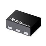
ICGOO电子元器件商城为您提供TPS62239DRYT由Texas Instruments设计生产,在icgoo商城现货销售,并且可以通过原厂、代理商等渠道进行代购。 TPS62239DRYT价格参考。Texas InstrumentsTPS62239DRYT封装/规格:PMIC - 稳压器 - DC DC 开关稳压器, 固定 降压 开关稳压器 IC 正 1V 1 输出 500mA 6-UFDFN。您可以下载TPS62239DRYT参考资料、Datasheet数据手册功能说明书,资料中有TPS62239DRYT 详细功能的应用电路图电压和使用方法及教程。
TPS62239DRYT 是 Texas Instruments(德州仪器)推出的一款高效同步降压转换器,属于 PMIC - 稳压器 - DC/DC 开关稳压器类别。它具有低静态电流和高效率的特点,适用于多种需要高性能电源管理的应用场景。以下是其主要应用场景:

1. 便携式电子设备
   TPS62239DRYT 适合用于电池供电的便携式设备,例如智能手机、平板电脑、可穿戴设备和便携式医疗设备。其高效的电源转换能力和低功耗特性能够延长电池寿命,同时为设备提供稳定的电压输出。

2. 物联网 (IoT) 设备
   在 IoT 领域中,TPS62239DRYT 可以为传感器节点、无线模块和其他低功耗设备供电。它的宽输入电压范围(2.5V 至 6V)和可调输出电压(0.8V 至 3.6V)使其能够适应不同的电源需求。

3. 嵌入式系统
   该芯片适用于工业自动化、通信设备和消费类电子产品中的嵌入式系统。它可以为微控制器、FPGA 和 DSP 提供稳定且高效的电源支持,确保系统的可靠运行。

4. 医疗设备
   在便携式医疗设备中,如血糖仪、脉搏血氧仪和便携式超声设备,TPS62239DRYT 的低噪声和高效率特性有助于提高设备性能并减少发热。

5. 汽车电子
   虽然 TPS62239DRYT 主要针对消费类和工业应用,但其宽电压范围和高可靠性也使其适合某些非关键性的汽车电子应用,例如车载信息娱乐系统或传感器模块。

6. 低功耗无线通信
   对于蓝牙、Wi-Fi 和 Zigbee 等低功耗无线通信模块,TPS62239DRYT 能够提供精确的电压调节,同时降低能耗,从而优化整体系统性能。

总之,TPS62239DRYT 凭借其高效能、小尺寸和灵活性,成为众多低功耗应用的理想选择,特别适合对电池寿命和系统稳定性有较高要求的场景。
| 参数 | 数值 |
| 产品目录 | 集成电路 (IC)半导体 |
| 描述 | IC REG BUCK SYNC 1V 0.5A 6SON稳压器—开关式稳压器 3MHz 500mA Step- Down Converter |
| 产品分类 | |
| 品牌 | Texas Instruments |
| 产品手册 | |
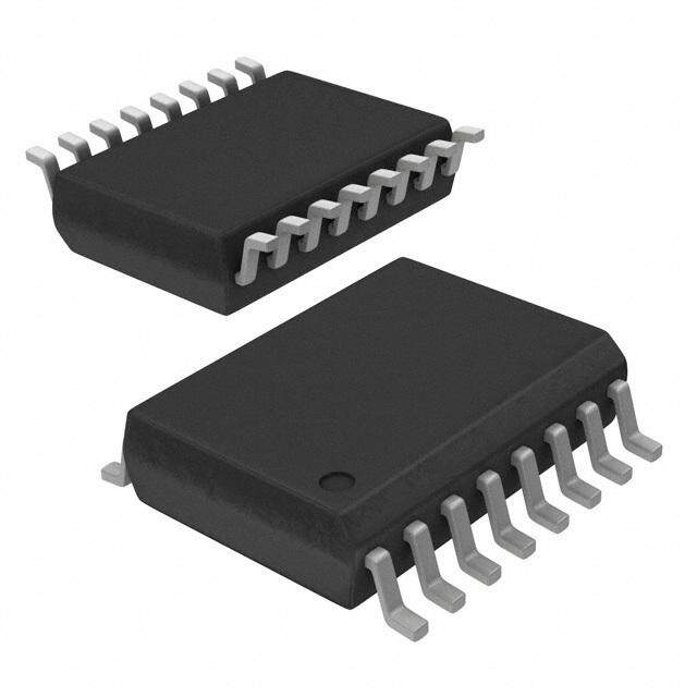
| 产品图片 |
|
| rohs | 符合RoHS无铅 / 符合限制有害物质指令(RoHS)规范要求 |
| 产品系列 | 电源管理 IC,稳压器—开关式稳压器,Texas Instruments TPS62239DRYT- |
| 数据手册 | |
| 产品型号 | TPS62239DRYT |
| PCN组件/产地 | |
| PWM类型 | 混合物 |
| 产品目录页面 | |
| 产品种类 | Controllers - DC/DC |
| 供应商器件封装 | 6-SON(1.45x1) |
| 其它名称 | 296-25326-1 |
| 包装 | 剪切带 (CT) |
| 同步整流器 | 是 |
| 商标 | Texas Instruments |
| 安装类型 | 表面贴装 |
| 安装风格 | SMD/SMT |
| 封装 | Reel |
| 封装/外壳 | 6-UFDFN |
| 封装/箱体 | USON-6 |
| 工作温度 | -40°C ~ 85°C |
| 工作温度范围 | - 40 C to + 85 C |
| 工厂包装数量 | 250 |
| 开关频率 | 2 MHz, 3 MHz |
| 拓扑结构 | Buck |
| 最大工作温度 | + 85 C |
| 最大输入电压 | 6 V |
| 最小工作温度 | - 40 C |
| 最小输入电压 | 2.05 V |
| 标准包装 | 1 |
| 电压-输入 | 2.05 V ~ 6 V |
| 电压-输出 | 1V |
| 电流-输出 | 500mA |
| 类型 | 降压(降压) |
| 系列 | TPS62239 |
| 输入电压 | 2.05 V to 6 V |
| 输出数 | 1 |
| 输出电压 | 1 V to 3.3 V |
| 输出电流 | 500 mA |
| 输出端数量 | 1 Output |
| 输出类型 | 固定 |
| 配用 | /product-detail/zh/TPS62239EVM-574/TPS62239EVM-574-ND/2353747 |
| 频率-开关 | 3MHz |


- 商务部:美国ITC正式对集成电路等产品启动337调查
- 曝三星4nm工艺存在良率问题 高通将骁龙8 Gen1或转产台积电
- 太阳诱电将投资9.5亿元在常州建新厂生产MLCC 预计2023年完工
- 英特尔发布欧洲新工厂建设计划 深化IDM 2.0 战略
- 台积电先进制程称霸业界 有大客户加持明年业绩稳了
- 达到5530亿美元!SIA预计今年全球半导体销售额将创下新高
- 英特尔拟将自动驾驶子公司Mobileye上市 估值或超500亿美元
- 三星加码芯片和SET,合并消费电子和移动部门,撤换高东真等 CEO
- 三星电子宣布重大人事变动 还合并消费电子和移动部门
- 海关总署:前11个月进口集成电路产品价值2.52万亿元 增长14.8%


PDF Datasheet 数据手册内容提取
Product Sample & Technical Tools & Support & Reference Folder Buy Documents Software Community Design TPS62230,TPS62231,TPS62232,TPS62233,TPS62234,TPS62235,TPS62236 TPS62237,TPS62238,TPS62239,TPS622310,TPS622311,TPS622312 TPS622313,TPS622314,TPS622315,TPS622316,TPS622317,TPS622318,TPS622319 SLVS941G–APRIL2009–REVISEDAUGUST2016 TPS6223xx 2-MHz and 3-MHz Ultra Small Step-Down Converter in 1 x 1.5 USON Package 1 Features With a wide input voltage range of 2.05 V to 6 V, the device supports applications powered by Li-Ion • 2MHz/3MHzSwitchingFrequency 1 batteries with extended voltage range. The minimum • Upto94%Efficiency input voltage of 2.05 V allows as well the operation • OutputPeakCurrentupto500mA from Li-primary or two alkaline batteries. Different fixed output voltage versions are available from 1.0 V • OperatingJunctionTemperatureof –40°Cto to3.3V. 125°C The TPS6223x series features switch frequency up to • HighPSRR(upto90dB) 3.8 MHz. At medium to heavy loads, the converter • SmallExternalOutputFilterComponents1 μH operates in pulse width modulation (PWM) mode and and4.7μF automatically enters power-save mode operation at • V rangefrom2.05Vto6V light load currents to maintain high efficiency over the IN • OptimizedPower-SaveModeforLowOutput entireloadcurrentrange. RippleVoltage Because of its excellent power supply rejection ratio • ForcedPWMModeOperation (PSRR) and AC load regulation performance, the device is also suitable to replace linear regulators to • Typ.22-μAQuiescentCurrent obtainbetterpowerconversionefficiency. • 100%DutyCycleforLowestDropout The power-save mode in TPS6223x reduces the • Small1-mm×1.5-mm × 0.6-mmUSONPackage quiescent current consumption down to 22 μA during • 12-mm2MinimumSolutionSize light load operation. It is optimized to achieve very • Supports0.6-mmMaximumSolutionHeight low output voltage ripple even with small external componentandfeaturesexcellentACloadregulation. 2 Applications For very noise-sensitive applications, the device can • LDOReplacement be forced to PWM mode operation over the entire load range by pulling the MODE pin high. In the • PortableAudio,PortableMedia shutdown mode, the current consumption is reduced • LowPowerWireless to less than 1 μA. The TPS6223x operates over a • LowPowerDSPCoreSupply junction temperature range of –40°C to 125°C. It is available in a 1 mm × 1.5 mm × 0.6 mm 6-pin SON • DigitalCameras package. 3 Description DeviceInformation(1) The TPS6223x device family is a high-frequency, PARTNUMBER PACKAGE BODYSIZE(NOM) synchronous, step-down DC – DC converter optimized for battery powered portable applications. It TPS6223xx USON(6) 1.45mmx1.00mm supports up to 500-mA output current and allows the (1) For all available packages, see the orderable addendum at use of tiny and low-cost chip inductors and theendofthedatasheet. capacitors. TypicalApplicationSchematic SmallPCBLayoutSize V L Total area 2.I0N5 V to 6 V TPS62231 1/2.2mH V L1 is less than VIN SW OUT 1.8 V 12mm² CIN EN FB COUT V 2.2mF MODE GND 4.7mF IN C Copyright © 2016, Texas Instruments Incorporated 1 C2 GND V OUT 1 An IMPORTANT NOTICE at the end of this data sheet addresses availability, warranty, changes, use in safety-critical applications, intellectualpropertymattersandotherimportantdisclaimers.PRODUCTIONDATA.
TPS62230,TPS62231,TPS62232,TPS62233,TPS62234,TPS62235,TPS62236 TPS62237,TPS62238,TPS62239,TPS622310,TPS622311,TPS622312 TPS622313,TPS622314,TPS622315,TPS622316,TPS622317,TPS622318,TPS622319 SLVS941G–APRIL2009–REVISEDAUGUST2016 www.ti.com Table of Contents 1 Features.................................................................. 1 9 ApplicationandImplementation........................ 13 2 Applications........................................................... 1 9.1 ApplicationInformation............................................13 3 Description............................................................. 1 9.2 TypicalApplication..................................................13 4 RevisionHistory..................................................... 2 9.3 SystemExamples...................................................26 5 DeviceComparisonTable..................................... 4 10 PowerSupplyRecommendations..................... 27 6 PinConfigurationandFunctions......................... 5 11 Layout................................................................... 27 11.1 LayoutGuidelines.................................................27 7 Specifications......................................................... 5 11.2 LayoutExample....................................................27 7.1 AbsoluteMaximumRatings......................................5 12 DeviceandDocumentationSupport................. 28 7.2 ESDRatings..............................................................5 7.3 RecommendedOperatingConditions.......................6 12.1 DeviceSupport......................................................28 7.4 ThermalInformation..................................................6 12.2 RelatedLinks........................................................28 7.5 ElectricalCharacteristics...........................................7 12.3 ReceivingNotificationofDocumentationUpdates28 7.6 TypicalCharacteristics..............................................8 12.4 CommunityResources..........................................29 12.5 Trademarks...........................................................29 8 DetailedDescription.............................................. 9 12.6 ElectrostaticDischargeCaution............................29 8.1 Overview...................................................................9 12.7 Glossary................................................................29 8.2 FunctionalBlockDiagram.......................................10 13 Mechanical,Packaging,andOrderable 8.3 FeatureDescription.................................................10 Information........................................................... 29 8.4 DeviceFunctionalModes........................................11 4 Revision History NOTE:Pagenumbersforpreviousrevisionsmaydifferfrompagenumbersinthecurrentversion. ChangesfromRevisionF(July2015)toRevisionG Page • AddeddeviceTPS622319 ..................................................................................................................................................... 4 • DeletedPackageinformationfromDeviceComparisonTable,andaddedfootnote ............................................................ 4 • AddedReceivingNotificationofDocumentationUpdatessection....................................................................................... 28 ChangesfromRevisionE(December2010)toRevisionF Page • AddedPinConfigurationandFunctionssection,ESDRatingstable,FeatureDescriptionsection,DeviceFunctional Modes,ApplicationandImplementationsection,PowerSupplyRecommendationssection,Layoutsection,Device andDocumentationSupportsection,andMechanical,Packaging,andOrderableInformationsection .............................. 1 ChangesfromRevisionD(August2010)toRevisionE Page • AddeddevicenumberTPS622318......................................................................................................................................... 1 ChangesfromRevisionC(April2010)toRevisionD Page • AddeddevicenumbersTPS622315,TPS622316,andTPS622317...................................................................................... 1 • Changeddatasheetstatusfrom"ProductMix"to"ProductionData".................................................................................... 1 • Deletedtablefootnoteregarding"othervoltageoptions"....................................................................................................... 4 ChangesfromRevisionB(December2009)toRevisionC Page • AddeddevicenumbersTPS622312,TPS622313,andTPS622314...................................................................................... 1 2 SubmitDocumentationFeedback Copyright©2009–2016,TexasInstrumentsIncorporated ProductFolderLinks:TPS62230TPS62231 TPS62232 TPS62233 TPS62234 TPS62235 TPS62236 TPS62237 TPS62238 TPS62239 TPS622310 TPS622311 TPS622312TPS622313 TPS622314 TPS622315 TPS622316 TPS622317 TPS622318 TPS622319
TPS62230,TPS62231,TPS62232,TPS62233,TPS62234,TPS62235,TPS62236 TPS62237,TPS62238,TPS62239,TPS622310,TPS622311,TPS622312 TPS622313,TPS622314,TPS622315,TPS622316,TPS622317,TPS622318,TPS622319 www.ti.com SLVS941G–APRIL2009–REVISEDAUGUST2016 ChangesfromRevisionA(August2009)toRevisionB Page • AddeddevicenumbersTPS62235,TPS62236,TPS62237,TPS622311.............................................................................. 1 • ChangedtheTitleFrom:3MHzUltraSmallStepDownConverterin1x1.5SONPackageTo:2MHz/3MHzUltra SmallStepDownConverterin1x1.5SONPackage.............................................................................................................. 1 • ChangedFeature:From:3MHzswitchfrequencyTo:2MHz/3MHzswitchfrequency..................................................... 1 • AddedFigure6,Figure7,andFigure10............................................................................................................................. 16 • AddedFigure15................................................................................................................................................................... 17 • AddedFigure24,andFigure25........................................................................................................................................... 19 • AddedFigure32................................................................................................................................................................... 21 • AddedFigure41,andFigure42........................................................................................................................................... 23 ChangesfromOriginal(April2009)toRevisionA Page • AddeddevicenumbersTPS62233,TPS62234,TPS62238,TPS62239,andTPS622310tothedatasheet....................... 1 Copyright©2009–2016,TexasInstrumentsIncorporated SubmitDocumentationFeedback 3 ProductFolderLinks:TPS62230TPS62231 TPS62232 TPS62233 TPS62234 TPS62235 TPS62236 TPS62237 TPS62238 TPS62239 TPS622310 TPS622311 TPS622312TPS622313 TPS622314 TPS622315 TPS622316 TPS622317 TPS622318 TPS622319
TPS62230,TPS62231,TPS62232,TPS62233,TPS62234,TPS62235,TPS62236 TPS62237,TPS62238,TPS62239,TPS622310,TPS622311,TPS622312 TPS622313,TPS622314,TPS622315,TPS622316,TPS622317,TPS622318,TPS622319 SLVS941G–APRIL2009–REVISEDAUGUST2016 www.ti.com 5 Device Comparison Table PARTNUMBER(1) OUTPUTVOLTAGE FREQUENCY Pulldown PACKAGE [MHz] EN,MODE MARKING TPS62230 2.5V 3 no GV TPS62231 1.8V 3 no GW TPS62232 1.2V 3 no GX TPS62239 1.0V 3 no OP TPS622311 1.1V 2 no PA TPS622315 1.15V 2 no RI TPS62235 1.2V 2 no OQ TPS622318 1.25V 3 no ST TPS622319 1.2V 2 yes 3O TPS622313 1.3V 3 no QF TPS622314 1.5V 3 no QG TPS62236 1.85V 2 no OR TPS622312 2.0V 3 no QE TPS62234 2.1V 3 no OH TPS62238 2.25V 3 no ON TPS622310 2.3V 3 no OT TPS622316 2.7V 3 no RJ TPS622317 2.9V 3 no RK TPS62233 3.0V 3 no OG TPS62237 3.3V 2 no OS (1) FordetailedorderinginformationseethePACKAGEOPTIONADDENDUMattheendofthisdatasheet. 4 SubmitDocumentationFeedback Copyright©2009–2016,TexasInstrumentsIncorporated ProductFolderLinks:TPS62230TPS62231 TPS62232 TPS62233 TPS62234 TPS62235 TPS62236 TPS62237 TPS62238 TPS62239 TPS622310 TPS622311 TPS622312TPS622313 TPS622314 TPS622315 TPS622316 TPS622317 TPS622318 TPS622319
TPS62230,TPS62231,TPS62232,TPS62233,TPS62234,TPS62235,TPS62236 TPS62237,TPS62238,TPS62239,TPS622310,TPS622311,TPS622312 TPS622313,TPS622314,TPS622315,TPS622316,TPS622317,TPS622318,TPS622319 www.ti.com SLVS941G–APRIL2009–REVISEDAUGUST2016 6 Pin Configuration and Functions DRYPackage 6-PinUSON TopView MODE 1 6 FB SW 2 5 EN VIN 3 4 GND PinFunctions PIN TYPE DESCRIPTION NAME NO VIN 3 Power V powersupplypin IN GND 4 Power GNDsupplypin EN 5 Input Thisistheenablepinofthedevice.Pullingthispintolowforcesthedeviceintoshutdownmode. Pullingthispintohighenablesthedevice.Thispinmustbeterminatedexceptforthe TPS622319,whichhasanintegrated1MΩalwaysactivepull-downresistor. SW 2 Output ThisistheswitchpinandisconnectedtotheinternalMOSFETswitches.Connecttheinductorto thisterminal FB 6 Input Feedbackpinfortheinternalregulationloop.Connectthispindirectlytotheoutputcapacitor. MODE 1 Input MODEpin=HighforcesthedevicetooperateinPWMmode.Mode=Lowenablesthepower savemodewithautomatictransitionfrompulsefrequencymodulation(PFM)topulsewidth modulation(PWM)mode.ThispinmustbeterminatedexceptfortheTPS622319,whichhasan integrated1MΩalwaysactivepull-downresistor. 7 Specifications 7.1 Absolute Maximum Ratings overoperatingfree-airtemperaturerange(unlessotherwisenoted)(1) MIN MAX UNIT VoltageatVINandSWpin(2) –0.3 7 V V VoltageatEN,MODEpin(2) –0.3 V +0.3,≤7 V IN IN VoltageatFBpin(2) –0.3 3.6 V Peakoutputcurrent Internallylimited A Powerdissipation Internallylimited T OperatingjunctionTemperatureRange –40 150 °C J T StorageTemperatureRange –65 150 °C stg (1) StressesbeyondthoselistedunderAbsoluteMaximumRatingsmaycausepermanentdamagetothedevice.Thesearestressratings onlyandfunctionaloperationofthedeviceattheseoranyotherconditionsbeyondthoseindicatedunderRecommendedOperating Conditionsisnotimplied.Exposuretoabsolute–maximum–ratedconditionsforextendedperiodsmayaffectdevicereliability. (2) Allvoltagevaluesarewithrespecttonetworkgroundterminal. 7.2 ESD Ratings VALUE UNIT Humanbodymodel(HBM),perANSI/ESDA/JEDECJS-001,all pins(1) ±2000 V Electrostaticdischarge V (ESD) Charge-devicemodel(CDM),perJEDECspecificationJESD22- C101,allpins(2) ±1000 (1) JEDECdocumentJEP155statesthat500-VHBMallowssafemanufacturingwithastandardESDcontrolprocess. (2) JEDECdocumentJEP157statesthat250-VCDMallowssafemanufacturingwithastandardESDcontrolprocess. Copyright©2009–2016,TexasInstrumentsIncorporated SubmitDocumentationFeedback 5 ProductFolderLinks:TPS62230TPS62231 TPS62232 TPS62233 TPS62234 TPS62235 TPS62236 TPS62237 TPS62238 TPS62239 TPS622310 TPS622311 TPS622312TPS622313 TPS622314 TPS622315 TPS622316 TPS622317 TPS622318 TPS622319
TPS62230,TPS62231,TPS62232,TPS62233,TPS62234,TPS62235,TPS62236 TPS62237,TPS62238,TPS62239,TPS622310,TPS622311,TPS622312 TPS622313,TPS622314,TPS622315,TPS622316,TPS622317,TPS622318,TPS622319 SLVS941G–APRIL2009–REVISEDAUGUST2016 www.ti.com 7.3 Recommended Operating Conditions overoperatingjunctiontemperaturerange(unlessotherwisenoted)(1) MIN NOM MAX UNIT SupplyvoltageV (2) 2.05 6 V IN Effectiveinductance 2.2 μH Effectivecapacitance 2 4.7 μF V ≤V –1V(3) 500mAmaximumI (4) 3 3.6 OUT IN OUT Recommendedminimum 350mAmaximumI (4) 2.5 2.7 V supplyvoltage OUT V ≤1.8V 60mAmaximumoutputcurrent(4) 2.05 OUT Operatingjunctiontemperature,T –40 125 °C J (1) Inapplicationswherehighpowerdissipationand/orpoorpackagethermalresistanceispresent,themaximumambienttemperaturemay havetobederated.Maximumambienttemperature(T )isdependentonthemaximumoperatingjunctiontemperature(T ),the A(max) J(max) maximumpowerdissipationofthedeviceintheapplication(P ),andthejunction-to-ambientthermalresistanceofthepart/package D(max) intheapplication(R ),asgivenbythefollowingequation:T =T –(R ×P ). θJA A(max) J(max) θJA D(max) (2) Theminimumrequiredsupplyvoltageforstartupis2.05V.Thepartisfunctionaldowntothefallingundervoltagelockout(UVL) threshold. (3) ForavoltagedifferencebetweenminimumV andV of≥1V IN OUT (4) TypicalvalueappliesforT =25°C,maximumvalueappliesforT ≤125°C,PCBlayoutmustsupportproperthermalperformance. A J 7.4 Thermal Information TPS6223x THERMALMETRIC(1) DRY(USON) UNIT 6PINS R Junction-to-ambientthermalresistance 294.5 °C/W θJA R Junction-to-case(top)thermalresistance 166.5 °C/W θJC(top) R Junction-to-boardthermalresistance 166.1 °C/W θJB ψ Junction-to-topcharacterizationparameter 27.3 °C/W JT ψ Junction-to-boardcharacterizationparameter 159.9 °C/W JB R Junction-to-case(bottom)thermalresistance — °C/W θJC(bot) (1) Formoreinformationabouttraditionalandnewthermalmetrics,seetheSemiconductorandICPackageThermalMetricsapplication report,SPRA953. 6 SubmitDocumentationFeedback Copyright©2009–2016,TexasInstrumentsIncorporated ProductFolderLinks:TPS62230TPS62231 TPS62232 TPS62233 TPS62234 TPS62235 TPS62236 TPS62237 TPS62238 TPS62239 TPS622310 TPS622311 TPS622312TPS622313 TPS622314 TPS622315 TPS622316 TPS622317 TPS622318 TPS622319
TPS62230,TPS62231,TPS62232,TPS62233,TPS62234,TPS62235,TPS62236 TPS62237,TPS62238,TPS62239,TPS622310,TPS622311,TPS622312 TPS622313,TPS622314,TPS622315,TPS622316,TPS622317,TPS622318,TPS622319 www.ti.com SLVS941G–APRIL2009–REVISEDAUGUST2016 7.5 Electrical Characteristics V =3.6V,V =1.8V,EN=V ,MODE=GND,T =–40°Cto125°CtypicalvaluesareatT =25°C(unlessotherwise IN OUT IN J J noted),C =2.2μF,L=2.2μH,C =4.7μF.(1) IN OUT PARAMETER TESTCONDITIONS MIN TYP MAX UNIT SUPPLY V Inputvoltage(2) 2.05 6 V IN PFMoperation(MODE=GND),I =0mA, OUT 22 40 μA devicenotswitching,T =–40°Cto85°C J PFMoperation(MODE=GND),I =0mA, I Operatingquiescentcurrent OUT 25 μA Q deviceswitching,V =1.2V OUT PWMoperation(MODE=V ),I =0mA,device IN OUT 3 mA switching I Shutdowncurrent EN=GND,T =–40°Cto85°C 0.1 1 μA SD J Falling 1.8 1.9 V V Undervoltagelockoutthreshold UVLO Rising 1.9 2.05 V ENABLE,MODETHRESHOLD V ThresholdfordetectinghighEN,MODE 2.05V≤V ≤6V,risingedge 0.8 1 V IHTH IN V ThresholdfordetectinglowEN,MODE 2.05V≤V ≤6V,fallingedge,T =–40°Cto ILTHHYS IN J 0.4 0.6 V 85°C R Pull-downresistorEN,MODE TPS622319 1 MΩ pd I Inputbiascurrent,EN,MODE EN,MODE=GNDorV ,T =–40°Cto85°C, IN IN J 0.01 0.5 μA exceptTPS622319 POWERSWITCH HighsideMOSFETON-resistance 600 850 R V =3.6V,T =–40°Cto85°C mΩ DS(ON) IN J LowSideMOSFETON-resistance 350 480 ForwardcurrentlimitMOSFEThigh- 690 850 1050 mA I side V =3.6V,open-loop LIMF IN ForwardcurrentlimitMOSFETlow-side 550 840 1220 mA T Thermalshutdown Increasingjunctiontemperature 150 °C JSD Thermalshutdownhysteresis Decreasingjunctiontemperature 20 °C CONTROLLER t MinimumON-time MODE=V ,I =0mA 135 ns ONmin IN OUT t MinimumOFF-time 40 ns OFFmin OUTPUT V Internalreferencevoltage 0.7 V REF MODE=GND,I =0mA 0% OUT Outputvoltageaccuracy(3) MODE=V ,I =0mA T =25°C –2% 2% IN OUT J V T =–40°Cto125°C –2.5% 2.5% OUT J DCoutputvoltageloadregulation MODE=V 0.001 %/mA IN DCoutputvoltagelineregulation MODE=V ,I =0mA,2.05V≤V ≤6V 0 %/V IN OUT IN t Start-uptime TimefromactiveENtoV =1.8V,10-Ωload 100 μs Start OUT I LeakagecurrentintoSWpin V =V =V =3.6V,EN=GND(4),T = LK_SW IN OUT SW J 0.1 0.5 μA –40°Cto85°C (1) Inapplicationswherehighpowerdissipationand/orpoorpackagethermalresistanceispresent,themaximumambienttemperaturemay havetobederated.Maximumambienttemperature(T )isdependentonthemaximumoperatingjunctiontemperature(T ),the A(max) J(max) maximumpowerdissipationofthedeviceintheapplication(PD(max)),andthejunction-to-ambientthermalresistanceofthe part/packageintheapplication(R ),asgivenbythefollowingequation:T =T –(R ×P ). θJA A(max) J(max) θJA D(max) (2) Theminimumrequiredsupplyvoltageforstartupis2.05V.Thepartisfunctionaldowntothefallingundervoltagelockout(UVL) threshold. (3) V =V +1.0V IN O (4) TheinternalresistordividernetworkisdisconnectedfromFBpin. Copyright©2009–2016,TexasInstrumentsIncorporated SubmitDocumentationFeedback 7 ProductFolderLinks:TPS62230TPS62231 TPS62232 TPS62233 TPS62234 TPS62235 TPS62236 TPS62237 TPS62238 TPS62239 TPS622310 TPS622311 TPS622312TPS622313 TPS622314 TPS622315 TPS622316 TPS622317 TPS622318 TPS622319
TPS62230,TPS62231,TPS62232,TPS62233,TPS62234,TPS62235,TPS62236 TPS62237,TPS62238,TPS62239,TPS622310,TPS622311,TPS622312 TPS622313,TPS622314,TPS622315,TPS622316,TPS622317,TPS622318,TPS622319 SLVS941G–APRIL2009–REVISEDAUGUST2016 www.ti.com 7.6 Typical Characteristics 35 0.2 TA= 85°C 0.18 TA= 85°C 30 TA= 60°C TA= 25°C 0.16 A A nt -m nt -m 0.14 urre 25 urre 0.12 C C Quiescent 20 TA= -40°C Shutdown 0.00.81 TA= 60°C TA= 25°C TA= -40°C I- Q15 I- SD 00..0046 0.02 10 0 2 2.5 3 3.5 4 4.5 5 5.5 6 2 2.5 3 3.5 4 4.5 5 5.5 6 VIN- Input Voltage - V VIN- Input Voltage - V Figure1.QuiescentCurrentIQvsAmbientTemperatureTA Figure2.ShutdownCurrentISDvsAmbientTemperatureTA W 2 W 0.7 e - PMOS e - NMOS esistanc 11..68 TA= T8A5°=C 60°C esistanc 0.6 TA= 85°TCA= 60°C R R On-State 11..24 TA= 25T°AC= -40°C On-State 00..45 TA= 25T°AC= -40°C Source 0.81 Source 0.3 Drain- 0.6 Drain- 0.2 r- Static DS(ON)00..0242 2.5 3 3.5 4 4.5 5 5.5 6 r- Static DS(ON) 0.012 2.5 3 3.5 4 4.5 5 5.5 6 VIN- Input Voltage - V VIN- Input Voltage - V Figure3.PMOSRDSONvsSupplyVoltageVINandAmbient Figure4.NMOSRDSONvsSupplyVoltageVINandAmbient TemperatureTA TemperatureTA 8 SubmitDocumentationFeedback Copyright©2009–2016,TexasInstrumentsIncorporated ProductFolderLinks:TPS62230TPS62231 TPS62232 TPS62233 TPS62234 TPS62235 TPS62236 TPS62237 TPS62238 TPS62239 TPS622310 TPS622311 TPS622312TPS622313 TPS622314 TPS622315 TPS622316 TPS622317 TPS622318 TPS622319
TPS62230,TPS62231,TPS62232,TPS62233,TPS62234,TPS62235,TPS62236 TPS62237,TPS62238,TPS62239,TPS622310,TPS622311,TPS622312 TPS622313,TPS622314,TPS622315,TPS622316,TPS622317,TPS622318,TPS622319 www.ti.com SLVS941G–APRIL2009–REVISEDAUGUST2016 8 Detailed Description 8.1 Overview The TPS6223x synchronous step-down DC – DC converter family includes a unique hysteretic PWM controller scheme which enables switch frequencies over 3 MHz, excellent transient and AC load regulation as well as operationwithcost-competitiveexternalcomponents. The controller topology supports forced PWM mode as well as power-save mode operation. Power-save mode operation reduces the quiescent current consumption down to 22 μA and ensures high conversion efficiency at light loads by skipping switch pulses. In forced PWM mode, the device operates on a quasi-fixed frequency, avoidspulseskipping,andallowsfilteringoftheswitchnoisebyexternalfiltercomponents. The TPS6223x devices offer fixed output voltage options featuring smallest solution size by using only three externalcomponents. The internal switch current limit of typical 850 mA supports output currents of up to 500 mA, depending on the operatingcondition. A significant advantage of TPS6223x compared to other hysteretic PWM controller topologies is its excellent DC and AC load regulation capability in combination with low-output voltage ripple over the entire load range which makesthispartwellsuitedforaudioandRFapplications. Once the output voltage falls below the threshold of the error comparator, a switch pulse is initiated, and the high-side switch is turned on. It remains turned on until a minimum ON-time of t expires and the output ONmin voltage trips the threshold of the error comparator or the inductor current reaches the high-side switch current limit. Once the high-side switch turns off, the low-side switch rectifier is turned on and the inductor current ramps downuntilthehigh-sideswitchturnsonagainortheinductorcurrentreacheszero. In forced PWM mode operation, negative inductor current is allowed to enable continuous conduction mode even atnoloadcondition. Copyright©2009–2016,TexasInstrumentsIncorporated SubmitDocumentationFeedback 9 ProductFolderLinks:TPS62230TPS62231 TPS62232 TPS62233 TPS62234 TPS62235 TPS62236 TPS62237 TPS62238 TPS62239 TPS622310 TPS622311 TPS622312TPS622313 TPS622314 TPS622315 TPS622316 TPS622317 TPS622318 TPS622319
TPS62230,TPS62231,TPS62232,TPS62233,TPS62234,TPS62235,TPS62236 TPS62237,TPS62238,TPS62239,TPS622310,TPS622311,TPS622312 TPS622313,TPS622314,TPS622315,TPS622316,TPS622317,TPS622318,TPS622319 SLVS941G–APRIL2009–REVISEDAUGUST2016 www.ti.com 8.2 Functional Block Diagram VIN VREF Undervoltage Current Bandgap 0.70 V Lockout Limit Comparator Limit High Side MODE MODE PMOS Softstart VIN Gate Driver Min. OnTime Control Anti SW EN FB Logic Shoot-Through Min. OFFTime VREF NMOS FB Limit Low Side Integrated Feed Back Error Thermal Zero/Negative Network Comparator Shutdown Current Limit Comparator EN GND Copyright © 2016, Texas Instruments Incorporated 8.3 Feature Description 8.3.1 UndervoltageLockout The undervoltage lockout circuit prevents the device from misoperation at low input voltages. It prevents the converter from turning on the switch or rectifier MOSFET under undefined conditions. The TPS6223x devices have a UVLO threshold set to 1.8 V (typical). Fully functional operation is permitted for input voltage down to the falling UVLO threshold level. The converter starts operation again once the input voltage trips the rising UVLO thresholdlevel. 8.3.2 EnableandShutdown The device starts operation when EN is set high and starts up with the soft-start as previously described. For proper operation, the EN pin must be terminated and must not be left floating, except for the TPS622319, which hasanintegrated1MΩalwaysactivepull-downresistor. Pulling the EN pin low forces the device into shutdown, with a shutdown quiescent current of typically 0.1 μA. In this mode, the P- and N-channel MOSFETs are turned off, the internal resistor feedback divider is disconnected, andtheentireinternal-controlcircuitryisswitchedoff. The EN input can be used to control power sequencing in a system with various DC – DC converters. The EN pin can be connected to the output of another converter, to drive the EN pin high and getting a sequencing of supplyrails. 8.3.3 ThermalShutdown As soon as the junction temperature, T , exceeds 150°C (typical) the device goes into thermal shutdown. In this J mode, the high-side and low-side MOSFETs are turned off. The device continues its operation when the junction temperaturefallsbelowthethermalshutdownhysteresis. 10 SubmitDocumentationFeedback Copyright©2009–2016,TexasInstrumentsIncorporated ProductFolderLinks:TPS62230TPS62231 TPS62232 TPS62233 TPS62234 TPS62235 TPS62236 TPS62237 TPS62238 TPS62239 TPS622310 TPS622311 TPS622312TPS622313 TPS622314 TPS622315 TPS622316 TPS622317 TPS622318 TPS622319
TPS62230,TPS62231,TPS62232,TPS62233,TPS62234,TPS62235,TPS62236 TPS62237,TPS62238,TPS62239,TPS622310,TPS622311,TPS622312 TPS622313,TPS622314,TPS622315,TPS622316,TPS622317,TPS622318,TPS622319 www.ti.com SLVS941G–APRIL2009–REVISEDAUGUST2016 8.4 Device Functional Modes 8.4.1 Soft-Start The TPS6223x has an internal soft start circuit that controls the ramp up of the output voltage and limits the inrush current during start-up. This limits input voltage drops when a battery or a high-impedance power source isconnectedtotheinputoftheconverter. The soft-start system generates a monotonic ramp up of the output voltage and reaches the nominal output voltagetypically100μsafterENpinwaspulledhigh. If the output voltage does not reached its target value by this time, such as in the case of heavy load, the converterthenoperatesinacurrentlimitmodesetbyitsswitchcurrentlimits. TPS6223x is able to start into a prebiased output capacitor. The converter starts with the applied bias voltage andrampstheoutputvoltagetoitsnominalvalue. 8.4.2 Power-SaveMode Connecting the MODE pin to GND enables the automatic PWM and power-save mode operation. The converter operates in quasi-fixed frequency PWM mode at moderate to heavy loads and in the pulse frequency modulation (PFM)modeduringlightloads,whichmaintainshighefficiencyoverawideloadcurrentrange.InPFMmode,the device starts to skip switch pulses and generates only single pulses with an ON-time of t . The PFM mode ONmin frequency depends on the load current and the external inductor and output capacitor values. The PFM mode of TPS6223x is optimized for low-output voltage ripple if small external components are used. Even at low output currents, the PFM frequency is above the audible noise spectrum and makes this operation mode suitable for audioapplications. TheON-timet canbeestimatedto: ONmin V t = OUT ´ 260ns ONmin V IN (1) Therefore,thepeakinductorcurrentinPFMmodeisapproximately: (V - V ) I = IN OUT ´ t LPFMpeak ONmin L (2) ThetransitionfromPFMintoPWMmodeandviceversacanbeestimatedto: I = 0.5 x I OUT_PFM/PWM LPFMpeak where • t :High-sideswitchON-time[ns] ON • V :Inputvoltage[V] IN • V :Outputvoltage[V] OUT • L:Inductance[μH] • I :PFMinductorpeakcurrent[mA] LPFMpeak • I :OutputcurrentforPFMtoPWMmodetransitionandviceversa[mA] (3) OUT_PFM/PWM 8.4.3 ForcedPWMMode Pulling the MODE pin high forces the converter to operate in a continuous conduction PWM mode even at light load currents. The advantage is that the converter operates with a quasi-fixed frequency that allows simple filtering of the switching frequency for noise-sensitive applications. In this mode, the efficiency is lower compared to the power save mode during light loads. This pin must be terminated except for the TPS622319 , which has anintegrated1MΩ alwaysactivepull-downresistor. For additional flexibility, it is possible to switch from power-save mode to forced PWM mode during operation. This allows efficient power management by adjusting the operation of the converter to the specific system requirements. Copyright©2009–2016,TexasInstrumentsIncorporated SubmitDocumentationFeedback 11 ProductFolderLinks:TPS62230TPS62231 TPS62232 TPS62233 TPS62234 TPS62235 TPS62236 TPS62237 TPS62238 TPS62239 TPS622310 TPS622311 TPS622312TPS622313 TPS622314 TPS622315 TPS622316 TPS622317 TPS622318 TPS622319
TPS62230,TPS62231,TPS62232,TPS62233,TPS62234,TPS62235,TPS62236 TPS62237,TPS62238,TPS62239,TPS622310,TPS622311,TPS622312 TPS622313,TPS622314,TPS622315,TPS622316,TPS622317,TPS622318,TPS622319 SLVS941G–APRIL2009–REVISEDAUGUST2016 www.ti.com Device Functional Modes (continued) 8.4.4 100%DutyCycleLowDropoutOperation The device starts to enter 100% duty cycle mode once the input voltage comes close to the nominal output voltage.Tomaintaintheoutputvoltage,thehighsideswitchisturnedon100%foroneormorecycles. With further decreasing V the high-side MOSFET switch is turned on completely. In this case the converter IN offers a low input-to-output voltage difference. This is particularly useful in battery-powered applications to achievelongestoperationtimebytakingfulladvantageofthewholebatteryvoltagerange. The minimum input voltage to maintain regulation depends on the load current and output voltage, and can be calculatedas: ( ) V min=V max+I max ´ R max+R IN OUT OUT DS(on) L where • I max:maximumoutputcurrentplusinductorripplecurrent OUT • R max:maximumP-channelswitchRDSon DS(on) • R :DCresistanceoftheinductor L • V max:nominaloutputvoltageplusmaximumoutputvoltagetolerance (4) OUT 8.4.5 ShortCircuitProtection The TPS6223x integrates a high-side and low-side MOSFET current limit to protect the device against heavy load or short circuit. The current in the switches is monitored by current limit comparators. When the current in the P-channel MOSFET reaches its current limit, the P-channel MOSFET is turned off and the N-channel MOSFET is turned on to ramp down the current in the inductor. The high-side MOSFET switch can only turn on again, once the current in the low side MOSFET switch has decreased below the threshold of its current limit comparator. 12 SubmitDocumentationFeedback Copyright©2009–2016,TexasInstrumentsIncorporated ProductFolderLinks:TPS62230TPS62231 TPS62232 TPS62233 TPS62234 TPS62235 TPS62236 TPS62237 TPS62238 TPS62239 TPS622310 TPS622311 TPS622312TPS622313 TPS622314 TPS622315 TPS622316 TPS622317 TPS622318 TPS622319
TPS62230,TPS62231,TPS62232,TPS62233,TPS62234,TPS62235,TPS62236 TPS62237,TPS62238,TPS62239,TPS622310,TPS622311,TPS622312 TPS622313,TPS622314,TPS622315,TPS622316,TPS622317,TPS622318,TPS622319 www.ti.com SLVS941G–APRIL2009–REVISEDAUGUST2016 9 Application and Implementation NOTE Information in the following applications sections is not part of the TI component specification, and TI does not warrant its accuracy or completeness. TI’s customers are responsible for determining suitability of components for their purposes. Customers should validateandtesttheirdesignimplementationtoconfirmsystemfunctionality. 9.1 Application Information The TPS6223x device family are high-frequency, synchronous, step-down DC-DC converters providing switch frequenciesupto3.8MHz.Differentfixedoutputvoltageversionsareavailablefrom1.0Vto3.3V. 9.2 Typical Application L V IN TPS62230 1/2.2mH 2.7 V to 6 V VOUT VIN SW 2.5 V EN FB CIN MODE GND COUT 2.2mF 4.7mF Copyright © 2016, Texas Instruments Incorporated Figure5. TPS622302.5-VOutput 9.2.1 DesignRequirements The device operates over an input voltage range from 2.05 V to 6 V. The device family offers a broad range of internally fixed output voltage options from 1 V to 3.3 V. The TPS6223x is easy to use and needs just three external components; however, the selection of external components and PCB layout must comply with the designguidelinestoachievespecifiedperformance. 9.2.2 DetailedDesignProcedure 9.2.2.1 OutputFilterDesign(InductorandOutputCapacitor) The TPS6223x is optimized to operate with effective inductance values in the range of 0.7 μH to 4.3 μH and with effective output capacitance in the range of 2.0 μF to 15 μF. The internal compensation is optimized to operate with an output filter of L = 1.0 μH/2.2 μH and C = 4.7 μF. Larger or smaller inductor/capacitor values can be OUT used to optimize the performance of the device for specific operation conditions. For more details, see the CheckingLoopStabilitysection. Copyright©2009–2016,TexasInstrumentsIncorporated SubmitDocumentationFeedback 13 ProductFolderLinks:TPS62230TPS62231 TPS62232 TPS62233 TPS62234 TPS62235 TPS62236 TPS62237 TPS62238 TPS62239 TPS622310 TPS622311 TPS622312TPS622313 TPS622314 TPS622315 TPS622316 TPS622317 TPS622318 TPS622319
TPS62230,TPS62231,TPS62232,TPS62233,TPS62234,TPS62235,TPS62236 TPS62237,TPS62238,TPS62239,TPS622310,TPS622311,TPS622312 TPS622313,TPS622314,TPS622315,TPS622316,TPS622317,TPS622318,TPS622319 SLVS941G–APRIL2009–REVISEDAUGUST2016 www.ti.com Typical Application (continued) 9.2.2.2 InductorSelection The inductor value affects its peak-to-peak ripple current, the PWM-to-PFM transition point, the output voltage ripple and the efficiency. The selected inductor has to be rated for its DC resistance and saturation current. The inductor ripple current (ΔI ) decreases with higher inductance and increases with higher V or V . Equation 5 L IN OUT calculates the maximum inductor current under static load conditions. The saturation current of the inductor must be rated higher than the maximum inductor current as calculated with Equation 6. This is recommended because duringheavyloadtransienttheinductorcurrentwillriseabovethecalculatedvalue. Vout 1- Vin DI =Vout ´ L L ´ ¦ (5) DI I =I + L Lmax outmax 2 where • f=Switchingfrequency • L=Inductorvalue • ΔI =Peak-to-peakinductorripplecurrent L • I =Maximuminductorcurrent (6) Lmax In high-frequency converter applications, the efficiency is essentially affected by the inductor AC resistance (that is, quality factor) and to a smaller extent by the inductor DCR value. To achieve high-efficiency operation, take care in selecting inductors featuring a quality factor above 25 at the switching frequency. Increasing the inductor value produces lower RMS currents, but degrades transient response. For a given physical inductor size, increasedinductanceusuallyresultsinaninductorwithlowersaturationcurrent. The total losses of the coil consist of both the losses in the DC resistance, R , and the following frequency- (DC) dependentcomponents: • Thelossesinthecorematerial(magnetichysteresisloss,especiallyathighswitchingfrequencies) • Additionallossesintheconductorfromtheskineffect(currentdisplacementathighfrequencies) • Magneticfieldlossesoftheneighboringwindings(proximityeffect) • Radiationlosses ThefollowinginductorseriesfromdifferentsuppliershavebeenusedwiththeTPS6223xconverters. Table1.ListofInductors INDUCTANCE DIMENSIONS INDUCTORTYPE SUPPLIER(1) (μH) (mm3) 1.0/2.2 2.5×2.0×1.2 LQM2HPN1R0MJ0 Murata 2.2 2.0×1.2×0.55 LQM21PN2R2 Murata 1.0/2.2 2.0×1.2×1.0 MIPSZ2012 FDK 1.0/2.2 2.0×2.5×1.2 MIPSA2520 FDK 1.0/2.2 2.0×1.2×1.0 KSLI2012series HitachiMetal (1) SeeThird-PartyProductsDisclaimer 9.2.2.3 OutputCapacitorSelection The unique hysteretic PWM control scheme of the TPS62230 allows the use of tiny ceramic capacitors. Ceramic capacitors with low ESR values have the lowest output voltage ripple and are recommended. The output capacitor requires either an X7R or X5R dielectric. Y5V and Z5U dielectric capacitors, aside from their wide variationincapacitanceovertemperature,becomeresistiveathighfrequencies. At light load currents, the converter operate in power save mode and the output voltage ripple is dependent on the output capacitor value and the PFM peak inductor current. Higher output capacitor values minimize the voltagerippleinPFMmodeandtightenDCoutputaccuracyinPFMmode. 14 SubmitDocumentationFeedback Copyright©2009–2016,TexasInstrumentsIncorporated ProductFolderLinks:TPS62230TPS62231 TPS62232 TPS62233 TPS62234 TPS62235 TPS62236 TPS62237 TPS62238 TPS62239 TPS622310 TPS622311 TPS622312TPS622313 TPS622314 TPS622315 TPS622316 TPS622317 TPS622318 TPS622319
TPS62230,TPS62231,TPS62232,TPS62233,TPS62234,TPS62235,TPS62236 TPS62237,TPS62238,TPS62239,TPS622310,TPS622311,TPS622312 TPS622313,TPS622314,TPS622315,TPS622316,TPS622317,TPS622318,TPS622319 www.ti.com SLVS941G–APRIL2009–REVISEDAUGUST2016 9.2.2.4 InputCapacitorSelection Because of the nature of the buck converter having a pulsating input current, a low-ESR input capacitor is required for best input voltage filtering and minimizing the interference with other circuits caused by high input voltage spikes. For most applications a 2.2-μF to 4.7-μF ceramic capacitor is recommended. The input capacitor can be increased without any limit for better input voltage filtering. Because ceramic capacitor loses up to 80% of itsinitialcapacitanceat5V,TIrecommendsusing4.7 μFinputcapacitorsforinputvoltages > 4.5V. Takecarewhenusingonlysmallceramicinputcapacitors.Whenaceramiccapacitorisusedattheinputandthe power is being supplied through long wires, such as from a wall adapter, a load step at the output or V step on IN the input can induce ringing at the VIN pin. This ringing can couple to the output and be mistaken as loop instabilityorcouldevendamagethepartbyexceedingthemaximumratings. Table2showsalistoftestedinputandoutputcapacitors. Table2.ListofCapacitors CAPACITANCE[μF] SIZE CAPACITORTYPE SUPPLIER(1) 2.2 0402 GRM155R60J225 Murata 4.7 0402 AMK105BJ475MV TaiyoYuden 4.7 0402 GRM155R60J475 Murata 4.7 0402 CL05A475MQ5NRNC Samsung 4.7 0603 GRM188R60J475 Murata (1) SeeThird-PartyProductsDisclaimer 9.2.2.5 CheckingLoopStability Thefirststepofcircuitandstabilityevaluationistolookfromasteady-stateperspectiveatthefollowingsignals: • Switchingnode,SW • Inductorcurrent,I L • Outputripplevoltage,V OUT(AC) These are the basic signals that need to be measured when evaluating a switching converter. When the switching waveform shows large duty cycle jitter or the output voltage or inductor current shows oscillations, the regulationloopmaybeunstable.Thisisoftenaresultofboardlayoutand/orL-Ccombination. As a next step in the evaluation of the regulation loop, the load transient response is tested. The time between the application of the load transient and the turn on of the P-channel MOSFET, the output capacitor must supply all of the current required by the load. V immediately shifts by an amount equal to ΔI x ESR, where ESR OUT (LOAD) is the effective series resistance of C . ΔI begins to charge or discharge C generating a feedback error OUT (LOAD) O signal used by the regulator to return V to its steady-state value. The results are most easily interpreted when OUT thedeviceoperatesinPWMmode. During this recovery time, V can be monitored for settling time, overshoot or ringing that helps judge the OUT converter’sstability.Withoutanyringing,theloophasusuallymorethan45° ofphasemargin. Because the damping factor of the circuitry is directly related to several resistive parameters (for example, MOSFETr )thataretemperaturedependant,theloopstabilityanalysishastobedoneovertheinputvoltage DS(on) range,loadcurrentrange,andtemperaturerange. Copyright©2009–2016,TexasInstrumentsIncorporated SubmitDocumentationFeedback 15 ProductFolderLinks:TPS62230TPS62231 TPS62232 TPS62233 TPS62234 TPS62235 TPS62236 TPS62237 TPS62238 TPS62239 TPS622310 TPS622311 TPS622312TPS622313 TPS622314 TPS622315 TPS622316 TPS622317 TPS622318 TPS622319
TPS62230,TPS62231,TPS62232,TPS62233,TPS62234,TPS62235,TPS62236 TPS62237,TPS62238,TPS62239,TPS622310,TPS622311,TPS622312 TPS622313,TPS622314,TPS622315,TPS622316,TPS622317,TPS622318,TPS622319 SLVS941G–APRIL2009–REVISEDAUGUST2016 www.ti.com 9.2.3 ApplicationCurves 9.2.3.1 V =1.1V –TPS622311 OUT 90 3000 VIN= 3.3 V 80 2500 VIN= 3.6 V VIN= 5 V VIN= 4.2 V 70 VIN= 4.2 V Hz 2000 % K y - y - c c n 60 n 1500 Efficie 50 f - Freque 1000 VIN= 2.3 VVIN= 2.7 V TPSV6IN22=3 131.3 V MODE = GND, 40 500 VOUT= 1.1 V, TPS622311 L= 2.2mH, VOUT= 1.1 V PFM COUT= 4.7mF 30 0 0.1 1 10 100 1000 0 0.050.100.150.200.250.300.350.400.450.50 IO- Output Current - mA IO- Output Current -A Figure6.EfficiencyvsI ,PFMMode–TPS622311 Figure7.SwitchingFrequencyvsOutputCurrent,1.1-V OUT OutputVoltage,PFMMode–TPS622311 9.2.3.2 V =1.2V –TPS62232/TPS62235 OUT 100 100 90 VIN= 2.3 V 90 80 80 VIN= 2.3 V 70 VIN= 2.7 V 70 VIN= 2.7 V y -% 60 VIN= 3.6 V y -% 60 VIN= 3.6 V enc 50 VIN= 4.2 V enc 50 VIN= 4.2 V ci ci Effi 40 VIN= 5 V Effi 40 VIN= 5 V 30 30 MODE = GND, 20 VLO=U 2T.2= m1H.2 M VI,PSZ2012 2R2 (2012 size), 20 MVOOUDTE= = 1 V.2I NV,, 10 COUT= 4.7mF 10 L= 2.2mH MIPSZ2012 2R2 (2012 size), COUT= 4.7mF 0 0 0.1 1 10 100 1000 1 10 100 1000 IO- Output Current - mA IO- Output Current - mA Figure8.EfficiencyPFM/PWMMode,1.2-VOutput Figure9.EfficiencyForcedPWMMode,1.2-VOutput Voltage–TPS62232 Voltage–TPS62232 16 SubmitDocumentationFeedback Copyright©2009–2016,TexasInstrumentsIncorporated ProductFolderLinks:TPS62230TPS62231 TPS62232 TPS62233 TPS62234 TPS62235 TPS62236 TPS62237 TPS62238 TPS62239 TPS622310 TPS622311 TPS622312TPS622313 TPS622314 TPS622315 TPS622316 TPS622317 TPS622318 TPS622319
TPS62230,TPS62231,TPS62232,TPS62233,TPS62234,TPS62235,TPS62236 TPS62237,TPS62238,TPS62239,TPS622310,TPS622311,TPS622312 TPS622313,TPS622314,TPS622315,TPS622316,TPS622317,TPS622318,TPS622319 www.ti.com SLVS941G–APRIL2009–REVISEDAUGUST2016 90 1.236 VIN= 3.3 V MODE = VIN, VOUT= 1.2 V, 80 1.224 L= 2.2mH, VIN= 3.6 V V COUT= 4.7mF, 70 VIN= 4.2 V DC) - 1.212 TA= 25°C VIN= 3.3 V y - % age ( VIN= 3.6 V nc 60 olt 1.2 e V Effici 50 - Output 1.188 VIN= 4.2 VVIN= 5 V O V 40 1.176 VOUT= 1.2 V PFM, MODE = GND 1.164 30 0.1 1 10 100 1000 0.1 1 10 100 1000 IO- Output Current - mA IO- Output Current - mA Figure10.EfficiencyvsI ,PFM/PWMMode– Figure11.1.2-VOutputVoltageAccuracyForcedPWM OUT TPS62235 Mode–TPS62232 1.236 3500 1.224 MVLOO=U D2T.E2= = m1 HG.2,N VD,, 3000 VIN= V5 IVN= 4.2 V COUT= 4.7mF, VIN= 3.3 V ge (DC) - V 1.212 TA= 25°C VIN= 3.6V VIN= 3.3 V y - kHz 22050000 VIN= 3.6 VVIN= 2.7 V put Volta 1.2 VIN= 4.2 V Frequenc 1500 V- OutO1.188 VIN= 5 V f - 1000 VIN= 2 V VIN= 2.3 V MVLOO=U D2T.E2= = m1 HG.2,N VD,, 1.176 500 COUT= 4.7mF, TA= 25°C 1.164 0 0.01 0.1 1 10 100 1000 0 100 200 300 400 500 IO- Output Current - mA IO- Output Current - mA Figure12.1.2-VOutputVoltageAccuracyPFM/PWM Figure13.SwitchingFrequencyvsOutputCurrent,1.2-V Mode–TPS62232 OutputVoltage,PFM/PWMMode–TPS62232 3000 2500 VIN= 5 V VIN= 5 VVIN= 4.2 V 2500 VIN= 4.2 V 2000 VIN= 3.6 V VIN= 3.6 V Hz 2000 VIN= 3.3 V Hz f - Frequency - k 11050000 VIN= 2 V VIN= 2.3 V VIN=M 2O.7D EV = VIN, f - Frequency - K 11050000 VIN= 2.3 V VIN= 2.7 V TMPOSDV6E2IN 2=3= G5 3N.3D V, 500 VLO=U 2T.2= m1H.2, V, 500 VOUT= 1.2 V, L= 2.2mH, 0 CTAOU=T 2=5 °4C.7mF, 0 COUT= 4.7mF 0 100 200 300 400 500 0 0.050.100.150.200.250.300.350.400.450.50 IO- Output Current - mA IO- Output Current -A Figure14.SwitchingFrequencyvsOutputCurrent,1.2-V Figure15.SwitchingFrequencyvsOutputCurrent,1.2-V OutputVoltage,ForcedPWMMode–TPS62232 OutputVoltage,PFM/PWMMode–TPS62235 Copyright©2009–2016,TexasInstrumentsIncorporated SubmitDocumentationFeedback 17 ProductFolderLinks:TPS62230TPS62231 TPS62232 TPS62233 TPS62234 TPS62235 TPS62236 TPS62237 TPS62238 TPS62239 TPS622310 TPS622311 TPS622312TPS622313 TPS622314 TPS622315 TPS622316 TPS622317 TPS622318 TPS622319
TPS62230,TPS62231,TPS62232,TPS62233,TPS62234,TPS62235,TPS62236 TPS62237,TPS62238,TPS62239,TPS622310,TPS622311,TPS622312 TPS622313,TPS622314,TPS622315,TPS622316,TPS622317,TPS622318,TPS622319 SLVS941G–APRIL2009–REVISEDAUGUST2016 www.ti.com 9.2.3.3 V =1.8V –TPS62231 OUT 100 100 VIN= 2.3 V 90 90 VIN= 2.3 V 80 VIN= 3.3 V VIN= 2.7 V 80 VIN= 2.7 V 70 70 VIN= 3.6 V VIN= 3.3 V % 60 % 60 Efficiency - 4500 VIN= 5V IVN= 4.2 V Efficiency - 4500 VIVNIN= =4. 23 .V6 V VIN= 5 V 30 30 MODE = GND, 20 VLO=U 2T.2= m1H.8 ( MV,IPSA25202R2), 20 MVOOUDTE= = 1 V.8I NV,, 10 COUT= 4.7mF 10 LCO=U 2T.2=m 4H.7 (MmFIPSA25202R2), 0 0 0.1 1 10 100 1000 1 10 100 1000 IO- Output Current - mA IO- Output Current - mA Figure17.EfficiencyForcedPWMMode,1.8-VOutput Figure16.EfficiencyPFM/PWMMode,1.8-VOutput Voltage–TPS62231 Voltage–TPS62231 90 1.854 MODE = GND, 85 VOUT= 1.8 V, 1.836 L= 2.2mH, 80 MIPSA25202R2 V COUT= 4.7mF, MIPSD1R0 L(2=.5 x22.2x1m.H2mm3) C) - 1.818 TA= 25°C ciency -% 7705 MLI=P 2SL(.Z22=x2m1 01H.12 m250DHx82 100Rm5820m53) LL(2Q=.5M x122mHxH1P.N2m1Rm03M)J0 Voltage (D 1.8 VIN= 3.6 V VIN= 3.3 V Effi 6605 LL(2Q=xM1 2.22.215Pxm(0HN2. 2x50R158.m20255mx31)mm3) MCIOND=E 2 =.2 GmNF D(0,402), V- Output O1.782 VIN= 4.2 V VIN= 5 V COUT= 4.7mF (0402), 1.764 55 VOUT= 1.8 V, VIN= 3.6 V 50 1.746 0.1 1 10 100 1000 0.01 0.1 1 10 100 1000 IO- Output Current - mA IO- Output Current - mA Figure18.ComparisonEfficiencyvsInductorValueand Figure19.1.8-VOutputVoltageAccuracyPFM/PWM Size–TPS62231 Mode–TPS62231 1.854 4000 MODE = VIN, 1.836 VLO=U 1Tm=H 1,.8 V, 3500 VIN= 5 V V COUT= 4.7mF, 3000 VIN= 4.2 V DC) - 1.818 TA= 25°C VIN= 3.6 V VIN= 3.3 V Hz 2500 VIN= 3.6 VVIN= 3.3 V Voltage ( 1.8 uency - k 2000 ut VIN= 5 V eq V- OutpO1.782 VIN= 4.2 V f - Fr 11050000 VIN= 2.7 V MVOOUDTE= = 1 G.8N VD,, 1.764 L= 2.2mH, 500 VIN= 2.3 V COUT= 4.7mF, TA= 25°C 1.746 0 0.1 1 10 100 1000 0 100 200 300 400 500 IO- Output Current - mA IO- Output Current - mA Figure20.1.8-VOutputVoltageAccuracyForcedPWM Figure21.SwitchingFrequencyvsOutputCurrent,1.8-V Mode–TPS62231 OutputVoltage,PFM/PWMMode–TPS62231 18 SubmitDocumentationFeedback Copyright©2009–2016,TexasInstrumentsIncorporated ProductFolderLinks:TPS62230TPS62231 TPS62232 TPS62233 TPS62234 TPS62235 TPS62236 TPS62237 TPS62238 TPS62239 TPS622310 TPS622311 TPS622312TPS622313 TPS622314 TPS622315 TPS622316 TPS622317 TPS622318 TPS622319
TPS62230,TPS62231,TPS62232,TPS62233,TPS62234,TPS62235,TPS62236 TPS62237,TPS62238,TPS62239,TPS622310,TPS622311,TPS622312 TPS622313,TPS622314,TPS622315,TPS622316,TPS622317,TPS622318,TPS622319 www.ti.com SLVS941G–APRIL2009–REVISEDAUGUST2016 4000 4000 VIN= 5 V VIN= 5 V 3500 VIN= 4.2 V 3500 VIN= 4.2 V VIN= 3.6 V VIN= 3.6 V 3000 VIN= 3.3 V 3000 VIN= 3.3 V z z H H k 2500 k 2500 y - y - c c en 2000 en 2000 u u q q e e Fr 1500 Fr 1500 f - 1000 VIN= 2.7 V MVLOO=U D1TEm= H= 1 ,G.8N VD,, f - 1000 VIN= 2.7 V MVOOUDTE= = 1 V.8I NV,, 500 VIN= 2.3 V CTAOU=T 2=5 °4C.7mF, 500 VIN= 2.3 V LCTAO=U =2T .22=5m °4CH.7,mF, 0 0 0 100 200 300 400 500 0 100 200 300 400 500 IO- Output Current - mA IO- Output Current - mA Figure22.SwitchingFrequencyvsOutputCurrent,1.8-V Figure23.SwitchingFrequencyvsOutputCurrent,1.8-V OutputVoltage,PFM/PWMMode–TPS62231 OutputVoltage,ForcedPWMMode–TPS62231 9.2.3.4 V =1.85V– TPS62236 OUT 100 3000 VIN= 3.3 V 90 VIN= 5 V 2500 VIN= 4.2 V 80 VIN= 3.6 V KHz 2000 Efficiency - % 6700 VIN= 4.2 V f - Frequency - 11050000 VIN= 3.3 V VIN= 3.6 V 50 TPS62236 VIN= 2.7 V MODE = GND, 40 TPS62236 500 VIN= 2.3 V VOUT= 1.85 V, L= 2.2mH, VOUT= 1.85 V PFM COUT= 4.7mF 30 0 0.1 1 10 100 1000 0 0.05 0.1 0.15 0.2 0.25 0.3 0.35 0.4 0.45 IO- Output Current - mA IO- Output Current -A Figure24.EfficiencyvsI ,PFM/PWMMode–TPS62236 Figure25.SwitchingFrequencyvsOutputCurrent,1.85-V OUT OutputVoltage,PFM/PWMMode–TPS62236 Copyright©2009–2016,TexasInstrumentsIncorporated SubmitDocumentationFeedback 19 ProductFolderLinks:TPS62230TPS62231 TPS62232 TPS62233 TPS62234 TPS62235 TPS62236 TPS62237 TPS62238 TPS62239 TPS622310 TPS622311 TPS622312TPS622313 TPS622314 TPS622315 TPS622316 TPS622317 TPS622318 TPS622319
TPS62230,TPS62231,TPS62232,TPS62233,TPS62234,TPS62235,TPS62236 TPS62237,TPS62238,TPS62239,TPS622310,TPS622311,TPS622312 TPS622313,TPS622314,TPS622315,TPS622316,TPS622317,TPS622318,TPS622319 SLVS941G–APRIL2009–REVISEDAUGUST2016 www.ti.com 9.2.3.5 V =2.5V –TPS62230 OUT 100 100 VIN= 3.6 V VIN= 2.9 V 90 90 80 80 VIN= 3.6 V VIN= 4.2 V 70 VIN= 2.9 V 70 VIN= 4.2 V % 60 VIN= 5 V % 60 ncy - 50 ncy - 50 VIN= 5 V e e ci ci Effi 40 Effi 40 30 30 MODE = GND, 20 VOUT= 2.5V, 20 MODE = VIN, L= 2.2mH (LQM2HPN2R2MJ0) VOUT= 2.5 V, 10 COUT= 4.7mF 10 L= 2.2mH (LQM2HPN2R2MJ0) COUT= 4.7mF 0 0 0.1 1 10 100 1000 1 10 100 1000 IO- Output Current - mA IO- Output Current - mA Figure26.EfficiencyPFM/PWMMode,2.5-VOutput Figure27.EfficiencyForcedPWMMode,2.5-VOutput Voltage–TPS62230 Voltage–TPS62230 2.575 2.575 MVOOUDTE= = 2 V.5I NV,, MVLOO=U D1TEm= H= 2 ,G.5N VD,, 2.55 L= 1mH, 2.55 DC) - V 2.525 CTAOU=T 2=5 °4C.7mF, VIN= 3.3 V DC) - V 2.525 VIN= 4.2 V VIN= 5 V CTAOU=T 2=5 °4C.7mF, e ( VIN= 3.6 V e ( g g a a Volt 2.5 Volt 2.5 VIN= 3.3 V put VIN= 4.2 V put VIN= 3.6 V Out 2.475 VIN= 5 V Out 2.475 - - O O V V 2.45 2.45 2.425 2.425 0.1 1 10 100 1000 0.1 1 10 100 1000 IO- Output Current - mA IO- Output Current - mA Figure28.2.5VOutputVoltageAccuracyForcedPWM Figure29.2.5-VOutputVoltageAccuracyPFM/PWM Mode–TPS62230 Mode–TPS62230 4000 4000 MODE = GND, VIN= 5 V MODE = VIN, 3500 VIN= 5 V VLO=U 2T.2= m2H.5, V, 3500 VIN= 4V.2IN V= 3.6 V VLO=U 2T.2= m2H.5, V, 3000 VIN= 4.2 V CTAOU=T 2=5 °4C.7mF, 3000 VIN= 3.3 V CTAOU=T 2=5 °4C.7mF, z z H H k 2500 k 2500 y - VIN= 3.6 V y - c c en 2000 en 2000 u u q q Fre 1500 VIN= 3.3 V Fre 1500 f - f - 1000 1000 500 VIN= 3 V 500 VIN= 3 V 0 0 0 100 200 300 400 500 0 100 200 300 400 500 IO- Output Current - mA IO- Output Current - mA Figure30.SwitchingFrequencyvsOutputCurrent,2.5-V Figure31.SwitchingFrequencyvsOutputCurrent,2.5-V OutputVoltage,PFM/PWMMode–TPS62230 OutputVoltage,ForcedPWMMode–TPS62230 20 SubmitDocumentationFeedback Copyright©2009–2016,TexasInstrumentsIncorporated ProductFolderLinks:TPS62230TPS62231 TPS62232 TPS62233 TPS62234 TPS62235 TPS62236 TPS62237 TPS62238 TPS62239 TPS622310 TPS622311 TPS622312TPS622313 TPS622314 TPS622315 TPS622316 TPS622317 TPS622318 TPS622319
TPS62230,TPS62231,TPS62232,TPS62233,TPS62234,TPS62235,TPS62236 TPS62237,TPS62238,TPS62239,TPS622310,TPS622311,TPS622312 TPS622313,TPS622314,TPS622315,TPS622316,TPS622317,TPS622318,TPS622319 www.ti.com SLVS941G–APRIL2009–REVISEDAUGUST2016 9.2.3.6 V =3.0V –TPS62233 OUT 100 VIN= 3.6 V 90 80 VIN= 5 V VIN= 4.2 V 70 % 60 y - c n 50 e ci Effi 40 30 TPS62233 MODE = GND, 20 VOUT= 3 V, L= 1mH, 10 COUT= 4.7mF 0 0.1 1 10 100 1000 IO- Output Current - mA Figure32.EfficiencyvsI –TPS62233 OUT 9.2.3.7 Start-Up EN 2 V/div EN 2 V/div SW 2 V/div VOUTPre Bias = 1V VOUT= 1.8 V 1 V/div V = 3.6 V IN VOUT= 0 V to 2.5 V COUT= 4.7mF SW 5 V/div 1 V/div L= 1mH MODE = GND VIN= 3.6 V Load = 20 R COUT= 4.7mF I2L00 mA/div LMI O= D2.E=2 0=m HmGNAD I5IN0 mA/div OUT Time Base - 20ms/div t - Time - 20ms/div Figure33.Start-Upin1-VPrebiasedOutput–TPS62231 Figure34.Start-Upinto20ΩLoad,VOUT2.5V–TPS62230 Copyright©2009–2016,TexasInstrumentsIncorporated SubmitDocumentationFeedback 21 ProductFolderLinks:TPS62230TPS62231 TPS62232 TPS62233 TPS62234 TPS62235 TPS62236 TPS62237 TPS62238 TPS62239 TPS622310 TPS622311 TPS622312TPS622313 TPS622314 TPS622315 TPS622316 TPS622317 TPS622318 TPS622319
TPS62230,TPS62231,TPS62232,TPS62233,TPS62234,TPS62235,TPS62236 TPS62237,TPS62238,TPS62239,TPS622310,TPS622311,TPS622312 TPS622313,TPS622314,TPS622315,TPS622316,TPS622317,TPS622318,TPS622319 SLVS941G–APRIL2009–REVISEDAUGUST2016 www.ti.com 9.2.3.8 PFM/PWMOperation SW V = 3.6 V IN 2 V/div VOUT= 2.5V COUT= 4.7mF 20 mV/div L= 2.2mH VOUT= 2.5V VCIONU=T 3=. 64V.7mF S2 WV/div MIOOUTDE= 1=0 G mNAD 20 mV/Div L= 1mH MODE = GND I = 10 mA OUT IL IL 200 mA/Div 200 mA/div t - Time - 1ms/div t - Time - 1ms/div Figure35.PFMModeOperation,L=1.0µH, Figure36.PFMModeOperation,L=2.2µH, IOUT=10mA–TPS62230 IOUT=10mA–TPS62230 MODE = VIN VIN= 3.6 V VOUT= 2.5 V IOUT= 10 mA COUT= 4.7mF 20 mV/div L= 1mH SW 2 V/div I L 200 mA/div t - Time - 500 ns/div Figure37.ForcedPWMModeOperationI =10mA–TPS62230 OUT 9.2.3.9 Peak-to-PeakOutputRippleVoltage 30 50 TPS62231 TPS62230 mV VO= 1.8 V, mV 45 VO= 2.5 V, ge - 25 L(M=IP 2S.2Z2m0H1 220),12, ge - 40 L(M=IP 2S.2Z2m0H1 220),12, olta CO= 4.7mF 0402 olta 35 CO= 4.7mF 0402 ut V 20 VI= 3.3 V ut V p p 30 Out VI= 3.6 V Out VI= 3.3 V k 15 k 25 a a o-Pe o-Pe 20 VI= 3.6 V k-t 10 k-t ea ea 15 P P - PP) 5 VI= 4.2 V - PP) 10 O( O( V V 5 VI= 4.2 V 0 0 0 50 100 150 200 250 300 350 400 450 500 0 50 100 150 200 250 300 350 400 450 500 IO- Output Current - mA IO- Output Current - mA Figure38.OutputVoltage,Peak-to-PeakvsOutput Figure39.OutputVoltage,Peak-to-PeakvsOutput Current–TPS62231 Current–TPS62230 22 SubmitDocumentationFeedback Copyright©2009–2016,TexasInstrumentsIncorporated ProductFolderLinks:TPS62230TPS62231 TPS62232 TPS62233 TPS62234 TPS62235 TPS62236 TPS62237 TPS62238 TPS62239 TPS622310 TPS622311 TPS622312TPS622313 TPS622314 TPS622315 TPS622316 TPS622317 TPS622318 TPS622319
TPS62230,TPS62231,TPS62232,TPS62233,TPS62234,TPS62235,TPS62236 TPS62237,TPS62238,TPS62239,TPS622310,TPS622311,TPS622312 TPS622313,TPS622314,TPS622315,TPS622316,TPS622317,TPS622318,TPS622319 www.ti.com SLVS941G–APRIL2009–REVISEDAUGUST2016 9.2.3.10 Power-SupplyRejection 100 IOUT= 50 mA, dB 90 MODE = 0, o - 80 forced PWM ati R n 70 o Rejecti 60 IMOOUTDE= 5=0 1 m, A, ply 50 PFM/PWM IOUT= 150 mA, up 40 PWM Mode S er ow 30 VIN= 3.6 V, RR - P 20 VCOINU=T 2=. 21.m8F V,, PS 10 COUT= 4.7mF, L= 2.2mH 0 10 100 1k 10k 100k 1M f - Frequency - kHz Figure40.1.8-VPower-SupplyRejectionRatio–TPS62231 9.2.3.11 SpuriousOutputNoise 1m 1m Ref Lvl = 1mV TPS62231 TPS62231 890000mm RVSBWBWWT ´331001kk5HHmzzs MVROLOOUDATED= = =1 G.18N 2VDR,, 890000mm RRVSBWeBfWW TL v233l800 =mkk HH1szmzV MVROLOOUDATED= = =1 G.18N 0VD0,R, L= 2.2mH, L= 2.2mH, 700m (MIPSZ2012 2R2, Size 2012) 700m (MIPSZ2012 2R2, Size 2012) COUT= 4.7mF (Size 0402) COUT= 4.7mF (Size 0402) 600m VIN= 2.7V(green) 600m e e VIN= 4.2V(yellow) ois500m ois500m N400m VIN= 3V(red) N400m VIN= 3.6V(blue) VIN= 3V(red) 300m 300m 200m VIN= 3.6V(blue) 200m VIN= 2.7V(green) VIN= 4.2V(yellow) 100m 100m 10n 10n Start 4 MHz Stop Start 1 MHz Stop 0 Hz f - Frequency 40 MHz 0 Hz f - Frequency 10 MHz Figure41.SpuriousOutputNoise,12RLoad–TPS62231 Figure42.SpuriousOutputNoise,100RLoad–TPS62231 Copyright©2009–2016,TexasInstrumentsIncorporated SubmitDocumentationFeedback 23 ProductFolderLinks:TPS62230TPS62231 TPS62232 TPS62233 TPS62234 TPS62235 TPS62236 TPS62237 TPS62238 TPS62239 TPS622310 TPS622311 TPS622312TPS622313 TPS622314 TPS622315 TPS622316 TPS622317 TPS622318 TPS622319
TPS62230,TPS62231,TPS62232,TPS62233,TPS62234,TPS62235,TPS62236 TPS62237,TPS62238,TPS62239,TPS622310,TPS622311,TPS622312 TPS622313,TPS622314,TPS622315,TPS622316,TPS622317,TPS622318,TPS622319 SLVS941G–APRIL2009–REVISEDAUGUST2016 www.ti.com 9.2.3.12 LineTransientResponse V = 3.6 V to 4.2 V IN VIN= 3.6 V to 4.2 V 200 mV/div 200 mV/div VOUT= 1.8 V COUT= 4.7mF VOUT= 1.8 V COUT= 4.7mF 20 mV/div L= 2.2mH 20 mV/div L= 2.2mH MODE = GND MODE = VIN IOUT= 50 mA IOUT= 50 mA t - Time - 10ms/div t - Time - 100ms/div Figure43.LineTransientResponse,PFMMode– Figure44.LineTransientResponse,PWMMode– TPS62231 TPS62231 9.2.3.13 ModeTransition MODE: 0 V to 3.6 V Forced PWM 2 V/div Mode Operation PFM Mode Operation VSW 2 V/div VIN= 3.6 V, COUT= 4.7mF ICOIL L= 1mH 200 mA/div IOUT= 10 mA VOUT= 1.8 V 20 mV/div t - Time - 1ms/div Figure45.ModeTransitionPFM/ForcedPWMMode–TPS62231 24 SubmitDocumentationFeedback Copyright©2009–2016,TexasInstrumentsIncorporated ProductFolderLinks:TPS62230TPS62231 TPS62232 TPS62233 TPS62234 TPS62235 TPS62236 TPS62237 TPS62238 TPS62239 TPS622310 TPS622311 TPS622312TPS622313 TPS622314 TPS622315 TPS622316 TPS622317 TPS622318 TPS622319
TPS62230,TPS62231,TPS62232,TPS62233,TPS62234,TPS62235,TPS62236 TPS62237,TPS62238,TPS62239,TPS622310,TPS622311,TPS622312 TPS622313,TPS622314,TPS622315,TPS622316,TPS622317,TPS622318,TPS622319 www.ti.com SLVS941G–APRIL2009–REVISEDAUGUST2016 9.2.3.14 AC-LoadRegulation VOUT= 1.8 V VCLIO=NU 2=T. 23=.m 64H .V7mF V50O UmTV=/d 2iv.5 V VCLIO=NU 2=T. 23=.m 64H .V7mF 50 mV/div MODE = GND MODE = GND IOUT= 5 mAto 150 mA, 50 kHz IOUT= 5 mAto 200 mA sinusoidal 100 mA/div sinusoidal 100 mA/div IL I 200 mA/div L 200 mA/div t - Time - 4ms/div t - Time - 5ms/div Figure46.AC–LoadRegulationPerformance1.8-VVOUT, Figure47.AC–LoadRegulationPerformance2.5-VVOUT, PFMMode–TPS62231 PFMMode–TPS62230 V = 2.5 V OUT 50 mV/div V = 3.6 V IN I = 5mAto 200mA COUT= 4.7mF OUT sinusoidal L= 2.2mH 100mA/Div MODE = V IN I L 200 mA/div t - Time - 5ms/div Figure48.AC–LoadRegulationPerformance2.5-VV ,PWMMode–TPS62230 OUT 9.2.3.15 LoadTransientResponse VIN= 3.6 V VIN= 3.6 V V50O UmTV=/d 1iv.8 V CLMOO=U D2T.E2= =m 4 HG.7NmDF V50O UmTV=/d 1iv.8 V CLMOO=U D2T.E2= =m 4 HV.7mF IN IOUT=5mAto150mA IOUT= 5 mAto 150 mA 100 mA/div 100 mA/div IL IL 200 mA/div 200 mA/div t - Time - 10ms/div t - Time - 10ms/div Figure49.LoadTransientResponse5mAto150mA,PFM Figure50.LoadTransientResponse5mAto150mA, toPWMMode,VOUT1.8V–TPS62231 ForcedPWMMode,VOUT1.8V–TPS62231 Copyright©2009–2016,TexasInstrumentsIncorporated SubmitDocumentationFeedback 25 ProductFolderLinks:TPS62230TPS62231 TPS62232 TPS62233 TPS62234 TPS62235 TPS62236 TPS62237 TPS62238 TPS62239 TPS622310 TPS622311 TPS622312TPS622313 TPS622314 TPS622315 TPS622316 TPS622317 TPS622318 TPS622319
TPS62230,TPS62231,TPS62232,TPS62233,TPS62234,TPS62235,TPS62236 TPS62237,TPS62238,TPS62239,TPS622310,TPS622311,TPS622312 TPS622313,TPS622314,TPS622315,TPS622316,TPS622317,TPS622318,TPS622319 SLVS941G–APRIL2009–REVISEDAUGUST2016 www.ti.com VOUT= 2.5 V VOUT= 2.5 V 50 mV/div 50 mV/div V = 3.6 V IN V = 3.6 V IN I1O0U0T m=A 5/ dmivAto 200 mA CLMOO=U D1TEm= H= 4 G.7NmDF I1O0U0T m=A 5/ dmivAto 200 mA CLMOO=U D1TEm= H= 4 V.7mF IN I L 200 mA/div IL 200 mA/div t - Time - 5ms/div t - Time - 5ms/div Figure51.LoadTransientResponse5mAto200mA,PFM Figure52.LoadTransientResponse5mAto200mA, toPWMMode,VOUT2.5V–TPS62230 ForcedPWMMode,VOUT2.5V–TPS62230 9.3 System Examples V L IN TPS62231 1/2.2mH 2.05 V to 6 V V VIN SW OUT 1.8 V C EN FB C IN OUT 2.2mF MODE GND 4.7mF Copyright © 2016, Texas Instruments Incorporated Figure53. TPS622311.8-VOutput V L IN TPS62232 1/2.2mH 2.05 V to 6 V V VIN SW OUT 1.2 V C EN FB C IN OUT 2.2mF MODE GND 4.7mF Copyright © 2016, Texas Instruments Incorporated Figure54. TPS622321.2-VOutput 26 SubmitDocumentationFeedback Copyright©2009–2016,TexasInstrumentsIncorporated ProductFolderLinks:TPS62230TPS62231 TPS62232 TPS62233 TPS62234 TPS62235 TPS62236 TPS62237 TPS62238 TPS62239 TPS622310 TPS622311 TPS622312TPS622313 TPS622314 TPS622315 TPS622316 TPS622317 TPS622318 TPS622319
TPS62230,TPS62231,TPS62232,TPS62233,TPS62234,TPS62235,TPS62236 TPS62237,TPS62238,TPS62239,TPS622310,TPS622311,TPS622312 TPS622313,TPS622314,TPS622315,TPS622316,TPS622317,TPS622318,TPS622319 www.ti.com SLVS941G–APRIL2009–REVISEDAUGUST2016 10 Power Supply Recommendations The TPS6223x device family has no special requirements for its input power supply. The output current of the input power supply must to be rated according to the supply voltage, output voltage and output current of the TPS6223x. 11 Layout 11.1 Layout Guidelines As for all switching power supplies, the layout is an important step in the design. Proper function of the device demands careful attention to PCB layout. Take care in the board layout to get the specified performance. If the layout is not carefully done, the regulator could show poor line and/or load regulation, stability issues, as well as EMI problems. It is critical to provide a low-inductance, impedance ground path. Therefore, use wide and short traces for the main current paths. The input capacitor must be placed as close as possible to the IC pins as well astheinductorandoutputcapacitor. Use a common power GND node and a different node for the signal GND to minimize the effects of ground noise.KeepthecommonpathtotheGNDpin,whichreturnsthesmallsignalcomponentsandthehighcurrentof the output capacitors as short as possible to avoid ground noise. The FB line must be connected to the output capacitorandroutedawayfromnoisycomponentsandtraces(forexample,SWline). 11.2 Layout Example Total area L1 is less than 12mm² V IN C 1 C2 GND V OUT Figure55. RecommendedPCBLayoutforTPS6223x Copyright©2009–2016,TexasInstrumentsIncorporated SubmitDocumentationFeedback 27 ProductFolderLinks:TPS62230TPS62231 TPS62232 TPS62233 TPS62234 TPS62235 TPS62236 TPS62237 TPS62238 TPS62239 TPS622310 TPS622311 TPS622312TPS622313 TPS622314 TPS622315 TPS622316 TPS622317 TPS622318 TPS622319
TPS62230,TPS62231,TPS62232,TPS62233,TPS62234,TPS62235,TPS62236 TPS62237,TPS62238,TPS62239,TPS622310,TPS622311,TPS622312 TPS622313,TPS622314,TPS622315,TPS622316,TPS622317,TPS622318,TPS622319 SLVS941G–APRIL2009–REVISEDAUGUST2016 www.ti.com 12 Device and Documentation Support 12.1 Device Support 12.1.1 Third-PartyProductsDisclaimer TI'S PUBLICATION OF INFORMATION REGARDING THIRD-PARTY PRODUCTS OR SERVICES DOES NOT CONSTITUTE AN ENDORSEMENT REGARDING THE SUITABILITY OF SUCH PRODUCTS OR SERVICES OR A WARRANTY, REPRESENTATION OR ENDORSEMENT OF SUCH PRODUCTS OR SERVICES, EITHER ALONEORINCOMBINATIONWITHANYTIPRODUCTORSERVICE. 12.2 Related Links The table below lists quick access links. Categories include technical documents, support and community resources,toolsandsoftware,andquickaccesstosampleorbuy. Table3.RelatedLinks TECHNICAL TOOLS& SUPPORT& PARTS PRODUCTFOLDER SAMPLE&BUY DOCUMENTS SOFTWARE COMMUNITY TPS62230 Clickhere Clickhere Clickhere Clickhere Clickhere TPS62231 Clickhere Clickhere Clickhere Clickhere Clickhere TPS62232 Clickhere Clickhere Clickhere Clickhere Clickhere TPS62233 Clickhere Clickhere Clickhere Clickhere Clickhere TPS62234 Clickhere Clickhere Clickhere Clickhere Clickhere TPS62235 Clickhere Clickhere Clickhere Clickhere Clickhere TPS62236 Clickhere Clickhere Clickhere Clickhere Clickhere TPS62237 Clickhere Clickhere Clickhere Clickhere Clickhere TPS62238 Clickhere Clickhere Clickhere Clickhere Clickhere TPS62239 Clickhere Clickhere Clickhere Clickhere Clickhere TPS622310 Clickhere Clickhere Clickhere Clickhere Clickhere TPS622311 Clickhere Clickhere Clickhere Clickhere Clickhere TPS622312 Clickhere Clickhere Clickhere Clickhere Clickhere TPS622313 Clickhere Clickhere Clickhere Clickhere Clickhere TPS622314 Clickhere Clickhere Clickhere Clickhere Clickhere TPS622315 Clickhere Clickhere Clickhere Clickhere Clickhere TPS622316 Clickhere Clickhere Clickhere Clickhere Clickhere TPS622317 Clickhere Clickhere Clickhere Clickhere Clickhere TPS622318 Clickhere Clickhere Clickhere Clickhere Clickhere TPS622319 Clickhere Clickhere Clickhere Clickhere Clickhere 12.3 Receiving Notification of Documentation Updates To receive notification of documentation updates, navigate to the device product folder on ti.com. In the upper right corner, click on Alert me to register and receive a weekly digest of any product information that has changed.Forchangedetails,reviewtherevisionhistoryincludedinanyreviseddocument. 28 SubmitDocumentationFeedback Copyright©2009–2016,TexasInstrumentsIncorporated ProductFolderLinks:TPS62230TPS62231 TPS62232 TPS62233 TPS62234 TPS62235 TPS62236 TPS62237 TPS62238 TPS62239 TPS622310 TPS622311 TPS622312TPS622313 TPS622314 TPS622315 TPS622316 TPS622317 TPS622318 TPS622319
TPS62230,TPS62231,TPS62232,TPS62233,TPS62234,TPS62235,TPS62236 TPS62237,TPS62238,TPS62239,TPS622310,TPS622311,TPS622312 TPS622313,TPS622314,TPS622315,TPS622316,TPS622317,TPS622318,TPS622319 www.ti.com SLVS941G–APRIL2009–REVISEDAUGUST2016 12.4 Community Resources The following links connect to TI community resources. Linked contents are provided "AS IS" by the respective contributors. They do not constitute TI specifications and do not necessarily reflect TI's views; see TI's Terms of Use. TIE2E™OnlineCommunity TI'sEngineer-to-Engineer(E2E)Community.Createdtofostercollaboration amongengineers.Ate2e.ti.com,youcanaskquestions,shareknowledge,exploreideasandhelp solveproblemswithfellowengineers. DesignSupport TI'sDesignSupport QuicklyfindhelpfulE2Eforumsalongwithdesignsupporttoolsand contactinformationfortechnicalsupport. 12.5 Trademarks E2EisatrademarkofTexasInstruments. Allothertrademarksarethepropertyoftheirrespectiveowners. 12.6 Electrostatic Discharge Caution Thesedeviceshavelimitedbuilt-inESDprotection.Theleadsshouldbeshortedtogetherorthedeviceplacedinconductivefoam duringstorageorhandlingtopreventelectrostaticdamagetotheMOSgates. 12.7 Glossary SLYZ022—TIGlossary. Thisglossarylistsandexplainsterms,acronyms,anddefinitions. 13 Mechanical, Packaging, and Orderable Information The following pages include mechanical, packaging, and orderable information. This information is the most current data available for the designated devices. This data is subject to change without notice and revision of thisdocument.Forbrowser-basedversionsofthisdatasheet,refertotheleft-handnavigation. Copyright©2009–2016,TexasInstrumentsIncorporated SubmitDocumentationFeedback 29 ProductFolderLinks:TPS62230TPS62231 TPS62232 TPS62233 TPS62234 TPS62235 TPS62236 TPS62237 TPS62238 TPS62239 TPS622310 TPS622311 TPS622312TPS622313 TPS622314 TPS622315 TPS622316 TPS622317 TPS622318 TPS622319
PACKAGE OPTION ADDENDUM www.ti.com 6-Feb-2020 PACKAGING INFORMATION Orderable Device Status Package Type Package Pins Package Eco Plan Lead/Ball Finish MSL Peak Temp Op Temp (°C) Device Marking Samples (1) Drawing Qty (2) (6) (3) (4/5) TPS62230DRYR ACTIVE SON DRY 6 5000 Green (RoHS NIPDAU | NIPDAUAG Level-1-260C-UNLIM -40 to 125 GV & no Sb/Br) TPS62230DRYT ACTIVE SON DRY 6 250 Green (RoHS NIPDAU | NIPDAUAG Level-1-260C-UNLIM -40 to 125 GV & no Sb/Br) TPS622310DRYR ACTIVE SON DRY 6 5000 Green (RoHS NIPDAU | NIPDAUAG Level-1-260C-UNLIM -40 to 125 OT & no Sb/Br) TPS622310DRYT ACTIVE SON DRY 6 250 Green (RoHS NIPDAU | NIPDAUAG Level-1-260C-UNLIM -40 to 125 OT & no Sb/Br) TPS622311DRYR ACTIVE SON DRY 6 5000 Green (RoHS NIPDAU Level-1-260C-UNLIM -40 to 125 PA & no Sb/Br) TPS622311DRYT ACTIVE SON DRY 6 250 Green (RoHS NIPDAU Level-1-260C-UNLIM -40 to 125 PA & no Sb/Br) TPS622312DRYR ACTIVE SON DRY 6 5000 Green (RoHS NIPDAU | NIPDAUAG Level-1-260C-UNLIM -40 to 125 QE & no Sb/Br) TPS622312DRYT ACTIVE SON DRY 6 250 Green (RoHS NIPDAU | NIPDAUAG Level-1-260C-UNLIM -40 to 125 QE & no Sb/Br) TPS622313DRYR ACTIVE SON DRY 6 5000 Green (RoHS NIPDAU | NIPDAUAG Level-1-260C-UNLIM -40 to 125 QF & no Sb/Br) TPS622313DRYT ACTIVE SON DRY 6 250 Green (RoHS NIPDAU | NIPDAUAG Level-1-260C-UNLIM -40 to 125 QF & no Sb/Br) TPS622314DRYR ACTIVE SON DRY 6 5000 Green (RoHS NIPDAU | NIPDAUAG Level-1-260C-UNLIM -40 to 125 QG & no Sb/Br) TPS622314DRYT ACTIVE SON DRY 6 250 Green (RoHS NIPDAU | NIPDAUAG Level-1-260C-UNLIM -40 to 125 QG & no Sb/Br) TPS622315DRYR ACTIVE SON DRY 6 5000 Green (RoHS NIPDAU | NIPDAUAG Level-1-260C-UNLIM -40 to 125 RI & no Sb/Br) TPS622315DRYT ACTIVE SON DRY 6 250 Green (RoHS NIPDAU | NIPDAUAG Level-1-260C-UNLIM -40 to 125 RI & no Sb/Br) TPS622316DRYR ACTIVE SON DRY 6 5000 Green (RoHS NIPDAU | NIPDAUAG Level-1-260C-UNLIM -40 to 125 RJ & no Sb/Br) TPS622316DRYT ACTIVE SON DRY 6 250 Green (RoHS NIPDAU | NIPDAUAG Level-1-260C-UNLIM -40 to 125 RJ & no Sb/Br) TPS622317DRYR ACTIVE SON DRY 6 5000 Green (RoHS NIPDAU | NIPDAUAG Level-1-260C-UNLIM -40 to 125 RK & no Sb/Br) Addendum-Page 1
PACKAGE OPTION ADDENDUM www.ti.com 6-Feb-2020 Orderable Device Status Package Type Package Pins Package Eco Plan Lead/Ball Finish MSL Peak Temp Op Temp (°C) Device Marking Samples (1) Drawing Qty (2) (6) (3) (4/5) TPS622317DRYT ACTIVE SON DRY 6 250 Green (RoHS NIPDAU | NIPDAUAG Level-1-260C-UNLIM -40 to 125 RK & no Sb/Br) TPS622318DRYR ACTIVE SON DRY 6 5000 Green (RoHS NIPDAU | NIPDAUAG Level-1-260C-UNLIM -40 to 125 ST & no Sb/Br) TPS622318DRYT ACTIVE SON DRY 6 250 Green (RoHS NIPDAU | NIPDAUAG Level-1-260C-UNLIM -40 to 125 ST & no Sb/Br) TPS622319DRYR ACTIVE SON DRY 6 5000 Green (RoHS NIPDAUAG Level-1-260C-UNLIM -40 to 125 3O & no Sb/Br) TPS622319DRYT ACTIVE SON DRY 6 250 Green (RoHS NIPDAUAG Level-1-260C-UNLIM -40 to 125 3O & no Sb/Br) TPS62231DRYR ACTIVE SON DRY 6 5000 Green (RoHS NIPDAU | NIPDAUAG Level-1-260C-UNLIM -40 to 125 GW & no Sb/Br) TPS62231DRYT ACTIVE SON DRY 6 250 Green (RoHS NIPDAU | NIPDAUAG Level-1-260C-UNLIM -40 to 125 GW & no Sb/Br) TPS62232DRYR ACTIVE SON DRY 6 5000 Green (RoHS NIPDAU Level-1-260C-UNLIM -40 to 125 GX & no Sb/Br) TPS62232DRYT ACTIVE SON DRY 6 250 Green (RoHS NIPDAU Level-1-260C-UNLIM -40 to 125 GX & no Sb/Br) TPS62233DRYR ACTIVE SON DRY 6 5000 Green (RoHS NIPDAU | NIPDAUAG Level-1-260C-UNLIM -40 to 125 OG & no Sb/Br) TPS62233DRYT ACTIVE SON DRY 6 250 Green (RoHS NIPDAU | NIPDAUAG Level-1-260C-UNLIM -40 to 125 OG & no Sb/Br) TPS62234DRYR ACTIVE SON DRY 6 5000 Green (RoHS NIPDAU | NIPDAUAG Level-1-260C-UNLIM -40 to 125 OH & no Sb/Br) TPS62234DRYT ACTIVE SON DRY 6 250 Green (RoHS NIPDAU | NIPDAUAG Level-1-260C-UNLIM -40 to 125 OH & no Sb/Br) TPS62235DRYR ACTIVE SON DRY 6 5000 Green (RoHS NIPDAU | NIPDAUAG Level-1-260C-UNLIM -40 to 125 OQ & no Sb/Br) TPS62235DRYT ACTIVE SON DRY 6 250 Green (RoHS NIPDAU | NIPDAUAG Level-1-260C-UNLIM -40 to 125 OQ & no Sb/Br) TPS62236DRYR ACTIVE SON DRY 6 5000 Green (RoHS NIPDAU | NIPDAUAG Level-1-260C-UNLIM -40 to 125 OR & no Sb/Br) TPS62236DRYT ACTIVE SON DRY 6 250 Green (RoHS NIPDAU | NIPDAUAG Level-1-260C-UNLIM -40 to 125 OR & no Sb/Br) TPS62237DRYR ACTIVE SON DRY 6 5000 Green (RoHS NIPDAU | NIPDAUAG Level-1-260C-UNLIM -40 to 125 OS & no Sb/Br) Addendum-Page 2
PACKAGE OPTION ADDENDUM www.ti.com 6-Feb-2020 Orderable Device Status Package Type Package Pins Package Eco Plan Lead/Ball Finish MSL Peak Temp Op Temp (°C) Device Marking Samples (1) Drawing Qty (2) (6) (3) (4/5) TPS62237DRYT ACTIVE SON DRY 6 250 Green (RoHS NIPDAU | NIPDAUAG Level-1-260C-UNLIM -40 to 125 OS & no Sb/Br) TPS62238DRYR ACTIVE SON DRY 6 5000 Green (RoHS NIPDAU | NIPDAUAG Level-1-260C-UNLIM -40 to 125 ON & no Sb/Br) TPS62238DRYT ACTIVE SON DRY 6 250 Green (RoHS NIPDAU | NIPDAUAG Level-1-260C-UNLIM -40 to 125 ON & no Sb/Br) TPS62239DRYR ACTIVE SON DRY 6 5000 Green (RoHS NIPDAU | NIPDAUAG Level-1-260C-UNLIM -40 to 125 OP & no Sb/Br) TPS62239DRYT ACTIVE SON DRY 6 250 Green (RoHS NIPDAU | NIPDAUAG Level-1-260C-UNLIM -40 to 125 OP & no Sb/Br) (1) The marketing status values are defined as follows: ACTIVE: Product device recommended for new designs. LIFEBUY: TI has announced that the device will be discontinued, and a lifetime-buy period is in effect. NRND: Not recommended for new designs. Device is in production to support existing customers, but TI does not recommend using this part in a new design. PREVIEW: Device has been announced but is not in production. Samples may or may not be available. OBSOLETE: TI has discontinued the production of the device. (2) RoHS: TI defines "RoHS" to mean semiconductor products that are compliant with the current EU RoHS requirements for all 10 RoHS substances, including the requirement that RoHS substance do not exceed 0.1% by weight in homogeneous materials. Where designed to be soldered at high temperatures, "RoHS" products are suitable for use in specified lead-free processes. TI may reference these types of products as "Pb-Free". RoHS Exempt: TI defines "RoHS Exempt" to mean products that contain lead but are compliant with EU RoHS pursuant to a specific EU RoHS exemption. Green: TI defines "Green" to mean the content of Chlorine (Cl) and Bromine (Br) based flame retardants meet JS709B low halogen requirements of <=1000ppm threshold. Antimony trioxide based flame retardants must also meet the <=1000ppm threshold requirement. (3) MSL, Peak Temp. - The Moisture Sensitivity Level rating according to the JEDEC industry standard classifications, and peak solder temperature. (4) There may be additional marking, which relates to the logo, the lot trace code information, or the environmental category on the device. (5) Multiple Device Markings will be inside parentheses. Only one Device Marking contained in parentheses and separated by a "~" will appear on a device. If a line is indented then it is a continuation of the previous line and the two combined represent the entire Device Marking for that device. (6) Lead/Ball Finish - Orderable Devices may have multiple material finish options. Finish options are separated by a vertical ruled line. Lead/Ball Finish values may wrap to two lines if the finish value exceeds the maximum column width. Important Information and Disclaimer:The information provided on this page represents TI's knowledge and belief as of the date that it is provided. TI bases its knowledge and belief on information provided by third parties, and makes no representation or warranty as to the accuracy of such information. Efforts are underway to better integrate information from third parties. TI has taken and Addendum-Page 3
PACKAGE OPTION ADDENDUM www.ti.com 6-Feb-2020 continues to take reasonable steps to provide representative and accurate information but may not have conducted destructive testing or chemical analysis on incoming materials and chemicals. TI and TI suppliers consider certain information to be proprietary, and thus CAS numbers and other limited information may not be available for release. In no event shall TI's liability arising out of such information exceed the total purchase price of the TI part(s) at issue in this document sold by TI to Customer on an annual basis. Addendum-Page 4
PACKAGE MATERIALS INFORMATION www.ti.com 20-Jul-2019 TAPE AND REEL INFORMATION *Alldimensionsarenominal Device Package Package Pins SPQ Reel Reel A0 B0 K0 P1 W Pin1 Type Drawing Diameter Width (mm) (mm) (mm) (mm) (mm) Quadrant (mm) W1(mm) TPS62230DRYR SON DRY 6 5000 180.0 8.4 1.25 1.6 0.7 4.0 8.0 Q1 TPS62230DRYT SON DRY 6 250 180.0 8.4 1.25 1.6 0.7 4.0 8.0 Q1 TPS622310DRYR SON DRY 6 5000 180.0 8.4 1.25 1.6 0.7 4.0 8.0 Q1 TPS622310DRYT SON DRY 6 250 180.0 8.4 1.25 1.6 0.7 4.0 8.0 Q1 TPS622311DRYR SON DRY 6 5000 179.0 8.4 1.2 1.65 0.7 4.0 8.0 Q1 TPS622311DRYT SON DRY 6 250 179.0 8.4 1.2 1.65 0.7 4.0 8.0 Q1 TPS622312DRYR SON DRY 6 5000 180.0 8.4 1.25 1.6 0.7 4.0 8.0 Q1 TPS622312DRYT SON DRY 6 250 180.0 8.4 1.25 1.6 0.7 4.0 8.0 Q1 TPS622313DRYR SON DRY 6 5000 180.0 8.4 1.25 1.6 0.7 4.0 8.0 Q1 TPS622313DRYT SON DRY 6 250 180.0 8.4 1.25 1.6 0.7 4.0 8.0 Q1 TPS622314DRYR SON DRY 6 5000 179.0 8.4 1.2 1.65 0.7 4.0 8.0 Q1 TPS622314DRYR SON DRY 6 5000 180.0 8.4 1.25 1.6 0.7 4.0 8.0 Q1 TPS622314DRYT SON DRY 6 250 180.0 8.4 1.25 1.6 0.7 4.0 8.0 Q1 TPS622315DRYR SON DRY 6 5000 180.0 8.4 1.25 1.6 0.7 4.0 8.0 Q1 TPS622315DRYT SON DRY 6 250 180.0 8.4 1.25 1.6 0.7 4.0 8.0 Q1 TPS622316DRYR SON DRY 6 5000 180.0 8.4 1.25 1.6 0.7 4.0 8.0 Q1 TPS622316DRYT SON DRY 6 250 180.0 8.4 1.25 1.6 0.7 4.0 8.0 Q1 TPS622317DRYR SON DRY 6 5000 180.0 8.4 1.25 1.6 0.7 4.0 8.0 Q1 PackMaterials-Page1
PACKAGE MATERIALS INFORMATION www.ti.com 20-Jul-2019 Device Package Package Pins SPQ Reel Reel A0 B0 K0 P1 W Pin1 Type Drawing Diameter Width (mm) (mm) (mm) (mm) (mm) Quadrant (mm) W1(mm) TPS622317DRYT SON DRY 6 250 180.0 8.4 1.25 1.6 0.7 4.0 8.0 Q1 TPS622318DRYR SON DRY 6 5000 180.0 8.4 1.25 1.6 0.7 4.0 8.0 Q1 TPS622318DRYT SON DRY 6 250 180.0 8.4 1.25 1.6 0.7 4.0 8.0 Q1 TPS622318DRYT SON DRY 6 250 179.0 8.4 1.2 1.65 0.7 4.0 8.0 Q1 TPS622319DRYR SON DRY 6 5000 180.0 8.4 1.25 1.6 0.7 4.0 8.0 Q1 TPS622319DRYT SON DRY 6 250 180.0 8.4 1.25 1.6 0.7 4.0 8.0 Q1 TPS62231DRYR SON DRY 6 5000 179.0 8.4 1.2 1.65 0.7 4.0 8.0 Q1 TPS62231DRYR SON DRY 6 5000 180.0 8.4 1.25 1.6 0.7 4.0 8.0 Q1 TPS62231DRYT SON DRY 6 250 180.0 8.4 1.25 1.6 0.7 4.0 8.0 Q1 TPS62232DRYR SON DRY 6 5000 179.0 8.4 1.2 1.65 0.7 4.0 8.0 Q1 TPS62232DRYT SON DRY 6 250 179.0 8.4 1.2 1.65 0.7 4.0 8.0 Q1 TPS62233DRYR SON DRY 6 5000 180.0 8.4 1.25 1.6 0.7 4.0 8.0 Q1 TPS62233DRYT SON DRY 6 250 180.0 8.4 1.25 1.6 0.7 4.0 8.0 Q1 TPS62234DRYR SON DRY 6 5000 180.0 8.4 1.25 1.6 0.7 4.0 8.0 Q1 TPS62234DRYT SON DRY 6 250 180.0 8.4 1.25 1.6 0.7 4.0 8.0 Q1 TPS62235DRYR SON DRY 6 5000 180.0 8.4 1.25 1.6 0.7 4.0 8.0 Q1 TPS62235DRYT SON DRY 6 250 180.0 8.4 1.25 1.6 0.7 4.0 8.0 Q1 TPS62236DRYR SON DRY 6 5000 180.0 8.4 1.25 1.6 0.7 4.0 8.0 Q1 TPS62236DRYT SON DRY 6 250 180.0 8.4 1.25 1.6 0.7 4.0 8.0 Q1 TPS62237DRYR SON DRY 6 5000 179.0 8.4 1.2 1.65 0.7 4.0 8.0 Q1 TPS62237DRYR SON DRY 6 5000 180.0 8.4 1.25 1.6 0.7 4.0 8.0 Q1 TPS62237DRYT SON DRY 6 250 180.0 8.4 1.25 1.6 0.7 4.0 8.0 Q1 TPS62238DRYR SON DRY 6 5000 180.0 8.4 1.25 1.6 0.7 4.0 8.0 Q1 TPS62238DRYT SON DRY 6 250 180.0 8.4 1.25 1.6 0.7 4.0 8.0 Q1 TPS62239DRYR SON DRY 6 5000 180.0 8.4 1.25 1.6 0.7 4.0 8.0 Q1 TPS62239DRYT SON DRY 6 250 180.0 8.4 1.25 1.6 0.7 4.0 8.0 Q1 PackMaterials-Page2
PACKAGE MATERIALS INFORMATION www.ti.com 20-Jul-2019 *Alldimensionsarenominal Device PackageType PackageDrawing Pins SPQ Length(mm) Width(mm) Height(mm) TPS62230DRYR SON DRY 6 5000 183.0 183.0 20.0 TPS62230DRYT SON DRY 6 250 183.0 183.0 20.0 TPS622310DRYR SON DRY 6 5000 202.0 201.0 28.0 TPS622310DRYT SON DRY 6 250 202.0 201.0 28.0 TPS622311DRYR SON DRY 6 5000 203.0 203.0 35.0 TPS622311DRYT SON DRY 6 250 203.0 203.0 35.0 TPS622312DRYR SON DRY 6 5000 183.0 183.0 20.0 TPS622312DRYT SON DRY 6 250 183.0 183.0 20.0 TPS622313DRYR SON DRY 6 5000 202.0 201.0 28.0 TPS622313DRYT SON DRY 6 250 202.0 201.0 28.0 TPS622314DRYR SON DRY 6 5000 203.0 203.0 35.0 TPS622314DRYR SON DRY 6 5000 202.0 201.0 28.0 TPS622314DRYT SON DRY 6 250 202.0 201.0 28.0 TPS622315DRYR SON DRY 6 5000 202.0 201.0 28.0 TPS622315DRYT SON DRY 6 250 202.0 201.0 28.0 TPS622316DRYR SON DRY 6 5000 202.0 201.0 28.0 TPS622316DRYT SON DRY 6 250 202.0 201.0 28.0 TPS622317DRYR SON DRY 6 5000 202.0 201.0 28.0 TPS622317DRYT SON DRY 6 250 202.0 201.0 28.0 TPS622318DRYR SON DRY 6 5000 202.0 201.0 28.0 PackMaterials-Page3
PACKAGE MATERIALS INFORMATION www.ti.com 20-Jul-2019 Device PackageType PackageDrawing Pins SPQ Length(mm) Width(mm) Height(mm) TPS622318DRYT SON DRY 6 250 202.0 201.0 28.0 TPS622318DRYT SON DRY 6 250 203.0 203.0 35.0 TPS622319DRYR SON DRY 6 5000 183.0 183.0 20.0 TPS622319DRYT SON DRY 6 250 183.0 183.0 20.0 TPS62231DRYR SON DRY 6 5000 203.0 203.0 35.0 TPS62231DRYR SON DRY 6 5000 183.0 183.0 20.0 TPS62231DRYT SON DRY 6 250 183.0 183.0 20.0 TPS62232DRYR SON DRY 6 5000 203.0 203.0 35.0 TPS62232DRYT SON DRY 6 250 203.0 203.0 35.0 TPS62233DRYR SON DRY 6 5000 202.0 201.0 28.0 TPS62233DRYT SON DRY 6 250 202.0 201.0 28.0 TPS62234DRYR SON DRY 6 5000 183.0 183.0 20.0 TPS62234DRYT SON DRY 6 250 183.0 183.0 20.0 TPS62235DRYR SON DRY 6 5000 183.0 183.0 20.0 TPS62235DRYT SON DRY 6 250 183.0 183.0 20.0 TPS62236DRYR SON DRY 6 5000 183.0 183.0 20.0 TPS62236DRYT SON DRY 6 250 183.0 183.0 20.0 TPS62237DRYR SON DRY 6 5000 203.0 203.0 35.0 TPS62237DRYR SON DRY 6 5000 183.0 183.0 20.0 TPS62237DRYT SON DRY 6 250 183.0 183.0 20.0 TPS62238DRYR SON DRY 6 5000 202.0 201.0 28.0 TPS62238DRYT SON DRY 6 250 202.0 201.0 28.0 TPS62239DRYR SON DRY 6 5000 183.0 183.0 20.0 TPS62239DRYT SON DRY 6 250 183.0 183.0 20.0 PackMaterials-Page4
GENERIC PACKAGE VIEW DRY 6 USON - 0.6 mm max height PLASTIC SMALL OUTLINE - NO LEAD Images above are just a representation of the package family, actual package may vary. Refer to the product data sheet for package details. 4207181/G
PACKAGE OUTLINE DRY0006A USON - 0.6 mm max height SCALE 8.500 PLASTIC SMALL OUTLINE - NO LEAD B 1.05 A 0.95 PIN 1 INDEX AREA 1.5 1.4 0.6 MAX C SEATING PLANE 0.05 0.00 0.08 C 3X 0.6 SYMM (0.127) TYP (0.05) TYP 3 4 4X 0.5 SYMM 2X 1 6 1 0.25 6X 0.15 0.4 0.3 0.1 C A B 0.05 C PIN 1 ID (OPTIONAL) 0.35 5X 0.25 4222894/A 01/2018 NOTES: 1. All linear dimensions are in millimeters. Any dimensions in parenthesis are for reference only. Dimensioning and tolerancing per ASME Y14.5M. 2. This drawing is subject to change without notice. www.ti.com
EXAMPLE BOARD LAYOUT DRY0006A USON - 0.6 mm max height PLASTIC SMALL OUTLINE - NO LEAD SYMM (0.35) 5X (0.3) 1 6 6X (0.2) SYMM 4X (0.5) 4 3 (R0.05) TYP (0.6) LAND PATTERN EXAMPLE 1:1 RATIO WITH PKG SOLDER PADS EXPOSED METAL SHOWN SCALE:40X 0.05 MAX 0.05 MIN ALL AROUND ALL AROUND EXPOSED EXPOSED METAL METAL SOLDER MASK METAL METAL UNDER SOLDER MASK OPENING SOLDER MASK OPENING NON SOLDER MASK DEFINED SOLDER MASK DEFINED (PREFERRED) SOLDER MASK DETAILS 4222894/A 01/2018 NOTES: (continued) 3. For more information, see QFN/SON PCB application report in literature No. SLUA271 (www.ti.com/lit/slua271). www.ti.com
EXAMPLE STENCIL DESIGN DRY0006A USON - 0.6 mm max height PLASTIC SMALL OUTLINE - NO LEAD SYMM (0.35) 5X (0.3) 1 6 6X (0.2) SYMM 4X (0.5) 4 3 (R0.05) TYP (0.6) SOLDER PASTE EXAMPLE BASED ON 0.075 - 0.1 mm THICK STENCIL SCALE:40X 4222894/A 01/2018 NOTES: (continued) 4. Laser cutting apertures with trapezoidal walls and rounded corners may offer better paste release. IPC-7525 may have alternate design recommendations. www.ti.com
IMPORTANTNOTICEANDDISCLAIMER TI PROVIDES TECHNICAL AND RELIABILITY DATA (INCLUDING DATASHEETS), DESIGN RESOURCES (INCLUDING REFERENCE DESIGNS), APPLICATION OR OTHER DESIGN ADVICE, WEB TOOLS, SAFETY INFORMATION, AND OTHER RESOURCES “AS IS” AND WITH ALL FAULTS, AND DISCLAIMS ALL WARRANTIES, EXPRESS AND IMPLIED, INCLUDING WITHOUT LIMITATION ANY IMPLIED WARRANTIES OF MERCHANTABILITY, FITNESS FOR A PARTICULAR PURPOSE OR NON-INFRINGEMENT OF THIRD PARTY INTELLECTUAL PROPERTY RIGHTS. These resources are intended for skilled developers designing with TI products. You are solely responsible for (1) selecting the appropriate TI products for your application, (2) designing, validating and testing your application, and (3) ensuring your application meets applicable standards, and any other safety, security, or other requirements. These resources are subject to change without notice. TI grants you permission to use these resources only for development of an application that uses the TI products described in the resource. Other reproduction and display of these resources is prohibited. No license is granted to any other TI intellectual property right or to any third party intellectual property right. TI disclaims responsibility for, and you will fully indemnify TI and its representatives against, any claims, damages, costs, losses, and liabilities arising out of your use of these resources. TI’s products are provided subject to TI’s Terms of Sale (www.ti.com/legal/termsofsale.html) or other applicable terms available either on ti.com or provided in conjunction with such TI products. TI’s provision of these resources does not expand or otherwise alter TI’s applicable warranties or warranty disclaimers for TI products. Mailing Address: Texas Instruments, Post Office Box 655303, Dallas, Texas 75265 Copyright © 2020, Texas Instruments Incorporated