ICGOO在线商城 > 集成电路(IC) > PMIC - 稳压器 - DC DC 开关稳压器 > TPS62081DSGT
 Datasheet下载
- 型号: TPS62081DSGT
- 制造商: Texas Instruments
- 库位|库存: xxxx|xxxx
- 要求:
| 数量阶梯 | 香港交货 | 国内含税 |
| +xxxx | $xxxx | ¥xxxx |
查看当月历史价格
查看今年历史价格
TPS62081DSGT产品简介:
ICGOO电子元器件商城为您提供TPS62081DSGT由Texas Instruments设计生产,在icgoo商城现货销售,并且可以通过原厂、代理商等渠道进行代购。 TPS62081DSGT价格参考¥5.00-¥11.25。Texas InstrumentsTPS62081DSGT封装/规格:PMIC - 稳压器 - DC DC 开关稳压器, 固定 降压 开关稳压器 IC 正 1.8V 1 输出 1.2A 8-WFDFN 裸露焊盘。您可以下载TPS62081DSGT参考资料、Datasheet数据手册功能说明书,资料中有TPS62081DSGT 详细功能的应用电路图电压和使用方法及教程。
TPS62081DSGT 是由 Texas Instruments(德州仪器)生产的一款 PMIC - DC/DC 开关稳压器,属于 TPS6208x 系列。该器件是一款高效、低功耗的同步降压转换器,能够提供高达 500mA 的输出电流,适用于多种便携式和电池供电的应用场景。以下是其主要应用场景:

 1. 便携式电子设备
   - 智能手机和平板电脑:TPS62081DSGT 的小尺寸封装(DSG 封装)和高效率特性使其非常适合用于智能手机和平板电脑的电源管理,为处理器、传感器和其他外围组件供电。
   - 可穿戴设备:如智能手表、健身追踪器等,这些设备对低功耗和小体积有严格要求,TPS62081 可以满足其需求。

 2. 电池供电设备
   - 物联网 (IoT) 设备:包括智能家居设备、环境监测传感器、无线通信模块等。TPS62081 的低静态电流(典型值为 35μA)有助于延长电池寿命。
   - 便携式医疗设备:如血糖仪、脉搏血氧仪等,需要稳定且高效的电源供应。

 3. 消费类电子产品
   - 蓝牙耳机和音响:TPS62081 提供稳定的电压输出,支持音频设备的高质量播放。
   - 数码相机和摄像机:为其内部电路提供可靠的电源,确保图像和视频录制的稳定性。

 4. 工业应用
   - 数据采集系统:在工业自动化领域,TPS62081 可以为数据采集模块提供高效电源。
   - 手持式扫描器和终端:如条形码扫描器、移动支付终端等,需要紧凑且高效的电源解决方案。

 5. 汽车电子
   - 车载信息娱乐系统:为导航、音频系统等提供电源支持。
   - 远程钥匙控制系统:TPS62081 的低功耗特性适合于汽车遥控钥匙等小型化设备。

 特性总结
- 输入电压范围:2.3V 至 6V,适合单节锂电池或两节碱性电池供电。
- 输出电压固定选项:1.8V、2.5V、2.8V、3.0V 和 3.3V,也可通过外部电阻调节。
- 高效率:在轻载和重载条件下均保持高效率。
- 小型封装:DSG(WLCSP)封装,节省空间。
- 内置同步整流:减少外部元件数量,简化设计。

总之,TPS62081DSGT 凭借其高效、低功耗和小尺寸的特点,广泛应用于各种便携式、电池供电及低功耗需求的场景中,是现代电子设备的理想电源管理解决方案。
| 参数 | 数值 |
| 产品目录 | 集成电路 (IC)半导体 |
| 描述 | IC REG BUCK SYNC 1.8V 1.2A 8WSON稳压器—开关式稳压器 1.2A WIDE RANGE EFF STEP DOWN CONVERTER |
| 产品分类 | |
| 品牌 | Texas Instruments |
| 产品手册 | |
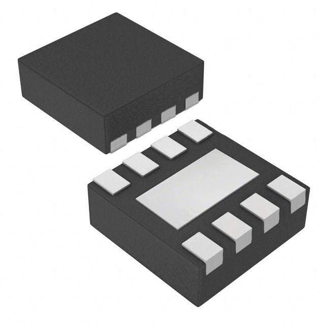
| 产品图片 |
|
| rohs | 符合RoHS无铅 / 符合限制有害物质指令(RoHS)规范要求 |
| 产品系列 | 电源管理 IC,稳压器—开关式稳压器,Texas Instruments TPS62081DSGTDCS-Control™ |
| 数据手册 | |
| 产品型号 | TPS62081DSGT |
| PCN组件/产地 | |
| PWM类型 | 混合物 |
| 产品种类 | 稳压器—开关式稳压器 |
| 供应商器件封装 | 8-WSON (2x2) |
| 其它名称 | 296-29646-2 |
| 包装 | 带卷 (TR) |
| 同步整流器 | 是 |
| 商标 | Texas Instruments |
| 安装类型 | 表面贴装 |
| 安装风格 | SMD/SMT |
| 封装 | Reel |
| 封装/外壳 | 8-WFDFN 裸露焊盘 |
| 封装/箱体 | WSON-8 |
| 工作温度 | -40°C ~ 85°C |
| 工作温度范围 | - 40 C to + 85 C |
| 工厂包装数量 | 250 |
| 开关频率 | 2 MHz |
| 拓扑结构 | Buck |
| 最大工作温度 | + 85 C |
| 最大输入电压 | 6 V |
| 最小工作温度 | - 40 C |
| 最小输入电压 | 2.3 V |
| 标准包装 | 250 |
| 电压-输入 | 2.3 V ~ 6 V |
| 电压-输出 | 1.8V |
| 电流-输出 | 1.2A |
| 类型 | 降压(降压) |
| 系列 | TPS62081 |
| 设计资源 | http://www.digikey.com/product-highlights/cn/zh/texas-instruments-webench-design-center/3176 |
| 输入电压 | 2.3 V to 6 V |
| 输出数 | 1 |
| 输出电压 | 1.8 V |
| 输出电流 | 1.2 A |
| 输出端数量 | 1 Output |
| 输出类型 | 固定 |
| 频率-开关 | 2MHz |


- 商务部:美国ITC正式对集成电路等产品启动337调查
- 曝三星4nm工艺存在良率问题 高通将骁龙8 Gen1或转产台积电
- 太阳诱电将投资9.5亿元在常州建新厂生产MLCC 预计2023年完工
- 英特尔发布欧洲新工厂建设计划 深化IDM 2.0 战略
- 台积电先进制程称霸业界 有大客户加持明年业绩稳了
- 达到5530亿美元!SIA预计今年全球半导体销售额将创下新高
- 英特尔拟将自动驾驶子公司Mobileye上市 估值或超500亿美元
- 三星加码芯片和SET,合并消费电子和移动部门,撤换高东真等 CEO
- 三星电子宣布重大人事变动 还合并消费电子和移动部门
- 海关总署:前11个月进口集成电路产品价值2.52万亿元 增长14.8%


PDF Datasheet 数据手册内容提取
Product Sample & Technical Tools & Support & Folder Buy Documents Software Community TPS62080,TPS62080A,TPS62081,TPS62082 SLVSAE8F–SEPTEMBER2011–REVISEDNOVEMBER2016 TPS6208x 1.2-A High-Efficiency, Step-Down Converter With DCS-Control™ and Snooze Mode 1 Features 3 Description • DCS-Control™ArchitectureforFastTransient The TPS6208x devices are a family of high frequency 1 synchronous step down converters. With an input Regulation voltage range of 2.3 V to 6 V, common battery • SnoozeModefor6.5-µAUltraLowQuiescent technologies are supported. Alternatively, the device Current canbeusedforlowvoltagesystempowerrails. • 2.3-Vto6-VInputVoltageRange The TPS6208x focuses on high efficiency step-down • 100%DutyCycleforLowestDropout conversion over a wide output current range. At • PowerSaveModeforLight-LoadEfficiency medium to heavy loads, the converter operates in PWM mode and automatically enters Power Save • OutputDischargeFunction Mode operation at light load currents to maintain high • Short-CircuitProtection efficiency over the entire load current range. To • Power-GoodOutput maintain high efficiency at very low load or no load • ThermalShutdown currents, a Snooze Mode with an ultra-low quiescent current is implemented. This function, enabled by the • Availablein2-mm ×2-mm8-PinWSONPackage MODE pin, increases the run-time of battery driven applications and keeps the standby current at its 2 Applications lowestleveltomeetgreenenergystandardstargeting • Battery-PoweredPortableDevices alowstand-bycurrent. • PointofLoadRegulators To address the requirements of system power rails, • SystemPowerRailVoltageConversion the internal loop compensation allows a large selection of external output capacitor values in excess of 100 µF. With its DCS-Control™ architecture,excellentloadtransientperformanceand output voltage regulation accuracy is achieved. The device is available in 2-mm × 2-mm WSON package withThermalPAD. DeviceInformation(1) PARTNUMBER PACKAGE BODYSIZE(NOM) TPS62080 TPS62080A WSON(8) 2.00mm×2.00mm TPS62081 TPS62082 (1) For all available packages, see the orderable addendum at theendofthedatasheet. TypicalApplicationSchematic space TPS62081 POWER GOOD 2.3 V .. 6 V V VIN PG 180 k IN 1µH 1.8 V EN SW V 10 µF OUT MODE VOS 22 µF GND FB Copyright © 2016,Texas Instruments Incorporated 1 An IMPORTANT NOTICE at the end of this data sheet addresses availability, warranty, changes, use in safety-critical applications, intellectualpropertymattersandotherimportantdisclaimers.PRODUCTIONDATA.
TPS62080,TPS62080A,TPS62081,TPS62082 SLVSAE8F–SEPTEMBER2011–REVISEDNOVEMBER2016 www.ti.com Table of Contents 1 Features.................................................................. 1 9 ApplicationandImplementation........................ 12 2 Applications........................................................... 1 9.1 ApplicationInformation............................................12 3 Description............................................................. 1 9.2 TypicalApplication..................................................12 4 RevisionHistory..................................................... 2 10 PowerSupplyRecommendations..................... 19 5 DeviceComparisonTable..................................... 4 11 Layout................................................................... 19 6 PinConfigurationandFunctions......................... 4 11.1 LayoutGuidelines.................................................19 11.2 LayoutExample....................................................19 7 Specifications......................................................... 5 11.3 ThermalConsiderations........................................19 7.1 AbsoluteMaximumRatings......................................5 12 DeviceandDocumentationSupport................. 20 7.2 ESDRatings..............................................................5 7.3 RecommendedOperatingConditions.......................5 12.1 DeviceSupport......................................................20 7.4 ThermalInformation..................................................5 12.2 DocumentationSupport........................................20 7.5 ElectricalCharacteristics...........................................6 12.3 RelatedLinks........................................................20 7.6 TypicalCharacteristics..............................................7 12.4 ReceivingNotificationofDocumentationUpdates20 12.5 CommunityResources..........................................20 8 DetailedDescription.............................................. 8 12.6 Trademarks...........................................................20 8.1 Overview...................................................................8 12.7 ElectrostaticDischargeCaution............................20 8.2 FunctionalBlockDiagrams.......................................8 12.8 Glossary................................................................21 8.3 FeatureDescription...................................................9 13 Mechanical,Packaging,andOrderable 8.4 DeviceFunctionalModes........................................11 Information........................................................... 21 4 Revision History NOTE:Pagenumbersforpreviousrevisionsmaydifferfrompagenumbersinthecurrentversion. ChangesfromRevisionE(April2015)toRevisionF Page • ChangedFrom:T =–40°Cto85°CTo:T =–40°Cto125°CintheElectricalCharacteristicsconditionstatement...........6 A J • AddedaTestConditiontoI intheElectricalCharacteristics ............................................................................................. 6 SD • ChangedtheR High-sideTYPvalueFrom:120mΩTo:95mΩintheElectricalCharacteristics................................. 6 DS(on) • ChangedtheR Low-sideTYPvalueFrom:90mΩTo:70mΩintheElectricalCharacteristics.................................... 6 DS(on) • Changedthegraphstoincludea125°CcurveintheTypicalCharacteristics ...................................................................... 7 • Added50ΩvaluetothePowerGoodblockinFigure5........................................................................................................ 8 • Added50ΩvaluetothePowerGoodblockinFigure6........................................................................................................ 9 • AddedTable1 ....................................................................................................................................................................... 9 ChangesfromRevisionD(July2013)toRevisionE Page • AddedPinConfigurationandFunctionssection,ESDRatingstable,FeatureDescriptionsection,DeviceFunctional Modes,ApplicationandImplementationsection,PowerSupplyRecommendationssection,Layoutsection,Device andDocumentationSupportsection,andMechanical,Packaging,andOrderableInformationsection .............................. 1 ChangesfromRevisionC(May2013)toRevisionD Page • DeletedTPS62080ADGNfromORDERINGINFORMATIONtable....................................................................................... 4 • DeletedTPS62080AcolumnfromtheThermalInformationtable.......................................................................................... 5 ChangesfromRevisionB(March2012)toRevisionC Page • ChangedtheThermalInformationtablesvalues.................................................................................................................... 5 2 SubmitDocumentationFeedback Copyright©2011–2016,TexasInstrumentsIncorporated ProductFolderLinks:TPS62080 TPS62080A TPS62081 TPS62082
TPS62080,TPS62080A,TPS62081,TPS62082 www.ti.com SLVSAE8F–SEPTEMBER2011–REVISEDNOVEMBER2016 ChangesfromRevisionA(February2012)toRevisionB Page • ChangedTPS62080ADSGfromProductPreviewtoProductionDatainORDERINGINFORMATION................................ 4 ChangesfromOriginal(September2011)toRevisionA Page • AddedTPS62080Adevice..................................................................................................................................................... 1 • AddedTPS62080ADSG(ProductPreview)andTPS62080ADGN(ProductPreview)toORDERINGINFORMATION....... 4 • AddedTPS62080Aoutputdischargeresistor........................................................................................................................ 6 Copyright©2011–2016,TexasInstrumentsIncorporated SubmitDocumentationFeedback 3 ProductFolderLinks:TPS62080 TPS62080A TPS62081 TPS62082
TPS62080,TPS62080A,TPS62081,TPS62082 SLVSAE8F–SEPTEMBER2011–REVISEDNOVEMBER2016 www.ti.com 5 Device Comparison Table PARTNUMBER(1) OUTPUTVOLTAGE(2) OUTPUTDISCHARGE PACKAGEMARKING PACKAGE RESISTOR TPS62080DSG Adjustable 1kΩ QVR 8-PinWSON TPS62081DSG 1.8V 1kΩ QVS 8-PinWSON TPS62082DSG 3.3V 1kΩ QVT 8-PinWSON TPS62080ADSG Adjustable 40Ω SBN 8-PinWSON (1) Fordetailedorderinginformation,seeMechanical,Packaging,andOrderableInformation. (2) Contactthefactorytocheckavailabilityofotherfixedoutputvoltageversions. 6 Pin Configuration and Functions space DSGPackage 8-PinWSONWithThermalPad (TopView) EN 1 8 VIN D D A GND 2 E P 7 SW S L O A P M MODE 3 X R 6 PG E E H FB 4 T 5 VOS space space PinFunctions PIN I/O DESCRIPTION NAME NO. EN 1 IN DeviceEnableLogicInput. LogicHIGHenablesthedevice,logicLOWdisablesthedeviceandturnsitintoshutdown.Donotleave floating. GND 2 PWR PowerandSignalGround. MODE 3 IN SnoozeModeEnableLogicInput. LogicHIGHenablestheSnoozeMode,logicLOWdisablestheSnoozeMode.Donotleavefloating. FB 4 IN FeedbackPinfortheinternalcontrolloop. Connectthispintotheexternalfeedbackdividerfortheadjustableoutputversions.Forthefixedoutputvoltage versions,thispinmustbeleftfloatingorconnectedtoGND. VOS 5 IN OutputVoltageSensePinfortheinternalcontrolloop.Mustbeconnectedtooutputvoltage. PG 6 OUT PowerGoodopendrainoutput. Thispinispulledtolowiftheoutputvoltageisbelowregulationlimits.Canbeleftfloatingifnotused. SW 7 PWR SwitchPinconnectedtotheinternalMOSFETswitchesandinductorterminal. Connecttheinductoroftheoutputfilterhere. VIN 8 PWR PowerSupplyVoltageInput. Exposed — — ConnectittoGND.Thethermalpadmustbesolderedtoachieveappropriatepowerdissipationand Thermal mechanicalreliability. Pad 4 SubmitDocumentationFeedback Copyright©2011–2016,TexasInstrumentsIncorporated ProductFolderLinks:TPS62080 TPS62080A TPS62081 TPS62082
TPS62080,TPS62080A,TPS62081,TPS62082 www.ti.com SLVSAE8F–SEPTEMBER2011–REVISEDNOVEMBER2016 7 Specifications 7.1 Absolute Maximum Ratings overoperatingfree-airtemperaturerange(unlessotherwisenoted)(1) MIN MAX UNIT VoltageatVIN,PG,VOS(2) –0.3 7 V VoltageatSW(2)(3) –1 7 V VoltageatFB(2) –0.3 3.6 V VoltageatEN,MODE(2) –0.3 VIN+0.3 V SinkcurrentatPG 0 0.5 mA Operatingjunctiontemperature,T –40 150 °C J Storagetemperature,T –65 150 °C stg (1) StressesbeyondthoselistedunderAbsoluteMaximumRatingsmaycausepermanentdamagetothedevice.Thesearestressratings onlyandfunctionaloperationofthedeviceattheseoranyotherconditionsbeyondthoseindicatedunderRecommendedOperating Conditionsisnotimplied.Exposuretoabsolute–maximum–ratedconditionsforextendedperiodsmayaffectdevicereliability. (2) Allvoltagevaluesarewithrespecttonetworkgroundterminal. (3) Duringoperation,deviceswitching. 7.2 ESD Ratings VALUE UNIT Humanbodymodel(HBM),perANSI/ESDA/JEDECJS-001(1) ±2000 V(ESD) Electrostaticdischarge Charged-devicemodel(CDM),perJEDECspecificationJESD22- ±500 V C101(2) (1) JEDECdocumentJEP155statesthat500-VHBMallowssafemanufacturingwithastandardESDcontrolprocess. (2) JEDECdocumentJEP157statesthat250-VCDMallowssafemanufacturingwithastandardESDcontrolprocess. 7.3 Recommended Operating Conditions(1) MIN NOM MAX UNIT V Inputvoltage 2.3 6 V IN V Outputvoltage 0.5 4 V OUT I LoadcurrentinSnoozeMode 2 mA SNOOZE T Operatingjunctiontemperature –40 125 °C J (1) RefertotheApplicationandImplementationsectionforfurtherinformation. 7.4 Thermal Information TPS6208x THERMALMETRIC(1) DSG(WSON) UNIT 8PINS R Junction-to-ambientthermalresistance 59.7 θJA R Junction-to-case(top)thermalresistance 70.1 θJC(top) R Junction-to-boardthermalresistance 30.9 θJB °C/W ψ Junction-to-topcharacterizationparameter 1.4 JT ψ Junction-to-boardcharacterizationparameter 31.5 JB R Junction-to-case(bottom)thermalresistance 8.6 θJC(bot) (1) Formoreinformationabouttraditionalandnewthermalmetrics,seetheSemiconductorandICPackageThermalMetricsapplication report. Copyright©2011–2016,TexasInstrumentsIncorporated SubmitDocumentationFeedback 5 ProductFolderLinks:TPS62080 TPS62080A TPS62081 TPS62082
TPS62080,TPS62080A,TPS62081,TPS62082 SLVSAE8F–SEPTEMBER2011–REVISEDNOVEMBER2016 www.ti.com 7.5 Electrical Characteristics Overrecommendedfree-airtemperaturerange,T =–40°Cto125°C.TypicalvaluesareatT =25°C(unlessotherwise J A noted),V =3.6V,MODE=LOW. IN PARAMETER TESTCONDITIONS MIN TYP MAX UNIT SUPPLY V Inputvoltagerange 2.3 6 V IN QuiescentcurrentintoVIN I =0mA,Devicenotswitching 30 uA OUT IQ QuiescentcurrentintoVIN IOUT=0mA,Devicenotswitching,MODE=HIGH 6.5 uA (SNOOZEMODE) 7 I ShutdowncurrentintoVIN EN=LOW µA SD T =-40°Cto85°C 1 A Undervoltagelockout Inputvoltagefalling 1.8 2 V V UVLO Undervoltagelockouthysteresis RisingaboveV 120 mV UVLO T Thermalshutdown Temperaturerising 150 °C JSD Thermalshutdownhysteresis TemperaturefallingbelowT 20 °C JSD LOGICINTERFACE(ENMODE) V Highlevelinputvoltage 2.3V≤V ≤6V 1 V IH IN V Lowlevelinputvoltage 2.3V≤V ≤6V 0.4 V IL IN I Inputleakagecurrent 0.01 0.5 µA LKG POWERGOOD V Powergoodthreshold V fallingreferencedtoV nominal –15% –10% –5% PG OUT OUT Powergoodhysteresis 5% V Lowlevelvoltage I =500µA 0.3 V OL sink I PGLeakagecurrent V =5.0V 0.01 0.1 µA PG,LKG PG OUTPUT Outputvoltagerange 0.5 4.0 V TPS62080,TPS62080A Outputvoltageaccuracy I =0mA;V ≥2.3V –2.5% 2.5% TPS62081 OUT IN V OUT Outputvoltageaccuracy I =0mA;V ≥3.6V –2.5% 2.5% TPS62082 OUT IN SnoozeModeoutputvoltage MODE=HIGH;V ≥2.3VandV ≥V +1V –5% 5% accuracy IN IN OUT Feedbackregulationvoltage V V ≥2.3VandV ≥V +1V 0.438 0.45 0.462 V FB TPS62080,TPS62080A IN IN OUT Feedbackinputbiascurrent I V =0.45V 10 100 nA FB TPS62080,TPS62080A FB EN=LOW,V =1.8V 1 kΩ OUT R Outputdischargeresistor DIS TPS62080A,EN=LOW,V =1.2V 25 40 65 Ω OUT LineRegulation 0 %/V LoadRegulation TPS62081,TPS62082 –0.25 %/A High-sideFETON-resistance I =500mA 95 mΩ SW R DS(on) Low-sideFETON-resistance I =500mA 70 mΩ SW High-sideFETswitchcurrent I Risinginductorcurrent 1.6 2.8 4 A LIM limit 6 SubmitDocumentationFeedback Copyright©2011–2016,TexasInstrumentsIncorporated ProductFolderLinks:TPS62080 TPS62080A TPS62081 TPS62082
TPS62080,TPS62080A,TPS62081,TPS62082 www.ti.com SLVSAE8F–SEPTEMBER2011–REVISEDNOVEMBER2016 7.6 Typical Characteristics 50 15 45 125°C 125°C 40 12 A) A) µ 35 µ nt ( nt ( e 30 e 9 urr urr C 25 C nt nt e 20 e 6 c c s s uie 15 −40°C 25°C 85°C uie Q Q 10 3 5 −40°C 25°C 85°C 0 0 2.3 2.8 3.3 3.8 4.3 4.8 5.3 5.8 2.3 2.8 3.3 3.8 4.3 4.8 5.3 5.8 Input Voltage (V) Input Voltage (V) G000 G000 Figure1.QuiescentCurrentvsInputVoltageinNormal Figure2.QuiescentCurrentvsInputVoltageinSnooze Mode Mode 350 250 300 200 We (m) 250 125°C e (dB) 125°C Sid 200 85°C Sid 150 85°C − − h w RDSon Hig 110500 25°C RDSon Lo 15000 25°C 50 −40°C −40°C 0 0 2.3 2.8 3.3 3.8 4.3 4.8 5.3 5.8 2.3 2.8 3.3 3.8 4.3 4.8 5.3 5.8 Input Voltage (V) Input Voltage (V) G000 G000 Figure3.High-SideFETR vsInputVoltage Figure4.Low-SideFETR vsInputVoltage DS(on) DS(on) Copyright©2011–2016,TexasInstrumentsIncorporated SubmitDocumentationFeedback 7 ProductFolderLinks:TPS62080 TPS62080A TPS62081 TPS62082
TPS62080,TPS62080A,TPS62081,TPS62082 SLVSAE8F–SEPTEMBER2011–REVISEDNOVEMBER2016 www.ti.com 8 Detailed Description 8.1 Overview The TPS6208x synchronous switched mode converters are based on DCS-Control™ (Direct Control with Seamless transition into Power Save Mode). This is an advanced regulation topology that combines the advantagesofhysteretic,voltageandcurrentmodecontrol. The DCS-Control topology operates in pulse width modulation (PWM) mode for medium to heavy load conditions and in Power Save Mode at light load currents. In PWM mode, the converter operates with its nominal switching frequency of 2 MHz having a controlled frequency variation over the input voltage range. As the load current decreases, the converter enters Power Save Mode, reducing the switching frequency and minimizing the IC quiescent current to achieve high efficiency over the entire load current range. DCS-Control supports both operationmodes(PWMandPFM)usingasinglebuildingblockhavingaseamlesstransitionfromPWMtoPower Save Mode without effects on the output voltage. Fixed output voltage versions provide smallest solution size combined with lowest no load current consumption. The TPS6208x offers both excellent DC voltage and superior loadtransientregulation,combinedwithverylowoutputvoltageripple,minimizinginterferencewithRFcircuits. The device is equipped with Snooze Mode functionality, which is enabled with the MODE pin. Snooze Mode supports high efficiency conversion at lowest output currents below 2 mA. If no load current is drawn, the ultra low quiescent current of 6.5 µA is sufficient to maintain the output voltage. This extends battery run time by reducing the quiescent current during lowest or no load conditions in battery-driven applications. For mains- operated voltage supplies, Snooze Mode reduces the system's stand-by energy consumption. During shutdown (EN=LOW),thedevicereducesenergyconsumptiontolessthan1 µA. 8.2 Functional Block Diagrams MODE VIN High Side Power N-MOS Good PG 50 Gate Control Driver Logic SW Low Side N-MOS Active Output Discharge Thermal Snooze Mode Shutdown GND EN Softstart ramp direct control comparator VOS & compensation Under Voltage FB Lockout error minimum amplifier on-timer REF DCS-CONTROLTM Copyright © 2016,Texas Instruments Incorporated Figure5. FunctionalBlockDiagram(AdjustableOutputVoltageVersion) 8 SubmitDocumentationFeedback Copyright©2011–2016,TexasInstrumentsIncorporated ProductFolderLinks:TPS62080 TPS62080A TPS62081 TPS62082
TPS62080,TPS62080A,TPS62081,TPS62082 www.ti.com SLVSAE8F–SEPTEMBER2011–REVISEDNOVEMBER2016 Functional Block Diagrams (continued) MODE VIN High Side Power N-MOS Good PG 50 Gate Control Driver Logic SW Low Side N-MOS Active Output Discharge Thermal Snooze Mode Shutdown GND EN Softstart ramp direct control comparator VOS & compensation Under Voltage Lockout error minimum amplifier FB on-timer REF DCS-CONTROLTM Copyright © 2016,Texas Instruments Incorporated Figure6. FunctionalBlockDiagram(FixedOutputVoltageVersion) 8.3 Feature Description 8.3.1 PowerGood TheTPS6208xhasapowergoodoutputwhichgoeslowwhentheoutputvoltageisbelowitsnominalvalue.The power good is high impedance once the output is above 95% of the regulated voltage, and is driven to low once the output voltage falls below typically 90% of the regulated voltage. The PG pin is an open drain output and can sink up to 0.5 mA. The power good output requires a pull-up resistor. When the device is off due to disable, UVLO or thermal shutdown, the PG pin is high impedance (see Table 1). The PG signal can be used for sequencing of multiple rails by connecting to the EN pin of other converters. Leave the PG pin unconnected whennotused. space Table1.PowerGoodPinLogicTable PGLogicStatus DeviceInformation HighZ Low V ≥V √ FB PG Enable(EN=High) V ≤V √ FB PG Shutdown(EN=Low) √ UVLO 0.7V<V <V √ IN UVLO ThermalShutdown T >T √ J JSD PowerSupplyRemoval V <0.7V √ IN Copyright©2011–2016,TexasInstrumentsIncorporated SubmitDocumentationFeedback 9 ProductFolderLinks:TPS62080 TPS62080A TPS62081 TPS62082
TPS62080,TPS62080A,TPS62081,TPS62082 SLVSAE8F–SEPTEMBER2011–REVISEDNOVEMBER2016 www.ti.com space 8.3.2 100%DutyCycleLowDropoutOperation The device offers low input to output voltage difference by entering 100% duty cycle mode. In this mode, the high-side MOSFET switch is constantly turned on and the low-side MOSFET is switched off. This is particularly useful in battery powered applications to achieve longest operation time by taking full advantage of the whole batteryvoltagerange.Theminimuminputvoltagetomaintainanoutputvoltageiscalculatedas: V = V +I ´(R +R ) IN,MIN OUT OUT,MAX DS(on) L where • V =Minimuminputvoltage IN,MIN • I =Maximumoutputcurrent OUT,MAX • R =High-sideFETON-resistance DS(on) • R =Inductorohmicresistance (1) L 8.3.3 OutputDischarge The output gets discharged by the SW pin with a typical discharge resistor of R whenever the device shuts DIS down.Thisisthecasewhenthedevicegetsdisabledbyenable,thermalshutdown,orundervoltagelockout.The TPS6208AdiffersfromtheTPS62080onlyinitsstrongerdischarge. 8.3.4 Soft-Start WhenENissettostartdeviceoperation,thedevicestartsswitchingafteradelayofabout40 μsandVOUTrises with a slope of about 10mV/μs (See Figure 27 andFigure 29 for typical startup operation). This avoids excessive inrush current and creates a smooth output voltage rise slope. It also prevents excessive voltage drops of primarycellsandrechargeablebatterieswithhighinternalimpedance. If the output voltage is not reached within the soft start time, such as in the case of heavy load, the converter enters regular operation. Consequently, the inductor current limit operates as described below. The TPS6208x is able to start into a pre-biased output capacitor. The converter starts with the applied bias voltage and ramps up theoutputvoltagetoitsnominalvalue. 8.3.5 UndervoltageLockout To avoid mis-operation of the device at low input voltages, an undervoltage lockout is implemented that shuts downthedeviceatvoltageslowerthanV witha120mVtypicalhysteresis. UVLO 8.3.6 ThermalShutdown The device goes into thermal shutdown once the junction temperature exceeds typically T . Once the device JSD temperaturefallsbelowthethresholdminushysteresis,thedevicereturnstonormaloperationautomatically. 8.3.7 InductorCurrentLimit TheInductorCurrentLimitpreventsthedevicefromhighinductorcurrentanddrawingexcessivecurrentfromthe battery or input voltage rail. Excessive current might occur with a shorted/saturated inductor or a heavy load/shortedoutputcircuitcondition. The incorporated inductor peak current limit measures the current in the high-side and low-side power MOSFET. Once the high-side switch current limit is tripped, the high-side MOSFET is turned off and the low-side MOSFET is turned on to reduce the inductor current. When the inductor current drops down to the low-side switch current limit, the low-side MOSFET is turned off and the high-side switch is turned on again. This operation repeats until the inductor current does not reach the high-side switch current limit. Due to internal propagation delays, the real currentlimitvaluecanexceedthestaticcurrentlimitinElectricalCharacteristics. 10 SubmitDocumentationFeedback Copyright©2011–2016,TexasInstrumentsIncorporated ProductFolderLinks:TPS62080 TPS62080A TPS62081 TPS62082
TPS62080,TPS62080A,TPS62081,TPS62082 www.ti.com SLVSAE8F–SEPTEMBER2011–REVISEDNOVEMBER2016 8.4 Device Functional Modes 8.4.1 EnablingandDisablingtheDevice The device is enabled by setting the EN input to a logic HIGH. Accordingly, a logic LOW disables the device. If the device is enabled, the internal power stage starts switching and regulates the output voltage to the programmedthreshold.TheENinputmustbeterminatedandnotleftfloating. 8.4.2 PowerSaveMode Astheloadcurrentdecreases,theTPS6208xentersPowerSaveModeoperation.DuringPowerSaveMode,the converter operates with reduced switching frequency in PFM mode and with a minimum quiescent current maintaining high efficiency. Power Save Mode occurs when the inductor current becomes discontinuous. It is based on a fixed on time architecture. The typical on time is given by t = 500 ns × (V /V ). The switching on OUT IN frequencyoverthewholeloadcurrentrangeisshowninFigure21andFigure22. 8.4.3 SnoozeMode The TPS6208x offers a Snooze Mode function. If Snooze Mode is enabled by an external logic signal setting the MODE pin to HIGH, the device's quiescent current consumption is reduced to typically 6.5 µA. As a result, the high efficiency range is extended towards the range of lowest output currents below 2 mA. See the efficiency figuresinApplicationCurves. If the device is operating in Snooze Mode, a dedicated, low power consuming block monitors the output voltage. All other control blocks are snoozing during that time. If the output voltage falls below the programmed output voltage by 3.5% (typ), the control blocks wake up, regulate the output voltage and allow themselves to snooze again until the output voltage drops again. Snooze Mode operation provides a clear efficiency improvement at lowest output currents. If the load current increases, the advantage of efficiency in Snooze mode is reduced. Because the dynamic load regulation operates best if Snooze Mode is disabled, it is recommended to turn off SnoozeModewhentheloadcurrentexceeds2mA.Generally,amicrocontrolleroperatestheMODEpin. Copyright©2011–2016,TexasInstrumentsIncorporated SubmitDocumentationFeedback 11 ProductFolderLinks:TPS62080 TPS62080A TPS62081 TPS62082
TPS62080,TPS62080A,TPS62081,TPS62082 SLVSAE8F–SEPTEMBER2011–REVISEDNOVEMBER2016 www.ti.com 9 Application and Implementation NOTE Information in the following applications sections is not part of the TI component specification, and TI does not warrant its accuracy or completeness. TI’s customers are responsible for determining suitability of components for their purposes. Customers should validateandtesttheirdesignimplementationtoconfirmsystemfunctionality. 9.1 Application Information The TPS62080 and TPS62080A are synchronous step-down converter whose output voltage is adjusted by component selection. The following section discusses the design of the external components to complete the power supply design for several input and output voltage options by using typical applications as a reference. TheTPS62081andTPS62082provideafixedoutputvolagewhichdonotneedanexternalresistordivider. 9.2 Typical Application TPS62080 POWER GOOD 2.3 V .. 6 V V VIN PG 178 k IN 1µH EN SW V 10 µF OUT MODE VOS 22 µF R 1 GND FB R 2 Copyright © 2016,Texas Instruments Incorporated Figure7. TypicalApplicationSchematic 9.2.1 DesignRequirements Forthisdesignexample,useTable2astheinputparameters. Table2.DesignParameters DESIGNPARAMETER EXAMPLEVALUE Inputvoltage 2.3Vto6V Outputvoltage 1.2V Outputripplevoltage <20mV Maximumoutputcurrent 1.2A 9.2.2 DetailedDesignProcedure Table3liststhecomponentsusedfortheexample. Table3.ListofComponents REFERENCE DESCRIPTION MANUFACTURER C1 10uF,CeramicCapacitor,6.3V,X5R,size0603 Std 22uF,CeramicCapacitor,6.3V,X5R,size0805, C2 Murata GRM21BR60J226ME39L 1.0µH,PowerInductor,2.2A,size3×3×1.2mm,XFL3012- L1 Coilcraft 102MEB DependingontheoutputvoltageofTPS62080,1%;Notpopulated R1 Std forTPS62081,TPS62082; R2 39.2k,ChipResistor,1/16W,1%,size0603 Std R3 178k,ChipResistor,1/16W,1%,size0603 Std 12 SubmitDocumentationFeedback Copyright©2011–2016,TexasInstrumentsIncorporated ProductFolderLinks:TPS62080 TPS62080A TPS62081 TPS62082
TPS62080,TPS62080A,TPS62081,TPS62082 www.ti.com SLVSAE8F–SEPTEMBER2011–REVISEDNOVEMBER2016 9.2.2.1 SettingtheOutputVoltage The TPS608x devices are available as fixed and adjustable output voltage versions. The fixed voltage versions are internally programmed to a fixed output voltage, whereas the adjustable output voltage version needs to be programmedviaanexternalvoltagedividertosetthedesiredoutputvoltage. 9.2.2.1.1 AdjustableOutputVoltageVersion For the adjustable output voltage version, an external resistor divider is used. By selecting R and R , the output 1 2 voltageisprogrammedtothedesiredvalue. When the output voltage is regulated, the typical voltage at the FB pin is V for the adjustable devices. The FB followingequationcanbeusedtocalculateR andR . 1 2 æ R1ö æ R1ö V =V ´ç1+ ÷=0.45V´ç1+ ÷ OUT FB è R2ø è R2ø (2) For best accuracy, R2 should be kept smaller than 40kΩ to ensure that the current flowing through R2 is at least 100 times larger than I . Changing towards a lower value increases the robustness against noise injection. FB Changing towards higher values reduces the input current. For lowest input current during Snooze Mode, it is recommendedtouseafixedoutputvoltageversionsuchasTPS62081andTPS62082. 9.2.2.2 OutputFilterDesign The inductor and the output capacitor together provide a low pass filter. To simplify this process, Table 4 outlines possible inductor and capacitor value combinations for most applications. Checked cells represent combinations that are proven for stability by simulation and lab test. Further combinations should be checked for each individualapplication. Table4.MatrixofOutputCapacitorandInductorCombinations C [µF](1) L[µH](1) OUT 10 22 47 100 150 0.47 1 + +(2)(3) + + 2.2 + + + + 4.7 (1) Capacitancetoleranceandbiasvoltagede-ratingisanticipated.Theeffectivecapacitancecanvaryby +20%and–50%.Inductortoleranceandcurrentde-ratingisanticipated.Theeffectiveinductancecan varyby+20%and–30%. (2) Plusmarkindicatesrecommendedfiltercombinations. (3) Filtercombinationintypicalapplication. 9.2.2.3 InductorSelection The main parameters for the inductor selection are the inductor value and then the saturation current of the inductor.Tocalculatethemaximuminductorcurrentunderstaticloadconditions,Equation3 isgiven. DI I =I + L L,MAX OUT,MAX 2 V 1- OUT V DI = V ´ IN L OUT L´f SW where • I =Maximumoutputcurrent OUT,MAX • ΔI =Inductorcurrentripple L • f =Switchingfrequency SW • L=Inductorvalue (3) Copyright©2011–2016,TexasInstrumentsIncorporated SubmitDocumentationFeedback 13 ProductFolderLinks:TPS62080 TPS62080A TPS62081 TPS62082
TPS62080,TPS62080A,TPS62081,TPS62082 SLVSAE8F–SEPTEMBER2011–REVISEDNOVEMBER2016 www.ti.com TI recommends to choose the saturation current for the inductor 20%~30% higher than the I , out of L,MAX Equation 3. A higher inductor value is also useful to lower ripple current, but increases the transient response timeaswell.Thefollowinginductorsarerecommendedforuse. Table5.ListofRecommendedInductors INDUCTANCE CURRENTRATING DIMENSIONS DCRESISTANCE [µH] [mA] LxWxH[mm3] [mΩtyp] TYPE MANUFACTURER 1.0 2500 3x3x1.2 35 XFL3012-102ME Coilcraft 1.0 1650 3x3x1.2 40 LQH3NPN1R0NJ0 Murata 2.2 2500 4x3.7x1.65 49 LQH44PN2R2MP0 Murata 2.2 1600 3x3x1.2 81 XFL3012-222ME Coilcraft 9.2.2.4 CapacitorSelection The input capacitor is the low impedance energy source for the converter which helps to provide stable operation. A low ESR multilayer ceramic capacitor is recommended for best filtering and should be placed between VIN and GND as close as possible to those pins. For most applications 10 μF is sufficient, though a largervaluereducesinputcurrentripple. The architecture of the TPS6208X allows the use of tiny ceramic output capacitors with low equivalent series resistance (ESR). These capacitors provide low output voltage ripple and are recommended. To keep its resistance up to high frequencies and to get narrow capacitance variation with temperature, it's recommended to use X7R or X5R dielectric. The TPS6208x is designed to operate with an output capacitance of 10 µF to 100 µF and beyond, as outlined in Table 4. Load transient testing and measuring the bode plot are good ways to verify stabilitywithlargercapacitorvalues. Table6.ListofRecommendedCapacitors CAPACITANCE DIMENSIONS [µF] TYPE LxWxH[mm3] MANUFACTURER 10 GRM188R60J106M 0603:1.6x0.8x0.8 Murata 22 GRM188R60G226M 0603:1.6x0.8x0.8 Murata 22 GRM21BR60J226M 0805:2.0x1.2x1.25 Murata 14 SubmitDocumentationFeedback Copyright©2011–2016,TexasInstrumentsIncorporated ProductFolderLinks:TPS62080 TPS62080A TPS62081 TPS62082
TPS62080,TPS62080A,TPS62081,TPS62082 www.ti.com SLVSAE8F–SEPTEMBER2011–REVISEDNOVEMBER2016 9.2.3 ApplicationCurves 100 100 TPS62080 TPS62080 90 90 VOUT = 0.9 V VOUT = 1.2 V 80 80 70 70 %) %) y ( 60 y ( 60 nc 50 nc 50 e e Effici 3400 VVIINN == 23..86 VV Effici 3400 VVIINN == 23..86 VV VIN = 4.2 V VIN = 4.2 V 20 VIN = 2.8 V, Snooze Mode 20 VIN = 2.8 V, Snooze Mode 10 VIN = 3.6 V, Snooze Mode 10 VIN = 3.6 V, Snooze Mode VIN = 4.2 V, Snooze Mode VIN = 4.2 V, Snooze Mode 0 0 10u 100u 1m 10m 100m 1 3 10u 100u 1m 10m 100m 1 3 Output Current (A) Output Current (A) G001 G002 Figure8.EfficiencyvsLoadCurrent Figure9.EfficiencyvsLoadCurrent 100 100 TPS62080 TPS62081 90 90 VOUT = 2.5 V VOUT = 1.8 V 80 80 70 70 %) %) y ( 60 y ( 60 nc 50 nc 50 e e Effici 3400 VVIINN == 34..62 VV Effici 3400 VVIINN == 23..86 VV VIN = 5.0 V VIN = 4.2 V 20 VIN = 3.6 V, Snooze Mode 20 VIN = 2.8 V, Snooze Mode 10 VIN = 4.2 V, Snooze Mode 10 VIN = 3.6 V, Snooze Mode VIN = 5.0 V, Snooze Mode VIN = 4.2 V, Snooze Mode 0 0 10u 100u 1m 10m 100m 1 3 10u 100u 1m 10m 100m 1 3 Output Current (A) Output Current (A) G003 G005 Figure10.EfficiencyvsLoadCurrent Figure11.EfficiencyvsLoadCurrent 100 0.910 90 0.905 80 ency (%) 567000 TVPOUST6 =2 038.32 V Voltage (V) 00..899050 Effici 3400 VVVIIINNN === 345...620 VVV Output 0.890 IIIOOOUUUTTT === 111AAA,,, TTTAAA === 2−8554°°0CC°C 20 VIN = 3.6 V, Snooze Mode 0.885 IOUT = 10mA, TA = 25°C 10 VIN = 4.2 V, Snooze Mode TPS62080 IOUT = 10mA, TA = −40°C VIN = 5.0 V, Snooze Mode VOUT = 0.9 V IOUT = 10mA, TA = 85°C 0 0.880 10u 100u 1m 10m 100m 1 3 2.3 2.8 3.3 3.8 4.3 4.8 5.3 5.8 Output Current (A) Input Voltage (V) G004 G006 Figure12.EfficiencyvsLoadCurrent Figure13.OutputVoltagevsInputVoltage Copyright©2011–2016,TexasInstrumentsIncorporated SubmitDocumentationFeedback 15 ProductFolderLinks:TPS62080 TPS62080A TPS62081 TPS62082
TPS62080,TPS62080A,TPS62081,TPS62082 SLVSAE8F–SEPTEMBER2011–REVISEDNOVEMBER2016 www.ti.com 2.56 1.86 TPS62080 TPS62081 2.54 VOUT = 2.5 V 1.84 VOUT = 1.8 V 1.82 e (V) 2.52 e (V) 1.80 g g a a olt 2.50 olt 1.78 V V put IOUT = 1A, TA = 25°C put 1.76 IOUT = 1A, TA = 25°C ut 2.48 IOUT = 1A, TA = −40°C ut IOUT = 1A, TA = −40°C O IOUT = 1A, TA = 85°C O 1.74 IOUT = 1A, TA = 85°C 2.46 IOUT = 10mA, TA = 25°C IOUT = 10mA, TA = 25°C IOUT = 10mA, TA = −40°C 1.72 IOUT = 10mA, TA = −40°C IOUT = 10mA, TA = 85°C IOUT = 10mA, TA = 85°C 2.44 1.70 2.5 3 3.5 4 4.5 5 5.5 6 2.3 2.8 3.3 3.8 4.3 4.8 5.3 5.8 Input Voltage (V) Input Voltage (V) G007 G008 Figure14.OutputVoltagevsInputVoltage Figure15.OutputVoltagevsInputVoltage 3.36 0.910 TPS62082 TPS62080 3.34 VOUT = 3.3 V 0.908 VIN = 3.6 V 3.32 0.906 ge (V) 3.30 ge (V) 00..990024 a 3.28 a olt olt 0.900 put V 3.26 IOUT = 1A, TA = 25°C put V 0.898 Out 3.24 IIOOUUTT == 11AA,, TTAA == −854°0C°C Out 0.896 3.22 IOUT = 10mA, TA = 25°C 0.894 TA = 25°C 3.20 IOUT = 10mA, TA = −40°C 0.892 TA = −40°C IOUT = 10mA, TA = 85°C TA = 85°C 3.18 0.890 3.3 3.8 4.3 4.8 5.3 5.8 10u 100u 1m 10m 100m 1 3 Input Voltage (V) Output Current (A) G009 G010 Figure16.OutputVoltagevsInputVoltage Figure17.OutputVoltagevsLoadCurrent 2.54 1.84 TPS62080 TPS62081 VIN = 3.6 V VIN = 3.6 V 2.52 1.82 V) V) e ( e ( g g a a olt 2.50 olt 1.80 V V ut ut p p ut ut O O 2.48 1.78 TA = 25°C TA = 25°C TA = −40°C TA = −40°C TA = 85°C TA = 85°C 2.46 1.76 10u 100u 1m 10m 100m 1 3 10u 100u 1m 10m 100m 1 3 Output Current (A) Output Current (A) G011 G012 Figure18.OutputVoltagevsLoadCurrent Figure19.OutputVoltagevsLoadCurrent 16 SubmitDocumentationFeedback Copyright©2011–2016,TexasInstrumentsIncorporated ProductFolderLinks:TPS62080 TPS62080A TPS62081 TPS62082
TPS62080,TPS62080A,TPS62081,TPS62082 www.ti.com SLVSAE8F–SEPTEMBER2011–REVISEDNOVEMBER2016 3.34 3M TPS62082 TPS62080 VIN = 3.6 V 2.5M VOUT = 0.9V 3.32 z) H ge (V) 3.30 ency ( 2M a u olt eq 1.5M ut V 3.28 g Fr p n ut hi 1M O witc VIN = 2.3V 3.26 TA = 25°C S 500k VIN = 3.3V TA = −40°C VIN = 4.2V TA = 85°C VIN = 5.0V 3.24 0 10u 100u 1m 10m 100m 1 3 0 400m 800m 1.2 1.6 Output Current (A) Output Current (A) G013 G014 Figure20.OutputVoltagevsLoadCurrent Figure21.SwitchingFrequencyvsLoadCurrent 4.5M TPS62080 VIN = 2.5V 4M VOUT = 2.5V VIN = 3.3V z) 3.5M VIN = 4.2V cy (H 3M VIN = 5.0V SW en (2 V/div) u 2.5M q e Fr 2M g n witchi 1.15MM V(2O0U mTV/div) S 500k 0 ICOIL 0 400m 800m 1.2 1.6 (0.5 A/div) Output Current (A) G015 Time (200 ns/div) V =3.3V,V =1.2V,LoadCurrent=500mA IN OUT Figure22.SwitchingFrequencyvsLoadCurrent Figure23.TypicalApplication(PWMMode) SW SW (2 V/div) 2V/div VOUT VOUT (20 mV/div) 50mV/div ICOIL ICOIL (0.2 A/div) 0.2A/div Time (2µs/div) t - 50µs/div V =3.3V,V =1.2V,LoadCurrent=10mA V =3.3V,V =1.2V,LoadCurrent=2mA IN OUT IN OUT Figure24.TypicalApplication(PFMMode) Figure25.TypicalApplication(SnoozeMode) Copyright©2011–2016,TexasInstrumentsIncorporated SubmitDocumentationFeedback 17 ProductFolderLinks:TPS62080 TPS62080A TPS62081 TPS62082
TPS62080,TPS62080A,TPS62081,TPS62082 SLVSAE8F–SEPTEMBER2011–REVISEDNOVEMBER2016 www.ti.com 1 A 4.2 V LOAD (1 A/div) 50 mA VIN (1 V/div) 3.3 V VOUT (20 mV/div) VOUT (50 mV/div) ICOIL (1 A/div) Time (50µs/div) Time (100µs/div) V =3.3V,V =1.2V,LoadCurrent=50mAto1A V =3.3Vto4.2V,V =1.2V,Load=2.2Ω IN OUT IN OUT Figure26.LoadTransient Figure27.LineTransient EN EN (5 V/div) (5 V/div) PG PG (1 V/div) (1 V/div) VOUT VOUT (1 V/div) (1 V/div) ICOIL ICOIL (0.5 A/div) (0.2 A/div) Time (20µs/div) Time (20µs/div) VIN=3.3V,VOUT=1.2V,Load=2.2Ω VIN=3.3V,VOUT=1.2V,NoLoad Figure28.StartUp Figure29.StartUp(WithoutLoad) EN 5V/div V OUT 0.5V/div t - 20ms/div V =3.3V,V =1.2V,NoLoad IN OUT Figure30.Shutdown 18 SubmitDocumentationFeedback Copyright©2011–2016,TexasInstrumentsIncorporated ProductFolderLinks:TPS62080 TPS62080A TPS62081 TPS62082
TPS62080,TPS62080A,TPS62081,TPS62082 www.ti.com SLVSAE8F–SEPTEMBER2011–REVISEDNOVEMBER2016 10 Power Supply Recommendations The device is designed to operate from an input supply voltage range between 2.3 V and 6 V. Ensure that the inputpowersupplyhasasufficientcurrentratingfortheapplication. 11 Layout 11.1 Layout Guidelines ThePCBlayoutisanimportantsteptomaintainthehighperformanceoftheTPS6208xdevices. The input/output capacitors and the inductor should be placed as close as possible to the IC. This keeps the traces short. Routing these traces direct and wide results in low trace resistance and low parasitic inductance. A common power GND should be used. The low-side of the input and output capacitors must be connected properlytothepowerGNDtoavoidaGNDpotentialshift. The sense traces connected to the FB and VOS pins are signal traces. Special care should be taken to avoid noise being induced. By a direct routing, parasitic inductance can be kept small. GND layers might be used for shielding.KeepthesetracesawayfromSWnodes. 11.2 Layout Example space L1 VOUT VIN C1 VIN SW PG VOS C2 GND EN GND MODE FB GND R1 R2 Figure31. PCBLayoutSuggestion 11.3 Thermal Considerations Implementation of integrated circuits in low-profile and fine-pitch surface-mount packages typically requires special attention to power dissipation. Many system-dependent issues such as thermal coupling, airflow, added heat sinks and convection surfaces, and the presence of other heat-generating components affect the power- dissipationlimitsofagivencomponent. Threebasicapproachesforenhancingthermalperformancearelistedbelow: • ImprovingthepowerdissipationcapabilityofthePCBdesign • ImprovingthethermalcouplingofthecomponenttothePCBbysolderingExposedThermalPad • Introducingairflowinthesystem For more details on how to use the thermal parameters, see the application notes: Thermal Characteristics of LinearandLogicPackagesUsingJEDECPCBDesigns (SZZA017)andSemiconductorandICPackageThermal Metrics(SPRA953). Copyright©2011–2016,TexasInstrumentsIncorporated SubmitDocumentationFeedback 19 ProductFolderLinks:TPS62080 TPS62080A TPS62081 TPS62082
TPS62080,TPS62080A,TPS62081,TPS62082 SLVSAE8F–SEPTEMBER2011–REVISEDNOVEMBER2016 www.ti.com 12 Device and Documentation Support 12.1 Device Support 12.1.1 Third-PartyProductsDisclaimer TI'S PUBLICATION OF INFORMATION REGARDING THIRD-PARTY PRODUCTS OR SERVICES DOES NOT CONSTITUTE AN ENDORSEMENT REGARDING THE SUITABILITY OF SUCH PRODUCTS OR SERVICES OR A WARRANTY, REPRESENTATION OR ENDORSEMENT OF SUCH PRODUCTS OR SERVICES, EITHER ALONEORINCOMBINATIONWITHANYTIPRODUCTORSERVICE. 12.2 Documentation Support 12.2.1 RelatedDocumentation Forrelateddocumentationseethefollowing: ThermalCharacteristicsofLinearandLogicPackagesUsingJEDECPCBDesigns (SZZA017) 12.3 Related Links The table below lists quick access links. Categories include technical documents, support and community resources,toolsandsoftware,andquickaccesstosampleorbuy. Table7.RelatedLinks TECHNICAL TOOLS& SUPPORT& PARTS PRODUCTFOLDER SAMPLE&BUY DOCUMENTS SOFTWARE COMMUNITY TPS62080 Clickhere Clickhere Clickhere Clickhere Clickhere TPS62080A Clickhere Clickhere Clickhere Clickhere Clickhere TPS62081 Clickhere Clickhere Clickhere Clickhere Clickhere TPS62082 Clickhere Clickhere Clickhere Clickhere Clickhere 12.4 Receiving Notification of Documentation Updates To receive notification of documentation updates, navigate to the device product folder on ti.com. In the upper right corner, click on Alert me to register and receive a weekly digest of any product information that has changed.Forchangedetails,reviewtherevisionhistoryincludedinanyreviseddocument. 12.5 Community Resources The following links connect to TI community resources. Linked contents are provided "AS IS" by the respective contributors. They do not constitute TI specifications and do not necessarily reflect TI's views; see TI's Terms of Use. TIE2E™OnlineCommunity TI'sEngineer-to-Engineer(E2E)Community.Createdtofostercollaboration amongengineers.Ate2e.ti.com,youcanaskquestions,shareknowledge,exploreideasandhelp solveproblemswithfellowengineers. DesignSupport TI'sDesignSupport QuicklyfindhelpfulE2Eforumsalongwithdesignsupporttoolsand contactinformationfortechnicalsupport. 12.6 Trademarks DCS-Control,E2EaretrademarksofTexasInstruments. Allothertrademarksarethepropertyoftheirrespectiveowners. 12.7 Electrostatic Discharge Caution Thesedeviceshavelimitedbuilt-inESDprotection.Theleadsshouldbeshortedtogetherorthedeviceplacedinconductivefoam duringstorageorhandlingtopreventelectrostaticdamagetotheMOSgates. 20 SubmitDocumentationFeedback Copyright©2011–2016,TexasInstrumentsIncorporated ProductFolderLinks:TPS62080 TPS62080A TPS62081 TPS62082
TPS62080,TPS62080A,TPS62081,TPS62082 www.ti.com SLVSAE8F–SEPTEMBER2011–REVISEDNOVEMBER2016 12.8 Glossary SLYZ022—TIGlossary. Thisglossarylistsandexplainsterms,acronyms,anddefinitions. 13 Mechanical, Packaging, and Orderable Information The following pages include mechanical, packaging, and orderable information. This information is the most current data available for the designated devices. This data is subject to change without notice and revision of thisdocument.Forbrowser-basedversionsofthisdatasheet,refertotheleft-handnavigation. Copyright©2011–2016,TexasInstrumentsIncorporated SubmitDocumentationFeedback 21 ProductFolderLinks:TPS62080 TPS62080A TPS62081 TPS62082
PACKAGE OPTION ADDENDUM www.ti.com 6-Feb-2020 PACKAGING INFORMATION Orderable Device Status Package Type Package Pins Package Eco Plan Lead/Ball Finish MSL Peak Temp Op Temp (°C) Device Marking Samples (1) Drawing Qty (2) (6) (3) (4/5) TPS62080ADSGR ACTIVE WSON DSG 8 3000 Green (RoHS NIPDAU Level-2-260C-1 YEAR -40 to 125 SBN & no Sb/Br) TPS62080ADSGT ACTIVE WSON DSG 8 250 Green (RoHS NIPDAU Level-2-260C-1 YEAR -40 to 125 SBN & no Sb/Br) TPS62080DSGR ACTIVE WSON DSG 8 3000 Green (RoHS NIPDAU Level-2-260C-1 YEAR -40 to 125 QVR & no Sb/Br) TPS62080DSGT ACTIVE WSON DSG 8 250 Green (RoHS NIPDAU Level-2-260C-1 YEAR -40 to 125 QVR & no Sb/Br) TPS62081DSGR ACTIVE WSON DSG 8 3000 Green (RoHS NIPDAU Level-2-260C-1 YEAR -40 to 125 QVS & no Sb/Br) TPS62081DSGT ACTIVE WSON DSG 8 250 Green (RoHS NIPDAU Level-2-260C-1 YEAR -40 to 125 QVS & no Sb/Br) TPS62082DSGR ACTIVE WSON DSG 8 3000 Green (RoHS NIPDAU Level-2-260C-1 YEAR -40 to 125 QVT & no Sb/Br) TPS62082DSGT ACTIVE WSON DSG 8 250 Green (RoHS NIPDAU Level-2-260C-1 YEAR -40 to 125 QVT & no Sb/Br) (1) The marketing status values are defined as follows: ACTIVE: Product device recommended for new designs. LIFEBUY: TI has announced that the device will be discontinued, and a lifetime-buy period is in effect. NRND: Not recommended for new designs. Device is in production to support existing customers, but TI does not recommend using this part in a new design. PREVIEW: Device has been announced but is not in production. Samples may or may not be available. OBSOLETE: TI has discontinued the production of the device. (2) RoHS: TI defines "RoHS" to mean semiconductor products that are compliant with the current EU RoHS requirements for all 10 RoHS substances, including the requirement that RoHS substance do not exceed 0.1% by weight in homogeneous materials. Where designed to be soldered at high temperatures, "RoHS" products are suitable for use in specified lead-free processes. TI may reference these types of products as "Pb-Free". RoHS Exempt: TI defines "RoHS Exempt" to mean products that contain lead but are compliant with EU RoHS pursuant to a specific EU RoHS exemption. Green: TI defines "Green" to mean the content of Chlorine (Cl) and Bromine (Br) based flame retardants meet JS709B low halogen requirements of <=1000ppm threshold. Antimony trioxide based flame retardants must also meet the <=1000ppm threshold requirement. (3) MSL, Peak Temp. - The Moisture Sensitivity Level rating according to the JEDEC industry standard classifications, and peak solder temperature. (4) There may be additional marking, which relates to the logo, the lot trace code information, or the environmental category on the device. Addendum-Page 1
PACKAGE OPTION ADDENDUM www.ti.com 6-Feb-2020 (5) Multiple Device Markings will be inside parentheses. Only one Device Marking contained in parentheses and separated by a "~" will appear on a device. If a line is indented then it is a continuation of the previous line and the two combined represent the entire Device Marking for that device. (6) Lead/Ball Finish - Orderable Devices may have multiple material finish options. Finish options are separated by a vertical ruled line. Lead/Ball Finish values may wrap to two lines if the finish value exceeds the maximum column width. Important Information and Disclaimer:The information provided on this page represents TI's knowledge and belief as of the date that it is provided. TI bases its knowledge and belief on information provided by third parties, and makes no representation or warranty as to the accuracy of such information. Efforts are underway to better integrate information from third parties. TI has taken and continues to take reasonable steps to provide representative and accurate information but may not have conducted destructive testing or chemical analysis on incoming materials and chemicals. TI and TI suppliers consider certain information to be proprietary, and thus CAS numbers and other limited information may not be available for release. In no event shall TI's liability arising out of such information exceed the total purchase price of the TI part(s) at issue in this document sold by TI to Customer on an annual basis. Addendum-Page 2
PACKAGE MATERIALS INFORMATION www.ti.com 4-Jan-2020 TAPE AND REEL INFORMATION *Alldimensionsarenominal Device Package Package Pins SPQ Reel Reel A0 B0 K0 P1 W Pin1 Type Drawing Diameter Width (mm) (mm) (mm) (mm) (mm) Quadrant (mm) W1(mm) TPS62080ADSGR WSON DSG 8 3000 178.0 8.4 2.25 2.25 1.0 4.0 8.0 Q2 TPS62080ADSGT WSON DSG 8 250 178.0 8.4 2.25 2.25 1.0 4.0 8.0 Q2 TPS62080DSGR WSON DSG 8 3000 178.0 8.4 2.25 2.25 1.0 4.0 8.0 Q2 TPS62080DSGT WSON DSG 8 250 178.0 8.4 2.25 2.25 1.0 4.0 8.0 Q2 TPS62080DSGT WSON DSG 8 250 179.0 8.4 2.2 2.2 1.2 4.0 8.0 Q2 TPS62081DSGR WSON DSG 8 3000 178.0 8.4 2.25 2.25 1.0 4.0 8.0 Q2 TPS62081DSGT WSON DSG 8 250 178.0 8.4 2.25 2.25 1.0 4.0 8.0 Q2 TPS62082DSGR WSON DSG 8 3000 179.0 8.4 2.2 2.2 1.2 4.0 8.0 Q2 TPS62082DSGR WSON DSG 8 3000 178.0 8.4 2.25 2.25 1.0 4.0 8.0 Q2 TPS62082DSGT WSON DSG 8 250 178.0 8.4 2.25 2.25 1.0 4.0 8.0 Q2 TPS62082DSGT WSON DSG 8 250 179.0 8.4 2.2 2.2 1.2 4.0 8.0 Q2 PackMaterials-Page1
PACKAGE MATERIALS INFORMATION www.ti.com 4-Jan-2020 *Alldimensionsarenominal Device PackageType PackageDrawing Pins SPQ Length(mm) Width(mm) Height(mm) TPS62080ADSGR WSON DSG 8 3000 205.0 200.0 33.0 TPS62080ADSGT WSON DSG 8 250 205.0 200.0 33.0 TPS62080DSGR WSON DSG 8 3000 205.0 200.0 33.0 TPS62080DSGT WSON DSG 8 250 205.0 200.0 33.0 TPS62080DSGT WSON DSG 8 250 195.0 200.0 45.0 TPS62081DSGR WSON DSG 8 3000 205.0 200.0 33.0 TPS62081DSGT WSON DSG 8 250 205.0 200.0 33.0 TPS62082DSGR WSON DSG 8 3000 195.0 200.0 45.0 TPS62082DSGR WSON DSG 8 3000 205.0 200.0 33.0 TPS62082DSGT WSON DSG 8 250 205.0 200.0 33.0 TPS62082DSGT WSON DSG 8 250 195.0 200.0 45.0 PackMaterials-Page2
GENERIC PACKAGE VIEW DSG 8 WSON - 0.8 mm max height 2 x 2, 0.5 mm pitch PLASTIC SMALL OUTLINE - NO LEAD This image is a representation of the package family, actual package may vary. Refer to the product data sheet for package details. 4224783/A www.ti.com
PACKAGE OUTLINE DSG0008A WSON - 0.8 mm max height SCALE 5.500 PLASTIC SMALL OUTLINE - NO LEAD 2.1 B A 1.9 PIN 1 INDEX AREA 2.1 1.9 0.32 0.18 0.4 0.2 OPTIONAL TERMINAL TYPICAL 0.8 MAX C SEATING PLANE 0.05 0.08 C 0.00 EXPOSED THERMAL PAD 0.9 0.1 (0.2) TYP 5 4 6X 0.5 2X 9 1.5 1.6 0.1 8 1 SEE OPTIONAL TERMINAL 0.32 8X PIN 1 ID 8X 0.4 0.18 0.2 0.1 C A B 0.05 C 4218900/C 04/2019 NOTES: 1. All linear dimensions are in millimeters. Any dimensions in parenthesis are for reference only. Dimensioning and tolerancing per ASME Y14.5M. 2. This drawing is subject to change without notice. 3. The package thermal pad must be soldered to the printed circuit board for thermal and mechanical performance. www.ti.com
EXAMPLE BOARD LAYOUT DSG0008A WSON - 0.8 mm max height PLASTIC SMALL OUTLINE - NO LEAD (0.9) ( 0.2) VIA 8X (0.5) TYP 1 8 8X (0.25) (0.55) SYMM 9 (1.6) 6X (0.5) 5 4 (R0.05) TYP SYMM (1.9) LAND PATTERN EXAMPLE SCALE:20X 0.07 MAX 0.07 MIN ALL AROUND ALL AROUND SOLDER MASK METAL METAL UNDER SOLDER MASK OPENING SOLDER MASK OPENING NON SOLDER MASK SOLDER MASK DEFINED DEFINED (PREFERRED) SOLDER MASK DETAILS 4218900/C 04/2019 NOTES: (continued) 4. This package is designed to be soldered to a thermal pad on the board. For more information, see Texas Instruments literature number SLUA271 (www.ti.com/lit/slua271). 5. Vias are optional depending on application, refer to device data sheet. If any vias are implemented, refer to their locations shown on this view. It is recommended that vias under paste be filled, plugged or tented. www.ti.com
EXAMPLE STENCIL DESIGN DSG0008A WSON - 0.8 mm max height PLASTIC SMALL OUTLINE - NO LEAD 8X (0.5) SYMM METAL 1 8 8X (0.25) (0.45) SYMM 9 (0.7) 6X (0.5) 5 4 (R0.05) TYP (0.9) (1.9) SOLDER PASTE EXAMPLE BASED ON 0.125 mm THICK STENCIL EXPOSED PAD 9: 87% PRINTED SOLDER COVERAGE BY AREA UNDER PACKAGE SCALE:25X 4218900/C 04/2019 NOTES: (continued) 6. Laser cutting apertures with trapezoidal walls and rounded corners may offer better paste release. IPC-7525 may have alternate design recommendations. www.ti.com
IMPORTANTNOTICEANDDISCLAIMER TI PROVIDES TECHNICAL AND RELIABILITY DATA (INCLUDING DATASHEETS), DESIGN RESOURCES (INCLUDING REFERENCE DESIGNS), APPLICATION OR OTHER DESIGN ADVICE, WEB TOOLS, SAFETY INFORMATION, AND OTHER RESOURCES “AS IS” AND WITH ALL FAULTS, AND DISCLAIMS ALL WARRANTIES, EXPRESS AND IMPLIED, INCLUDING WITHOUT LIMITATION ANY IMPLIED WARRANTIES OF MERCHANTABILITY, FITNESS FOR A PARTICULAR PURPOSE OR NON-INFRINGEMENT OF THIRD PARTY INTELLECTUAL PROPERTY RIGHTS. These resources are intended for skilled developers designing with TI products. You are solely responsible for (1) selecting the appropriate TI products for your application, (2) designing, validating and testing your application, and (3) ensuring your application meets applicable standards, and any other safety, security, or other requirements. These resources are subject to change without notice. TI grants you permission to use these resources only for development of an application that uses the TI products described in the resource. Other reproduction and display of these resources is prohibited. No license is granted to any other TI intellectual property right or to any third party intellectual property right. TI disclaims responsibility for, and you will fully indemnify TI and its representatives against, any claims, damages, costs, losses, and liabilities arising out of your use of these resources. TI’s products are provided subject to TI’s Terms of Sale (www.ti.com/legal/termsofsale.html) or other applicable terms available either on ti.com or provided in conjunction with such TI products. TI’s provision of these resources does not expand or otherwise alter TI’s applicable warranties or warranty disclaimers for TI products. Mailing Address: Texas Instruments, Post Office Box 655303, Dallas, Texas 75265 Copyright © 2020, Texas Instruments Incorporated